US6147362A - High performance display pixel for electronics displays - Google Patents
High performance display pixel for electronics displays Download PDFInfo
- Publication number
- US6147362A US6147362A US08/819,413 US81941397A US6147362A US 6147362 A US6147362 A US 6147362A US 81941397 A US81941397 A US 81941397A US 6147362 A US6147362 A US 6147362A
- Authority
- US
- United States
- Prior art keywords
- region
- display
- voltage
- voltage transistor
- pixel
- Prior art date
- Legal status (The legal status is an assumption and is not a legal conclusion. Google has not performed a legal analysis and makes no representation as to the accuracy of the status listed.)
- Expired - Lifetime
Links
- 239000011159 matrix material Substances 0.000 claims abstract description 13
- 239000012212 insulator Substances 0.000 claims description 12
- 239000010409 thin film Substances 0.000 claims description 4
- 230000003071 parasitic effect Effects 0.000 abstract description 5
- 230000004044 response Effects 0.000 abstract description 5
- 208000032750 Device leakage Diseases 0.000 abstract 1
- XUIMIQQOPSSXEZ-UHFFFAOYSA-N Silicon Chemical compound [Si] XUIMIQQOPSSXEZ-UHFFFAOYSA-N 0.000 description 8
- 229910052710 silicon Inorganic materials 0.000 description 8
- 239000010703 silicon Substances 0.000 description 8
- 238000000034 method Methods 0.000 description 6
- 239000004065 semiconductor Substances 0.000 description 6
- 239000000758 substrate Substances 0.000 description 5
- 230000000903 blocking effect Effects 0.000 description 4
- 230000006872 improvement Effects 0.000 description 4
- 229910052751 metal Inorganic materials 0.000 description 4
- 239000002184 metal Substances 0.000 description 4
- 230000008569 process Effects 0.000 description 4
- VYPSYNLAJGMNEJ-UHFFFAOYSA-N silicon dioxide Inorganic materials O=[Si]=O VYPSYNLAJGMNEJ-UHFFFAOYSA-N 0.000 description 4
- 230000008878 coupling Effects 0.000 description 3
- 238000010168 coupling process Methods 0.000 description 3
- 238000005859 coupling reaction Methods 0.000 description 3
- 239000000463 material Substances 0.000 description 3
- 235000012239 silicon dioxide Nutrition 0.000 description 3
- OAICVXFJPJFONN-UHFFFAOYSA-N Phosphorus Chemical compound [P] OAICVXFJPJFONN-UHFFFAOYSA-N 0.000 description 2
- 230000015572 biosynthetic process Effects 0.000 description 2
- 239000011521 glass Substances 0.000 description 2
- 238000012986 modification Methods 0.000 description 2
- 230000004048 modification Effects 0.000 description 2
- 239000010453 quartz Substances 0.000 description 2
- 230000035945 sensitivity Effects 0.000 description 2
- 230000001808 coupling effect Effects 0.000 description 1
- 238000005516 engineering process Methods 0.000 description 1
- 238000005530 etching Methods 0.000 description 1
- AMGQUBHHOARCQH-UHFFFAOYSA-N indium;oxotin Chemical compound [In].[Sn]=O AMGQUBHHOARCQH-UHFFFAOYSA-N 0.000 description 1
- 238000002347 injection Methods 0.000 description 1
- 239000007924 injection Substances 0.000 description 1
- 238000004519 manufacturing process Methods 0.000 description 1
- 230000000873 masking effect Effects 0.000 description 1
- 238000001465 metallisation Methods 0.000 description 1
- 230000035515 penetration Effects 0.000 description 1
- 230000000750 progressive effect Effects 0.000 description 1
- 229910021332 silicide Inorganic materials 0.000 description 1
- FVBUAEGBCNSCDD-UHFFFAOYSA-N silicide(4-) Chemical compound [Si-4] FVBUAEGBCNSCDD-UHFFFAOYSA-N 0.000 description 1
- 239000000377 silicon dioxide Substances 0.000 description 1
- 238000003860 storage Methods 0.000 description 1
Images
Classifications
-
- H—ELECTRICITY
- H01—ELECTRIC ELEMENTS
- H01L—SEMICONDUCTOR DEVICES NOT COVERED BY CLASS H10
- H01L27/00—Devices consisting of a plurality of semiconductor or other solid-state components formed in or on a common substrate
- H01L27/02—Devices consisting of a plurality of semiconductor or other solid-state components formed in or on a common substrate including semiconductor components specially adapted for rectifying, oscillating, amplifying or switching and having at least one potential-jump barrier or surface barrier; including integrated passive circuit elements with at least one potential-jump barrier or surface barrier
- H01L27/12—Devices consisting of a plurality of semiconductor or other solid-state components formed in or on a common substrate including semiconductor components specially adapted for rectifying, oscillating, amplifying or switching and having at least one potential-jump barrier or surface barrier; including integrated passive circuit elements with at least one potential-jump barrier or surface barrier the substrate being other than a semiconductor body, e.g. an insulating body
- H01L27/1214—Devices consisting of a plurality of semiconductor or other solid-state components formed in or on a common substrate including semiconductor components specially adapted for rectifying, oscillating, amplifying or switching and having at least one potential-jump barrier or surface barrier; including integrated passive circuit elements with at least one potential-jump barrier or surface barrier the substrate being other than a semiconductor body, e.g. an insulating body comprising a plurality of TFTs formed on a non-semiconducting substrate, e.g. driving circuits for AMLCDs
-
- H—ELECTRICITY
- H01—ELECTRIC ELEMENTS
- H01L—SEMICONDUCTOR DEVICES NOT COVERED BY CLASS H10
- H01L29/00—Semiconductor devices adapted for rectifying, amplifying, oscillating or switching, or capacitors or resistors with at least one potential-jump barrier or surface barrier, e.g. PN junction depletion layer or carrier concentration layer; Details of semiconductor bodies or of electrodes thereof ; Multistep manufacturing processes therefor
- H01L29/66—Types of semiconductor device ; Multistep manufacturing processes therefor
- H01L29/68—Types of semiconductor device ; Multistep manufacturing processes therefor controllable by only the electric current supplied, or only the electric potential applied, to an electrode which does not carry the current to be rectified, amplified or switched
- H01L29/76—Unipolar devices, e.g. field effect transistors
- H01L29/772—Field effect transistors
- H01L29/78—Field effect transistors with field effect produced by an insulated gate
- H01L29/786—Thin film transistors, i.e. transistors with a channel being at least partly a thin film
- H01L29/78606—Thin film transistors, i.e. transistors with a channel being at least partly a thin film with supplementary region or layer in the thin film or in the insulated bulk substrate supporting it for controlling or increasing the safety of the device
- H01L29/78609—Thin film transistors, i.e. transistors with a channel being at least partly a thin film with supplementary region or layer in the thin film or in the insulated bulk substrate supporting it for controlling or increasing the safety of the device for preventing leakage current
-
- H—ELECTRICITY
- H01—ELECTRIC ELEMENTS
- H01L—SEMICONDUCTOR DEVICES NOT COVERED BY CLASS H10
- H01L29/00—Semiconductor devices adapted for rectifying, amplifying, oscillating or switching, or capacitors or resistors with at least one potential-jump barrier or surface barrier, e.g. PN junction depletion layer or carrier concentration layer; Details of semiconductor bodies or of electrodes thereof ; Multistep manufacturing processes therefor
- H01L29/66—Types of semiconductor device ; Multistep manufacturing processes therefor
- H01L29/68—Types of semiconductor device ; Multistep manufacturing processes therefor controllable by only the electric current supplied, or only the electric potential applied, to an electrode which does not carry the current to be rectified, amplified or switched
- H01L29/76—Unipolar devices, e.g. field effect transistors
- H01L29/772—Field effect transistors
- H01L29/78—Field effect transistors with field effect produced by an insulated gate
- H01L29/786—Thin film transistors, i.e. transistors with a channel being at least partly a thin film
- H01L29/78606—Thin film transistors, i.e. transistors with a channel being at least partly a thin film with supplementary region or layer in the thin film or in the insulated bulk substrate supporting it for controlling or increasing the safety of the device
- H01L29/78612—Thin film transistors, i.e. transistors with a channel being at least partly a thin film with supplementary region or layer in the thin film or in the insulated bulk substrate supporting it for controlling or increasing the safety of the device for preventing the kink- or the snapback effect, e.g. discharging the minority carriers of the channel region for preventing bipolar effect
Definitions
- This invention is related to the field of active matrix electronic displays, for example, an active matrix electroluminescent (AMEL) display used in head-mounted displays (HMD) because of their inherent lightweight, compactness and rugged qualities as well as low-power requirements; and more particularly, to an active matrix electroluminescent display having a plurality of high-performance pixels.
- active matrix electroluminescent MEL
- HMD head-mounted displays
- a plurality of metal pixel electrodes are formed as "islands" in a layer insulated from a silicon-on-oxide (SOI) structure in which the active semi-conductor circuits are formed. These semi-conductor circuits are connected to the pixel electrodes through respective contact holes formed in the insulated layer.
- An electroluminescent (EL) stack is formed over the pixel electrodes; and this EL stack is a "sandwich” of EL material, typically phosphor, between top and bottom insulated layers.
- a transparent conductive layer, which receives the high voltage source, is provided on top of the EL stack; and this entire thin-film structure is on a base or substrate formed of silicon, glass, quartz or other suitable material.
- a low-voltage transistor controls a high-voltage (blocking) transistor; and the high-voltage transistor turns on and "addresses" its associated pixel to illuminate the adjacent (or proximate) electroluminescent material in response to a signal received via a common pixel electrode, the signal being in the order of 100 to 400 volts (AC or DC).
- the present invention finds utility in an active matrix display wherein at least one controlling access transistor and one NMOS high voltage blocking transistor, having a source with an N+ region and a P+ region both terminating in respective side edges and a drain connected to the pixel electrode, are formed in a semiconducting material and wherein parasitic leakage currents develop along the respective device edges during operation.
- a P+ region is formed to coincide with the side edge of the N+ region or alternatively, P+ regions are formed to coincide along both edges of the high voltage device source to remove the parasitic sidewall transistor component, reduce sensitivity to substrate potential variations, facilitate an abrupt turn-off and raise the effective threshold voltage.
- P+ regions may be added to the one or both of the side edges of the high voltage device or alternatively, the existing N+ region may be modified so that a portion of the N+ region becomes P+.
- the well area of the access transistor is minimized to eliminate drain-source leakage and reduce undesirable capacitive coupling effects in the storage node. Implementation of the devices eliminates pixel coupling and enhances resolution, response and contrast.
- the contact hole to the HV device source is enlarged to enable electrical connection of the N+ and the extended P+ region or alternatively, both P+ regions.
- equivalent results can be obtained by connecting the regions by other means, for example by using a self-aligned silicide procedure which places a conductive layer selectively over the entire source region of the device. Comparable results may conceivably be achieved by contacting the N+ exclusively or by contacting the N+ and one of the P+ regions.
- the electroluminescent (EL) display is an active matrix electroluminescent (AMEL) display, and the high-voltage transistor is formed on a silicon-on-insulator (SOI) thin film.
- EL electroluminescent
- AML active matrix electroluminescent
- SOI silicon-on-insulator
- the high voltage and access transistors are placed within the pixel boundaries to conserve area and maximize array density and resolution.
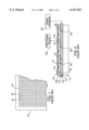
- FIG. 1 is a partial top plan view (drawn to a greatly enlarged scale) of a preferred embodiment of an active matrix electroluminescent display with which the teachings of the present invention may find more particular utility.
- FIG. 2 is a partial cross-sectional view thereof, taken along the lines 2--2 of FIG. 1, and drawn to an enlarged scale.
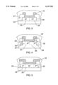
- FIG. 3 is a portion of FIG. 2, drawn to an enlarged scale, and showing the conventional respective side edges or margins of the source end of the high-voltage transistor (and in relation to the contact hole) heretofore used in the prior art.
- FIG. 4 corresponds substantially to FIG. 3, but shows (schematically) the high voltage device improvement of the present invention, wherein a P+ region is being extended from each side edge of the high-voltage transistor source, and wherein the contact hole will straddle the N+ regions and engages the respective extended P+ regions.
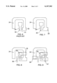
- FIG. 5 is another cross-sectional schematic view taken along the lines 5--5 of FIG. 12, and showing the completed arrangement of FIG. 4.
- FIG. 6 is a schematic plan view of the high-voltage (blocking) transistor and the low-voltage pixel access transistor used in the prior art.
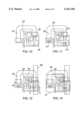
- FIGS. 7-13 are further schematic plan views, showing a preferred embodiment of the progressive steps in the masking and doping process used in the present invention. and in each view, the dark lines indicate the addition to the previous structure.
- FIG. 7 shows the modifications made to the silicon island layer to implement the improved transistors.
- FIG. 8 shows, schematically, the addition of the gates for the high-voltage and low-voltage devices.
- FIG. 9 shows, schematically, the further addition of the highly-doped regions forming the N+ source and drain of the high-voltage transistor.
- FIG. 10 shows, schematically, the implanting and penetration of the P+ regions.
- FIG. 11 shows, schematically, the formation of the respective contact holes.
- FIG. 12 shows, schematically, the metal deposition for various electrical connection purposes (as hereinafter described).
- FIG. 13 shows, schematically, the addition of the via and the EL electrode.
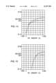
- FIG. l4 is graphics plot, showing the subthreshold characteristic of the high-voltage transistor used in the prior art.
- FIG. 15 is a further graphics plot, corresponding substantially to FIG. 14, but showing the subthreshold characteristic of the high-voltage transistor in accordance with the improvements of the present invention.
- the active matrix electroluminescent (AMEL) display 10 includes a base substrate 11, a first insulator layer 12 and a silicon layer 13 forming a silicon-on-insulator (SOI) structure.
- the base substrate 11 may be silicon, glass or quartz; the first insulator 12 is typically silicon dioxide, and the silicon layer 13 has the active semi-conductor circuits formed thereon.
- An array of metal pixel electrodes 14 is formed on a second insulator layer 15. Each pixel electrode 14 is connected to an associated electronics circuit (formed on the silicon layer 13) through a contact hole 16 etched through the second insulator layer 15.
- An electroluminescent stack 17 includes a bottom insulator layer 18, an electroluminescent layer 19 (typically of phosphor) and a top insulator layer 20 formed over the pixel electrodes 14 and the exposed surfaces of the second insulator layer 15.
- a transparent conductive layer 21 is formed over the top insulator layer 20 of the electroluminescent display 17.
- This transparent conductive layer 21, which may be an indium tin oxide (ITO) layer, receives a high voltage (either AC or DC) from a high-voltage source 22.
- a display generator 23 triggers an electronic circuit (on the silicon layer 13) to selectively activate its associated pixel electrode 14. This produces a potential gradient between the pixel electrode 14 and the transparent conductive layer 21 to illuminate the electroluminescent display 17.
- the associated electronic circuitry on the silicon layer 13 includes a high-voltage (blocking) transistor 24, a section of which is illustrated in FIG. 3, comprising an N+ region 25 and a P+ region 26 at the source, respectively, and these regions 25, 26 have respective margins or side edges 27 and 28.
- the high-voltage transistor 24 is connected to its associated pixel electrode 14 through the contact hole 16.
- a metal deposit 16A within contact hole 16 serves as a data line between pixels 14 and connects the N+ and P+ regions of the source.
- P+ region 29 and P+ region 30 are extended from the respective side edges 27 and 28 of the high-voltage transistor 24 and the contact hole 16' has been enlarged to straddle the N+ region 25 and overlap the extended P+ region 29 and, optionally, the P+ region 30 or vice versa.
- portions of the N+ region 25 may be modified to become P+ regions, thus not requiring the N+ region to be extended.
- the nominal threshold voltage of the high-voltage transistor is raised for a sharp or abrupt cut-off.
- the high-voltage transistor 24 shares a division line or connector (indicated by the broken line 31) with the low-voltage transistor 32.
- the portion 33 of the high-voltage transistor 24 is too narrow; and as a result, there will not be a sufficient amount of P+ region to still have the N+ region align with the contact hole.
- the portion 34 of the low-voltage access transistor 32 is too wide (relatively speaking) and thus the edges are not under direct gate control. As a result, there is a tendency for leakage and there is additional capacitance, which is undesirable.
- the portion 33' of the high-voltage transistor 24 has been enlarged, while the portion 34' of the low-voltage transistor 32 has been narrowed.
- a gate 35 has been provided for the high-voltage transistor 24 and a gate 36 for the low-voltage transistor 32.
- a highly-doped region 37 has been provided to form the N+ source and drain of the high-voltage transistor.
- the P+ region 39 has been implanted and allowed to penetrate.
- the process well-known in the art, involves the high-energy injection of positively-charged species which penetrate to a certain depth.
- this part of the mask is larger than the "island" to accommodate manufacturing tolerances.
- the numeral 40 indicates the common source for the low voltage and high voltage devices (as will be understood by those skilled in the art).
- the contact holes are formed (as indicated by the darkened areas 41, 42 and 43, respectively).
- the process adds metal simultaneously for a number of purposes: first, for a later via to the EL electrode (illustrated schematically as region 44); second, to connect the low-voltage drain to the high-voltage gate and tie the P+ edges of the N+ source of the HV device (illustrated schematically as region 45); and third, to attach the sources of all respective pixels to the data line (illustrated schematically as region 46).
- the present invention provides a novel high-performance pixel used, more particularly, in AMEL displays.
- the pixel combines a compact, mesa-isolated PMOS access transistor with a novel, area-efficient HV device.
- the high voltage transistor features a P+ region at each end of the source to effectively eliminate the parasitic sidewall component, raise the effective threshold voltage and reduce sensitivity to substrate potential variations.
- the improved design enhances pixel response, increases operating margins and contrast and may reduce power dissipation in the off-state.
Abstract
A high performance pixel is described for active matrix electronic displays. The pixel combines a compact, mesa-isolated PMOS access transistor with a novel, area-efficient HV device. The high voltage transistor features a P+ region at each end of the source to effectively eliminate the parasitic sidewall component and raise the nominal threshold voltage. Concurrently, excess well area is eliminated from the PMOS access transistor to minimize device leakage and the undesirable capacitance component. The improved design enhances pixel response, increases operating margins and contrast and may reduce power dissipation in the off-state.
Description
This invention is related to the field of active matrix electronic displays, for example, an active matrix electroluminescent (AMEL) display used in head-mounted displays (HMD) because of their inherent lightweight, compactness and rugged qualities as well as low-power requirements; and more particularly, to an active matrix electroluminescent display having a plurality of high-performance pixels.
In a typical AMEL display, a plurality of metal pixel electrodes are formed as "islands" in a layer insulated from a silicon-on-oxide (SOI) structure in which the active semi-conductor circuits are formed. These semi-conductor circuits are connected to the pixel electrodes through respective contact holes formed in the insulated layer. An electroluminescent (EL) stack is formed over the pixel electrodes; and this EL stack is a "sandwich" of EL material, typically phosphor, between top and bottom insulated layers. A transparent conductive layer, which receives the high voltage source, is provided on top of the EL stack; and this entire thin-film structure is on a base or substrate formed of silicon, glass, quartz or other suitable material.
In operation, a low-voltage transistor controls a high-voltage (blocking) transistor; and the high-voltage transistor turns on and "addresses" its associated pixel to illuminate the adjacent (or proximate) electroluminescent material in response to a signal received via a common pixel electrode, the signal being in the order of 100 to 400 volts (AC or DC).
Such an overall arrangement is disclosed in my earlier patent, U.S. Pat. No. 5,485,055 issued on Jan. 16, 1996 and assigned to the assignee of the present invention; moreover, in this '055 patent, the array of pixel electrodes has a uniformly textured surface for an enhanced brightness of the display.
The prior art includes the following publications (of which I am a co-author):
11.3: High-Resolution Active-Matrix Electroluminescent Display SID 94 DIGEST 137
42.3: A 1280×1024 Active-Matrix EL Display SID 95 DIGEST 891
24.3: A 2000-Ipi Active-Matrix EL Display 374 SID 96 DIGEST
Other prior art, of which I am aware, are U.S. Pat. Nos. 5,302,966; 5,463,279; and 5,587,329.
In the prior art, there is an inherent problem of coupling between adjacent pixels, which detracts from the overall resolution of the display; and there is a need for improved pixel response, better contrast and increased operating margins.
The present invention will be described in terms applicable to an AMEL for illustrative purposes only and is not intended to limit the applicability of the invention.
The present invention finds utility in an active matrix display wherein at least one controlling access transistor and one NMOS high voltage blocking transistor, having a source with an N+ region and a P+ region both terminating in respective side edges and a drain connected to the pixel electrode, are formed in a semiconducting material and wherein parasitic leakage currents develop along the respective device edges during operation.
In accordance with the teachings of the present invention, a P+ region is formed to coincide with the side edge of the N+ region or alternatively, P+ regions are formed to coincide along both edges of the high voltage device source to remove the parasitic sidewall transistor component, reduce sensitivity to substrate potential variations, facilitate an abrupt turn-off and raise the effective threshold voltage. For example, P+ regions may be added to the one or both of the side edges of the high voltage device or alternatively, the existing N+ region may be modified so that a portion of the N+ region becomes P+. Preferably, the well area of the access transistor is minimized to eliminate drain-source leakage and reduce undesirable capacitive coupling effects in the storage node. Implementation of the devices eliminates pixel coupling and enhances resolution, response and contrast.
Preferably, the contact hole to the HV device source is enlarged to enable electrical connection of the N+ and the extended P+ region or alternatively, both P+ regions. However, equivalent results can be obtained by connecting the regions by other means, for example by using a self-aligned silicide procedure which places a conductive layer selectively over the entire source region of the device. Comparable results may conceivably be achieved by contacting the N+ exclusively or by contacting the N+ and one of the P+ regions.
It is recognized that incremental improvements in pixel performance could be realized by implementing either one as well as both of the enhanced semiconductor devices or by reversing the polarity of one or both of the semiconductor devices, for example by implementing a high voltage PMOS transistor instead of the NMOS transistor. In such case, the source area would consist of a primary P+ region with N+ edge regions and the drain would consist of a P type region.
In a preferred embodiment, the electroluminescent (EL) display is an active matrix electroluminescent (AMEL) display, and the high-voltage transistor is formed on a silicon-on-insulator (SOI) thin film.
In accordance with the further teachings of the present invention, the high voltage and access transistors are placed within the pixel boundaries to conserve area and maximize array density and resolution.
These and other objects of the present invention will become apparent from a reading of the following specification taken in conjunction with the enclosed drawings.
FIG. 1 is a partial top plan view (drawn to a greatly enlarged scale) of a preferred embodiment of an active matrix electroluminescent display with which the teachings of the present invention may find more particular utility.
FIG. 2 is a partial cross-sectional view thereof, taken along the lines 2--2 of FIG. 1, and drawn to an enlarged scale.
FIG. 3 is a portion of FIG. 2, drawn to an enlarged scale, and showing the conventional respective side edges or margins of the source end of the high-voltage transistor (and in relation to the contact hole) heretofore used in the prior art.
FIG. 4 corresponds substantially to FIG. 3, but shows (schematically) the high voltage device improvement of the present invention, wherein a P+ region is being extended from each side edge of the high-voltage transistor source, and wherein the contact hole will straddle the N+ regions and engages the respective extended P+ regions.
FIG. 5 is another cross-sectional schematic view taken along the lines 5--5 of FIG. 12, and showing the completed arrangement of FIG. 4.
FIG. 6 is a schematic plan view of the high-voltage (blocking) transistor and the low-voltage pixel access transistor used in the prior art.
FIGS. 7-13 are further schematic plan views, showing a preferred embodiment of the progressive steps in the masking and doping process used in the present invention; and in each view, the dark lines indicate the addition to the previous structure.
FIG. 7 shows the modifications made to the silicon island layer to implement the improved transistors.
FIG. 8 shows, schematically, the addition of the gates for the high-voltage and low-voltage devices.
FIG. 9 shows, schematically, the further addition of the highly-doped regions forming the N+ source and drain of the high-voltage transistor.
FIG. 10 shows, schematically, the implanting and penetration of the P+ regions.
FIG. 11 shows, schematically, the formation of the respective contact holes.
FIG. 12 shows, schematically, the metal deposition for various electrical connection purposes (as hereinafter described).
FIG. 13 shows, schematically, the addition of the via and the EL electrode.
FIG. l4 is graphics plot, showing the subthreshold characteristic of the high-voltage transistor used in the prior art.
FIG. 15 is a further graphics plot, corresponding substantially to FIG. 14, but showing the subthreshold characteristic of the high-voltage transistor in accordance with the improvements of the present invention.
With reference to FIGS. 1 and 2 (and as disclosed in my aforementioned '055 patent) the active matrix electroluminescent (AMEL) display 10 includes a base substrate 11, a first insulator layer 12 and a silicon layer 13 forming a silicon-on-insulator (SOI) structure. The base substrate 11 may be silicon, glass or quartz; the first insulator 12 is typically silicon dioxide, and the silicon layer 13 has the active semi-conductor circuits formed thereon. An array of metal pixel electrodes 14 is formed on a second insulator layer 15. Each pixel electrode 14 is connected to an associated electronics circuit (formed on the silicon layer 13) through a contact hole 16 etched through the second insulator layer 15. An electroluminescent stack 17 includes a bottom insulator layer 18, an electroluminescent layer 19 (typically of phosphor) and a top insulator layer 20 formed over the pixel electrodes 14 and the exposed surfaces of the second insulator layer 15. A transparent conductive layer 21 is formed over the top insulator layer 20 of the electroluminescent display 17. This transparent conductive layer 21, which may be an indium tin oxide (ITO) layer, receives a high voltage (either AC or DC) from a high-voltage source 22. In operation, a display generator 23 triggers an electronic circuit (on the silicon layer 13) to selectively activate its associated pixel electrode 14. This produces a potential gradient between the pixel electrode 14 and the transparent conductive layer 21 to illuminate the electroluminescent display 17.
With reference to FIG. 3, the associated electronic circuitry on the silicon layer 13 includes a high-voltage (blocking) transistor 24, a section of which is illustrated in FIG. 3, comprising an N+ region 25 and a P+ region 26 at the source, respectively, and these regions 25, 26 have respective margins or side edges 27 and 28. The high-voltage transistor 24 is connected to its associated pixel electrode 14 through the contact hole 16. A metal deposit 16A within contact hole 16 serves as a data line between pixels 14 and connects the N+ and P+ regions of the source.
With reference to FIGS. 4 and 5, and in accordance with the teachings of the present invention, P+ region 29 and P+ region 30 are extended from the respective side edges 27 and 28 of the high-voltage transistor 24 and the contact hole 16' has been enlarged to straddle the N+ region 25 and overlap the extended P+ region 29 and, optionally, the P+ region 30 or vice versa. Alternatively, portions of the N+ region 25 may be modified to become P+ regions, thus not requiring the N+ region to be extended.
As a result, the parasitic sidewall components and the coupling between adjacent pixels is effectively eliminated. As shown in FIGS. 14 and 15, the nominal threshold voltage of the high-voltage transistor is raised for a sharp or abrupt cut-off.
With reference to FIGS. 6-13, the formation of the respective extended P+ regions 29 and 30 and the further improvements of the present invention (which are illustrated schematically) will become readily apparent to those skilled in the art. Moreover, it will be appreciated that the present invention is completely compatible with the conventional doping, etching and implanting techniques of currently-available process technology.
With this in mind, and with reference to FIG. 6, the high-voltage transistor 24 shares a division line or connector (indicated by the broken line 31) with the low-voltage transistor 32. The portion 33 of the high-voltage transistor 24 is too narrow; and as a result, there will not be a sufficient amount of P+ region to still have the N+ region align with the contact hole. Additionally, the portion 34 of the low-voltage access transistor 32 is too wide (relatively speaking) and thus the edges are not under direct gate control. As a result, there is a tendency for leakage and there is additional capacitance, which is undesirable.
Accordingly, and as shown in FIG. 7, the portion 33' of the high-voltage transistor 24 has been enlarged, while the portion 34' of the low-voltage transistor 32 has been narrowed.
Next, and as shown in FIG. 8, a gate 35 has been provided for the high-voltage transistor 24 and a gate 36 for the low-voltage transistor 32.
In FIG. 9, a highly-doped region 37 has been provided to form the N+ source and drain of the high-voltage transistor.
With reference to FIG. 10, the P+ region 39 has been implanted and allowed to penetrate. The process, well-known in the art, involves the high-energy injection of positively-charged species which penetrate to a certain depth. As will be noted by the darkened lines of the P+ region 39, this part of the mask is larger than the "island" to accommodate manufacturing tolerances. Moreover, in FIG. 10, the numeral 40 indicates the common source for the low voltage and high voltage devices (as will be understood by those skilled in the art).
Thereafter, and as shown in FIG. 11, the contact holes are formed (as indicated by the darkened areas 41, 42 and 43, respectively).
In FIG. 12, the process adds metal simultaneously for a number of purposes: first, for a later via to the EL electrode (illustrated schematically as region 44); second, to connect the low-voltage drain to the high-voltage gate and tie the P+ edges of the N+ source of the HV device (illustrated schematically as region 45); and third, to attach the sources of all respective pixels to the data line (illustrated schematically as region 46).
Finally, the via and EL electrode 14 are provided as shown in FIG. 13.
Accordingly, it will be appreciated that the present invention provides a novel high-performance pixel used, more particularly, in AMEL displays. The pixel combines a compact, mesa-isolated PMOS access transistor with a novel, area-efficient HV device. The high voltage transistor features a P+ region at each end of the source to effectively eliminate the parasitic sidewall component, raise the effective threshold voltage and reduce sensitivity to substrate potential variations. The improved design enhances pixel response, increases operating margins and contrast and may reduce power dissipation in the off-state.
Obviously, many modifications may be made without departing from the basic spirit of the present invention. Accordingly, it will be appreciated by those skilled in the art that within the scope of the appended claims, the invention may be practiced other than has been specifically described herein.
Claims (10)
1. An electronic display having at least one high-voltage transistor electrically connected to a pixel electrode and having a source comprising an N+ region having a first and second side edge, said first edge coincident with a side edge of a first P+ region and said source further comprising a second P+ region having a side edge coincident with said N+ second side edge.
2. The display of claim 1, wherein the electronic display is an active matrix electroluminescent display.
3. The display of claim 1, wherein the high-voltage transistor is formed on a silicon-on-insulator (SOI) thin film.
4. The display of claim 1, wherein a contact hole is provided for electrically connecting the high-voltage to a data line, and the N+ region is coincident with the contact hole.
5. The display of claim 4, wherein the contact hole is coincident with at least one of the P+ regions of the high-voltage transistor.
6. An electronic display having at least one high-voltage transistor electrically connected to a pixel electrode and having a source comprising a P+ region having a first and second side edge, said first edge coincident with a side edge of a first N+ region and said source further comprising a second N+ region coincident with said P+ second side edge.
7. The display of claim 6, wherein the electronic display is an active matrix electroluminescent (AMEL) display.
8. The display of claim 6 wherein the high-voltage transistor is formed on a silicon-on-insulator (SOI) thin film.
9. The display of claim 6, wherein a contact hole is provided for electrically connecting the high-voltage transistor to a data line, and the P+ region is coincident with the contact hole.
10. The display of claim 9, wherein the contact hole is coincident with at least one of the N+ regions of the high-voltage transistor.
Priority Applications (7)
| Application Number | Priority Date | Filing Date | Title |
|---|---|---|---|
| US08/819,413 US6147362A (en) | 1997-03-17 | 1997-03-17 | High performance display pixel for electronics displays |
| JP54056998A JP2002515139A (en) | 1997-03-17 | 1998-03-09 | High performance display pixels for electronic display |
| AT98911526T ATE228721T1 (en) | 1997-03-17 | 1998-03-09 | HIGH PERFORMANCE DISPLAY PIXELS FOR ELECTRONIC DISPLAYS |
| PCT/US1998/004562 WO1998042027A1 (en) | 1997-03-17 | 1998-03-09 | High performance display pixel for electronic displays |
| EP98911526A EP0968533B1 (en) | 1997-03-17 | 1998-03-09 | High performance display pixel for electronic displays |
| DE69809723T DE69809723T2 (en) | 1997-03-17 | 1998-03-09 | HIGH PERFORMANCE DISPLAY PIXELS FOR ELECTRONIC DISPLAY DEVICES |
| AU65463/98A AU6546398A (en) | 1997-03-17 | 1998-03-09 | High performance display pixel for electronic displays |
Applications Claiming Priority (1)
| Application Number | Priority Date | Filing Date | Title |
|---|---|---|---|
| US08/819,413 US6147362A (en) | 1997-03-17 | 1997-03-17 | High performance display pixel for electronics displays |
Publications (1)
| Publication Number | Publication Date |
|---|---|
| US6147362A true US6147362A (en) | 2000-11-14 |
Family
ID=25228087
Family Applications (1)
| Application Number | Title | Priority Date | Filing Date |
|---|---|---|---|
| US08/819,413 Expired - Lifetime US6147362A (en) | 1997-03-17 | 1997-03-17 | High performance display pixel for electronics displays |
Country Status (7)
| Country | Link |
|---|---|
| US (1) | US6147362A (en) |
| EP (1) | EP0968533B1 (en) |
| JP (1) | JP2002515139A (en) |
| AT (1) | ATE228721T1 (en) |
| AU (1) | AU6546398A (en) |
| DE (1) | DE69809723T2 (en) |
| WO (1) | WO1998042027A1 (en) |
Cited By (9)
| Publication number | Priority date | Publication date | Assignee | Title |
|---|---|---|---|---|
| US6639281B2 (en) | 2001-04-10 | 2003-10-28 | Sarnoff Corporation | Method and apparatus for providing a high-performance active matrix pixel using organic thin-film transistors |
| US20040135207A1 (en) * | 2003-01-09 | 2004-07-15 | Taner Dosluoglu | CMOS pixel with dual gate PMOS |
| US20050162070A1 (en) * | 2003-12-29 | 2005-07-28 | Lg. Philips Lcd Co., Ltd | Organic electro luminescence device |
| US20070242276A1 (en) * | 2006-04-18 | 2007-10-18 | Honeywell International, Inc. | Optical resonator gyro with external cavity beam generator |
| US20070263224A1 (en) * | 2006-05-15 | 2007-11-15 | Honeywell International, Inc. | Integrated optical rotation sensor and method for sensing rotation rate |
| US7362443B2 (en) | 2005-11-17 | 2008-04-22 | Honeywell International Inc. | Optical gyro with free space resonator and method for sensing inertial rotation rate |
| US7454102B2 (en) | 2006-04-26 | 2008-11-18 | Honeywell International Inc. | Optical coupling structure |
| US7672558B2 (en) | 2004-01-12 | 2010-03-02 | Honeywell International, Inc. | Silicon optical device |
| US11436990B2 (en) | 2019-07-18 | 2022-09-06 | Tcl China Star Optoelectronics Technology Co., Ltd. | GOA device and gate driving circuit |
Families Citing this family (1)
| Publication number | Priority date | Publication date | Assignee | Title |
|---|---|---|---|---|
| JP2007001349A (en) * | 2005-06-21 | 2007-01-11 | Inoac Corp | Lighting system for vehicle, and lighting system body for vehicle |
Citations (7)
| Publication number | Priority date | Publication date | Assignee | Title |
|---|---|---|---|---|
| US5125007A (en) * | 1988-11-25 | 1992-06-23 | Mitsubishi Denki Kabushiki Kaisha | Thin-film soi-mosfet with a body region |
| US5235195A (en) * | 1990-08-08 | 1993-08-10 | Minnesota Mining And Manufacturing Company | Solid state electromagnetic radiation detector with planarization layer |
| US5302966A (en) * | 1992-06-02 | 1994-04-12 | David Sarnoff Research Center, Inc. | Active matrix electroluminescent display and method of operation |
| US5359219A (en) * | 1992-12-04 | 1994-10-25 | Texas Instruments Incorporated | Silicon on insulator device comprising improved substrate doping |
| US5463279A (en) * | 1994-08-19 | 1995-10-31 | Planar Systems, Inc. | Active matrix electroluminescent cell design |
| US5489792A (en) * | 1994-04-07 | 1996-02-06 | Regents Of The University Of California | Silicon-on-insulator transistors having improved current characteristics and reduced electrostatic discharge susceptibility |
| US5587329A (en) * | 1994-08-24 | 1996-12-24 | David Sarnoff Research Center, Inc. | Method for fabricating a switching transistor having a capacitive network proximate a drift region |
Family Cites Families (3)
| Publication number | Priority date | Publication date | Assignee | Title |
|---|---|---|---|---|
| US3890632A (en) * | 1973-12-03 | 1975-06-17 | Rca Corp | Stabilized semiconductor devices and method of making same |
| US4345265A (en) * | 1980-04-14 | 1982-08-17 | Supertex, Inc. | MOS Power transistor with improved high-voltage capability |
| JPH0783119B2 (en) * | 1988-08-25 | 1995-09-06 | 日本電気株式会社 | Field effect transistor |
-
1997
- 1997-03-17 US US08/819,413 patent/US6147362A/en not_active Expired - Lifetime
-
1998
- 1998-03-09 WO PCT/US1998/004562 patent/WO1998042027A1/en not_active Application Discontinuation
- 1998-03-09 DE DE69809723T patent/DE69809723T2/en not_active Expired - Fee Related
- 1998-03-09 JP JP54056998A patent/JP2002515139A/en active Pending
- 1998-03-09 AU AU65463/98A patent/AU6546398A/en not_active Abandoned
- 1998-03-09 AT AT98911526T patent/ATE228721T1/en not_active IP Right Cessation
- 1998-03-09 EP EP98911526A patent/EP0968533B1/en not_active Expired - Lifetime
Patent Citations (7)
| Publication number | Priority date | Publication date | Assignee | Title |
|---|---|---|---|---|
| US5125007A (en) * | 1988-11-25 | 1992-06-23 | Mitsubishi Denki Kabushiki Kaisha | Thin-film soi-mosfet with a body region |
| US5235195A (en) * | 1990-08-08 | 1993-08-10 | Minnesota Mining And Manufacturing Company | Solid state electromagnetic radiation detector with planarization layer |
| US5302966A (en) * | 1992-06-02 | 1994-04-12 | David Sarnoff Research Center, Inc. | Active matrix electroluminescent display and method of operation |
| US5359219A (en) * | 1992-12-04 | 1994-10-25 | Texas Instruments Incorporated | Silicon on insulator device comprising improved substrate doping |
| US5489792A (en) * | 1994-04-07 | 1996-02-06 | Regents Of The University Of California | Silicon-on-insulator transistors having improved current characteristics and reduced electrostatic discharge susceptibility |
| US5463279A (en) * | 1994-08-19 | 1995-10-31 | Planar Systems, Inc. | Active matrix electroluminescent cell design |
| US5587329A (en) * | 1994-08-24 | 1996-12-24 | David Sarnoff Research Center, Inc. | Method for fabricating a switching transistor having a capacitive network proximate a drift region |
Non-Patent Citations (6)
| Title |
|---|
| A 1280 × 1024 Active-Matrix EL Display-R. Khormaei et al.; SID 95 Digest--pp. 891-893, 1995. |
| A 1280 1024 Active Matrix EL Display R. Khormaei et al.; SID 95 Digest pp. 891 893, 1995. * |
| A 2000 1pi Active Matrix EL Display, L. Arbuthnot et al.; SID 96 Digest pp. 374 377, 1996. * |
| A 2000-1pi Active-Matrix EL Display, L. Arbuthnot et al.; SID 96 Digest--pp. 374-377, 1996. |
| High Resolution Active Marix Electroluminescent Display; R. Kormaei et al.; SID 94 Digest pp. 137 139, 1994. * |
| High-Resolution Active-Marix Electroluminescent Display; R. Kormaei et al.; SID 94 Digest--pp. 137-139, 1994. |
Cited By (19)
| Publication number | Priority date | Publication date | Assignee | Title |
|---|---|---|---|---|
| US6639281B2 (en) | 2001-04-10 | 2003-10-28 | Sarnoff Corporation | Method and apparatus for providing a high-performance active matrix pixel using organic thin-film transistors |
| US7238993B2 (en) | 2003-01-09 | 2007-07-03 | Dialog Imaging Systems Gmbh | CMOS pixel with dual gate PMOS |
| US20050156212A1 (en) * | 2003-01-09 | 2005-07-21 | Dialog Semiconductor Gmbh | CMOS pixel with dual gate PMOS |
| US7336530B2 (en) | 2003-01-09 | 2008-02-26 | Digital Imaging Systems Gmbh | CMOS pixel with dual gate PMOS |
| US20050156214A1 (en) * | 2003-01-09 | 2005-07-21 | Dialog Semiconductor Gmbh | CMOS pixel with dual gate PMOS |
| US6870209B2 (en) | 2003-01-09 | 2005-03-22 | Dialog Semiconductor Gmbh | CMOS pixel with dual gate PMOS |
| US7109537B2 (en) | 2003-01-09 | 2006-09-19 | Dialog Imaging Systems Gmbh | CMOS pixel with dual gate PMOS |
| US20060278905A1 (en) * | 2003-01-09 | 2006-12-14 | Dialog Imaging Systems Gmbh | CMOS pixel with dual gate PMOS |
| US20040135207A1 (en) * | 2003-01-09 | 2004-07-15 | Taner Dosluoglu | CMOS pixel with dual gate PMOS |
| US20050162070A1 (en) * | 2003-12-29 | 2005-07-28 | Lg. Philips Lcd Co., Ltd | Organic electro luminescence device |
| US7312568B2 (en) * | 2003-12-29 | 2007-12-25 | Lg.Philips Lcd Co., Ltd. | Organic electro luminescence device having TFT with protrusions |
| US7672558B2 (en) | 2004-01-12 | 2010-03-02 | Honeywell International, Inc. | Silicon optical device |
| US7362443B2 (en) | 2005-11-17 | 2008-04-22 | Honeywell International Inc. | Optical gyro with free space resonator and method for sensing inertial rotation rate |
| US7463360B2 (en) | 2006-04-18 | 2008-12-09 | Honeywell International Inc. | Optical resonator gyro with integrated external cavity beam generator |
| US20070242276A1 (en) * | 2006-04-18 | 2007-10-18 | Honeywell International, Inc. | Optical resonator gyro with external cavity beam generator |
| US7454102B2 (en) | 2006-04-26 | 2008-11-18 | Honeywell International Inc. | Optical coupling structure |
| US20070263224A1 (en) * | 2006-05-15 | 2007-11-15 | Honeywell International, Inc. | Integrated optical rotation sensor and method for sensing rotation rate |
| US7535576B2 (en) | 2006-05-15 | 2009-05-19 | Honeywell International, Inc. | Integrated optical rotation sensor and method for sensing rotation rate |
| US11436990B2 (en) | 2019-07-18 | 2022-09-06 | Tcl China Star Optoelectronics Technology Co., Ltd. | GOA device and gate driving circuit |
Also Published As
| Publication number | Publication date |
|---|---|
| EP0968533B1 (en) | 2002-11-27 |
| EP0968533A1 (en) | 2000-01-05 |
| WO1998042027A1 (en) | 1998-09-24 |
| DE69809723T2 (en) | 2003-08-21 |
| ATE228721T1 (en) | 2002-12-15 |
| DE69809723D1 (en) | 2003-01-09 |
| JP2002515139A (en) | 2002-05-21 |
| AU6546398A (en) | 1998-10-12 |
Similar Documents
| Publication | Publication Date | Title |
|---|---|---|
| US5552615A (en) | Active matrix assembly with double layer metallization over drain contact region | |
| US6800873B2 (en) | Semiconductor device and electronic device | |
| US5365079A (en) | Thin film transistor and display device including same | |
| JP5532803B2 (en) | Semiconductor device and display device | |
| CN106992185B (en) | Thin film transistor substrate, display including the same, and method of manufacturing the same | |
| KR102565380B1 (en) | Thin film transistor substrate | |
| CN1873989B (en) | Thin film transistor and method of fabricating thin film transistor substrate | |
| EP1028471A2 (en) | Electroluminescence display device | |
| US8652885B2 (en) | Method of fabricating thin film transistor | |
| CN109817645B (en) | Array substrate, manufacturing method thereof, display panel and electronic equipment | |
| US6580127B1 (en) | High performance thin film transistor and active matrix process for flat panel displays | |
| US5981317A (en) | Method of fabricating a thin film transistor | |
| US6147362A (en) | High performance display pixel for electronics displays | |
| EP1517373B1 (en) | Flat panel display | |
| CN102013433B (en) | Organic light emitting diode display | |
| CN111415995B (en) | Display panel, manufacturing method thereof and display device | |
| US8704305B2 (en) | Thin film transistor | |
| CN109545836B (en) | OLED display device and manufacturing method thereof | |
| CN111146212B (en) | Semiconductor substrate | |
| JPH0864830A (en) | Active matrix substrate and method of fabrication thereof | |
| CN110649003A (en) | Semiconductor substrate, array substrate, inverter circuit, and switching circuit | |
| KR20000076395A (en) | High performance display pixel for electronic displays | |
| JP2022146789A (en) | thin film transistor substrate | |
| CN114582894A (en) | Array substrate and display panel | |
| KR20130074979A (en) | Method for manufacturing oxide semiconductor thin film transistor |
Legal Events
| Date | Code | Title | Description |
|---|---|---|---|
| AS | Assignment |
Owner name: ALLIEDSIGNAL INC., NEW JERSEY Free format text: ASSIGNMENT OF ASSIGNORS INTEREST;ASSIGNOR:KEYSER, THOMAS ROBERT;REEL/FRAME:008653/0508 Effective date: 19970729 |
|
| STCF | Information on status: patent grant |
Free format text: PATENTED CASE |
|
| FEPP | Fee payment procedure |
Free format text: PAYOR NUMBER ASSIGNED (ORIGINAL EVENT CODE: ASPN); ENTITY STATUS OF PATENT OWNER: LARGE ENTITY |
|
| FPAY | Fee payment |
Year of fee payment: 4 |
|
| FPAY | Fee payment |
Year of fee payment: 8 |
|
| FPAY | Fee payment |
Year of fee payment: 12 |