US6147408A - Method of forming embedded copper interconnections and embedded copper interconnection structure - Google Patents
Method of forming embedded copper interconnections and embedded copper interconnection structure Download PDFInfo
- Publication number
- US6147408A US6147408A US09/156,903 US15690398A US6147408A US 6147408 A US6147408 A US 6147408A US 15690398 A US15690398 A US 15690398A US 6147408 A US6147408 A US 6147408A
- Authority
- US
- United States
- Prior art keywords
- interconnections
- copper
- insulating layer
- embedded
- embedded copper
- Prior art date
- Legal status (The legal status is an assumption and is not a legal conclusion. Google has not performed a legal analysis and makes no representation as to the accuracy of the status listed.)
- Expired - Lifetime
Links
- 239000010949 copper Substances 0.000 title claims abstract description 74
- RYGMFSIKBFXOCR-UHFFFAOYSA-N Copper Chemical compound [Cu] RYGMFSIKBFXOCR-UHFFFAOYSA-N 0.000 title claims abstract description 69
- 229910052802 copper Inorganic materials 0.000 title claims abstract description 69
- 238000000034 method Methods 0.000 title description 10
- 230000001681 protective effect Effects 0.000 claims abstract description 34
- BQCADISMDOOEFD-UHFFFAOYSA-N Silver Chemical compound [Ag] BQCADISMDOOEFD-UHFFFAOYSA-N 0.000 claims abstract description 28
- 239000004332 silver Substances 0.000 claims abstract description 28
- 229910052709 silver Inorganic materials 0.000 claims abstract description 26
- 238000007747 plating Methods 0.000 claims abstract description 14
- 238000007654 immersion Methods 0.000 claims abstract description 13
- 238000005498 polishing Methods 0.000 claims abstract description 9
- 239000000126 substance Substances 0.000 claims abstract description 9
- 239000000758 substrate Substances 0.000 claims description 13
- 239000006104 solid solution Substances 0.000 claims description 4
- 239000010410 layer Substances 0.000 description 43
- VYPSYNLAJGMNEJ-UHFFFAOYSA-N Silicium dioxide Chemical compound O=[Si]=O VYPSYNLAJGMNEJ-UHFFFAOYSA-N 0.000 description 18
- 239000000377 silicon dioxide Substances 0.000 description 9
- 239000004065 semiconductor Substances 0.000 description 6
- 239000006023 eutectic alloy Substances 0.000 description 4
- 235000012431 wafers Nutrition 0.000 description 4
- 239000007864 aqueous solution Substances 0.000 description 3
- QVGXLLKOCUKJST-UHFFFAOYSA-N atomic oxygen Chemical compound [O] QVGXLLKOCUKJST-UHFFFAOYSA-N 0.000 description 3
- 239000000203 mixture Substances 0.000 description 3
- 239000001301 oxygen Substances 0.000 description 3
- 229910052760 oxygen Inorganic materials 0.000 description 3
- 235000012239 silicon dioxide Nutrition 0.000 description 3
- LFAGQMCIGQNPJG-UHFFFAOYSA-N silver cyanide Chemical compound [Ag+].N#[C-] LFAGQMCIGQNPJG-UHFFFAOYSA-N 0.000 description 3
- 229940098221 silver cyanide Drugs 0.000 description 3
- 229910001316 Ag alloy Inorganic materials 0.000 description 2
- 229910000881 Cu alloy Inorganic materials 0.000 description 2
- 239000007789 gas Substances 0.000 description 2
- SQGYOTSLMSWVJD-UHFFFAOYSA-N silver(1+) nitrate Chemical compound [Ag+].[O-]N(=O)=O SQGYOTSLMSWVJD-UHFFFAOYSA-N 0.000 description 2
- 229910000838 Al alloy Inorganic materials 0.000 description 1
- YCKRFDGAMUMZLT-UHFFFAOYSA-N Fluorine atom Chemical compound [F] YCKRFDGAMUMZLT-UHFFFAOYSA-N 0.000 description 1
- 238000004380 ashing Methods 0.000 description 1
- 238000010586 diagram Methods 0.000 description 1
- 238000005530 etching Methods 0.000 description 1
- 229910052731 fluorine Inorganic materials 0.000 description 1
- 239000011737 fluorine Substances 0.000 description 1
- 238000004519 manufacturing process Methods 0.000 description 1
- 239000000463 material Substances 0.000 description 1
- 230000005012 migration Effects 0.000 description 1
- 238000013508 migration Methods 0.000 description 1
- 238000012986 modification Methods 0.000 description 1
- 230000004048 modification Effects 0.000 description 1
- 239000011241 protective layer Substances 0.000 description 1
- 229910001961 silver nitrate Inorganic materials 0.000 description 1
- 239000000243 solution Substances 0.000 description 1
Images

Classifications
-
- H—ELECTRICITY
- H01—ELECTRIC ELEMENTS
- H01L—SEMICONDUCTOR DEVICES NOT COVERED BY CLASS H10
- H01L21/00—Processes or apparatus adapted for the manufacture or treatment of semiconductor or solid state devices or of parts thereof
- H01L21/70—Manufacture or treatment of devices consisting of a plurality of solid state components formed in or on a common substrate or of parts thereof; Manufacture of integrated circuit devices or of parts thereof
- H01L21/71—Manufacture of specific parts of devices defined in group H01L21/70
- H01L21/768—Applying interconnections to be used for carrying current between separate components within a device comprising conductors and dielectrics
- H01L21/76838—Applying interconnections to be used for carrying current between separate components within a device comprising conductors and dielectrics characterised by the formation and the after-treatment of the conductors
- H01L21/7684—Smoothing; Planarisation
-
- H—ELECTRICITY
- H01—ELECTRIC ELEMENTS
- H01L—SEMICONDUCTOR DEVICES NOT COVERED BY CLASS H10
- H01L21/00—Processes or apparatus adapted for the manufacture or treatment of semiconductor or solid state devices or of parts thereof
- H01L21/02—Manufacture or treatment of semiconductor devices or of parts thereof
- H01L21/04—Manufacture or treatment of semiconductor devices or of parts thereof the devices having at least one potential-jump barrier or surface barrier, e.g. PN junction, depletion layer or carrier concentration layer
- H01L21/18—Manufacture or treatment of semiconductor devices or of parts thereof the devices having at least one potential-jump barrier or surface barrier, e.g. PN junction, depletion layer or carrier concentration layer the devices having semiconductor bodies comprising elements of Group IV of the Periodic System or AIIIBV compounds with or without impurities, e.g. doping materials
- H01L21/28—Manufacture of electrodes on semiconductor bodies using processes or apparatus not provided for in groups H01L21/20 - H01L21/268
- H01L21/283—Deposition of conductive or insulating materials for electrodes conducting electric current
- H01L21/288—Deposition of conductive or insulating materials for electrodes conducting electric current from a liquid, e.g. electrolytic deposition
-
- H—ELECTRICITY
- H01—ELECTRIC ELEMENTS
- H01L—SEMICONDUCTOR DEVICES NOT COVERED BY CLASS H10
- H01L21/00—Processes or apparatus adapted for the manufacture or treatment of semiconductor or solid state devices or of parts thereof
- H01L21/70—Manufacture or treatment of devices consisting of a plurality of solid state components formed in or on a common substrate or of parts thereof; Manufacture of integrated circuit devices or of parts thereof
- H01L21/71—Manufacture of specific parts of devices defined in group H01L21/70
- H01L21/768—Applying interconnections to be used for carrying current between separate components within a device comprising conductors and dielectrics
- H01L21/76838—Applying interconnections to be used for carrying current between separate components within a device comprising conductors and dielectrics characterised by the formation and the after-treatment of the conductors
- H01L21/76886—Modifying permanently or temporarily the pattern or the conductivity of conductive members, e.g. formation of alloys, reduction of contact resistances
- H01L21/76888—By rendering at least a portion of the conductor non conductive, e.g. oxidation
-
- H—ELECTRICITY
- H01—ELECTRIC ELEMENTS
- H01L—SEMICONDUCTOR DEVICES NOT COVERED BY CLASS H10
- H01L23/00—Details of semiconductor or other solid state devices
- H01L23/52—Arrangements for conducting electric current within the device in operation from one component to another, i.e. interconnections, e.g. wires, lead frames
- H01L23/522—Arrangements for conducting electric current within the device in operation from one component to another, i.e. interconnections, e.g. wires, lead frames including external interconnections consisting of a multilayer structure of conductive and insulating layers inseparably formed on the semiconductor body
- H01L23/532—Arrangements for conducting electric current within the device in operation from one component to another, i.e. interconnections, e.g. wires, lead frames including external interconnections consisting of a multilayer structure of conductive and insulating layers inseparably formed on the semiconductor body characterised by the materials
- H01L23/53204—Conductive materials
- H01L23/53209—Conductive materials based on metals, e.g. alloys, metal silicides
- H01L23/53228—Conductive materials based on metals, e.g. alloys, metal silicides the principal metal being copper
- H01L23/53233—Copper alloys
-
- H—ELECTRICITY
- H01—ELECTRIC ELEMENTS
- H01L—SEMICONDUCTOR DEVICES NOT COVERED BY CLASS H10
- H01L2924/00—Indexing scheme for arrangements or methods for connecting or disconnecting semiconductor or solid-state bodies as covered by H01L24/00
- H01L2924/0001—Technical content checked by a classifier
- H01L2924/0002—Not covered by any one of groups H01L24/00, H01L24/00 and H01L2224/00
Definitions
- the present invention relates to a method of forming embedded interconnections of copper on a surface of a substrate such as a semiconductor wafer, and a structure of such embedded interconnections of copper.
- interconnections for use in semiconductor devices.
- embedded interconnections of copper produced by a damascene process and such embedded interconnections of copper arranged in multiple layers are employed.
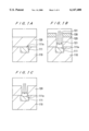
- FIGS. 1A through 1C of the accompanying drawings illustrate a process of successive steps of forming multilayer embedded interconnections of copper.
- an interconnection 111 of copper is embedded in the upper surface of an insulating layer 110 of silicon dioxide (SiO 2 ).
- Another insulating layer 120 of silicon dioxide (SiO 2 ) is disposed on the insulating layer 110 and the interconnections 111 for insulating the interconnections of copper (Cu) 111 in an upper layer.
- an exposed upper surface 111a of the interconnections 111 is undesirably oxidized by oxygen.
- an etchant (etching gas) is applied to etch the insulating layer 120 through a hole 131 defined in a resist layer pattern 130 on the surface of the insulating layer 120 for thereby forming a hole 121 in the insulating layer 120, which will be filled with a plug for connection to the interconnections 111.
- etching gas etching gas
- the exposed upper surface 111a of the interconnections 111 is undesirably oxidized by the applied oxygen.
- Another object of the present invention is to provide an embedded copper interconnection structure.
- a method of forming embedded interconnections of copper comprises the steps of: forming an insulating layer; forming embedded interconnections of copper in the insulating layer; planarizing (making coplanar) an exposed surface of the insulating layer including an exposed surface of the embedded interconnections of copper; and forming a protective film of silver on the exposed surface of the embedded interconnections of copper.
- the protective film of silver on the embedded interconnections of copper prevents the embedded interconnections of copper from being oxidized and prevents the surface thereof from being modified.
- the exposed surface of the embedded interconnections of copper may be plated with silver according to immersion plating.
- the immersion plating allows the protective film of silver to be selectively formed only on the exposed surface of the embedded interconnections of copper, and also allows the protective film of silver to be formed in a very small thickness. Therefore, the amount of silver in the protective silver film may be relatively small. Since the protective film of silver and the embedded interconnections of copper do not form a solid solution, the electrical resistance of the embedded interconnections remains relatively low even if silver and copper are diffused in each other.
- an embedded copper interconnection structure comprises a substrate, a first insulating layer disposed on the substrate, an embedded interconnection of copper disposed in the first insulating layer, a protective film of silver disposed on the embedded interconnections of copper in the first insulating layer.
- the structure also includes a second insulating layer disposed on a surface of the first insulating layer including the embedded interconnections of copper having the protective film of silver thereon.
- FIGS. 1A through 1C are fragmentary cross-sectional views showing a conventional process of successive steps of forming multilayer embedded interconnections of copper;
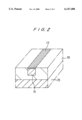
- FIG. 2 is a perspective view illustrative of a process of forming a protective film of silver (Ag) on interconnections of copper disposed in the surface of an insulating layer of SiO 2 according to the present invention
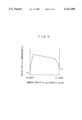
- FIG. 3 is a diagram showing the relationship between the composition of a eutectic alloy of copper and silver and the resistivity at a certain temperature
- FIGS. 4A through 4D are fragmentary cross-sectional views showing the manner in which the protective film operates.
- interconnections 15 of copper are formed by plating so as to be embedded in the surface of an insulating layer 10 of SiO 2 on the surface of a semiconductor wafer (or substrate) 25.
- the entire upper surface of the insulating layer 10 including the exposed upper surface of the interconnections 15 is made planar by chemical mechanical polishing (CMP) (the upper surface being defined as t he surface facing away from the substrate).
- CMP chemical mechanical polishing
- the semiconductor wafer is then dipped in an aqueous solution of silver cyanide to plate only the exposed surface of the interconnections 15 with a thin protective film 17 of silver (Ag) according to immersion plating.
- the protective film 17 is shown exaggerated as having an appreciably large thickness in FIG. 2, although it has a very small actual thickness on the exposed upper surface of the interconnections 15.
- the immersion plating for forming the protective film 17 is carried out according to the following formula: ##EQU1##
- the silver cyanide reacts only with the copper of the interconnections 15, but not with the silicon dioxide of the insulating layer 10. Therefore, during the immersion plating, the protective film 17 is selectively formed only on the exposed upper surface of the interconnections 15.
- the immersion plating allows the protective film 17 to be formed in a very small thickness, and may require only a relatively small amount of silver for the protective film 17.
- FIG. 3 shows the relationship between compositions of a eutectic alloy of copper and silver, which do not form a solid solution, and the resistivity at a certain temperature T 0 . It can be seen from FIG. 3 that if the concentration of copper in the eutectic alloy is close to 100% (point ⁇ B ), then the resistance of the eutectic alloy is substantially the same small value as if the concentration of copper is 100%. Therefore, since the protective film 17 is very thin and contains a relatively small amount of silver, the overall resistance of the interconnections 15 remains essentially unchanged even if silver and copper diffuse in each other.
- a second insulating layer 20 of SiO 2 is formed on the first insulating layer 10, including the first layer of interconnections 15 and the protective film 17, for supporting interconnections of copper in an upper layer.
- the protective film 17 prevents the interconnections 15 from being oxidized.
- a resist layer 30 is formed on the upper surface of the insulating layer 20. Then an etchant of fluorine gas is applied to the insulating layer 20 through a hole 31 defined in the resist layer 30 for forming a hole 21 in the insulating layer 20, which will be filled with a plug 15 for connection to the interconnections 15. At this time, the etchant contacts the protective film 17, but not the interconnections 15. Therefore, the interconnection 15 is prevented from being modified by the etchant.
- the resist layer 30 shown in FIG. 4B is then oxidized and removed by ashing, as shown in FIG. 4C. At this time, the protective film 17 prevents the interconnections 15 from being oxidized.
- one embodiment of the present invention includes a plurality of insulating layers 10, 20, formed on a substrate 25.
- Each of the insulating layers 10, 20 has embedded interconnections of copper 15, 36.
- a protective film of silver 17, 37, is formed on each of the embedded interconnections of copper.
- each of the insulating layers is planarized by chemical mechanical polishing.
- they may be planarized by any of various planarizing processes other than chemical mechanical polishing.
- aqueous solution of silver cyanide is employed in the immersion plating process in the above embodiment
- another solution such as an aqueous solution of silver nitrate may be employed in immersion plating.
- the present invention offers the following advantages.
- the protective film of Ag on the exposed upper surface of the interconnections of Cu prevents the interconnections from being oxidized or modified. Therefore, the yield of the semiconductor devices will be improved, and the production throughput of semiconductor wafers will be increased.
- the protective film of Ag is formed on the exposed upper surface of the interconnections of Cu by immersion plating, the protective film of Ag can be selectively formed only on the exposed surface of the interconnections of Cu without a mask.
- the protective film can have a very small thickness, which will reduce the amount of Ag that diffuses in the Cu interconnections. Hence, the electrical resistance of the interconnections will be prevented from increasing.
Abstract
Embedded interconnections of copper are formed by forming insulating layer, forming an embedded interconnections of copper in the insulating layer, making an exposed upper surface of the insulating layer and an exposed surface of the embedded interconnections of copper coplanar according to chemical mechanical polishing, and forming a protective silver film on the exposed surface of the embedded interconnections of copper. These steps are repeated on the existing insulating layer thereby to produce multiple layers of embedded interconnections of copper. The exposed surface of the embedded interconnections of copper is plated with silver according to immersion plating.
Description
1. Field of the Invention
The present invention relates to a method of forming embedded interconnections of copper on a surface of a substrate such as a semiconductor wafer, and a structure of such embedded interconnections of copper.
2. Description of the Related Art
Generally, aluminum alloys have heretofore been used as the materials of interconnections for use in semiconductor devices. For lower electric resistance and greater migration resistance, however, embedded interconnections of copper produced by a damascene process, and such embedded interconnections of copper arranged in multiple layers are employed.
Conventional multilayer embedded interconnections of copper have suffered various problems. Such problems will be described below with reference to FIGS. 1A through 1C of the accompanying drawings which illustrate a process of successive steps of forming multilayer embedded interconnections of copper.
As shown in FIG. 1A, an interconnection 111 of copper is embedded in the upper surface of an insulating layer 110 of silicon dioxide (SiO2). Another insulating layer 120 of silicon dioxide (SiO2) is disposed on the insulating layer 110 and the interconnections 111 for insulating the interconnections of copper (Cu) 111 in an upper layer. When the insulating layer 120 is deposited on the interconnections layer 111, an exposed upper surface 111a of the interconnections 111 is undesirably oxidized by oxygen.
As shown in FIG. 1B, an etchant (etching gas) is applied to etch the insulating layer 120 through a hole 131 defined in a resist layer pattern 130 on the surface of the insulating layer 120 for thereby forming a hole 121 in the insulating layer 120, which will be filled with a plug for connection to the interconnections 111. When the insulating layer 120 is thus etched, the exposed upper surface 111a of the interconnections 111 is undesirably modified in the composition by the etchant.
As shown in FIG. 1C, when the resist layer 130 (see FIG. 1B) is removed using oxygen, the exposed upper surface 111a of the interconnections 111 is undesirably oxidized by the applied oxygen.
It is therefore an object of the present invention to provide a method of forming embedded interconnections of copper while effectively preventing an exposed surface of an the interconnections of copper from being modified or oxidized.
Another object of the present invention is to provide an embedded copper interconnection structure.
According to the present invention, a method of forming embedded interconnections of copper/comprises the steps of: forming an insulating layer; forming embedded interconnections of copper in the insulating layer; planarizing (making coplanar) an exposed surface of the insulating layer including an exposed surface of the embedded interconnections of copper; and forming a protective film of silver on the exposed surface of the embedded interconnections of copper. The protective film of silver on the embedded interconnections of copper prevents the embedded interconnections of copper from being oxidized and prevents the surface thereof from being modified.
To form the protective film of silver on the exposed surface of the embedded interconnections of copper, the exposed surface of the embedded interconnections of copper may be plated with silver according to immersion plating. The immersion plating allows the protective film of silver to be selectively formed only on the exposed surface of the embedded interconnections of copper, and also allows the protective film of silver to be formed in a very small thickness. Therefore, the amount of silver in the protective silver film may be relatively small. Since the protective film of silver and the embedded interconnections of copper do not form a solid solution, the electrical resistance of the embedded interconnections remains relatively low even if silver and copper are diffused in each other.
According to the present invention, an embedded copper interconnection structure comprises a substrate, a first insulating layer disposed on the substrate, an embedded interconnection of copper disposed in the first insulating layer, a protective film of silver disposed on the embedded interconnections of copper in the first insulating layer. The structure also includes a second insulating layer disposed on a surface of the first insulating layer including the embedded interconnections of copper having the protective film of silver thereon.
The above and other objects, features, and advantages of the present invention will become apparent from the following description when taken in conjunction with the accompanying drawings which illustrate a preferred embodiment of the present invention by way of example.
FIGS. 1A through 1C are fragmentary cross-sectional views showing a conventional process of successive steps of forming multilayer embedded interconnections of copper;
FIG. 2 is a perspective view illustrative of a process of forming a protective film of silver (Ag) on interconnections of copper disposed in the surface of an insulating layer of SiO2 according to the present invention;
FIG. 3 is a diagram showing the relationship between the composition of a eutectic alloy of copper and silver and the resistivity at a certain temperature;
FIGS. 4A through 4D are fragmentary cross-sectional views showing the manner in which the protective film operates.
As shown in FIG. 2, interconnections 15 of copper are formed by plating so as to be embedded in the surface of an insulating layer 10 of SiO2 on the surface of a semiconductor wafer (or substrate) 25. The entire upper surface of the insulating layer 10 including the exposed upper surface of the interconnections 15 is made planar by chemical mechanical polishing (CMP) (the upper surface being defined as t he surface facing away from the substrate). The semiconductor wafer is then dipped in an aqueous solution of silver cyanide to plate only the exposed surface of the interconnections 15 with a thin protective film 17 of silver (Ag) according to immersion plating. The protective film 17 is shown exaggerated as having an appreciably large thickness in FIG. 2, although it has a very small actual thickness on the exposed upper surface of the interconnections 15.
The immersion plating for forming the protective film 17 is carried out according to the following formula: ##EQU1##
The silver cyanide reacts only with the copper of the interconnections 15, but not with the silicon dioxide of the insulating layer 10. Therefore, during the immersion plating, the protective film 17 is selectively formed only on the exposed upper surface of the interconnections 15.
The immersion plating allows the protective film 17 to be formed in a very small thickness, and may require only a relatively small amount of silver for the protective film 17.
FIG. 3 shows the relationship between compositions of a eutectic alloy of copper and silver, which do not form a solid solution, and the resistivity at a certain temperature T0. It can be seen from FIG. 3 that if the concentration of copper in the eutectic alloy is close to 100% (point ρB), then the resistance of the eutectic alloy is substantially the same small value as if the concentration of copper is 100%. Therefore, since the protective film 17 is very thin and contains a relatively small amount of silver, the overall resistance of the interconnections 15 remains essentially unchanged even if silver and copper diffuse in each other.
As shown in FIG. 4A, a second insulating layer 20 of SiO2 is formed on the first insulating layer 10, including the first layer of interconnections 15 and the protective film 17, for supporting interconnections of copper in an upper layer. At this time, the protective film 17 prevents the interconnections 15 from being oxidized.
As shown in FIG. 4B, a resist layer 30 is formed on the upper surface of the insulating layer 20. Then an etchant of fluorine gas is applied to the insulating layer 20 through a hole 31 defined in the resist layer 30 for forming a hole 21 in the insulating layer 20, which will be filled with a plug 15 for connection to the interconnections 15. At this time, the etchant contacts the protective film 17, but not the interconnections 15. Therefore, the interconnection 15 is prevented from being modified by the etchant.
The resist layer 30 shown in FIG. 4B is then oxidized and removed by ashing, as shown in FIG. 4C. At this time, the protective film 17 prevents the interconnections 15 from being oxidized.
After a plug 35 is formed in the hole 21 in the insulating layer 20 and a second layer of interconnections 36 is embedded in the insulating layer 20, the overall surface of the insulating layer 20 is planarized by chemical mechanical polishing. If another insulating layer of SiO2 is to be formed on the planarized insulating layer 20, then a protective layer of Ag 37 may be formed on the exposed upper surface of the next interconnections 36 by immersion plating. Thus, as shown in FIG. 4D, one embodiment of the present invention includes a plurality of insulating layers 10, 20, formed on a substrate 25. Each of the insulating layers 10, 20 has embedded interconnections of copper 15, 36. A protective film of silver 17, 37, is formed on each of the embedded interconnections of copper.
In the above embodiment, the overall upper surface of each of the insulating layers is planarized by chemical mechanical polishing. However, they may be planarized by any of various planarizing processes other than chemical mechanical polishing.
While the aqueous solution of silver cyanide is employed in the immersion plating process in the above embodiment, another solution such as an aqueous solution of silver nitrate may be employed in immersion plating.
The present invention offers the following advantages. The protective film of Ag on the exposed upper surface of the interconnections of Cu prevents the interconnections from being oxidized or modified. Therefore, the yield of the semiconductor devices will be improved, and the production throughput of semiconductor wafers will be increased.
Because the protective film of Ag is formed on the exposed upper surface of the interconnections of Cu by immersion plating, the protective film of Ag can be selectively formed only on the exposed surface of the interconnections of Cu without a mask. The protective film can have a very small thickness, which will reduce the amount of Ag that diffuses in the Cu interconnections. Hence, the electrical resistance of the interconnections will be prevented from increasing.
Although a certain preferred embodiment of the present invention has been shown and described in detail, it should be understood that various changes and modifications may be made therein without departing from the scope of the appended claims.
Claims (9)
1. An embedded copper interconnection structure comprising:
a substrate having an upper surface;
an insulating layer disposed on said substrate so as to cover substantially all of said upper surface of said substrate, said insulating layer having embedded copper interconnections and an upper surface, each of said embedded copper interconnections having an exposed upper surface; and
a protective silver film formed on said exposed upper surface of each of said embedded copper interconnections by immersion plating.
2. The copper interconnection structure of claim 1, wherein said upper surface of said insulating layer and said exposed upper surface of each of said embedded copper interconnections are formed to be coplanar by chemical mechanical polishing.
3. The copper interconnection structure of claim 1, wherein said protective silver film is formed after said chemical mechanical polishing.
4. The copper interconnection structure of claim 1, wherein said protective silver film has a small thickness and is free of a solid solution having copper.
5. The copper interconnection structure of claim 1, wherein said insulating layer comprises a first insulating layer and said embedded copper interconnections comprise first embedded copper interconnections, further comprising a second insulating layer disposed on said first insulating layer and said first embedded copper interconnections, said second insulating layer having second embedded copper interconnections, said second insulating layer having holes for establishing connections between said first embedded copper interconnections and said second embedded copper interconnections.
6. A multilayer embedded copper interconnection structure comprising:
a substrate having an upper surface;
a plurality of insulating layers disposed in succession on said substrate, said plurality of insulating layers including a first insulating layer disposed on said substrate so as to cover substantially all of said upper surface of said substrate, each of said insulating layers having embedded copper interconnections and an upper surface, each of said embedded copper interconnections having an exposed upper surface; and
a protective silver film formed on said exposed upper surface of each of said respective embedded copper interconnections by immersion plating.
7. The multilayer copper interconnection structure of claim 6, wherein said upper surface of each of said plurality of insulating layers and said exposed upper surface of each of said respective embedded copper interconnections are formed to be coplanar by chemical mechanical polishing.
8. The multilayer copper interconnection structure of claim 6, wherein said protective silver film is formed after said chemical mechanical polishing.
9. The multilayer copper interconnection structure of claim 6, wherein said protective silver film has a small thickness and is free of a solid solution having copper.
Priority Applications (2)
| Application Number | Priority Date | Filing Date | Title |
|---|---|---|---|
| US09/660,411 US6391775B1 (en) | 1997-09-18 | 2000-09-12 | Method of forming embedded copper interconnections and embedded copper interconnection structure |
| US10/118,228 US6787467B2 (en) | 1997-09-18 | 2002-04-09 | Method of forming embedded copper interconnections and embedded copper interconnection structure |
Applications Claiming Priority (2)
| Application Number | Priority Date | Filing Date | Title |
|---|---|---|---|
| JP27200197A JP3545177B2 (en) | 1997-09-18 | 1997-09-18 | Method for forming multilayer embedded Cu wiring |
| JP9-272001 | 1997-09-18 |
Related Child Applications (1)
| Application Number | Title | Priority Date | Filing Date |
|---|---|---|---|
| US09/660,411 Division US6391775B1 (en) | 1997-09-18 | 2000-09-12 | Method of forming embedded copper interconnections and embedded copper interconnection structure |
Publications (1)
| Publication Number | Publication Date |
|---|---|
| US6147408A true US6147408A (en) | 2000-11-14 |
Family
ID=17507772
Family Applications (3)
| Application Number | Title | Priority Date | Filing Date |
|---|---|---|---|
| US09/156,903 Expired - Lifetime US6147408A (en) | 1997-09-18 | 1998-09-18 | Method of forming embedded copper interconnections and embedded copper interconnection structure |
| US09/660,411 Expired - Fee Related US6391775B1 (en) | 1997-09-18 | 2000-09-12 | Method of forming embedded copper interconnections and embedded copper interconnection structure |
| US10/118,228 Expired - Lifetime US6787467B2 (en) | 1997-09-18 | 2002-04-09 | Method of forming embedded copper interconnections and embedded copper interconnection structure |
Family Applications After (2)
| Application Number | Title | Priority Date | Filing Date |
|---|---|---|---|
| US09/660,411 Expired - Fee Related US6391775B1 (en) | 1997-09-18 | 2000-09-12 | Method of forming embedded copper interconnections and embedded copper interconnection structure |
| US10/118,228 Expired - Lifetime US6787467B2 (en) | 1997-09-18 | 2002-04-09 | Method of forming embedded copper interconnections and embedded copper interconnection structure |
Country Status (5)
| Country | Link |
|---|---|
| US (3) | US6147408A (en) |
| EP (2) | EP1471572A1 (en) |
| JP (1) | JP3545177B2 (en) |
| KR (1) | KR100555931B1 (en) |
| DE (1) | DE69829716T2 (en) |
Cited By (12)
| Publication number | Priority date | Publication date | Assignee | Title |
|---|---|---|---|---|
| US6444567B1 (en) * | 2000-01-05 | 2002-09-03 | Advanced Micro Devices, Inc. | Process for alloying damascene-type Cu interconnect lines |
| US6455424B1 (en) * | 2000-08-07 | 2002-09-24 | Micron Technology, Inc. | Selective cap layers over recessed polysilicon plugs |
| US20030075808A1 (en) * | 2001-08-13 | 2003-04-24 | Hiroaki Inoue | Semiconductor device, method for manufacturing the same, and plating solution |
| US20030193056A1 (en) * | 2002-03-26 | 2003-10-16 | Semiconductor Energy Laboratory Co., Ltd. | Light-emitting device, liquid-crystal display device and method for manufacturing same |
| US20030228749A1 (en) * | 2002-06-06 | 2003-12-11 | Nishant Sinha | Plating metal caps on conductive interconnect for wirebonding |
| US20040004289A1 (en) * | 2002-07-04 | 2004-01-08 | Kazuyoshi Ueno | Semiconductor device and manufacturing method thereof |
| US6696761B2 (en) * | 1998-11-20 | 2004-02-24 | Chartered Semiconductor Manufacturing Ltd. | Method to encapsulate copper plug for interconnect metallization |
| US20050090098A1 (en) * | 2003-10-27 | 2005-04-28 | Dubin Valery M. | Method for making a semiconductor device having increased conductive material reliability |
| US20050285987A1 (en) * | 2004-06-23 | 2005-12-29 | Sharp Kabushiki Kaisha | Active matrix substrate and manufacturing method thereof, and electronic device |
| US20090035936A1 (en) * | 2007-07-31 | 2009-02-05 | Juergen Boemmels | Semiconductor device having a grain orientation layer |
| US20120013011A1 (en) * | 2010-07-14 | 2012-01-19 | Roland Hampp | Conductive Lines and Pads and Method of Manufacturing Thereof |
| US20150325511A1 (en) * | 2013-03-14 | 2015-11-12 | UTAC Headquarters Pte. Ltd. | Semiconductor packages and methods of packaging semiconductor devices |
Families Citing this family (3)
| Publication number | Priority date | Publication date | Assignee | Title |
|---|---|---|---|---|
| US6709971B2 (en) * | 2002-01-30 | 2004-03-23 | Intel Corporation | Interconnect structures in a semiconductor device and processes of formation |
| US7268074B2 (en) * | 2004-06-14 | 2007-09-11 | Enthone, Inc. | Capping of metal interconnects in integrated circuit electronic devices |
| WO2006095990A1 (en) * | 2005-03-11 | 2006-09-14 | Lg Chem, Ltd. | An lcd device having a silver capped electrode |
Citations (8)
| Publication number | Priority date | Publication date | Assignee | Title |
|---|---|---|---|---|
| US4922321A (en) * | 1986-01-27 | 1990-05-01 | Mitsubishi Denki Kabushiki Kaisha | Semiconductor device and a method of producing same |
| US4996584A (en) * | 1985-01-31 | 1991-02-26 | Gould, Inc. | Thin-film electrical connections for integrated circuits |
| US5071518A (en) * | 1989-10-24 | 1991-12-10 | Microelectronics And Computer Technology Corporation | Method of making an electrical multilayer interconnect |
| US5250120A (en) * | 1990-12-07 | 1993-10-05 | Kanegafuchi Chemical Industry Co., Ltd. | Photovoltaic device |
| JPH066012A (en) * | 1992-06-16 | 1994-01-14 | Ebara Corp | Coating structure for electric circuit |
| US5406120A (en) * | 1992-10-20 | 1995-04-11 | Jones; Robert M. | Hermetically sealed semiconductor ceramic package |
| US5545927A (en) * | 1995-05-12 | 1996-08-13 | International Business Machines Corporation | Capped copper electrical interconnects |
| US5891802A (en) * | 1997-07-23 | 1999-04-06 | Advanced Micro Devices, Inc. | Method for fabricating a metallization stack structure to improve electromigration resistance and keep low resistivity of ULSI interconnects |
Family Cites Families (19)
| Publication number | Priority date | Publication date | Assignee | Title |
|---|---|---|---|---|
| US4619887A (en) * | 1985-09-13 | 1986-10-28 | Texas Instruments Incorporated | Method of plating an interconnect metal onto a metal in VLSI devices |
| JPS63100749A (en) * | 1986-10-17 | 1988-05-02 | Hitachi Ltd | Semiconductor integrated circuit device |
| JP2624703B2 (en) * | 1987-09-24 | 1997-06-25 | 株式会社東芝 | Method and apparatus for forming bump |
| US5098860A (en) | 1990-05-07 | 1992-03-24 | The Boeing Company | Method of fabricating high-density interconnect structures having tantalum/tantalum oxide layers |
| JP2609940B2 (en) * | 1990-06-22 | 1997-05-14 | 鐘淵化学工業株式会社 | Multilayer wiring body |
| US5300813A (en) * | 1992-02-26 | 1994-04-05 | International Business Machines Corporation | Refractory metal capped low resistivity metal conductor lines and vias |
| JP3049161B2 (en) * | 1992-11-18 | 2000-06-05 | イビデン株式会社 | Method for manufacturing multi-chip thin film multilayer wiring board |
| DE4400200C2 (en) * | 1993-01-05 | 1997-09-04 | Toshiba Kawasaki Kk | Semiconductor device with improved wiring structure and method of manufacturing the same |
| JPH08148563A (en) * | 1994-11-22 | 1996-06-07 | Nec Corp | Formation of multilayer wiring structure body of semiconductor device |
| US5549808A (en) | 1995-05-12 | 1996-08-27 | International Business Machines Corporation | Method for forming capped copper electrical interconnects |
| US5674787A (en) * | 1996-01-16 | 1997-10-07 | Sematech, Inc. | Selective electroless copper deposited interconnect plugs for ULSI applications |
| US5913147A (en) | 1997-01-21 | 1999-06-15 | Advanced Micro Devices, Inc. | Method for fabricating copper-aluminum metallization |
| US5939334A (en) * | 1997-05-22 | 1999-08-17 | Sharp Laboratories Of America, Inc. | System and method of selectively cleaning copper substrate surfaces, in-situ, to remove copper oxides |
| US6069068A (en) | 1997-05-30 | 2000-05-30 | International Business Machines Corporation | Sub-quarter-micron copper interconnections with improved electromigration resistance and reduced defect sensitivity |
| US6214728B1 (en) * | 1998-11-20 | 2001-04-10 | Chartered Semiconductor Manufacturing, Ltd. | Method to encapsulate copper plug for interconnect metallization |
| US6309964B1 (en) | 1999-07-08 | 2001-10-30 | Taiwan Semiconductor Manufacturing Company | Method for forming a copper damascene structure over tungsten plugs with improved adhesion, oxidation resistance, and diffusion barrier properties using nitridation of the tungsten plug |
| US6114243A (en) * | 1999-11-15 | 2000-09-05 | Chartered Semiconductor Manufacturing Ltd | Method to avoid copper contamination on the sidewall of a via or a dual damascene structure |
| US6274499B1 (en) * | 1999-11-19 | 2001-08-14 | Chartered Semiconductor Manufacturing Ltd. | Method to avoid copper contamination during copper etching and CMP |
| US6291082B1 (en) * | 2000-06-13 | 2001-09-18 | Advanced Micro Devices, Inc. | Method of electroless ag layer formation for cu interconnects |
-
1997
- 1997-09-18 JP JP27200197A patent/JP3545177B2/en not_active Expired - Fee Related
-
1998
- 1998-09-17 KR KR1019980038367A patent/KR100555931B1/en not_active IP Right Cessation
- 1998-09-18 EP EP20040018231 patent/EP1471572A1/en not_active Withdrawn
- 1998-09-18 US US09/156,903 patent/US6147408A/en not_active Expired - Lifetime
- 1998-09-18 DE DE69829716T patent/DE69829716T2/en not_active Expired - Fee Related
- 1998-09-18 EP EP98117790A patent/EP0903781B1/en not_active Expired - Lifetime
-
2000
- 2000-09-12 US US09/660,411 patent/US6391775B1/en not_active Expired - Fee Related
-
2002
- 2002-04-09 US US10/118,228 patent/US6787467B2/en not_active Expired - Lifetime
Patent Citations (8)
| Publication number | Priority date | Publication date | Assignee | Title |
|---|---|---|---|---|
| US4996584A (en) * | 1985-01-31 | 1991-02-26 | Gould, Inc. | Thin-film electrical connections for integrated circuits |
| US4922321A (en) * | 1986-01-27 | 1990-05-01 | Mitsubishi Denki Kabushiki Kaisha | Semiconductor device and a method of producing same |
| US5071518A (en) * | 1989-10-24 | 1991-12-10 | Microelectronics And Computer Technology Corporation | Method of making an electrical multilayer interconnect |
| US5250120A (en) * | 1990-12-07 | 1993-10-05 | Kanegafuchi Chemical Industry Co., Ltd. | Photovoltaic device |
| JPH066012A (en) * | 1992-06-16 | 1994-01-14 | Ebara Corp | Coating structure for electric circuit |
| US5406120A (en) * | 1992-10-20 | 1995-04-11 | Jones; Robert M. | Hermetically sealed semiconductor ceramic package |
| US5545927A (en) * | 1995-05-12 | 1996-08-13 | International Business Machines Corporation | Capped copper electrical interconnects |
| US5891802A (en) * | 1997-07-23 | 1999-04-06 | Advanced Micro Devices, Inc. | Method for fabricating a metallization stack structure to improve electromigration resistance and keep low resistivity of ULSI interconnects |
Cited By (31)
| Publication number | Priority date | Publication date | Assignee | Title |
|---|---|---|---|---|
| US6696761B2 (en) * | 1998-11-20 | 2004-02-24 | Chartered Semiconductor Manufacturing Ltd. | Method to encapsulate copper plug for interconnect metallization |
| US6444567B1 (en) * | 2000-01-05 | 2002-09-03 | Advanced Micro Devices, Inc. | Process for alloying damascene-type Cu interconnect lines |
| US7078755B2 (en) | 2000-08-07 | 2006-07-18 | Micron Technology, Inc. | Memory cell with selective deposition of refractory metals |
| US20020179956A1 (en) * | 2000-08-07 | 2002-12-05 | Mcteer Allen | Memory cell with selective deposition of refractory metals |
| US20070012987A1 (en) * | 2000-08-07 | 2007-01-18 | Mcteer Allen | Memory cell with selective deposition of refractory metals |
| US6455424B1 (en) * | 2000-08-07 | 2002-09-24 | Micron Technology, Inc. | Selective cap layers over recessed polysilicon plugs |
| US20060040487A1 (en) * | 2001-08-13 | 2006-02-23 | Hiroaki Inoue | Semiconductor device, method for manufacturing the same, and plating solution |
| US7279408B2 (en) | 2001-08-13 | 2007-10-09 | Ebara Corporation | Semiconductor device, method for manufacturing the same, and plating solution |
| US20080011228A1 (en) * | 2001-08-13 | 2008-01-17 | Hiroaki Inoue | Semiconductor device, method for manufacturing the same, and plating solution |
| US7060618B2 (en) * | 2001-08-13 | 2006-06-13 | Ebara Corporation | Semiconductor device, method for manufacturing the same, and plating solution |
| US20030075808A1 (en) * | 2001-08-13 | 2003-04-24 | Hiroaki Inoue | Semiconductor device, method for manufacturing the same, and plating solution |
| US7935967B2 (en) | 2002-03-26 | 2011-05-03 | Semiconductor Energy Laboratory Co., Ltd. | Light-emitting device, liquid-crystal display device and method for manufacturing same |
| US7045861B2 (en) | 2002-03-26 | 2006-05-16 | Semiconductor Energy Laboratory Co., Ltd. | Light-emitting device, liquid-crystal display device and method for manufacturing same |
| US20060186441A1 (en) * | 2002-03-26 | 2006-08-24 | Semiconductor Energy Laboratory Co., Ltd. | Light-emitting device, liquid-crystal display device and method for manufacturing same |
| US20030193056A1 (en) * | 2002-03-26 | 2003-10-16 | Semiconductor Energy Laboratory Co., Ltd. | Light-emitting device, liquid-crystal display device and method for manufacturing same |
| US8293552B2 (en) | 2002-03-26 | 2012-10-23 | Semiconductor Energy Laboratory Co., Ltd. | Light-emitting device, liquid-crystal display device and method for manufacturing same |
| US20030228749A1 (en) * | 2002-06-06 | 2003-12-11 | Nishant Sinha | Plating metal caps on conductive interconnect for wirebonding |
| US20040157433A1 (en) * | 2002-06-06 | 2004-08-12 | Nishant Sinha | Plating metal caps on conductive interconnect for wirebonding |
| US20040004289A1 (en) * | 2002-07-04 | 2004-01-08 | Kazuyoshi Ueno | Semiconductor device and manufacturing method thereof |
| US7332813B2 (en) * | 2002-07-04 | 2008-02-19 | Nec Electronics Corporation | Semiconductor device |
| US7229922B2 (en) * | 2003-10-27 | 2007-06-12 | Intel Corporation | Method for making a semiconductor device having increased conductive material reliability |
| US20050090098A1 (en) * | 2003-10-27 | 2005-04-28 | Dubin Valery M. | Method for making a semiconductor device having increased conductive material reliability |
| US20050285987A1 (en) * | 2004-06-23 | 2005-12-29 | Sharp Kabushiki Kaisha | Active matrix substrate and manufacturing method thereof, and electronic device |
| US7547918B2 (en) | 2004-06-23 | 2009-06-16 | Sharp Kabushiki Kaisha | Active matrix substrate and electronic device |
| US20090035936A1 (en) * | 2007-07-31 | 2009-02-05 | Juergen Boemmels | Semiconductor device having a grain orientation layer |
| US8404577B2 (en) * | 2007-07-31 | 2013-03-26 | Globalfoundries Inc. | Semiconductor device having a grain orientation layer |
| US20120013011A1 (en) * | 2010-07-14 | 2012-01-19 | Roland Hampp | Conductive Lines and Pads and Method of Manufacturing Thereof |
| US8586472B2 (en) * | 2010-07-14 | 2013-11-19 | Infineon Technologies Ag | Conductive lines and pads and method of manufacturing thereof |
| US9006898B2 (en) | 2010-07-14 | 2015-04-14 | Infineon Technologies Ag | Conductive lines and pads and method of manufacturing thereof |
| US20150325511A1 (en) * | 2013-03-14 | 2015-11-12 | UTAC Headquarters Pte. Ltd. | Semiconductor packages and methods of packaging semiconductor devices |
| US9786625B2 (en) * | 2013-03-14 | 2017-10-10 | United Test And Assembly Center Ltd. | Semiconductor packages and methods of packaging semiconductor devices |
Also Published As
| Publication number | Publication date |
|---|---|
| EP0903781A2 (en) | 1999-03-24 |
| EP0903781A3 (en) | 1999-07-21 |
| JP3545177B2 (en) | 2004-07-21 |
| EP0903781B1 (en) | 2005-04-13 |
| DE69829716T2 (en) | 2006-03-09 |
| US6787467B2 (en) | 2004-09-07 |
| DE69829716D1 (en) | 2005-05-19 |
| JPH1197441A (en) | 1999-04-09 |
| US20020111022A1 (en) | 2002-08-15 |
| EP1471572A1 (en) | 2004-10-27 |
| US6391775B1 (en) | 2002-05-21 |
| KR100555931B1 (en) | 2006-05-03 |
| KR19990029869A (en) | 1999-04-26 |
Similar Documents
| Publication | Publication Date | Title |
|---|---|---|
| US6153521A (en) | Metallized interconnection structure and method of making the same | |
| US4789648A (en) | Method for producing coplanar multi-level metal/insulator films on a substrate and for forming patterned conductive lines simultaneously with stud vias | |
| US6147408A (en) | Method of forming embedded copper interconnections and embedded copper interconnection structure | |
| US5783483A (en) | Method of fabricating a barrier against metal diffusion | |
| US20020036309A1 (en) | Semiconductor device and method for fabricating the same | |
| US20020024142A1 (en) | Semiconductor device and manufacturing method of the same | |
| US6020266A (en) | Single step electroplating process for interconnect via fill and metal line patterning | |
| US5055426A (en) | Method for forming a multilevel interconnect structure on a semiconductor wafer | |
| JPH04290232A (en) | Formation method of groove-buried interconnection | |
| TWI413188B (en) | Conductive line structure and the method of forming the same | |
| EP0628998B1 (en) | Wiring layer for semi conductor device and method for manufacturing the same | |
| US6346472B1 (en) | Manufacturing method for semiconductor metalization barrier | |
| JP2001053077A (en) | Semiconductor integrated circuit device and its manufacture | |
| JPS62298136A (en) | Manufacture of semiconductor element | |
| KR100458594B1 (en) | Fabrication method of semiconductor device | |
| KR20030056157A (en) | Fabrication method of semiconductor device | |
| JP2005142330A (en) | Semiconductor device and method of manufacturing same | |
| KR20030049029A (en) | Fabrication method of semiconductor device | |
| KR0171016B1 (en) | Metal-wiring method of semiconductor device | |
| KR100315035B1 (en) | Metal wiring formation method of semiconductor device | |
| JPS636847A (en) | Manufacture of semiconductor device | |
| JPH06232124A (en) | Manufacture of semiconductor device | |
| KR20000015238A (en) | Method for forming a metal wire of a semiconductor device | |
| KR20060031179A (en) | Method of forming copper interconnection of semiconductor device | |
| KR20050005961A (en) | method for forming metal line in semiconductor device |
Legal Events
| Date | Code | Title | Description |
|---|---|---|---|
| AS | Assignment |
Owner name: EBARA CORPORATION, JAPAN Free format text: ASSIGNMENT OF ASSIGNORS INTEREST;ASSIGNORS:OGURE, NAOAKI;INOUE, HIROKI;REEL/FRAME:009626/0319 Effective date: 19981022 |
|
| STCF | Information on status: patent grant |
Free format text: PATENTED CASE |
|
| FEPP | Fee payment procedure |
Free format text: PAYOR NUMBER ASSIGNED (ORIGINAL EVENT CODE: ASPN); ENTITY STATUS OF PATENT OWNER: LARGE ENTITY |
|
| FPAY | Fee payment |
Year of fee payment: 4 |
|
| FPAY | Fee payment |
Year of fee payment: 8 |
|
| FPAY | Fee payment |
Year of fee payment: 12 |