US6147664A - Controlling the brightness of an FED device using PWM on the row side and AM on the column side - Google Patents
Controlling the brightness of an FED device using PWM on the row side and AM on the column side Download PDFInfo
- Publication number
- US6147664A US6147664A US09/164,402 US16440298A US6147664A US 6147664 A US6147664 A US 6147664A US 16440298 A US16440298 A US 16440298A US 6147664 A US6147664 A US 6147664A
- Authority
- US
- United States
- Prior art keywords
- row
- brightness
- screen
- fed
- column
- Prior art date
- Legal status (The legal status is an assumption and is not a legal conclusion. Google has not performed a legal analysis and makes no representation as to the accuracy of the status listed.)
- Expired - Lifetime
Links
Images

Classifications
-
- G—PHYSICS
- G09—EDUCATION; CRYPTOGRAPHY; DISPLAY; ADVERTISING; SEALS
- G09G—ARRANGEMENTS OR CIRCUITS FOR CONTROL OF INDICATING DEVICES USING STATIC MEANS TO PRESENT VARIABLE INFORMATION
- G09G3/00—Control arrangements or circuits, of interest only in connection with visual indicators other than cathode-ray tubes
- G09G3/20—Control arrangements or circuits, of interest only in connection with visual indicators other than cathode-ray tubes for presentation of an assembly of a number of characters, e.g. a page, by composing the assembly by combination of individual elements arranged in a matrix no fixed position being assigned to or needed to be assigned to the individual characters or partial characters
- G09G3/22—Control arrangements or circuits, of interest only in connection with visual indicators other than cathode-ray tubes for presentation of an assembly of a number of characters, e.g. a page, by composing the assembly by combination of individual elements arranged in a matrix no fixed position being assigned to or needed to be assigned to the individual characters or partial characters using controlled light sources
-
- G—PHYSICS
- G09—EDUCATION; CRYPTOGRAPHY; DISPLAY; ADVERTISING; SEALS
- G09G—ARRANGEMENTS OR CIRCUITS FOR CONTROL OF INDICATING DEVICES USING STATIC MEANS TO PRESENT VARIABLE INFORMATION
- G09G2310/00—Command of the display device
- G09G2310/02—Addressing, scanning or driving the display screen or processing steps related thereto
- G09G2310/0264—Details of driving circuits
- G09G2310/0267—Details of drivers for scan electrodes, other than drivers for liquid crystal, plasma or OLED displays
-
- G—PHYSICS
- G09—EDUCATION; CRYPTOGRAPHY; DISPLAY; ADVERTISING; SEALS
- G09G—ARRANGEMENTS OR CIRCUITS FOR CONTROL OF INDICATING DEVICES USING STATIC MEANS TO PRESENT VARIABLE INFORMATION
- G09G2320/00—Control of display operating conditions
- G09G2320/04—Maintaining the quality of display appearance
- G09G2320/043—Preventing or counteracting the effects of ageing
-
- G—PHYSICS
- G09—EDUCATION; CRYPTOGRAPHY; DISPLAY; ADVERTISING; SEALS
- G09G—ARRANGEMENTS OR CIRCUITS FOR CONTROL OF INDICATING DEVICES USING STATIC MEANS TO PRESENT VARIABLE INFORMATION
- G09G2320/00—Control of display operating conditions
- G09G2320/06—Adjustment of display parameters
- G09G2320/0606—Manual adjustment
-
- G—PHYSICS
- G09—EDUCATION; CRYPTOGRAPHY; DISPLAY; ADVERTISING; SEALS
- G09G—ARRANGEMENTS OR CIRCUITS FOR CONTROL OF INDICATING DEVICES USING STATIC MEANS TO PRESENT VARIABLE INFORMATION
- G09G2320/00—Control of display operating conditions
- G09G2320/06—Adjustment of display parameters
- G09G2320/0626—Adjustment of display parameters for control of overall brightness
-
- G—PHYSICS
- G09—EDUCATION; CRYPTOGRAPHY; DISPLAY; ADVERTISING; SEALS
- G09G—ARRANGEMENTS OR CIRCUITS FOR CONTROL OF INDICATING DEVICES USING STATIC MEANS TO PRESENT VARIABLE INFORMATION
- G09G3/00—Control arrangements or circuits, of interest only in connection with visual indicators other than cathode-ray tubes
- G09G3/20—Control arrangements or circuits, of interest only in connection with visual indicators other than cathode-ray tubes for presentation of an assembly of a number of characters, e.g. a page, by composing the assembly by combination of individual elements arranged in a matrix no fixed position being assigned to or needed to be assigned to the individual characters or partial characters
- G09G3/2007—Display of intermediate tones
- G09G3/2011—Display of intermediate tones by amplitude modulation
-
- G—PHYSICS
- G09—EDUCATION; CRYPTOGRAPHY; DISPLAY; ADVERTISING; SEALS
- G09G—ARRANGEMENTS OR CIRCUITS FOR CONTROL OF INDICATING DEVICES USING STATIC MEANS TO PRESENT VARIABLE INFORMATION
- G09G3/00—Control arrangements or circuits, of interest only in connection with visual indicators other than cathode-ray tubes
- G09G3/20—Control arrangements or circuits, of interest only in connection with visual indicators other than cathode-ray tubes for presentation of an assembly of a number of characters, e.g. a page, by composing the assembly by combination of individual elements arranged in a matrix no fixed position being assigned to or needed to be assigned to the individual characters or partial characters
- G09G3/2007—Display of intermediate tones
- G09G3/2014—Display of intermediate tones by modulation of the duration of a single pulse during which the logic level remains constant
Definitions
- the present invention relates to the field of flat panel display screens. More specifically, the present invention relates to the field of flat panel field emission displays (FEDs).
- FEDs flat panel field emission displays
- Flat panel FED display devices also called thin CRTs, include a flat panel screen having rows and columns of intersecting lines. The lines intersect to form subpixels.
- AM amplitude modulated
- Pulse width modulation (PWM) has been proposed for gray scale generation. In low-capacitance panels and in low gray scale generation situations, this technique may have application. However, in high capacitance (e.g., about 1 pf/subpixel) panels and 256 gray scale situations, PWM is not useful and in the general case consumes too much power. In these situations, PWM has not been used generally for carrying the image data to the columns because of certain time restraints inherent in the FED screen display technique.
- the time period allotted for each column driver must be divided into at least 256 discrete time intervals. Assuming a display having 400 rows, the 1/60 sec frame update rate is divided by 400 yielding a 1/24,000 sec time frame in which all columns need to be updated.
- AM has been used in the past to adjust the brightness of a FED device.
- the operating point of the emission cathode is changed thereby possibly affecting the gamma (e.g., v-i characteristics of the subpixels) and white point balance of the display screen. It would be desirable to provide a brightness adjustment that did not affect the gamma or white balance of the display screen.
- AMLCDs Active matrix liquid crystal devices
- AMLCDs Active matrix liquid crystal devices
- the brightness adjustment of AMLCD devices alters the gray scale resolution of the pixels.
- These flat panel display screens alter the brightness of the display by controlling the electrical drive to, and hence the intensity of, the backlighting lamp.
- the color and the uniformity produced by an AMLCD device degrade as the backlighting lamp is moved away from an optimum brightness point.
- the optimum brightness point is typically factory set.
- this prior art method of altering the brightness of a flat panel display has the unfortunate side effect of degrading the quality of the displayed image. It is desirable to provide a brightness adjustment for a flat panel display screen that does not compromise the gray scale quality of the pixels.
- the image data used to render an image on the screen is altered as it is fed to the display.
- a function composed of a gain and an offset value is programmed into the display and all image data is then passed through the function which multiplies the data by the gain value and then adds the programmed offset value.
- the values of the above function are then altered as the brightness needs to be increased or decreased.
- This prior art mechanism for altering screen brightness is disadvantageous because it requires relatively complex circuitry for altering the large volume of image data.
- this prior art mechanism degrades the gray scale quality of the image by altering the gray scale resolution of the flat panel display. It is desirable to provide a brightness adjustment for a flat panel display screen that does not alter the image data nor compromise the gray scale resolution of the image.
- Flat panel field emission displays do not use backlighting lamps.
- Flat panel FEDs utilize emitters each having an anode and a cathode and a gate. The voltage applied across an individual emitter (gate to cathode) causes it to release electrons toward a phosphor spot located on a display screen. Many emitters are associated with a single phosphor spot.
- a pixel is composed of three (e.g., red, green and blue) independently controlled phosphor spots.
- the gray scale content of a pixel within a flat panel FED screen is represented by the voltages applied to the red, green and blue emitters that constitute the pixel.
- a brightness adjustment mechanism that alters the relative voltages applied to the emitters of the red, green and blue phosphor spots will vary the gray scale quality of the pixels within a flat panel FED screen. It is desirable to provide a brightness adjustment for a flat panel FED screen that does not compromise the gray scale resolution of the pixels.
- One prior art mechanism for altering the brightness of an FED alters the high voltage (e.g., several kilovolts) applied to the emitter's anode. This method is disadvantageous because it requires a variable output high voltage power supply which is more complex and hence more expensive than a constant voltage output power supply. Secondly, this prior art mechanism requires that the brightness adjustment circuitry be implemented with high voltage components rather than less expensive, simpler low voltage components. It is desirable to provide a brightness adjustment for a flat panel FED screen that does not require altering high voltage levels nor that requires high voltage components.
- the present invention provides a mechanism and method for controlling the brightness of a flat panel display screen that does not compromise the gray scale resolution of the pixels of the display screen.
- the present invention also provides a mechanism for altering the brightness of a flat panel display screen that does not alter the image data.
- the present invention also provides a mechanism for altering the brightness of a flat panel display screen that does not alter the gamma or white balance of the display screen.
- a circuit and method are described herein for controlling the brightness of a display screen implemented using a flat panel field emission display (FED) screen.
- FED flat panel field emission display
- a matrix of rows and columns is provided and emitters are situated within each row-column intersection. Rows are activated sequentially and separate gray scale information is presented to the columns. In one embodiment, rows are activated sequentially from the top most row down to the bottom row with only one row asserted at a time. Alternatively, the rows can be interlaced.
- a phosphor spot e.g., red, green, blue, causing an illumination point. Therefore, each pixel contains one red, one green and one blue phosphor spot, "subpixel.”
- the present invention utilizes amplitude modulation (AM) for gray scale generation via the column drivers and pulse width modulation (PWM) for dimming (brightness control) via the row drivers to accomplish this goal.
- AM amplitude modulation
- PWM pulse width modulation
- the row drive is by its nature a pulsed operation.
- row "on-times" are larger than 17 us (e.g., for XGA video formats)
- the rise time and drive impedances become more reasonable, especially for simultaneous panel-wide modulation.
- the row on time window is uniformly shortened in accordance with the present invention to thereby reduce the brightness of the entire screen without changing the instantaneous v-i characteristic of the driven subpixels.
- the present invention includes specialized circuitry common to all the row drivers for altering the pulse width of the enable voltage applied to the rows to cause a change in brightness cross the FED screen. Brightness is substantially linearly related to the enable pulse width.
- the applied voltage is pulse width modulated to alter the brightness of the flat panel FED screen. Because the relative column voltages remain constant within this embodiment of the present invention, gray scale resolution is not compromised as brightness is altered.
- the enable lines of the row drivers are turned on and off to modulate the pulse width ("on-time") of the row voltage.
- the row driver power supply is interrupted to modulate the pulse width ("on-time") of the row voltage. It is more efficient to alter the row voltage than the column voltage. This is the case because there is no increase in CV 2 loss with row modulation.
- embodiments of the present invention include a field emission display screen including: a plurality of column drivers for driving amplitude modulated voltage signals over a plurality of column lines wherein each column driver is coupled to a respective column line and receives image data for the respective column line; a plurality of row drivers for driving a voltage pulse over a plurality of row lines wherein each row driver is coupled to a respective row line, the plurality of row lines intersecting the plurality of column lines and wherein a subpixel is defined as an intersection of one row line and one column line; an enable circuit for enabling only one row driver at a time, the enable circuit coupled to each row driver of the plurality of row drivers; and a pulse width modulation circuit for generating the voltage pulse wherein the pulse width modulation circuit is for varying the width of the voltage pulse in order to effect brightness within the FED screen without loss of gray scale resolution capability of the FED screen.
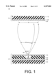
- FIG. 1 is a cross section structural view of part of a flat panel FED screen that utilizes a gated field emitter situated at the intersection of a row and a column line.
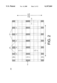
- FIG. 2 is a plan view of internal portions of the flat panel FED screen of the present invention and illustrates several intersecting rows and columns of the display.
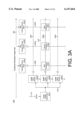
- FIG. 3A illustrates brightness control circuitry of the present invention for using PWM for the row drive and AM for the column drive within a flat panel FED screen.
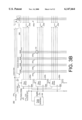
- FIG. 3B illustrates a plan view of a flat panel FED screen in accordance with the present invention illustrating row and column drivers and numerous intersecting rows and columns.
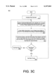
- FIG. 3C is a flow diagram illustrating steps of the process performed by the brightness control circuitry of FIG. 3A in accordance with the present invention.
- FIG. 4 is a circuit schematic illustrating circuitry utilized by the present invention for altering the brightness of the flat panel FED screen of the present invention.
- FIG. 5 illustrates timing diagrams of the signals produced by the circuit of FIG. 4 and used by the row drivers of the flat panel FED screen of FIG. 3B.
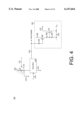
- FIG. 6 is an illustration of brightness controlled column drivers of the flat panel FED screen of the present invention.
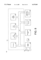
- FIG. 7 is a perspective view of a computer system utilizing an ambient light sensor in accordance with one embodiment of the present invention.
- FIG. 8 is a block diagram of circuitry of a general purpose computer system including an FED screen of the present invention having an ambient light sensor.
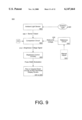
- FIG. 9 is a logical block diagram of a circuit of the present invention for utilizing an ambient light sensor for automatically adjusting the brightness of an flat panel FED screen.
- FIG. 10 is a logical block diagram of a circuit of the present invention utilizing an ambient light sensor and feed-back for automatically adjust the brightness of a flat panel FED screen for brightness normalizing.
- FIG. 1 illustrates a multi-layer structure 75 which is a portion of an FED flat panel display.
- the multi-layer structure 75 contains a field-emission backplate structure 45, also called a baseplate structure, and an electron-receiving faceplate structure 70.
- An image is generated by faceplate structure 70.
- Backplate structure 45 commonly consists of an electrically insulating backplate 65, an emitter (or cathode) electrode 60, an electrically insulating layer 55, a patterned gate electrode 50, and a conical electron-emissive element 40 situated in an aperture through insulating layer 55.
- One type of electron-emissive element 40 is described in U.S. Pat. No.
- Anode 20 of FIG. 1 is maintained at a positive voltage relative to cathode 60/40.
- the anode voltage is 100-300 volts for spacing of 100-200 um between structures 45 and 70 but in other embodiments with greater spacing the anode voltage is in the kilovolt range.
- the anode voltage is also impressed on phosphors 25.
- a suitable gate voltage is applied to gate electrode 50, electrons are emitted from electron-emissive element 40 at various values of off-normal emission angle theta 42.
- the emitted electrons follow non-linear (e.g., parabolic) trajectories indicated by lines 35 in FIG. 1 and impact on a target portion 30 of the phosphors 25.
- the phosphors struck by the emitted electrons produce light of a selected color and represent a phosphor spot.
- a single phosphor spot can be illuminated by thousands of emitters.
- Phosphors 25 are a subpixel part of a picture element ("pixel") that contains other phosphors (not shown) which emit light of different color than that produced by phosphors 25. Typically a pixel contains three phosphor spots or "subpixels," a red spot, a green spot and a blue spot. Also, the pixel containing phosphors 25 adjoins one or more other pixels (not shown) in the FED flat panel display. If some of the electrons intended for phosphors 25 consistently strike other phosphors (in the same or another pixels), the image resolution and color purity can become degraded. As discussed in more detail below, the pixels of an FED flat panel screen are arranged in a matrix form including columns and rows.
- a pixel is composed of three phosphor spots ("subpixels") aligned in the same row, but having three separate columns. Therefore, a single pixel is uniquely identified by one row and three separate columns (a red column, a green column and a blue column). In one embodiment, the total area of the three subpixels is substantially square.
- target phosphor portion 30 depends on the applied voltages and geometric and dimensional characteristics of the FED flat panel display 75. Increasing the anode/phosphor voltage to 1,500 to 10,000 volts in the FED flat panel display 75 of FIG. 1 requires that the spacing between the backplate structure 45 and the faceplate structure 70 be much greater than 100-200 um. Increasing the interstructure spacing to the value needed for a phosphor potential of 1,500 to 10,000 volts causes a larger phosphor portion 30, unless electron focusing elements (e.g., gated field emission structures) are added to the FED flat panel display of FIG. 1. Such focusing elements can be included within FED flat panel display structure 75 and are described in U.S. Pat. No. 5,528,103 issued on Jun. 18, 1996 to Spindt, et al., which is incorporated herein by reference.
- electron focusing elements e.g., gated field emission structures
- the brightness of the target phosphor portion 30 depends on the voltage potential applied across the cathode 60/40 and the gate 50. The larger the voltage potential, the brighter the target phosphor portion 30.
- the brightness of the target phosphor portion 30 depends on the amount of time a voltage is applied across the cathode 40/60 and the gate 50 (e.g., on-time window). The larger the on-time window, the brighter the target phosphor portion 30. Therefore, the brightness of FED flat panel structure 75 is dependent on the voltage and the amount of time (e.g., "on-time") the voltage is applied across cathode 60/40 and the gate 50. As discussed in more detail below, brightness is adjusted uniformly over the FED display screen by adjusting the pulse width of the on-time window for all row drivers.
- the FED flat panel display is subdivided into an array of horizontally aligned rows and vertically aligned columns of pixels.
- a portion 100 of this array is shown in FIG. 2.
- the boundaries of a respective pixel 125 are indicated by dashed lines.
- Three separate emitter lines 230 are shown.
- Each emitter line 230 is a row electrode for one of the rows of pixels in the array.
- the middle row electrode 230 is coupled to the emitter cathodes 60/40 (FIG. 1) of each emitter of the particular row associated with the electrode.
- a portion of one pixel row is indicated in FIG. 2 and is situated between a pair of adjacent spacer walls 135.
- a pixel row is comprised of all of the pixels along one row line 250.
- Each column of pixels has three gate lines 250: (1) one for red; (2) a second for green; and (3) a third for blue.
- each pixel column includes one of each phosphor stripes (red, green, blue), three stripes total.
- Each of the gate lines 250 is coupled to the gate 50 (FIG. 1) of each emitter structure of the associated column. This structure 100 is described in more detail in U.S. Pat. No. 5,477,105 issued on Dec. 19, 1995 to Curtin, et al., which is incorporated herein by reference.
- the red, green and blue phosphor stripes 25 are maintained at a positive voltage of 1,500 to 10,000 volts relative to the voltage of the emitter-electrode 60/40.
- elements 40 in that set emit electrons which are accelerated toward a target portion 30 of the phosphors in the corresponding color.
- the excited phosphors then emit light.
- a screen frame refresh cycle (performed at a rate of approximately 60 Hz in one embodiment) only one row is active at a time and the column lines are energized to illuminate the one row of pixels for the on-time period.
- FIG. 3A illustrates a blow up of circuitry used by the present invention within the FED flat panel display screen 200 to perform uniform brightness control.
- An exemplary pixel 125' is shown having three subpixels, 125f (red), 125g (green) and 125h (blue).
- the three subpixels exist within a common row line 230g and have three separate column lines 250f, 250g and 250h.
- Each column line is driven by its own column driver, 240a, 240b and 240c, respectively.
- Three row lines are shown, 230f, 230g and 230h and each row line is driven by its own row driver circuit 220a, 220b and 220c, respectively.
- AM column data is latched into the column drivers 240 and only one row is enabled (during the on-time window) at any time to update the pixels of that row. This process is performed for each row of the display screen 200.
- the AM image data is presented over data line 205 of FIG. 3A.
- a horizontal synchronization clock signal 214 synchronizes the updating of the rows.
- Clock signal 214 is fed to a pulse width generator circuit 300 which generates the pulse width of the row on-time window. Therefore, the start of each row on-time window is synchronized with the horizontal synchronization clock signal 214 and the pulse width of each on-time window is adjusted by the pulse width generator 300. Consecutive row on-time windows do not overlap in time since only one row is enabled at any time. In a typical refresh rate, the horizontal synchronization clock 214 is presented at a rate of between 15-30 us.
- the pulse width generator 300 varies the pulse width of the on-time window which acts as an enable pulse for the row drivers 220.
- the pulse width e.g., the on-time window
- the pulse width e.g., the on-time window
- Every subpixel of display 200 is effected uniformly for a change in the on-time window since each row driver 220 receives the same on-time pulse over the common enable line 216.
- the gamma and white balance and gray scale resolution of the display 200 remain unchanged because the AM signals over line 205 remain unchanged.
- the total area of the 3 subpixels 125d, 125g and 125h is substantially square in geometry.
- FIG. 3B illustrates the circuitry of the FED flat panel display screen 200 in accordance with the present invention in more detail.
- Region 100 as described with respect to FIG. 2, is also shown in FIG. 3B.
- the FED flat panel display screen 200 consists of n row lines (horizontal) and x column lines (vertical). For clarity, a row line is called a "row” and a column line is called a "column.” Row lines are driven by row driver circuits 220a-220c. Shown in FIG. 3B are row groups 230a, 230b and 230c. Each row group is associated with a particular row driver circuit; three row driver circuits are shown 220a-220c. In one embodiment of the present invention there are over 400 rows and approximately 5-10 row driver circuits.
- the present invention is equally well suited to an FED flat panel display screen having any number of rows. Also shown in FIG. 3B are column groups 250a, 250b, 250c and 250d. In one embodiment of the present invention there are over 1920 columns. However, it is appreciated that the present invention is equally well suited to an FED flat panel display screen having any number of columns. A pixel requires three columns (red, green, blue), therefore, 1920 columns provides at least 640 pixel resolution horizontally.
- Row driver circuits 220a-220c are placed along the periphery of the FED flat panel display screen 200. In FIG. 3B, only three row drivers are shown for clarity. Each row driver 220a-220c is responsible for driving a group of rows. For instance, row driver 220a drives rows 230a, row driver 220b drives rows 230b and row driver 220c drives rows 230c. Although an individual row driver is responsible for driving a group of rows, only one row is active at a time across the entire FED flat panel display screen 200. Therefore, an individual row driver drives at most one row line at a time, and when the active row line is not in its group during a refresh cycle it is not driving any row line.
- a supply voltage line 212 is coupled in parallel to all row drivers 220a-220c and supplies the row drivers with a driving voltage for application to the cathode 60/40 of the emitters. In one embodiment, the row driving voltage is negative in polarity.
- An enable signal is also supplied to each row driver 220a-220c in parallel over enable line 216 of FIG. 38.
- enable line 216 When the enable line 216 is low, all row drivers 220a-220c of FED screen 200 are disabled and no row is energized.
- the enable line 216 When the enable line 216 is high, the row drivers 220a-220c are enabled.
- a pulse width generator circuit 300 controls the enable line 216.
- a horizontal clock signal is also supplied to each row driver 220a-220c in parallel over clock line 214 of FIG. 3B.
- the horizontal clock signal or synchronization signal pulses upon each time a new row is to be energized.
- the n rows of a frame are energized, one at a time, to form a frame of data. Assuming an exemplary frame update rate of 60 Hz, all rows are updated once every 16.67 milliseconds.
- the horizontal clock signal pulses once every 16.67/n milliseconds. In other words a new row is energized every 16.67/n milliseconds. If n is 400, the horizontal clock signal pulses once every 41.67 microseconds.
- All row drivers of FED 200 are configured to implement one large serial shift register having n bits of storage, one bit per row. Row data is shifted through these row drivers using a row data line 212 that is coupled to the row drivers 220a-220c in serial fashion.
- all but one of the bits of the n bits within the row drivers contain a "0" and the other one contains a "1". Therefore, the "1" is shifted serially through all n rows, one at a time, from the upper most row to the bottom most row.
- the row corresponding to the "1" is then driven for the on-time window.
- the bits of the shift registers are shifted through the row drivers 220a-220c once every pulse of the horizontal clock as provided by line 214.
- the odd rows are updated in series followed by the even rows.
- a different bit pattern and clocking scheme is therefore used.
- the row corresponding to the shifted "1" becomes driven responsive to the horizontal clock pulse over line 214.
- the row remains on during a particular "on-time” window.
- the corresponding row is driven with the voltage value as seen over voltage supply line 212 if the row drivers are enabled.
- the other rows are not driven with any voltage.
- the present invention varies the size of the on-time window to alter the brightness of the FED flat panel display screen 200 of FIG. 3B. To increase the brightness, the on-time window is expanded. To decrease the brightness, the on-time window is decreased. Since the relative voltage amplitudes are not altered on the column drivers, the present invention does not degrade gray scale resolution by altering brightness in the above fashion.
- the rows are energized with a negative voltage.
- FIG. 38 there are three columns per pixel within the FED flat panel display screen 200 of the present invention.
- Column lines 250a control one column of pixels
- column lines 250c control another column line of pixels, etc.
- FIG. 38 also illustrates the column drivers 240 that control the gray scale information for each pixel.
- the column drivers 240 drive amplitude modulated voltage signals over the column lines.
- the column drivers 240 can be broken into separate circuits that each drive groups of column lines.
- the amplitude modulated voltage signals driven over the column lines 250a-250e represent gray scale data for a respective row of pixels.
- the column drivers 240 receive gray scale data to independently control all of the column lines 250a-250e of a pixel row of the FED flat panel display screen 200. Therefore, while only one row is energized per horizontal clock, all columns 250a-250e are energized during the on-time window.
- the horizontal clock signal over line 214 synchronizes the loading of a pixel row of gray scale data into the column drivers 240.
- Column drivers 240 receive column data over column data line 205 and column drivers 240 are also coupled in common to a column voltage supply line 207.
- FIG. 3C illustrates the operational steps of the process 810 performed by the circuitry of FIG. 3A and FIG. 3B of the present invention for frame updating with uniform brightness control.
- the selected row number is initially set, e.g., set to row zero.
- amplitude modulated color signals are sent to the column drivers for the selected row. Different voltages are applied to the column lines by the column drivers 240 to realize different gray scale colors. In operation, all column lines are driven with gray scale data (over column data line 205).
- the pulse width generator circuit 300 determines the width of the row on-time window based on some predetermined brightness setting. This value is then programmed into circuit 300. It is appreciated that step 825 can also occur before step 820.
- the row driver associated with the selected row is enabled in synchronization with the horizontal synchronization clock 214.
- the selected row is enabled during the on-time window only and then disabled. This causes a row of pixels of illuminate with the proper gray scale data.
- a check is made if the selected row is the last row in the frame. If so, then step 845 is entered, if not, then step 840 is entered.
- the selected row is updated so the next row is obtained. Row updating can be a sequential process or an alternating process (e.g., interlaced).
- Step 820 is then reentered to display the new selected row. This is then repeated for another row, etc., once per pulse of the horizontal clock signal of line 214, until the entire frame is filled.
- step 845 of FIG. 3C the frame is fully updated and the next frame is started by entering step 815 again to reset the selected row. It is appreciated that step 825 can also be performed simultaneously with step 815.
- the gray scale data for the next pixel row is simultaneously loaded into the column drivers 240.
- the column drivers assert their voltages within the on-time window.
- the column drivers 240 have an enable line. In one embodiment, the columns are energized with a positive voltage.
- FIG. 4 illustrates one exemplary embodiment of the brightness control circuitry 300 utilized by embodiments of the present invention for adjusting the brightness of the FED flat panel display screen 200 of FIG. 3B.
- This brightness control circuitry 300 can be situated adjacent to the row drivers 220a-220c and column drivers 240 of FED flat panel display screen 200.
- the display average brightness is controlled by pulse width modulating the row voltage.
- the present invention utilizes pulse width modulation of the supply voltage to the row drivers 220a-220c, e.g., modulating the on-time window of the row drivers 220a-220c.
- the gray scale generation is controlled by amplitude modulation of the column drivers 240, e.g., by controlling the magnitude of the column driver voltages.
- the average brightness is linearly proportional to the row on-time window.
- the row on-time window is increased and as the brightness is to be decreased, the row on-time window is decreased.
- An advantage of this type of brightness control is that the gray scale resolution of the pixels of the FED screen 200 is not degraded as the on-time window is varied. This is the case because in this first embodiment of the present invention, neither the column data nor the column driver output voltages are altered.
- Brightness control circuitry 300 of FIG. 4 includes a one shot circuit 325 coupled to a resistor and capacitor network (RC network) consisting of a voltage controlled resistor 310 and a capacitor 315.
- Line 330 is tied to ground or -Vcc.
- the one shot circuit 325 determines the length of the on-time period of the row drivers 220a-220c (FIG. 3B). Therefore, within the present invention, the on-time period of the row drivers 220a-220c is variable and depends on the desired brightness of the FED flat panel display screen 200.
- the resistance of the voltage controlled resistor 310 varies depending on the voltage over line 312 which carries a brightness signal.
- the voltage over line 312 varies and represents a brightness signal which is a setting indicative of the desired brightness of the FED flat panel display screen 200.
- the voltage over line 312 can be controlled as a result of a manual knob made user-assessable or from a circuit that performs automatic compensation or normalization (described further below) and the current state can be programmed into a memory cell. Alternatively, the voltage over line 312 can be a result of a mixture of manual and automatic origin.
- One end of the voltage controlled resistor 310 is coupled at node 305 to a logical level (e.g., 3.3 or 5 volts DC).
- the RC network of FIG. 4 determines the pulse width of the one shot circuit 325 using well known mechanisms.
- the output 216 of the one shot circuit 325 is low when active and high otherwise. Therefore, the on-time window as determined by the one shot circuit 325 is measured by its low output value in this embodiment.
- the one shot circuit 325 is coupled to receive the horizontal synchronization pulse over line 214. Therefore, the length of the on-time window is determined by the RC network and it starts in synchronization with the horizontal clock signal received over line 214.
- the output of the one shot circuit 325 is coupled to drive the row enable line 216.
- the circuitry 350 is not used and line 212 is directly coupled to the row driving voltage source, -Vcc 375.
- row driver circuits 220a-220c (FIG. 3B and of FIG. 3A) are enabled low, when the one shot 325 generates its low signal over line 216 to define the on-time window, all row driver circuits 220a-220c of FIG. 3B are enabled. However, only one row driver circuit will contain the "1" in the serial shift register. Therefore, for each pulse of the horizontal synchronization clock signal, one on-time pulse is generated to enable the row driver circuits 220a-220c for its duration.
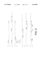
- FIG. 5 illustrates a timing diagram of signals used in accordance with the present invention.
- Signals 410, 415 and 440 are transistor-transistor level (TTL) logic signals.
- Signal 410 illustrates the vertical synchronization signal and each pulse 410a indicates the start of a new frame. Generally, frames are presented at 60 Hz. In non-interlaced refresh mode, pulse 410a indicates that the first row of FED 200 is ready to be energized.
- Signal train 415 represents the horizontal synchronization clock signal and pulses 415a-415c represent the start timing for energizing (e.g., refreshing) the first three exemplary row lines.
- Each pulse of 415a-415c indicates that a new row is to be energized (e.g., a new row of pixels are refreshed).
- pulses 415a, 415b and 415c correspond to the start of energizing of row one, row two and row three, respectively, of the rows of the FED flat panel display screen 200 (FIG. 3B).
- signal 440 represents the row enable signal generated by the one shot circuit 325 and transmitted over line 216 (FIG. 4) for the first three exemplary rows.
- Low asserted variable length pulses 440a-440c represent the on-time windows for all the row drivers 220a-220c.
- Variable length on-time widow pulses 440a-440c correspond, respectively, to the horizontal row synchronization clock pulses 415a-415c.
- each variable length on-time window 440a-440c only one row line of FED flat panel display screen 200 is active, as shown by the signals 420, 425 and 430.
- Signals 420, 425 and 430 correspond to the voltages seen over the three exemplary row lines.
- Driving voltage signal 420 corresponds to the first row
- driving voltage signal 425 corresponds to the second row
- driving voltage signal 430 corresponds to the third row.
- the dashed lines within signal 440 indicate that the on-time window is variable in pulse width depending on the current state of pulse width modulation circuit 300.
- signal 420 illustrates the voltage applied to an exemplary row line that is to be energized in synchronization with enable pulse 440a.
- Pulse 420a is the on-time window.
- the absolute maximum length of the on-time window can be the length of time between pulses of signal 415, e.g., from pulse 415a to pulse 415b, but can be arbitrarily set to a value less than this amount. In the example of FIG. 5, the maximum length of pulse 420a is arbitrarily set to about half of the period between pulses of signal 415 but could also occupy the entire period between horizontal synchronization pulses.
- This on-time window (pulse 420a) is variable as indicated by the different periods 2, 4, 6, 8, and 10 of FIG. 5. Brightness magnitude is linearly related to the length of the on-time window within the present invention. Therefore, period 10 (in this example) represents the full application of -Vcc to the exemplary row and corresponds to the maximum brightness of the FED flat panel display screen 200. Period 8 represents 6/7 of the full -Vcc application and represents an amount 6/7 of the full brightness. Period 6 represents 5/7 of the full -Vcc application and represents an amount 5/7 of the full brightness. Lastly, Period 2 represents 3/7 of the full -Vcc application and represents an amount 3/7 of the full brightness.
- periods 2-10 are selected per on-time pulse and that periods 2-10 of FIG. 5 are all shown as an example of the possible brightness levels of this embodiment of the present invention. It is appreciated further that in other examples, the maximum on-time window 420a can be increased to encompass the entire period between pulses of signal 415.
- a signal over line 312 (FIG. 4) is forwarded to circuit 300 such that pulse width of pulse 420a increases in size from a minimum pulse width 2.
- a signal over line 312 (FIG. 4) is forwarded to circuit 300 such that pulse width of pulse 420a decreased in size from a maximum of pulse width 10.
- the particular pulse width (e.g., of the on-time window) of pulses 420a, 425a and 430a depends on the value of the voltage controlled resistor 310 of FIG. 4 which is controlled by the brightness signal over line 312.
- FIG. 5 also illustrates signals 425 and 430 corresponding to two other exemplary row lines that are energized in synchronization with enable pulses 440b and 440c, respectively. Similar to pulse 420a, the pulse widths of pulses 425a and 430a are variable and depend on the pulse width of enable pulses 440b and 440c, respectively. For non-interlaced refresh mode, the row lines corresponding to pulses 420a, 425a and 430a are adjacent to each other on the FED flat panel display screen 200.
- the row on-time window can be synchronized to the horizontal synchronization clock signal 214 such that the end of the row on-time window coincides with the start of the pulses of the horizontal synchronization clock signal 214.
- the row on-time window is shortened or enlarged by altering the start point of the on-time window whereas FIG. 5 illustrates examples of altering the end point of the on-time window. It is appreciated that enlarging or shortening the row on-time window does not alter the power consumption characteristics of the FED screen 200 which are based significantly on the number of pulse transitions on the row lines. In accordance with the present invention, the number of pulse transitions on the row lines remains constant whether brightness is increased or decreased.
- circuit 250 of FIG. 4 is used, in conjunction with one shot circuit 325, to interrupt the voltage supplied over the voltage supply line 212 that feeds the row drivers 220a-220c.
- the TTL row enable signal 216 is coupled to a resistor 355 and used to control the gate of transistor 360.
- transistor 360 is coupled to a logic voltage level 305 and coupled to resistor 365 which is coupled in series to resistor 367 which is coupled to -Vcc or node 375.
- Voltage level -Vcc is the driving voltage level for the row lines of the FED flat panel display screen 200.
- the node between resistor 365 and resistor 367 is coupled to control the gate of transistor 370.
- Transistor 370 is coupled to node 375 (-Vcc) and also coupled to line 212. Therefore, in the second embodiment of the present invention, line 212 is not directly coupled to -Vcc 375.
- transistor 360 When the row enable line 216 is low, transistor 360 turns on causing a voltage at the gate of transistor 370 which turns on transistor 370. This causes line 212 to be coupled to -Vcc through transistor 370. Under this condition, -Vcc is supplied to all of the row drivers 220a-220c of the FED flat panel display screen 200. When the row enable line 216 is high, transistor 360 turns off causing transistor 370 to also turn off. This decouples line 212 from -Vcc. Under this condition, -Vcc is disconnected from the row drivers 220a-220c of the FED flat panel display screen 200.
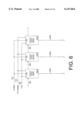
- FIG. 6 illustrates a third embodiment of the present invention for adjusting the brightness of an FED flat panel display screen 200.
- the on-time window of the column drivers 240a-240c are adjusted and a constant on-time window is used for the row drivers 220a-220c.
- FIG. 6 illustrates three exemplary column drivers 240a-240c of FED flat panel display screen 200 that drive exemplary columns 250f-250h, respectively. These three columns 250f-250h correspond to the red, green and blue lines of a column of pixels.
- Gray scale information is supplied over data bus 250 to the column drivers 240a-240c.
- the gray scale information causes the column drivers to assert different voltage amplitudes (amplitude modulation) to realize the different gray scale contents of the pixel. Different gray scale data for a row of pixels are presented to the column drivers 240a-240c for each pulse of the horizontal clock signal.
- Each column driver 240a-240c of FIG. 6 also has an enable input that is coupled to enable line 510 which is supplied in parallel to each column driver 240a-240c. Further, each column driver 240a-240c is also coupled to a column voltage line 515 which carries the maximum column voltage.
- the column drivers 240a-240c also receive a column clock signal for clocking in the gray scale data for a particular row of pixels.
- pulse width modulation is applied to the column drivers 240a-240c to implement brightness control. The longer the pulse width, the brighter the display in linear fashion. The shorter the pulse width, the darker the display.
- a column enable signal is generated by circuitry analogous to that shown in FIG. 4 and this column enable signal is coupled to column driver enable line 510.
- the column enable line 515 causes the on-time window for the column drivers 240a-240c to become variable, depending on the desired brightness of the FED flat panel display screen 200.
- the column drivers 240a-240c utilize voltage amplitude modulation to realize the gray scale content, but also use pulse width modulation to vary the brightness of the FED flat panel display screen 200.
- the third embodiment of the present invention does not degrade the gray scale resolution of the image.
- a fourth embodiment of the present invention is applicable for column drivers 240a-240c that do not have an enable input.
- a circuit is used analogous to circuit 350 of FIG. 4 to interrupt, e.g., turn on and off, the maximum column voltage supplied over line 515 in synchronization with the column on-time.
- a circuit analogous to circuit 350 is used to couple and decouple the maximum column voltage, Vcc, from line 515 and is controlled from an enable line analogous to enable line 216.
- the first and second embodiments of the present invention consume less power than the third and fourth embodiments because pulse width modulation of the column drivers 240a-240c requires driving against the capacitance of all the columns simultaneously whereas pulse width modulation of the row drivers 220a-220c only drives against the capacitance of a single row at a time. This is the case because during refresh, only one row is on at a time, but all columns are on so that an entire row of pixels are energized. It is further appreciated that performing brightness control using pulse width modulation, rather than using amplitude modulation, is advantageous because it does not degrade the gray scale resolution available to the FED flat panel display screen 200.
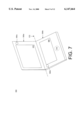
- FIG. 7 illustrates another embodiment of the present invention which includes an ambient light sensor 580 (FIG. 8) integrated within a general purpose computer system 550 having the FED flat panel display screen 200 therein.
- An exemplary portable computer system 550 in accordance with the present invention includes a keyboard or other alphanumeric data entry device 565.
- Computer system 550 also includes a cursor directing device 570 (e.g., a mouse, roller ball, finger pad, track pad, etc.) for directing a cursor across the FED flat panel display screen 200.
- the exemplary computer system 550 shown in FIG. 7 contains a base portion 590b and a retractable display portion 590a that optionally pivots about axis 572.
- the ambient light sensor 580 can be placed within a number of positions within the present invention and positions 580a and 580b are exemplary only. As described further below, for brightness normalization position 580b is advantageous and for automatic brightness adjustment position 580a is advantageous.
- Computer system 550 contains an address/data bus 500 for communicating address and data information, one or more central processors 501 coupled to the bus 500 for processing information and instructions.
- Computer system 550 includes a computer readable volatile memory unit 502 (e.g., random access memory, static RAM, dynamic, RAM, etc.) coupled with the bus 500 for storing information and instructions for the central processor(s) 501 and a computer readable non-volatile memory unit (e.g., read only memory, programmable ROM, flash memory, EPROM, EEPROM, etc.) 503 coupled with the bus 500 for storing static information and instructions for the processor(s) 501.
- a computer readable volatile memory unit 502 e.g., random access memory, static RAM, dynamic, RAM, etc.
- a computer readable non-volatile memory unit e.g., read only memory, programmable ROM, flash memory, EPROM, EEPROM, etc.
- the cursor control device 570 of FIG. 8 is coupled to the bus 500 for communicating user input information and command selections to the central processor(s) 501.
- Computer system 500 optionally includes a signal generating device 508 coupled to the bus 500 for communicating command selections to the processor(s) 501.
- Elements within 552 are generally internal to computer system 550.
- the present invention utilizes the ambient light sensor 580 in two embodiments.
- the brightness of the FED screen 200 is automatically increased.
- the brightness of the FED screen 200 is automatically decreased to maintain image viewing quality. This is done to maintain image viewing quality in a setting where the ambient light intensity is changing over time or if the display is transported to different settings having different ambient light intensities.
- the average brightness of the FED screen 200 is adjusted according to the circuitry described with respect to FIG. 4 herein.
- the manual adjustment knob 530 can be used as an override and allows the user to manually adjust the FED screen's brightness level.
- the sensor is used to provide brightness normalization for the FED screen 200 over the FED screen's useful lifetime.
- This embodiment is useful for brightness correcting of the FED screen 200 over age.
- the light sensor 580 is positioned such that it is exposed to a substantial amount of the FED screen's own light emission. As the light detected by the light sensor 580 falls below a predetermined threshold level, the average brightness of the FED screen 200 is increased. Likewise, as the light detected by the light sensor 580 rises above the predetermined threshold level, the average brightness of the FED screen 200 is decreased. Both of the above are performed in an attempt to bring the FED screen 200 to a factory preset brightness amount over the lifetime of the FED screen 200. In this embodiment, the average brightness of the FED screen 200 is adjusted according to the circuitry described with respect to FIG. 4 herein.
- FIG. 9 illustrates a block diagram of the first embodiment 600 of the present invention that utilizes the ambient light sensor 580 which is sensitive to ambient light 620.
- the light sensor 580 it is advantageous that the light sensor 580 not receive a substantial amount of light from the FED screen 200 itself since the light sensor 580 is to receive and respond to the ambient light in the surroundings of computer system 550.
- the sensor 580 can be placed in position 580a (FIG. 7) so that it is exposed to the ambient light but not substantially exposed to direct light from the FED screen 200.
- a number of different ambient light sensors 580 can be used in accordance with the present invention.
- One well known line of light sensors is commercially available from Texas Instruments and another is commercially available from Burr-Brown.
- Light sensors 580 used in accordance with the present invention generate a variable output signal in response to and in proportion to the light detected. Depending on the light sensor used, the output signal 585 can vary in current amount, voltage amount, oscillation frequency, and in pulse width with a fixed frequency.
- Another type of light sensor 580 is passive and varies in resistance as the light is varied.
- a comparison circuit 590 is used that receives a reference voltage signal 635 and also the output signal 585 of the sensor 580.
- the comparison circuit contains circuitry that generates the brightness voltage signal 312 in response to the values of signal 585 and 635.
- the comparison circuit converts the sensor output signal 585 (e.g., variable current, variable frequency, variable pulse width, or variable voltage, etc.) into a converted variable voltage signal that varies in proportion to the amount of light received by sensor 580.
- Well known circuits and components are used at this stage.
- switch 530 if switch 530 is "OFF” then the sensor output signal 585 and the converted variable voltage signal are ignored by the comparison circuit 590. In this case, comparison circuit 590 outputs the reference voltage signal 635 over line 312. However, if switch 530 is "ON,” then the converted variable voltage signal is then electrically added to the reference voltage level by the comparison circuit 590 to yield the brightness voltage signal the is output over line 312.
- the reference voltage signal 635 of FIG. 9 is generated by a reference circuit 630 that is coupled to the manual brightness adjustment knob 520.
- the manual brightness adjustment knob 520 controls a potentiometer element within circuit 630 that alters the reference voltage 635. As the manual adjustment knob 520 is adjusted to increase brightness, the reference voltage 635 is increased and as the manual adjustment knob 520 is adjusted to decrease brightness, the reference voltage 635 is decreased by circuit 630.
- the brightness voltage signal 312 controls circuit 300 of FIG. 9 as discussed above.
- circuit 300 can use pulse width modulation of the on-time window to control either the row drivers 220a-220c or the column drivers 240 to adjust the brightness of the FED flat panel display screen 200 as discussed in the embodiments above.
- the embodiment 600 of FIG. 9 performs as follows. If switch 530 is OFF and knob 520 is adjusted for more brightness, then brightness voltage signal 312 increases in amplitude causing the on-time window of circuit 300 to increase. If switch 530 is OFF and knob 520 is adjusted for less brightness, then brightness voltage signal 312 decreases in amplitude causing the on-time window of circuit 300 to decrease. If switch 530 is ON and manual adjust 520 is constant, then brightness voltage signal 312 automatically increases in voltage in direct proportion to any increase in detected ambient light from the light sensor 580. If switch 530 is ON and manual adjust 520 is constant, then brightness voltage signal 312 automatically decreases in voltage in direct proportion to any decrease in detected ambient light 620 from the ambient light sensor 580.
- the converted variable voltage of circuit 590 is added to the reference voltage signal 635, if switch 530 is ON and manual adjustment knob 520 is increased, the brightness voltage signal 312 increases assuming no change in ambient light 620. If switch 530 is ON and manual adjustment knob 520 is decreased, the brightness voltage signal 312 decreases assuming no change in ambient light 620. As discussed above, as the brightness signal 312 increases, the on-time window increases and the brightness of the FED screen 200 increases. Likewise, as the brightness signal 312 decreases, the on-time window decreases and the brightness of the FED screen 200 decreases.
- FIG. 10 illustrates a block diagram of the second embodiment 700 of the present invention that utilizes a light sensor 580 and this embodiment performs brightness normalization for FED screen 200.
- Brightness normalization samples the brightness of the FED screen 200 and alters the brightness of the FED screen 200 if the sampled amount varies from a predetermined preferred level.
- This embodiment 700 is used to maintain the average brightness of the FED screen 200 over its useful life and also to compensate for variations in manufacturing and variations in the FED screen 200 that occur over time.
- the light sensor 580 receive a substantial amount of light from the FED screen 200 itself as a reference source and not receive significant light from the ambient sources.
- the sensor 580 can be placed in position 580b (FIG. 7) so that it is exposed to direct light emitted from the FED screen 200 but not substantially exposed to the ambient light.
- a negative feedback loop 730 exists between the light sensor 380 and the light emitted from flat panel FED screen 200. Therefore, the brightness control circuitry 300 adjusts the brightness at flat panel screen 200 automatically in response to the light detected by sensor 380. Also, reference circuit 630' also adjusts the reference voltage over line 635 in response to the manual adjustment knob 520. In the mode of operation where both manual adjustment and automatic screen normalization are active at the same time, manual adjustment has override priority. In operation, as the light sensor 580 detects brighter light emitted from the FED screen 200 that exceeds a factory set threshold, circuit 300 causes the on-time pulse width to decrease, thereby causing the FED screen 200 to become less bright.
- Embodiment 700 also contains the full range of manual adjustment features as described with respect to embodiment 600. That is, increasing or decrease the reference voltage over line 635 also alters the brightness displayed on flat panel FED screen 200 in the manner described with reference to FIG. 9.
Abstract
Description
Claims (23)
Priority Applications (2)
| Application Number | Priority Date | Filing Date | Title |
|---|---|---|---|
| US09/164,402 US6147664A (en) | 1997-08-29 | 1998-09-30 | Controlling the brightness of an FED device using PWM on the row side and AM on the column side |
| PCT/US1999/014769 WO2000019399A1 (en) | 1998-09-30 | 1999-06-28 | Field emission display screen and method |
Applications Claiming Priority (2)
| Application Number | Priority Date | Filing Date | Title |
|---|---|---|---|
| US08/920,552 US6069597A (en) | 1997-08-29 | 1997-08-29 | Circuit and method for controlling the brightness of an FED device |
| US09/164,402 US6147664A (en) | 1997-08-29 | 1998-09-30 | Controlling the brightness of an FED device using PWM on the row side and AM on the column side |
Related Parent Applications (1)
| Application Number | Title | Priority Date | Filing Date |
|---|---|---|---|
| US08/920,552 Continuation-In-Part US6069597A (en) | 1997-08-29 | 1997-08-29 | Circuit and method for controlling the brightness of an FED device |
Publications (1)
| Publication Number | Publication Date |
|---|---|
| US6147664A true US6147664A (en) | 2000-11-14 |
Family
ID=22594325
Family Applications (1)
| Application Number | Title | Priority Date | Filing Date |
|---|---|---|---|
| US09/164,402 Expired - Lifetime US6147664A (en) | 1997-08-29 | 1998-09-30 | Controlling the brightness of an FED device using PWM on the row side and AM on the column side |
Country Status (2)
| Country | Link |
|---|---|
| US (1) | US6147664A (en) |
| WO (1) | WO2000019399A1 (en) |
Cited By (49)
| Publication number | Priority date | Publication date | Assignee | Title |
|---|---|---|---|---|
| US20020011978A1 (en) * | 2000-06-06 | 2002-01-31 | Semiconductor Energy Laboratory Co., Ltd. | Display device and method of manufacturing the same |
| US20020015110A1 (en) * | 2000-07-28 | 2002-02-07 | Clairvoyante Laboratories, Inc. | Arrangement of color pixels for full color imaging devices with simplified addressing |
| US6429836B1 (en) * | 1999-03-30 | 2002-08-06 | Candescent Intellectual Property Services, Inc. | Circuit and method for display of interlaced and non-interlaced video information on a flat panel display apparatus |
| US20020171778A1 (en) * | 2001-05-16 | 2002-11-21 | Hubby Laurence M. | Optical system for full color, video projector using single light valve with plural sub-pixel reflectors |
| US20020180750A1 (en) * | 2001-05-29 | 2002-12-05 | Imation Corp. | Display system |
| EP1274066A1 (en) * | 2001-07-03 | 2003-01-08 | Barco N.V. | Method and system for real time correction of an image |
| US20040046714A1 (en) * | 2001-05-09 | 2004-03-11 | Clairvoyante Laboratories, Inc. | Color flat panel display sub-pixel arrangements and layouts |
| US20040108976A1 (en) * | 2002-11-21 | 2004-06-10 | Hansen Ronald L. | System and method for adjusting field emission display illumination |
| US20050036162A1 (en) * | 2003-04-02 | 2005-02-17 | Edge Christopher J. | Ensuring accurate measurements for soft proofing system |
| US20050073516A1 (en) * | 2003-10-01 | 2005-04-07 | Mun-Seok Kang | Electron emission device and driving method thereof |
| US20050225562A1 (en) * | 2004-04-09 | 2005-10-13 | Clairvoyante, Inc. | Systems and methods for improved gamut mapping from one image data set to another |
| US20050250821A1 (en) * | 2004-04-16 | 2005-11-10 | Vincent Sewalt | Quaternary ammonium compounds in the treatment of water and as antimicrobial wash |
| US20050253835A1 (en) * | 2004-04-19 | 2005-11-17 | Sony Corporation | Active matrix type of display unit and method for driving the same |
| US20060097961A1 (en) * | 2004-11-10 | 2006-05-11 | Seonghak Moon | Plasma display apparatus and driving method thereof |
| US20060244686A1 (en) * | 2005-04-04 | 2006-11-02 | Clairvoyante, Inc | Systems And Methods For Implementing Improved Gamut Mapping Algorithms |
| US7167186B2 (en) | 2003-03-04 | 2007-01-23 | Clairvoyante, Inc | Systems and methods for motion adaptive filtering |
| US7187353B2 (en) | 2003-06-06 | 2007-03-06 | Clairvoyante, Inc | Dot inversion on novel display panel layouts with extra drivers |
| US20070071318A1 (en) * | 2003-09-11 | 2007-03-29 | Haruo Yamashita | Visual processing device, visual processing method, visual processing program, and semiconductor device |
| US7209105B2 (en) | 2003-06-06 | 2007-04-24 | Clairvoyante, Inc | System and method for compensating for visual effects upon panels having fixed pattern noise with reduced quantization error |
| US7218301B2 (en) | 2003-06-06 | 2007-05-15 | Clairvoyante, Inc | System and method of performing dot inversion with standard drivers and backplane on novel display panel layouts |
| US20070109447A1 (en) * | 2003-09-11 | 2007-05-17 | Haruo Yamashita | Visual processing device, visual processing method, visual processing program, and semiconductor device |
| US20070188623A1 (en) * | 2003-09-11 | 2007-08-16 | Haruo Yamashita | Visual processing device, visual processing method, visual processing program, intergrated circuit, display device, image-capturing device, and portable information terminal |
| US7268758B2 (en) | 2004-03-23 | 2007-09-11 | Clairvoyante, Inc | Transistor backplanes for liquid crystal displays comprising different sized subpixels |
| US7283142B2 (en) | 2000-07-28 | 2007-10-16 | Clairvoyante, Inc. | Color display having horizontal sub-pixel arrangements and layouts |
| US7301543B2 (en) | 2004-04-09 | 2007-11-27 | Clairvoyante, Inc. | Systems and methods for selecting a white point for image displays |
| US20080001787A1 (en) * | 2006-06-15 | 2008-01-03 | Apple Inc. | Dynamically controlled keyboard |
| US20080111500A1 (en) * | 2006-11-09 | 2008-05-15 | Apple Computer, Inc. | Brightness control of a status indicator light |
| US7397455B2 (en) | 2003-06-06 | 2008-07-08 | Samsung Electronics Co., Ltd. | Liquid crystal display backplane layouts and addressing for non-standard subpixel arrangements |
| US7403175B1 (en) | 2001-06-28 | 2008-07-22 | Canon Kabushiki Kaisha | Methods and systems for compensating row-to-row brightness variations of a field emission display |
| US20080211762A1 (en) * | 2007-03-02 | 2008-09-04 | Young Kim | Apparatus for adjusting luminance, display device having the same and method of adjusting luminance |
| US7590299B2 (en) | 2004-06-10 | 2009-09-15 | Samsung Electronics Co., Ltd. | Increasing gamma accuracy in quantized systems |
| US7592996B2 (en) | 2006-06-02 | 2009-09-22 | Samsung Electronics Co., Ltd. | Multiprimary color display with dynamic gamut mapping |
| US7598961B2 (en) | 2003-10-21 | 2009-10-06 | Samsung Electronics Co., Ltd. | method and apparatus for converting from a source color space to a target color space |
| US20100026705A1 (en) * | 2006-09-30 | 2010-02-04 | Moonhwan Im | Systems and methods for reducing desaturation of images rendered on high brightness displays |
| US7728802B2 (en) | 2000-07-28 | 2010-06-01 | Samsung Electronics Co., Ltd. | Arrangements of color pixels for full color imaging devices with simplified addressing |
| US20100149167A1 (en) * | 2008-12-17 | 2010-06-17 | Sony Corporation | Emissive type display device, semiconductor device, electronic device, and power supply line driving method |
| US7843559B2 (en) * | 2003-01-15 | 2010-11-30 | Applied Materials South East Asia Pte. Ltd. | System for detection of wafer defects |
| US20100328935A1 (en) * | 2009-06-30 | 2010-12-30 | Apple Inc. | Multicolor lighting system |
| US8031931B2 (en) | 2006-04-24 | 2011-10-04 | Applied Materials South East Asia Pte. Ltd. | Printed fourier filtering in optical inspection tools |
| US8035599B2 (en) | 2003-06-06 | 2011-10-11 | Samsung Electronics Co., Ltd. | Display panel having crossover connections effecting dot inversion |
| US8400626B2 (en) | 2010-06-10 | 2013-03-19 | Apple Inc. | Ambient light sensor |
| US8405692B2 (en) | 2001-12-14 | 2013-03-26 | Samsung Display Co., Ltd. | Color flat panel display arrangements and layouts with reduced blue luminance well visibility |
| US8436799B2 (en) | 2003-06-06 | 2013-05-07 | Samsung Display Co., Ltd. | Image degradation correction in novel liquid crystal displays with split blue subpixels |
| WO2014110553A1 (en) * | 2013-01-14 | 2014-07-17 | Apple Inc. | Low power display device with variable refresh rate |
| US20160148569A1 (en) * | 2014-11-26 | 2016-05-26 | Samsung Display Co., Ltd. | Organic light emitting display and method for driving the same |
| US20160155382A1 (en) * | 2014-11-27 | 2016-06-02 | Samsung Display Co., Ltd. | Display device and method of driving the display device |
| US10297191B2 (en) | 2016-01-29 | 2019-05-21 | Samsung Display Co., Ltd. | Dynamic net power control for OLED and local dimming LCD displays |
| CN113571027A (en) * | 2020-04-29 | 2021-10-29 | 北京小米移动软件有限公司 | Control method and device for display screen of electronic equipment, electronic equipment and storage medium |
| US11835382B2 (en) | 2021-03-02 | 2023-12-05 | Apple Inc. | Handheld electronic device |
Families Citing this family (2)
| Publication number | Priority date | Publication date | Assignee | Title |
|---|---|---|---|---|
| WO2002031803A1 (en) * | 2000-10-12 | 2002-04-18 | Candescent Technologies Corporation | Field emission display for interlaced and sequential video signals and related driving method |
| WO2004017292A1 (en) * | 2000-10-12 | 2004-02-26 | Candescent Technologies Corporation | Sequentially and interlacedly scanned field emission display |
Citations (32)
| Publication number | Priority date | Publication date | Assignee | Title |
|---|---|---|---|---|
| US3629653A (en) * | 1970-03-23 | 1971-12-21 | Us Of America The | Crossed grid el display driver technique |
| US3674928A (en) * | 1969-03-14 | 1972-07-04 | Matsushita Electric Ind Co Ltd | Scanning apparatus for electroluminescent crossed-grid panel |
| US3982063A (en) * | 1975-02-03 | 1976-09-21 | Bell Telephone Laboratories, Incorporated | Methods and apparatus for reducing the bandwidth of a video signal |
| US4130777A (en) * | 1977-02-16 | 1978-12-19 | Zenith Radio Corporation | Scanning means and method for a plasma-sac-type gas-discharge image display panel |
| US4170772A (en) * | 1978-04-26 | 1979-10-09 | The United States Of America As Represented By The Secretary Of The Army | Flat panel display with full color capability |
| US4694225A (en) * | 1985-09-30 | 1987-09-15 | Matsushita Electric Industrial Co., Ltd. | Method of driving a flat type of cathode ray tube to provide uniformity of electron beam emission characteristics for a plurality of beam sources |
| US4758828A (en) * | 1985-11-21 | 1988-07-19 | Alps Electric Co., Ltd. | Color thin-film EL display device |
| US5103145A (en) * | 1990-09-05 | 1992-04-07 | Raytheon Company | Luminance control for cathode-ray tube having field emission cathode |
| US5194780A (en) * | 1990-06-13 | 1993-03-16 | Commissariat A L'energie Atomique | Electron source with microtip emissive cathodes |
| US5262698A (en) * | 1991-10-31 | 1993-11-16 | Raytheon Company | Compensation for field emission display irregularities |
| US5357172A (en) * | 1992-04-07 | 1994-10-18 | Micron Technology, Inc. | Current-regulated field emission cathodes for use in a flat panel display in which low-voltage row and column address signals control a much higher pixel activation voltage |
| US5402143A (en) * | 1991-12-23 | 1995-03-28 | Panocorp Display Systems | Color fluorescent liquid crystal display |
| US5428370A (en) * | 1991-07-17 | 1995-06-27 | U.S. Philips Corporation | Matrix display device and its method of operation |
| US5459480A (en) * | 1992-04-07 | 1995-10-17 | Micron Display Technology, Inc. | Architecture for isolating display grid sections in a field emission display |
| US5477110A (en) * | 1994-06-30 | 1995-12-19 | Motorola | Method of controlling a field emission device |
| US5541473A (en) * | 1992-04-10 | 1996-07-30 | Silicon Video Corporation | Grid addressed field emission cathode |
| US5559389A (en) * | 1993-09-08 | 1996-09-24 | Silicon Video Corporation | Electron-emitting devices having variously constituted electron-emissive elements, including cones or pedestals |
| US5564959A (en) * | 1993-09-08 | 1996-10-15 | Silicon Video Corporation | Use of charged-particle tracks in fabricating gated electron-emitting devices |
| US5578899A (en) * | 1994-11-21 | 1996-11-26 | Silicon Video Corporation | Field emission device with internal structure for aligning phosphor pixels with corresponding field emitters |
| US5581159A (en) * | 1992-04-07 | 1996-12-03 | Micron Technology, Inc. | Back-to-back diode current regulator for field emission display |
| US5600345A (en) * | 1995-03-06 | 1997-02-04 | Thomson Consumer Electronics, S.A. | Amplifier with pixel voltage compensation for a display |
| US5607335A (en) * | 1994-06-29 | 1997-03-04 | Silicon Video Corporation | Fabrication of electron-emitting structures using charged-particle tracks and removal of emitter material |
| US5608283A (en) * | 1994-06-29 | 1997-03-04 | Candescent Technologies Corporation | Electron-emitting devices utilizing electron-emissive particles which typically contain carbon |
| US5625373A (en) * | 1994-07-14 | 1997-04-29 | Honeywell Inc. | Flat panel convergence circuit |
| US5659328A (en) * | 1993-12-22 | 1997-08-19 | Canon Kabushiki Kaisha | Electron beam generating apparatus, image display apparatus, and method of driving the apparatus |
| US5708451A (en) * | 1995-07-20 | 1998-01-13 | Sgs-Thomson Microelectronics, S.R.L. | Method and device for uniforming luminosity and reducing phosphor degradation of a field emission flat display |
| US5801671A (en) * | 1995-04-12 | 1998-09-01 | Sharp Kabushiki Kaisha | Liquid crystal driving device |
| US5856812A (en) * | 1993-05-11 | 1999-01-05 | Micron Display Technology, Inc. | Controlling pixel brightness in a field emission display using circuits for sampling and discharging |
| US5898415A (en) * | 1997-09-26 | 1999-04-27 | Candescent Technologies Corporation | Circuit and method for controlling the color balance of a flat panel display without reducing gray scale resolution |
| US5910792A (en) * | 1997-11-12 | 1999-06-08 | Candescent Technologies, Corp. | Method and apparatus for brightness control in a field emission display |
| US5949393A (en) * | 1996-03-11 | 1999-09-07 | Canon Kabushiki Kaisha | Image display apparatus having phosphors arranged in a checkerboard pattern and its driving method |
| US6034810A (en) * | 1997-04-18 | 2000-03-07 | Memsolutions, Inc. | Field emission charge controlled mirror (FEA-CCM) |
-
1998
- 1998-09-30 US US09/164,402 patent/US6147664A/en not_active Expired - Lifetime
-
1999
- 1999-06-28 WO PCT/US1999/014769 patent/WO2000019399A1/en active Application Filing
Patent Citations (32)
| Publication number | Priority date | Publication date | Assignee | Title |
|---|---|---|---|---|
| US3674928A (en) * | 1969-03-14 | 1972-07-04 | Matsushita Electric Ind Co Ltd | Scanning apparatus for electroluminescent crossed-grid panel |
| US3629653A (en) * | 1970-03-23 | 1971-12-21 | Us Of America The | Crossed grid el display driver technique |
| US3982063A (en) * | 1975-02-03 | 1976-09-21 | Bell Telephone Laboratories, Incorporated | Methods and apparatus for reducing the bandwidth of a video signal |
| US4130777A (en) * | 1977-02-16 | 1978-12-19 | Zenith Radio Corporation | Scanning means and method for a plasma-sac-type gas-discharge image display panel |
| US4170772A (en) * | 1978-04-26 | 1979-10-09 | The United States Of America As Represented By The Secretary Of The Army | Flat panel display with full color capability |
| US4694225A (en) * | 1985-09-30 | 1987-09-15 | Matsushita Electric Industrial Co., Ltd. | Method of driving a flat type of cathode ray tube to provide uniformity of electron beam emission characteristics for a plurality of beam sources |
| US4758828A (en) * | 1985-11-21 | 1988-07-19 | Alps Electric Co., Ltd. | Color thin-film EL display device |
| US5194780A (en) * | 1990-06-13 | 1993-03-16 | Commissariat A L'energie Atomique | Electron source with microtip emissive cathodes |
| US5103145A (en) * | 1990-09-05 | 1992-04-07 | Raytheon Company | Luminance control for cathode-ray tube having field emission cathode |
| US5428370A (en) * | 1991-07-17 | 1995-06-27 | U.S. Philips Corporation | Matrix display device and its method of operation |
| US5262698A (en) * | 1991-10-31 | 1993-11-16 | Raytheon Company | Compensation for field emission display irregularities |
| US5402143A (en) * | 1991-12-23 | 1995-03-28 | Panocorp Display Systems | Color fluorescent liquid crystal display |
| US5581159A (en) * | 1992-04-07 | 1996-12-03 | Micron Technology, Inc. | Back-to-back diode current regulator for field emission display |
| US5357172A (en) * | 1992-04-07 | 1994-10-18 | Micron Technology, Inc. | Current-regulated field emission cathodes for use in a flat panel display in which low-voltage row and column address signals control a much higher pixel activation voltage |
| US5459480A (en) * | 1992-04-07 | 1995-10-17 | Micron Display Technology, Inc. | Architecture for isolating display grid sections in a field emission display |
| US5541473A (en) * | 1992-04-10 | 1996-07-30 | Silicon Video Corporation | Grid addressed field emission cathode |
| US5856812A (en) * | 1993-05-11 | 1999-01-05 | Micron Display Technology, Inc. | Controlling pixel brightness in a field emission display using circuits for sampling and discharging |
| US5559389A (en) * | 1993-09-08 | 1996-09-24 | Silicon Video Corporation | Electron-emitting devices having variously constituted electron-emissive elements, including cones or pedestals |
| US5564959A (en) * | 1993-09-08 | 1996-10-15 | Silicon Video Corporation | Use of charged-particle tracks in fabricating gated electron-emitting devices |
| US5659328A (en) * | 1993-12-22 | 1997-08-19 | Canon Kabushiki Kaisha | Electron beam generating apparatus, image display apparatus, and method of driving the apparatus |
| US5607335A (en) * | 1994-06-29 | 1997-03-04 | Silicon Video Corporation | Fabrication of electron-emitting structures using charged-particle tracks and removal of emitter material |
| US5608283A (en) * | 1994-06-29 | 1997-03-04 | Candescent Technologies Corporation | Electron-emitting devices utilizing electron-emissive particles which typically contain carbon |
| US5477110A (en) * | 1994-06-30 | 1995-12-19 | Motorola | Method of controlling a field emission device |
| US5625373A (en) * | 1994-07-14 | 1997-04-29 | Honeywell Inc. | Flat panel convergence circuit |
| US5578899A (en) * | 1994-11-21 | 1996-11-26 | Silicon Video Corporation | Field emission device with internal structure for aligning phosphor pixels with corresponding field emitters |
| US5600345A (en) * | 1995-03-06 | 1997-02-04 | Thomson Consumer Electronics, S.A. | Amplifier with pixel voltage compensation for a display |
| US5801671A (en) * | 1995-04-12 | 1998-09-01 | Sharp Kabushiki Kaisha | Liquid crystal driving device |
| US5708451A (en) * | 1995-07-20 | 1998-01-13 | Sgs-Thomson Microelectronics, S.R.L. | Method and device for uniforming luminosity and reducing phosphor degradation of a field emission flat display |
| US5949393A (en) * | 1996-03-11 | 1999-09-07 | Canon Kabushiki Kaisha | Image display apparatus having phosphors arranged in a checkerboard pattern and its driving method |
| US6034810A (en) * | 1997-04-18 | 2000-03-07 | Memsolutions, Inc. | Field emission charge controlled mirror (FEA-CCM) |
| US5898415A (en) * | 1997-09-26 | 1999-04-27 | Candescent Technologies Corporation | Circuit and method for controlling the color balance of a flat panel display without reducing gray scale resolution |
| US5910792A (en) * | 1997-11-12 | 1999-06-08 | Candescent Technologies, Corp. | Method and apparatus for brightness control in a field emission display |
Cited By (101)
| Publication number | Priority date | Publication date | Assignee | Title |
|---|---|---|---|---|
| US6429836B1 (en) * | 1999-03-30 | 2002-08-06 | Candescent Intellectual Property Services, Inc. | Circuit and method for display of interlaced and non-interlaced video information on a flat panel display apparatus |
| US20020011978A1 (en) * | 2000-06-06 | 2002-01-31 | Semiconductor Energy Laboratory Co., Ltd. | Display device and method of manufacturing the same |
| US20020015110A1 (en) * | 2000-07-28 | 2002-02-07 | Clairvoyante Laboratories, Inc. | Arrangement of color pixels for full color imaging devices with simplified addressing |
| US6903754B2 (en) | 2000-07-28 | 2005-06-07 | Clairvoyante, Inc | Arrangement of color pixels for full color imaging devices with simplified addressing |
| US7274383B1 (en) * | 2000-07-28 | 2007-09-25 | Clairvoyante, Inc | Arrangement of color pixels for full color imaging devices with simplified addressing |
| US7728802B2 (en) | 2000-07-28 | 2010-06-01 | Samsung Electronics Co., Ltd. | Arrangements of color pixels for full color imaging devices with simplified addressing |
| US7283142B2 (en) | 2000-07-28 | 2007-10-16 | Clairvoyante, Inc. | Color display having horizontal sub-pixel arrangements and layouts |
| US7755648B2 (en) | 2001-05-09 | 2010-07-13 | Samsung Electronics Co., Ltd. | Color flat panel display sub-pixel arrangements and layouts |
| US20040046714A1 (en) * | 2001-05-09 | 2004-03-11 | Clairvoyante Laboratories, Inc. | Color flat panel display sub-pixel arrangements and layouts |
| US6950115B2 (en) | 2001-05-09 | 2005-09-27 | Clairvoyante, Inc. | Color flat panel display sub-pixel arrangements and layouts |
| US20050264588A1 (en) * | 2001-05-09 | 2005-12-01 | Clairvoyante, Inc | Color flat panel display sub-pixel arrangements and layouts |
| US20020171778A1 (en) * | 2001-05-16 | 2002-11-21 | Hubby Laurence M. | Optical system for full color, video projector using single light valve with plural sub-pixel reflectors |
| US7081928B2 (en) * | 2001-05-16 | 2006-07-25 | Hewlett-Packard Development Company, L.P. | Optical system for full color, video projector using single light valve with plural sub-pixel reflectors |
| US20020180750A1 (en) * | 2001-05-29 | 2002-12-05 | Imation Corp. | Display system |
| US7403175B1 (en) | 2001-06-28 | 2008-07-22 | Canon Kabushiki Kaisha | Methods and systems for compensating row-to-row brightness variations of a field emission display |
| EP2131345A2 (en) | 2001-06-28 | 2009-12-09 | Canon Kabushiki Kaisha | Method and system for measuring display attributes of a fed |
| CN1300760C (en) * | 2001-07-03 | 2007-02-14 | 巴科股份有限公司 | Method and system for image real time correction |
| EP1274066A1 (en) * | 2001-07-03 | 2003-01-08 | Barco N.V. | Method and system for real time correction of an image |
| US6950098B2 (en) | 2001-07-03 | 2005-09-27 | Barco N.V. | Method and system for real time correction of an image |
| US7038186B2 (en) * | 2001-07-03 | 2006-05-02 | Barco N.V. | Method and system for real time correction of an image |
| US20060151683A1 (en) * | 2001-07-03 | 2006-07-13 | Brabander Gino D | Method and system for real time correction of an image |
| US20050184983A1 (en) * | 2001-07-03 | 2005-08-25 | Brabander Gino D. | Method and system for real time correction of an image |
| US20030006980A1 (en) * | 2001-07-03 | 2003-01-09 | Brabander Gino De | Method and system for real time correction of an image |
| US7166829B2 (en) * | 2001-07-03 | 2007-01-23 | Gino De Brabander | Method and system for real time correction of an image |
| US8405692B2 (en) | 2001-12-14 | 2013-03-26 | Samsung Display Co., Ltd. | Color flat panel display arrangements and layouts with reduced blue luminance well visibility |
| US6771027B2 (en) * | 2002-11-21 | 2004-08-03 | Candescent Technologies Corporation | System and method for adjusting field emission display illumination |
| US20040108976A1 (en) * | 2002-11-21 | 2004-06-10 | Hansen Ronald L. | System and method for adjusting field emission display illumination |
| WO2004049288A1 (en) * | 2002-11-21 | 2004-06-10 | Canon Inc.(Canon Kabushiki Kaisha) | System, device, and method for pixel testing |
| US7843559B2 (en) * | 2003-01-15 | 2010-11-30 | Applied Materials South East Asia Pte. Ltd. | System for detection of wafer defects |
| US7167186B2 (en) | 2003-03-04 | 2007-01-23 | Clairvoyante, Inc | Systems and methods for motion adaptive filtering |
| US7864194B2 (en) | 2003-03-04 | 2011-01-04 | Samsung Electronics Co., Ltd. | Systems and methods for motion adaptive filtering |
| US20050036162A1 (en) * | 2003-04-02 | 2005-02-17 | Edge Christopher J. | Ensuring accurate measurements for soft proofing system |
| US8633886B2 (en) | 2003-06-06 | 2014-01-21 | Samsung Display Co., Ltd. | Display panel having crossover connections effecting dot inversion |
| US7397455B2 (en) | 2003-06-06 | 2008-07-08 | Samsung Electronics Co., Ltd. | Liquid crystal display backplane layouts and addressing for non-standard subpixel arrangements |
| US8436799B2 (en) | 2003-06-06 | 2013-05-07 | Samsung Display Co., Ltd. | Image degradation correction in novel liquid crystal displays with split blue subpixels |
| US9001167B2 (en) | 2003-06-06 | 2015-04-07 | Samsung Display Co., Ltd. | Display panel having crossover connections effecting dot inversion |
| US7218301B2 (en) | 2003-06-06 | 2007-05-15 | Clairvoyante, Inc | System and method of performing dot inversion with standard drivers and backplane on novel display panel layouts |
| US7187353B2 (en) | 2003-06-06 | 2007-03-06 | Clairvoyante, Inc | Dot inversion on novel display panel layouts with extra drivers |
| US8144094B2 (en) | 2003-06-06 | 2012-03-27 | Samsung Electronics Co., Ltd. | Liquid crystal display backplane layouts and addressing for non-standard subpixel arrangements |
| US8035599B2 (en) | 2003-06-06 | 2011-10-11 | Samsung Electronics Co., Ltd. | Display panel having crossover connections effecting dot inversion |
| US7573448B2 (en) | 2003-06-06 | 2009-08-11 | Samsung Electronics Co., Ltd. | Dot inversion on novel display panel layouts with extra drivers |
| US7209105B2 (en) | 2003-06-06 | 2007-04-24 | Clairvoyante, Inc | System and method for compensating for visual effects upon panels having fixed pattern noise with reduced quantization error |
| US7420577B2 (en) | 2003-06-06 | 2008-09-02 | Samsung Electronics Co., Ltd. | System and method for compensating for visual effects upon panels having fixed pattern noise with reduced quantization error |
| US7860339B2 (en) | 2003-09-11 | 2010-12-28 | Panasonic Corporation | Visual processing device, visual processing method, visual processing program, intergrated circuit, display device, image-capturing device, and portable information terminal |
| US7945115B2 (en) | 2003-09-11 | 2011-05-17 | Panasonic Corporation | Visual processing device, visual processing method, visual processing program, and semiconductor device |
| US20080107360A1 (en) * | 2003-09-11 | 2008-05-08 | Haruo Yamashita | Visual processing device, visual processing method, visual processing program, integrated circuit, display device, image-capturing device, and portable information terminal |
| US20070071318A1 (en) * | 2003-09-11 | 2007-03-29 | Haruo Yamashita | Visual processing device, visual processing method, visual processing program, and semiconductor device |
| US20100309216A1 (en) * | 2003-09-11 | 2010-12-09 | Haruo Yamashita | Visual processing device, visual processing method, visual processing program, and semiconductor device |
| US8165417B2 (en) | 2003-09-11 | 2012-04-24 | Panasonic Corporation | Visual processing device, visual processing method, visual processing program, integrated circuit, display device, image-capturing device, and portable information terminal |
| US20070188623A1 (en) * | 2003-09-11 | 2007-08-16 | Haruo Yamashita | Visual processing device, visual processing method, visual processing program, intergrated circuit, display device, image-capturing device, and portable information terminal |
| US7783126B2 (en) | 2003-09-11 | 2010-08-24 | Panasonic Corporation | Visual processing device, visual processing method, visual processing program, and semiconductor device |
| US20070109447A1 (en) * | 2003-09-11 | 2007-05-17 | Haruo Yamashita | Visual processing device, visual processing method, visual processing program, and semiconductor device |
| US20050073516A1 (en) * | 2003-10-01 | 2005-04-07 | Mun-Seok Kang | Electron emission device and driving method thereof |
| US7379079B2 (en) * | 2003-10-01 | 2008-05-27 | Samsung Sdi Co., Ltd. | Electron emission device and driving method thereof |
| US7598961B2 (en) | 2003-10-21 | 2009-10-06 | Samsung Electronics Co., Ltd. | method and apparatus for converting from a source color space to a target color space |
| US7268758B2 (en) | 2004-03-23 | 2007-09-11 | Clairvoyante, Inc | Transistor backplanes for liquid crystal displays comprising different sized subpixels |
| US7619637B2 (en) | 2004-04-09 | 2009-11-17 | Samsung Electronics Co., Ltd. | Systems and methods for improved gamut mapping from one image data set to another |
| US7864188B2 (en) | 2004-04-09 | 2011-01-04 | Samsung Electronics Co., Ltd. | Systems and methods for selecting a white point for image displays |
| US20050225562A1 (en) * | 2004-04-09 | 2005-10-13 | Clairvoyante, Inc. | Systems and methods for improved gamut mapping from one image data set to another |
| US7301543B2 (en) | 2004-04-09 | 2007-11-27 | Clairvoyante, Inc. | Systems and methods for selecting a white point for image displays |
| US20050250821A1 (en) * | 2004-04-16 | 2005-11-10 | Vincent Sewalt | Quaternary ammonium compounds in the treatment of water and as antimicrobial wash |
| US20050253835A1 (en) * | 2004-04-19 | 2005-11-17 | Sony Corporation | Active matrix type of display unit and method for driving the same |
| US7590299B2 (en) | 2004-06-10 | 2009-09-15 | Samsung Electronics Co., Ltd. | Increasing gamma accuracy in quantized systems |
| US7714806B2 (en) * | 2004-11-10 | 2010-05-11 | Lg Electronics Inc. | Plasma display apparatus and driving method thereof |
| US20060097961A1 (en) * | 2004-11-10 | 2006-05-11 | Seonghak Moon | Plasma display apparatus and driving method thereof |
| US8013867B2 (en) | 2005-04-04 | 2011-09-06 | Samsung Electronics Co., Ltd. | Systems and methods for implementing improved gamut mapping algorithms |
| US20060244686A1 (en) * | 2005-04-04 | 2006-11-02 | Clairvoyante, Inc | Systems And Methods For Implementing Improved Gamut Mapping Algorithms |
| US8031931B2 (en) | 2006-04-24 | 2011-10-04 | Applied Materials South East Asia Pte. Ltd. | Printed fourier filtering in optical inspection tools |
| US7592996B2 (en) | 2006-06-02 | 2009-09-22 | Samsung Electronics Co., Ltd. | Multiprimary color display with dynamic gamut mapping |
| US9086737B2 (en) | 2006-06-15 | 2015-07-21 | Apple Inc. | Dynamically controlled keyboard |
| US20080001787A1 (en) * | 2006-06-15 | 2008-01-03 | Apple Inc. | Dynamically controlled keyboard |
| US8259127B2 (en) | 2006-09-30 | 2012-09-04 | Samsung Electronics Co., Ltd. | Systems and methods for reducing desaturation of images rendered on high brightness displays |
| US20100026705A1 (en) * | 2006-09-30 | 2010-02-04 | Moonhwan Im | Systems and methods for reducing desaturation of images rendered on high brightness displays |
| US20100253228A1 (en) * | 2006-11-09 | 2010-10-07 | Apple Inc. | Brightness control of a status indicator light |
| US9144132B2 (en) | 2006-11-09 | 2015-09-22 | Apple Inc. | Brightness control of a status indicator light |
| US8653745B2 (en) | 2006-11-09 | 2014-02-18 | Apple Inc. | Brightness control of a status indicator light |
| US8610367B2 (en) | 2006-11-09 | 2013-12-17 | Apple Inc. | Brightness control of a status indicator light |
| US8373355B2 (en) * | 2006-11-09 | 2013-02-12 | Apple Inc. | Brightness control of a status indicator light |
| US20100253239A1 (en) * | 2006-11-09 | 2010-10-07 | Apple Inc. | Brightness control of a status indicator light |
| US20080111500A1 (en) * | 2006-11-09 | 2008-05-15 | Apple Computer, Inc. | Brightness control of a status indicator light |
| US8228321B2 (en) * | 2007-03-02 | 2012-07-24 | Samsung Electronics Co., Ltd. | Apparatus for adjusting luminance, display device having the same and method of adjusting luminance |
| US20080211762A1 (en) * | 2007-03-02 | 2008-09-04 | Young Kim | Apparatus for adjusting luminance, display device having the same and method of adjusting luminance |
| US20100149167A1 (en) * | 2008-12-17 | 2010-06-17 | Sony Corporation | Emissive type display device, semiconductor device, electronic device, and power supply line driving method |
| US8570314B2 (en) * | 2008-12-17 | 2013-10-29 | Sony Corporation | Emissive type display device, semiconductor device, electronic device, and power supply line driving method |
| US20100328935A1 (en) * | 2009-06-30 | 2010-12-30 | Apple Inc. | Multicolor lighting system |
| US8138687B2 (en) | 2009-06-30 | 2012-03-20 | Apple Inc. | Multicolor lighting system |
| US8400626B2 (en) | 2010-06-10 | 2013-03-19 | Apple Inc. | Ambient light sensor |
| WO2014110553A1 (en) * | 2013-01-14 | 2014-07-17 | Apple Inc. | Low power display device with variable refresh rate |
| CN105103214A (en) * | 2013-01-14 | 2015-11-25 | 苹果公司 | Low power display device with variable refresh rate |
| US9318069B2 (en) | 2013-01-14 | 2016-04-19 | Apple Inc. | Low power display device with variable refresh rates |
| US10600379B2 (en) | 2013-01-14 | 2020-03-24 | Apple Inc. | Low power display device with variable refresh rates |
| CN105103214B (en) * | 2013-01-14 | 2018-06-08 | 苹果公司 | Low-power with variable refresh rate shows equipment |
| US9501993B2 (en) | 2013-01-14 | 2016-11-22 | Apple Inc. | Low power display device with variable refresh rates |
| US10056050B2 (en) | 2013-01-14 | 2018-08-21 | Apple Inc. | Low power display device with variable refresh rates |
| US10170054B2 (en) * | 2014-11-26 | 2019-01-01 | Samsung Display Co., Ltd. | Organic light emitting display and method for driving the same |
| US20160148569A1 (en) * | 2014-11-26 | 2016-05-26 | Samsung Display Co., Ltd. | Organic light emitting display and method for driving the same |
| US9633601B2 (en) * | 2014-11-27 | 2017-04-25 | Samsung Display Co., Ltd. | Display device and method of driving the display device |
| US20160155382A1 (en) * | 2014-11-27 | 2016-06-02 | Samsung Display Co., Ltd. | Display device and method of driving the display device |
| US10297191B2 (en) | 2016-01-29 | 2019-05-21 | Samsung Display Co., Ltd. | Dynamic net power control for OLED and local dimming LCD displays |
| CN113571027A (en) * | 2020-04-29 | 2021-10-29 | 北京小米移动软件有限公司 | Control method and device for display screen of electronic equipment, electronic equipment and storage medium |
| US11835382B2 (en) | 2021-03-02 | 2023-12-05 | Apple Inc. | Handheld electronic device |
Also Published As
| Publication number | Publication date |
|---|---|
| WO2000019399A1 (en) | 2000-04-06 |
Similar Documents
| Publication | Publication Date | Title |
|---|---|---|
| US6147664A (en) | Controlling the brightness of an FED device using PWM on the row side and AM on the column side | |
| US6069597A (en) | Circuit and method for controlling the brightness of an FED device | |
| US6069598A (en) | Circuit and method for controlling the brightness of an FED device in response to a light sensor | |
| EP1402506B1 (en) | Method and system for row-by-row brightness correction in an FED | |
| US6204834B1 (en) | System and method for achieving uniform screen brightness within a matrix display | |
| US6429836B1 (en) | Circuit and method for display of interlaced and non-interlaced video information on a flat panel display apparatus | |
| US5898415A (en) | Circuit and method for controlling the color balance of a flat panel display without reducing gray scale resolution | |
| US6147665A (en) | Column driver output amplifier with low quiescent power consumption for field emission display devices | |
| JP4460776B2 (en) | Field emission display | |
| US20030058196A1 (en) | Method for reducing power consumption in field emission display devices by efficiently controlling column driver output voltage | |
| US6369783B1 (en) | Cell Driving apparatus of a field emission display | |
| KR20060104222A (en) | Driving device for electron emission display device and the method thereof | |
| JPH08226851A (en) | Plate voltage adjusting device for electric-field emitting device | |
| WO2002031803A1 (en) | Field emission display for interlaced and sequential video signals and related driving method | |
| WO2004017292A1 (en) | Sequentially and interlacedly scanned field emission display |
Legal Events
| Date | Code | Title | Description |
|---|---|---|---|
| AS | Assignment |
Owner name: CANDESCENT TECHNOLOGIES CORP., CALIFORNIA Free format text: ASSIGNMENT OF ASSIGNORS INTEREST;ASSIGNOR:HANSEN, RONALD L.;REEL/FRAME:009627/0239 Effective date: 19981124 |
|
| STCF | Information on status: patent grant |
Free format text: PATENTED CASE |
|
| AS | Assignment |
Owner name: CANDESCENT INTELLECTUAL PROPERTY SERVICES, INC., C Free format text: ASSIGNMENT OF ASSIGNORS INTEREST;ASSIGNOR:CANDESCENT TECHNOLOGIES CORPORATION;REEL/FRAME:011821/0569 Effective date: 20001205 |
|
| FEPP | Fee payment procedure |
Free format text: PAYOR NUMBER ASSIGNED (ORIGINAL EVENT CODE: ASPN); ENTITY STATUS OF PATENT OWNER: LARGE ENTITY |
|
| FPAY | Fee payment |
Year of fee payment: 4 |
|
| AS | Assignment |
Owner name: CANON KABUSHIKI KAISHA, JAPAN Free format text: NUNC PRO TUNC ASSIGNMENT EFFECTIVE AS OF AUGUST 26, 2004;ASSIGNOR:CANDESCENT TECHNOLOGIES CORPORATION;REEL/FRAME:019466/0437 Effective date: 20070104 |
|
| AS | Assignment |
Owner name: CANON KABUSHIKI KAISHA, JAPAN Free format text: NUNC PRO TUNC ASSIGNMENT;ASSIGNOR:CANDESCENT INTELLECTUAL PROPERTY SERVICES, INC.;REEL/FRAME:019580/0723 Effective date: 20061226 |
|
| AS | Assignment |
Owner name: CANDESCENT TECHNOLOGIES CORPORATION, CALIFORNIA Free format text: CORRECTIVE ASSIGNMENT TO CORRECT THE ASSIGNEE. THE NAME OF ONE ASSIGNEE WAS INADVERTENTLY OMITTED FROM THE RECORDATION FORM COVER SHEET PREVIOUSLY RECORDED ON REEL 011821 FRAME 0569;ASSIGNOR:CANDESCENT TECHNOLOGIES CORPORATION;REEL/FRAME:019679/0375 Effective date: 20001205 Owner name: CANDESCENT INTELLECTUAL PROPERTY SERVICES, INC., C Free format text: CORRECTIVE ASSIGNMENT TO CORRECT THE ASSIGNEE. THE NAME OF ONE ASSIGNEE WAS INADVERTENTLY OMITTED FROM THE RECORDATION FORM COVER SHEET PREVIOUSLY RECORDED ON REEL 011821 FRAME 0569;ASSIGNOR:CANDESCENT TECHNOLOGIES CORPORATION;REEL/FRAME:019679/0375 Effective date: 20001205 |
|
| FPAY | Fee payment |
Year of fee payment: 8 |
|
| FPAY | Fee payment |
Year of fee payment: 12 |