US6147740A - Liquid crystal panel and display including dichroic dye for absorbing yellow component of incident light - Google Patents
Liquid crystal panel and display including dichroic dye for absorbing yellow component of incident light Download PDFInfo
- Publication number
- US6147740A US6147740A US08/926,839 US92683997A US6147740A US 6147740 A US6147740 A US 6147740A US 92683997 A US92683997 A US 92683997A US 6147740 A US6147740 A US 6147740A
- Authority
- US
- United States
- Prior art keywords
- liquid crystal
- substrates
- pair
- crystal panel
- color compensation
- Prior art date
- Legal status (The legal status is an assumption and is not a legal conclusion. Google has not performed a legal analysis and makes no representation as to the accuracy of the status listed.)
- Expired - Lifetime
Links
Images


Classifications
-
- G—PHYSICS
- G02—OPTICS
- G02F—OPTICAL DEVICES OR ARRANGEMENTS FOR THE CONTROL OF LIGHT BY MODIFICATION OF THE OPTICAL PROPERTIES OF THE MEDIA OF THE ELEMENTS INVOLVED THEREIN; NON-LINEAR OPTICS; FREQUENCY-CHANGING OF LIGHT; OPTICAL LOGIC ELEMENTS; OPTICAL ANALOGUE/DIGITAL CONVERTERS
- G02F1/00—Devices or arrangements for the control of the intensity, colour, phase, polarisation or direction of light arriving from an independent light source, e.g. switching, gating or modulating; Non-linear optics
- G02F1/01—Devices or arrangements for the control of the intensity, colour, phase, polarisation or direction of light arriving from an independent light source, e.g. switching, gating or modulating; Non-linear optics for the control of the intensity, phase, polarisation or colour
- G02F1/13—Devices or arrangements for the control of the intensity, colour, phase, polarisation or direction of light arriving from an independent light source, e.g. switching, gating or modulating; Non-linear optics for the control of the intensity, phase, polarisation or colour based on liquid crystals, e.g. single liquid crystal display cells
- G02F1/137—Devices or arrangements for the control of the intensity, colour, phase, polarisation or direction of light arriving from an independent light source, e.g. switching, gating or modulating; Non-linear optics for the control of the intensity, phase, polarisation or colour based on liquid crystals, e.g. single liquid crystal display cells characterised by the electro-optical or magneto-optical effect, e.g. field-induced phase transition, orientation effect, guest-host interaction or dynamic scattering
- G02F1/13725—Devices or arrangements for the control of the intensity, colour, phase, polarisation or direction of light arriving from an independent light source, e.g. switching, gating or modulating; Non-linear optics for the control of the intensity, phase, polarisation or colour based on liquid crystals, e.g. single liquid crystal display cells characterised by the electro-optical or magneto-optical effect, e.g. field-induced phase transition, orientation effect, guest-host interaction or dynamic scattering based on guest-host interaction
-
- G—PHYSICS
- G02—OPTICS
- G02F—OPTICAL DEVICES OR ARRANGEMENTS FOR THE CONTROL OF LIGHT BY MODIFICATION OF THE OPTICAL PROPERTIES OF THE MEDIA OF THE ELEMENTS INVOLVED THEREIN; NON-LINEAR OPTICS; FREQUENCY-CHANGING OF LIGHT; OPTICAL LOGIC ELEMENTS; OPTICAL ANALOGUE/DIGITAL CONVERTERS
- G02F1/00—Devices or arrangements for the control of the intensity, colour, phase, polarisation or direction of light arriving from an independent light source, e.g. switching, gating or modulating; Non-linear optics
- G02F1/01—Devices or arrangements for the control of the intensity, colour, phase, polarisation or direction of light arriving from an independent light source, e.g. switching, gating or modulating; Non-linear optics for the control of the intensity, phase, polarisation or colour
- G02F1/13—Devices or arrangements for the control of the intensity, colour, phase, polarisation or direction of light arriving from an independent light source, e.g. switching, gating or modulating; Non-linear optics for the control of the intensity, phase, polarisation or colour based on liquid crystals, e.g. single liquid crystal display cells
- G02F1/133—Constructional arrangements; Operation of liquid crystal cells; Circuit arrangements
- G02F1/1333—Constructional arrangements; Manufacturing methods
- G02F1/1337—Surface-induced orientation of the liquid crystal molecules, e.g. by alignment layers
-
- G—PHYSICS
- G02—OPTICS
- G02F—OPTICAL DEVICES OR ARRANGEMENTS FOR THE CONTROL OF LIGHT BY MODIFICATION OF THE OPTICAL PROPERTIES OF THE MEDIA OF THE ELEMENTS INVOLVED THEREIN; NON-LINEAR OPTICS; FREQUENCY-CHANGING OF LIGHT; OPTICAL LOGIC ELEMENTS; OPTICAL ANALOGUE/DIGITAL CONVERTERS
- G02F1/00—Devices or arrangements for the control of the intensity, colour, phase, polarisation or direction of light arriving from an independent light source, e.g. switching, gating or modulating; Non-linear optics
- G02F1/01—Devices or arrangements for the control of the intensity, colour, phase, polarisation or direction of light arriving from an independent light source, e.g. switching, gating or modulating; Non-linear optics for the control of the intensity, phase, polarisation or colour
- G02F1/13—Devices or arrangements for the control of the intensity, colour, phase, polarisation or direction of light arriving from an independent light source, e.g. switching, gating or modulating; Non-linear optics for the control of the intensity, phase, polarisation or colour based on liquid crystals, e.g. single liquid crystal display cells
- G02F1/133—Constructional arrangements; Operation of liquid crystal cells; Circuit arrangements
- G02F1/1333—Constructional arrangements; Manufacturing methods
- G02F1/1335—Structural association of cells with optical devices, e.g. polarisers or reflectors
- G02F1/133509—Filters, e.g. light shielding masks
- G02F1/133514—Colour filters
-
- G—PHYSICS
- G02—OPTICS
- G02F—OPTICAL DEVICES OR ARRANGEMENTS FOR THE CONTROL OF LIGHT BY MODIFICATION OF THE OPTICAL PROPERTIES OF THE MEDIA OF THE ELEMENTS INVOLVED THEREIN; NON-LINEAR OPTICS; FREQUENCY-CHANGING OF LIGHT; OPTICAL LOGIC ELEMENTS; OPTICAL ANALOGUE/DIGITAL CONVERTERS
- G02F1/00—Devices or arrangements for the control of the intensity, colour, phase, polarisation or direction of light arriving from an independent light source, e.g. switching, gating or modulating; Non-linear optics
- G02F1/01—Devices or arrangements for the control of the intensity, colour, phase, polarisation or direction of light arriving from an independent light source, e.g. switching, gating or modulating; Non-linear optics for the control of the intensity, phase, polarisation or colour
- G02F1/13—Devices or arrangements for the control of the intensity, colour, phase, polarisation or direction of light arriving from an independent light source, e.g. switching, gating or modulating; Non-linear optics for the control of the intensity, phase, polarisation or colour based on liquid crystals, e.g. single liquid crystal display cells
- G02F1/137—Devices or arrangements for the control of the intensity, colour, phase, polarisation or direction of light arriving from an independent light source, e.g. switching, gating or modulating; Non-linear optics for the control of the intensity, phase, polarisation or colour based on liquid crystals, e.g. single liquid crystal display cells characterised by the electro-optical or magneto-optical effect, e.g. field-induced phase transition, orientation effect, guest-host interaction or dynamic scattering
- G02F1/13712—Devices or arrangements for the control of the intensity, colour, phase, polarisation or direction of light arriving from an independent light source, e.g. switching, gating or modulating; Non-linear optics for the control of the intensity, phase, polarisation or colour based on liquid crystals, e.g. single liquid crystal display cells characterised by the electro-optical or magneto-optical effect, e.g. field-induced phase transition, orientation effect, guest-host interaction or dynamic scattering the liquid crystal having negative dielectric anisotropy
-
- G—PHYSICS
- G02—OPTICS
- G02F—OPTICAL DEVICES OR ARRANGEMENTS FOR THE CONTROL OF LIGHT BY MODIFICATION OF THE OPTICAL PROPERTIES OF THE MEDIA OF THE ELEMENTS INVOLVED THEREIN; NON-LINEAR OPTICS; FREQUENCY-CHANGING OF LIGHT; OPTICAL LOGIC ELEMENTS; OPTICAL ANALOGUE/DIGITAL CONVERTERS
- G02F1/00—Devices or arrangements for the control of the intensity, colour, phase, polarisation or direction of light arriving from an independent light source, e.g. switching, gating or modulating; Non-linear optics
- G02F1/01—Devices or arrangements for the control of the intensity, colour, phase, polarisation or direction of light arriving from an independent light source, e.g. switching, gating or modulating; Non-linear optics for the control of the intensity, phase, polarisation or colour
- G02F1/13—Devices or arrangements for the control of the intensity, colour, phase, polarisation or direction of light arriving from an independent light source, e.g. switching, gating or modulating; Non-linear optics for the control of the intensity, phase, polarisation or colour based on liquid crystals, e.g. single liquid crystal display cells
- G02F1/137—Devices or arrangements for the control of the intensity, colour, phase, polarisation or direction of light arriving from an independent light source, e.g. switching, gating or modulating; Non-linear optics for the control of the intensity, phase, polarisation or colour based on liquid crystals, e.g. single liquid crystal display cells characterised by the electro-optical or magneto-optical effect, e.g. field-induced phase transition, orientation effect, guest-host interaction or dynamic scattering
- G02F1/139—Devices or arrangements for the control of the intensity, colour, phase, polarisation or direction of light arriving from an independent light source, e.g. switching, gating or modulating; Non-linear optics for the control of the intensity, phase, polarisation or colour based on liquid crystals, e.g. single liquid crystal display cells characterised by the electro-optical or magneto-optical effect, e.g. field-induced phase transition, orientation effect, guest-host interaction or dynamic scattering based on orientation effects in which the liquid crystal remains transparent
- G02F1/1393—Devices or arrangements for the control of the intensity, colour, phase, polarisation or direction of light arriving from an independent light source, e.g. switching, gating or modulating; Non-linear optics for the control of the intensity, phase, polarisation or colour based on liquid crystals, e.g. single liquid crystal display cells characterised by the electro-optical or magneto-optical effect, e.g. field-induced phase transition, orientation effect, guest-host interaction or dynamic scattering based on orientation effects in which the liquid crystal remains transparent the birefringence of the liquid crystal being electrically controlled, e.g. ECB-, DAP-, HAN-, PI-LC cells
-
- G—PHYSICS
- G02—OPTICS
- G02F—OPTICAL DEVICES OR ARRANGEMENTS FOR THE CONTROL OF LIGHT BY MODIFICATION OF THE OPTICAL PROPERTIES OF THE MEDIA OF THE ELEMENTS INVOLVED THEREIN; NON-LINEAR OPTICS; FREQUENCY-CHANGING OF LIGHT; OPTICAL LOGIC ELEMENTS; OPTICAL ANALOGUE/DIGITAL CONVERTERS
- G02F2202/00—Materials and properties
- G02F2202/04—Materials and properties dye
Definitions
- the present invention relates to a liquid crystal panel and a liquid crystal display using the panel.
- a liquid crystal panel and a liquid crystal display which is driven in a mode which aligns liquid crystal molecules having a negative dielectric anisotropy almost perpendicular to the substrates of the panel in the absence of applied voltage (vertical aligned mode, referred to as VA mode below).
- Liquid crystal displays are used widely as a display for various information processing devices, such as computers and TVs.
- a liquid crystal panel of a TN type, an STN type or a TFT type etc. is widely used in a mode which aligns the liquid crystal molecules having a positive dielectric anisotropy, i.e., a p type liquid crystal, parallel to the substrates opposed to each other in the absence of applied voltage.
- the alignment direction (the parallel direction) of the liquid crystal molecules adjacent to one substrate is usually twisted 90 degrees to that of the liquid crystal molecules adjacent to another substrate.
- a pair of polarizing plates disposed outside of the panel are arranged so that their transmission axes intersect at right angles with each other (crossed nicol)
- a white display is realized in a non-driving state
- a black display is realized in a driving state.
- the transmission axes of the polarizing plates are arranged parallel to each other (parallel nicol)
- a black display is realized in a non-driving state while a white display is realized in a driving state.
- liquid crystal molecules are aligned parallel to the substrate surface of the panel in a non-driving state, and on the contrary, they are aligned almost perpendicular to the substrate surface of the panel in a driving state.
- the liquid crystal molecules adjacent to the substrate surface of the panel keep the parallel alignment even in a driving state.
- the liquid crystal molecules in such a parallel alignment cause a birefringence which transmits some amount of light through the panel in a driving state. Due to this fact, a high contrast cannot be realized in the conventional TN mode liquid crystal panel.
- VA mode liquid crystal panels are being developed for practical application.
- a liquid crystal having a negative dielectric anisotropy is held between a pair of substrates forming the panel in a manner that the molecules of the liquid crystal are aligned almost perpendicular to the substrates.
- the VA mode liquid crystal panel has a problem that it is colored yellow when observed from an upper oblique direction. To avoid this problem, it is possible to decrease the retardation of a liquid crystal panel. However, the display contrast of the panel deteriorates as the retardation of the panel decreases, thus reducing the brightness of the panel.
- an objective of the present invention is to provide a liquid crystal panel and a liquid crystal display using the panel which shows a high contrast and no coloring in a white display.
- the first feature of the present invention provides a liquid crystal panel which is comprised of a pair of substrates, first and second electrodes formed on inner surfaces of the respective substrates, and first and second alignment films formed on the inner surfaces of the substrates to cover the first and the second electrodes respectively.
- a liquid crystal comprised of liquid crystal molecules having a negative dielectric anisotropy is provided between the two substrates to form a liquid crystal layer that contacts the first and the second alignment films.
- the liquid crystal layer contains a certain amount of dichroic dye, which is preferably a blue dichroic dye having a strong absorption band in yellow.
- the amount of this dye is 0.5 to 5 wt %, preferably, 1 to 3 wt % of the amount of liquid crystal layer.
- the dichroic dye is made of an anthraquinone dye.
- the dye may have a strong absorption coefficient in the direction parallel to the major axis of the dye molecules.
- the liquid crystal molecules in the panel are aligned almost perpendicular to the substrates in the absence of applied voltage because of their negative dielectric anisotropy.
- the molecules of the dichroic dye are aligned parallel to the liquid crystal molecules. Therefore, an excellent black display can be obtained in the absence of applied voltage when a pair of polarizing plates are disposed in crossed nicol.
- the liquid crystal molecules change their alignment direction so that a considerable angle, for example, about 45 degrees, is made against the substrate surfaces.
- the molecules of the blue dichroic dye change their alignment direction to keep a parallel alignment with the liquid crystal molecules. Therefore, an excellent white display is obtained when observing the panel from a direction perpendicular to the panel.
- a yellow coloring due to the alignment direction of the liquid crystal molecules is suppressed because of the yellow absorption characteristics of the blue dichroic dye since the molecules of this dye are aligned parallel to the alignment direction of the liquid crystal molecules.
- the yellow coloring was suppressed by increasing the value of retardation of the liquid crystal.
- the display contrast was deteriorated when the retardation became large.
- the present invention need not increase the retardation to suppress the yellow coloring, and a high contrast in the display can be maintained.
- a color compensation layer containing the dichroic dye is formed on at least one of the substrates, instead of adding the dichroic dye into the liquid crystal layer.
- the yellow coloring is suppressed by the color compensation layer containing the dichroic dye based on the same reason as the first feature. Therefore, a liquid crystal panel having a high contrast and substantially no yellow coloring can again be obtained.
- FIG. 1 is a schematic view showing the structure of a prior art liquid crystal panel of a VA mode
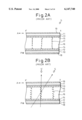
- FIG. 2A is a cross sectional view along line X-X' shown in FIG. 1 in the absence of applied voltage;
- FIG. 2B is a cross sectional view along line X-X' shown in FIG. 1 in the presence of applied voltage
- FIG. 3 is a graph showing the coloring characteristics of a prior art liquid crystal panel of a VA mode
- FIG. 4 is a graph showing the relation between the wavelength of an incident light and the transmittance thereof in various retardations of a liquid crystal
- FIG. 5 is a schematic view showing the structure of a VA mode liquid crystal panel according to the present invention.
- FIG. 6A is a cross sectional view along line Y-Y' shown in FIG. 5 in the absence of applied voltage, the view explaining the first principle of the present invention
- FIG. 6B is a cross sectional view along line Y-Y' shown in FIG. 5 in the presence of applied voltage, the view also explaining the first principle of the present invention
- FIG. 7 shows an example of the structural formula of a liquid crystal used in the present invention.
- FIG. 8 is a graph showing the absorption characteristics of a dichroic dye
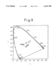
- FIG. 9 is a graph showing the coloring characteristics of a VA mode liquid crystal panel according to the present invention.
- FIG. 10 is a cross sectional view of the panel shown in FIG. 5 along line Y-Y', the view explaining the second principle of the present invention
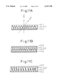
- FIGS. 11A to 11C are views for explaining the structures of a color compensation layer shown in FIG. 10;
- FIG. 12 is a schematic view showing the structure of a liquid crystal display of the present invention.
- FIG. 13 is a view showing the detailed structure of a part of the liquid crystal panel shown in FIG. 12;
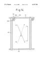
- FIG. 14 is a view showing an example of the structure of the liquid crystal panel shown in FIG. 13;
- FIG. 15A is a cross sectional view along line I-I' shown in FIG. 14 in the absence of applied voltage
- FIG. 15B is a cross sectional view along line I-I' shown in FIG. 14 in the presence of applied voltage
- FIG. 16 is a view showing another example structure of the liquid crystal panel shown in FIG. 13;
- FIG. 17A is a cross sectional view along line II-II' shown in FIG. 16 in the absence of applied voltage.
- FIG. 17B is a cross sectional view along line II-II' shown in FIG. 16 in the presence of applied voltage.
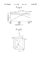
- FIG. 1 shows the structure of a prior art VA mode liquid crystal panel.
- light enters from the back surface of the paper and the panel is observed from the front surface of the paper.
- 1 and 2 denote a pair of substrates forming the liquid crystal panel and substrate 1 is on a light incident side and substrate 2 is on a light emitting side.
- An alignment film is coated on each of the inner surfaces of substrates 1 and 2, the inner surfaces being opposite to each other.
- Arrow Ri indicates an alignment direction of the alignment film formed on substrate 1 and arrow Ro indicates that of the film formed on substrate 2.
- Angle ⁇ 3 formed by the respective alignment directions of these films is 45 degrees.
- Arrow P indicates the direction of a transmission axis in a polarizing plate (not shown) disposed outside of substrate 1 on the light incident side
- arrow A indicates that of a polarizing plate (not shown) disposed outside of substrate 2 on the light emitting side.
- the transmission axes of these two polarizing plates intersect with each other at right angles.
- arrow S indicates a direction in which a yellow coloring is observed.
- FIGS. 2A and 2B show cross sections along line X-X' of the panel shown in FIG. 1, wherein FIG. 2A shows the panel in the absence of applied voltage (non-driving state) and FIG. 2B in the presence of an applied voltage (driving state).
- 10 denotes a first glass substrate forming a light incident side substrate, 11 a second glass substrate forming a light emitting side substrate, the first and the second glass substrates forming a pair of substrates.
- 12 denotes a first electrode formed on an inner surface of glass substrate 10, the inner surface being opposite to the second glass substrate 11, and 13 a second electrode formed on an inner surface of the second glass substrate 11, the inner surface facing the first glass substrate 10.
- the liquid crystal sandwiched by the first and second glass substrates 10 and 11 is driven by applying voltage to the electrodes 12 and 13 and forming an electric field therebetween.
- 14 denotes a first alignment film formed on substrate 10 to cover the first electrode 12
- 15 denotes a second alignment film formed on substrate 11 to cover second electrode 13.
- 16 denotes a liquid crystal layer comprised of liquid crystal molecules 17 having a negative dielectric anisotropy.
- 18 denotes a first polarizing plate, formed outside a first glass substrate 10, whose direction P of transmission is perpendicular to the paper surface, and 19 a second polarizing plate, formed outside second glass substrate 11, whose direction A of transmission is parallel to the paper surface.
- liquid crystal molecules 17 are aligned almost perpendicular to substrates 10 and 11 in the absence of voltage applied to first and second electrodes 12 and 13 as shown in FIG. 2A.
- An incident light (coming from the lower side of the figure) passing through the first polarizing plate 18 advances without its polarization plane changing, and therefore, it does not pass through the second polarizing plate 19 whose direction of the transmission axis is perpendicular to that of first polarizing plate 18.
- an excellent black display can be obtained.
- the excellent black display can also be obtained when observing the panel from an upper oblique direction (the direction shown by arrow S).
- a white display is obtained when observing the panel from a direction perpendicular to the panel (the direction shown by arrow S'), while it is colored yellow when observing the panel from an upper oblique direction (the direction shown by arrow S).
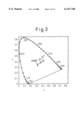
- FIG. 3 shows coloring characteristics of a prior art VA mode liquid crystal panel.
- observed color changes are plotted on a standard color system CIE (1931) while changing a visual angle from 90 degrees to 40 degrees.
- Symbol X in the figure indicates the standard white and numerals 450 to 625 indicate a wavelength (nm) of light. It can be seen from this figure that a blue light is observed around point 450, a green light is observed around point 525, and a red light is observed around point 625. It is also seen from this figure that an observed color point approaches towards a point 575 (nm) according to the change of the visual angle from 90 to 40 degrees. This means that the observed color changes towards yellow.
- FIG. 4 shows a relation between the wavelength of a light and the transmission thereof based on a various retardation ⁇ n ⁇ d of a liquid crystal, where ⁇ n means a refractive index anisotropy and d means a thickness of the liquid crystal layer.
- ⁇ n means a refractive index anisotropy
- d means a thickness of the liquid crystal layer.
- the axis of abscissa indicates a wavelength ⁇
- the longitudinal axis indicates a transmittance T of a light.
- This transmittance T is derived from the following equation:
- the respective curves in FIG. 4 represent the relations where ⁇ n ⁇ d is 200 nm, 275 nm and 350 nm respectively. As easily understood from FIG. 4, peaks of the respective curves move to the longer wavelength side as ⁇ n ⁇ d increases.
- liquid crystal molecules 17 are aligned almost parallel to the light passing through liquid crystal layer 16 perpendicularly.
- the parallel axis of the liquid crystal molecules are almost parallel to the light advancing direction.
- the effective value of ⁇ n ⁇ d for a light advancing perpendicular to the panel surface becomes 220 nm, thus allowing an excellent black display.
- liquid crystal molecules 17 have a tilt angle of 45 degrees to the light advancing through the liquid crystal layer 16 perpendicularly.
- the refractive index anisotropy ⁇ n of the liquid crystal varies according to the incident angle of the light into the layer.
- an effective thickness d of the liquid crystal layer varies according to the incident angle of the light into this layer. Taking account of those points, the effective value of ⁇ n ⁇ d along direction S' shown in FIG. 2B becomes 275 nm, and thus, an excellent white display is obtained, as shown in FIG. 4, and the incident light passes through the liquid crystal layer uniformly over the entire (visible) wavelength range.
- the major axis direction of liquid crystal molecules 17 forms an angle of about 90 degrees with the observing direction.
- ⁇ n has a larger value than when the angle is about 45 degrees.
- the effective thickness d becomes longer since the effective distance the light passes through the layer becomes longer, resulting in an effective value ⁇ n ⁇ d of about 400 nm.
- the prior art VA mode liquid crystal panel has a problem that, when looking into the panel from an upper oblique direction, a yellow display occurs if light passing though a liquid crystal layer produces a large angle (for example, about 90 degrees) against the alignment direction of the liquid crystal molecules.
- the yellow display may be observed when a voltage is applied even though the panel is observed in the presence of an applied voltage even when observing the panel from a perpendicular direction.
- the value ⁇ n ⁇ d small when forming the panel.
- the display becomes dark even though the panel is observed from a perpendicular direction, thus reducing the brightness of the panel. Accordingly, high contrast, which is considered as an important advantage of the VA mode liquid crystal panel, is lost.
- the panel when the value ⁇ n ⁇ d is selected large enough to obtain a high contrast, the panel will be seen as yellow depending on the visual angle. Contrary to this, the contrast of the display becomes low when ⁇ n ⁇ d is set to a small value to avoid the coloring of the display which depends on the visual angle.
- FIG. 5 shows the structure of a VA mode liquid crystal panel according to the present invention.
- FIG. 5 it is assumed that light enters the panel from the back surface of the paper and the panel is observed from the front surface of the paper.
- 21 and 22 denote a pair of substrates forming the liquid crystal panel and substrate 21 is placed on the light incident side whilst substrate 22 is on the light emitting side.
- An alignment film is coated on each of inner surfaces of substrates 21 and 22, the inner surfaces facing each other.
- Arrow Ri indicates the alignment direction of the alignment film formed on substrate 21 and arrow Ro indicates that of the film formed on substrate 22.
- Angle ⁇ 0 formed by the alignment directions of these films is 45 degrees.
- Arrow P indicates the direction of the transmission axis of a polarizing plate (not shown) disposed outside substrate 21 on the light incident side
- arrow A indicates that of another polarizing plate (not shown) disposed outside substrate 22 on the light emitting side.
- the transmission axes of these two polarizing plates intersect with each other at right angles.
- arrow S indicates a direction in which a yellow coloring appears, that is, a visual angle in an upper oblique direction.
- FIGS. 6A and 6B show the cross sections along line Y-Y' indicated in FIG. 5, for explaining the first principle of the present invention.
- FIG. 6A shows the cross section of the panel in the absence of applied voltage (non-driving state) whilst FIG. 6B shows that of the panel in the presence of applied voltage (driving state).
- 20 denotes a first glass substrate forming a substrate of the panel on the light incident side, 21 a second glass substrate forming another substrate on the light emitting side, the first and the second glass substrates forming the pair of substrates disposed parallel to each other.
- 22 denotes a first electrode formed on an inner surface of glass substrate 20, the inner surface facing the second glass substrate 21, and 23 a second electrode formed on an inner surface of second glass substrate 21, the inner surface facing the first glass substrate 20.
- the liquid crystal sandwiched by first and second glass substrates 20 and 21 are driven by applying a voltage to these electrodes 22 and 23 and forming an electric field therebetween.
- 24 denotes a first alignment film formed on plate 20 to cover first electrode 22, and 25 a second alignment film formed on plate 21 to cover second electrode 23. These two alignment films cause liquid crystal molecules to be aligned vertical to the glass substrates.
- 26 denotes a liquid crystal layer comprised of liquid crystal molecules 27 having a negative dielectric anisotropy.
- 29 denotes a first polarizing plate disposed outside first glass substrate 20, the polarizing plate whose direction P of the transmission axis is perpendicular to the paper surface, and 30 a second polarizing plate, disposed outside second glass substrate 21, whose direction A of the transmission axis is parallel to the paper surface.
- the present invention is characterized in that a blue dichroic dye 28 is further added to liquid crystal layer 26.
- the molecules of dye 28 have an elongated shape similar to that of the liquid crystal molecules and have a strong absorption direction along the major axis of the molecules.
- the molecules of dye 28 are aligned in parallel with the liquid crystal molecules, and absorb a yellow color component contained in the incident light.
- Dye 28 has a characteristic feature that the absorption coefficient of dye 28 in the yellow color band becomes larger as the polarization direction of an incident light approaches parallel to the major axis direction of the dye molecules.
- liquid crystal molecules 27 are aligned almost perpendicular to glass substrates 20 and 21 (as shown in FIG. 6A) in the absence of applied voltage across electrodes 22 and 23.
- incident light which has passed the first polarizing plate 29 (the light coming from the lower side of plate 20 as shown in FIG. 6B), advances through liquid crystal layer 26 without changing its polarization direction.
- the light cannot pass the second polarizing plate 30 whose polarization direction is perpendicular to that of first polarizing plate 29, thus allowing an excellent black display.
- an excellent black display is also obtained when observing the panel from the upper oblique direction S.
- the liquid crystal panel according to the present invention presents a desired white display when observing the panel from the panel front (the direction indicated by arrow S').
- the yellow coloring of the panel is suppressed and an excellent white display can also be obtained when observing the panel from the upper oblique direction S.
- the molecules of dye 28 tend to be aligned parallel to liquid crystal molecules 27, and as a result, they make an angle of about 90 degrees with the incident light to strongly absorb a yellow color component in the incident light while it advances through the liquid crystal layer.
- FIG. 6 An evaluation has been made for the structure shown in FIG. 6 to test the effect of the present invention.
- Boron silicate glass having a thickness of 1.1 mm is used as a material of glass substrates 20 and 21 and vertical alignment film RN722 having a thickness of 800 ⁇ made by Nissan Kagaku Ltd. is used as the material of alignment films 24 and 25.
- a chiral agent (CN made by Chisso Ltd.) is added to 1 wt % into liquid crystal layer 26 and the thickness of the layer is set to 4 ⁇ m.
- An anthraquinone dye (SI-497 made by Mitsui-Toatsu Ltd.) is added to 1 wt % as a dichroic dye.
- FIG. 8 shows the absorption characteristics of this dichroic dye wherein the vertical axis indicates an absorption coefficient and the axis of abscissa indicates an absorption wavelength.
- the dichroic dye used in this evaluation has an absorption peak around 650 nm so that it absorbs yellow light efficiently.
- FIG. 9 shows the coloring characteristic of the VA mode liquid crystal panel according to the present invention.
- color changes are plotted on the standard CIE (1931) color system by varying the visual angle from 0 (the panel front) to 40 degrees (the upper oblique direction).
- Symbol X in this figure shows the standard white.
- a monochromatic liquid crystal cell was used which has the above mentioned structure.
- the yellow coloring is reduced even if the visual angle declines to the upper oblique direction, i.e., an angle of 40 degrees. This phenomenon is more apparent when compared with the coloring characteristics of the conventional liquid crystal panel shown in FIG. 3, the evaluation of the characteristics being carried out in the same structure as that of the panel shown in FIGS. 5 and 6 except that no dye is added into the liquid crystal layer.
- the effective retardation value from which the yellow coloring becomes remarkable even though a dye is added into the liquid crystal layer is larger than 350 nm which is a value obtained by applying no dichroic dye into the liquid crystal layer. It should be noted, however, that this value changes depending on materials of the dye and the added amount of the dye.
- FIG. 10 is a view for explaining the second principle of the present invention.
- FIG. 10 is a cross sectional view along line Y-Y' shown in FIG. 5 in the presence of applied voltage (in a driving condition).
- 31 denotes a first glass substrate forming a substrate on the light incident side and 32 a second glass substrate forming another substrate on the light emitting side, these two glass substrates forming a pair of substrates.
- 33 denotes a first electrode formed on an inner surface of glass substrate 31, the inner surface facing the second glass substrate 32, and 34 a second electrode formed on an inner surface of glass substrate 32, the inner surface facing the first glass substrate 31.
- An electric field is generated by applying a voltage across these electrodes.
- 35 denotes a first alignment film formed on glass substrate 31 to cover first electrode 33, and 36 a second alignment film formed on glass substrate 32 to cover second electrode 34.
- 37 denotes a liquid crystal layer comprised of a plurality of liquid crystal molecules 38 having a negative dielectric anisotropy.
- 39 denotes a first polarizing plate disposed outside first glass substrate 31 and having transmission axis P vertical to the paper surface, and 40 a second polarizing plate disposed outside glass substrate 32 and having transmission axis A parallel to the paper surface. Therefore, the transmission axes of these two polarizing plates intersect with each other at right angles.
- a color compensation layer 41 denotes a color compensation layer containing a blue dichroic dye, this layer forming a characteristic feature of the present invention.
- a color compensation layer 41 is disposed between second glass substrate 32 and second polarizing plate 40. The yellow coloring, which appeared when the visual angle is in an upper oblique direction, is compensated for by the color compensating layer 41, thus providing an excellent display.
- FIGS. 11A to 11C show various structures of the color compensation layer.
- the color compensation layer 41 shown in FIG. 11A is comprised of a support 41a made from a PET (polyethylene terephthalate) film, liquid crystal polymer 41b hardened by ultra-violet radiation and a blue dichroic dye 41c aligned perpendicular to support 41a in liquid crystal polymer 41b.
- the color compensation layer 41' shown in FIG. 11B has a structure to sandwich the liquid crystal polymer 41b by a surface layer 41d made from a PET film and the support 41a.
- the blue dichroic dye 41c has the same characteristics as that of dye 28 shown in FIG. 2.
- the color compensation layer 41" shown in FIG. 11C has the same structure as that of shown in FIG. 11B except that the molecules of the blue dichroic dye 41c are aligned obliquely to the support 41a.
- liquid crystal molecules 38 are aligned almost perpendicular to the substrates in the absence of applied voltage across electrodes 33 and 34.
- liquid crystal molecules change their alignment direction according to the applied voltage, thus forming an angle of 45 degrees to substrates 31 and 32.
- the liquid crystal panel of the present invention gives a desirable white display when observing the panel from the panel front (the direction shown by arrow S').
- the panel appears to be slightly colored blue when observed from the panel front (the direction indicated by arrow S').
- the yellow coloring of the panel is suppressed better than the case of the panel using the color compensation layer 41 or 41'.
- FIG. 12 shows a structure of a liquid crystal display of the present invention.
- 50 denotes a liquid crystal display comprising a liquid crystal panel 51 according to the present invention and first and second driving circuits 52 and 53.
- liquid crystal panel 51 is an active-matrix type liquid crystal panel
- first driving circuit 52 provides display data to panel 51
- second driving circuit 53 provides scan data to panel 51.
- FIG. 13 is a view for explaining the detailed structure of liquid crystal panel 51 shown in FIG. 12.
- a TFT substrate is shown which forms an active-matrix type liquid crystal panel using a plurality of thin film transistors (referred to as TFT, below) as switching elements.
- FIG. 13 54 denotes a glass substrate, 55 a plurality of gate bus lines arranged parallel to each other, 56 a plurality of drain bus lines arranged parallel to each other, 57 a plurality of TFTs, and 58 a plurality of pixel electrodes.
- Each gate bus line and each drain bus line are electrically insulated and intersect with each other at right angles to form a matrix.
- a TFT 57 and a pixel electrode 58 are formed on each intersecting portion of gate bus line 55 and drain bus line 56.
- the gate electrode of TFT 57 is connected with gate bus line 55 and the drain electrode is connected with drain bus line 56 respectively.
- the source electrode of TFT 57 is connected with pixel electrode 58.
- a common substrate is arranged oppositely to the TFT substrate and a liquid crystal layer is sealed between the two substrates.
- a common electrode, a color filter and so on are formed on the common substrate.
- FIGS. 14 to 17 show a various examples of one pixel of the liquid crystal panel according to the present invention, wherein FIGS. 14 and 15 show a first example and FIGS. 16 and 17 show a second example.
- FIGS. 14 and 15 show a pixel portion of the liquid crystal panel according to the present invention, wherein FIG. 15 is a cross sectional view of the pixel taken along line I-I' shown in FIG. 14.
- 61 denotes a gate bus line and 62 a drain bus line, wherein these lines are insulated by means of an insulating film from each other at their intersecting portion.
- 63 denotes a TFT formed at an intersection of gate bus line 61 and drain bus line 62.
- 64 denotes a pixel electrode.
- TFT 63 is comprised of a gate electrode 63a, drain electrode 63b, and a source electrode 63c.
- Gate electrode 63a is formed as a part of gate bus line 61 and drain electrode 63b is formed as a part of drain bus line 62.
- a source electrode 63c is electrically connected with a pixel electrode 64.
- Ri indicates a rubbing direction of the alignment film formed on the TFT substrate
- Ro indicates another rubbing direction of another alignment film formed on the common substrate (shown in FIGS. 15A and 15B) facing the TFT substrate.
- the angle ⁇ 1 formed between the respective rubbing directions Ri and Ro is about 45 degrees.
- FIG. 15A shows the cross section along the line I-I' shown in FIG. 14 in the absence of voltage (non-driving condition) and FIG. 15B shows that of in the presence of voltage (driving condition).
- FIGS. 15A and 15B 78 denotes the TFT substrate and 79 the common substrate mentioned above.
- TFT substrate 78 is comprised of a first glass substrate 65, an insulating film 67 formed on a surface of first glass substrate 65 which surface faces a common substrate 79, a pixel electrode 64 formed on insulating film 67, a first vertical alignment film 68 formed to cover pixel electrode 64, and a polarizing plate 69 disposed outside first glass substrate 65 and having a transmission axis whose direction is perpendicular to the paper surface.
- Common substrate 79 is comprised of a second glass substrate 66, a color filter layer 70 formed on a surface of second glass substrate 66 which surface faces to TFT substrate 78, a protection film 71 for covering and protecting color filter 70, a common electrode 72 formed on protection film 71, a second vertical alignment film 73 formed to cover common electrode 72, and a polarizing plate 74 disposed outside second glass substrate 66 and having a transmission axis A parallel to the paper surface.
- Liquid crystal layer 75 denotes a liquid crystal layer sandwiched by TFT substrate 78 and a common substrate 79.
- Liquid crystal layer 75 is comprised of liquid crystal molecules 76 having a negative dielectric anisotropy containing a blue dichroic dye 77.
- liquid crystal molecules 76 ones adjacent to TFT substrate 78 and common substrate 79 have a pre-tilt angle of 89 degrees.
- the pre-tilt angle is set to more than or equal to 75 degrees and less than 90 degrees, and more preferable, more than or equal to 87 degrees.
- both the liquid crystal molecules 76 and the dye molecule 77 align almost perpendicular to substrates 78 and 79 in the absence of an applied voltage. Since the polarization axes of two polarizing plates 69 and 74 are disposed to intersect each other at right angles, an excellent black display can be obtained in this case.
- liquid crystal molecules 76 change the alignment direction towards a direction parallel to substrates 78 and 79 in the presence of applied voltage.
- dye 77 changes the alignment direction towards a direction parallel to substrates 78 and 79 since molecules of dye 77 tend to align parallel to liquid crystal molecules 76.
- FIGS. 16 and 17 show the second example of a pixel portion of the liquid crystal panel, which is of an active matrix type, according to the present invention.
- FIG. 17A is a cross sectional view along line II-II' shown in FIG. 16 in the absence of applied voltage and
- FIG. 17B is the same view as that of shown in FIG. 17A in the presence of applied voltage.
- the same numerals as those shown in FIG. 14 denote the same or similar structure elements.
- the pixel shown in FIG. 16 differs from that shown in FIG. 14 in the rubbing structures of the alignment films provided on the TFT substrate and the common substrate.
- one pixel is divided into two regions (i) and (ii) whose alignment directions differ from each other.
- This structure is called an alignment division.
- various methods are known to accomplish the alignment division, the present example forms the two regions by changing the rubbing directions of these regions.
- the pixel region is divided into a first region (i) and a second region (ii), each region being rubbed in direction Ria or Rib opposite to each other.
- the pixel region is divided into a first (i) and a second region (ii) corresponding to the first and second regions formed on the alignment film of the TFT substrate.
- the first and the second regions on the common substrates are rubbed in direction Roa or Rob opposite to each other.
- angle ⁇ 2a between rubbing directions Ria and Roa in first region (i) and angle ⁇ 2b between rubbing directions Rib and Rob in second region (ii) are 45 degrees respectively.
- FIG. 17A shows a cross section along line II-II' of the liquid crystal panel shown in FIG. 16 in the absence of an applied voltage (non-driving state) and FIG. 17B shows that of in the presence of an applied voltage (driving state).
- TFT substrate 86 has two regions 81a and 81b in alignment film 81, each region having a different rubbing direction corresponding to first region (i) or second region (ii).
- common substrate 87 has two regions 82a and 82b in alignment film 82, each region having a different rubbing direction to each other corresponding to first region (i) or second region (ii), a color compensation layer 85 is disposed between glass substrate 66 and polarizing plate 74, and liquid crystal layer 83 only consists of liquid crystal molecules 84.
- the color compensation layers shown in FIG. 11 can be used as color compensation layer 85 shown in FIG. 17.
- the layer is formed as a structural element in which blue dichroic dye is arranged vertically or obliquely in a predetermined angle.
- any one of color compensation layers 41, 41' or 41" shown in FIGS. 11A, 11B and 11C can be used to be color compensation layer 85 shown in FIG. 17.
- 41a indicates the PET film
- 41b the liquid crystal polymer hardened by irradiation of an ultra-violet light
- 41c the blue dichroic dye.
- the surface of PET film 41a is pre-treated so that the liquid crystal molecules are aligned perpendicular to the surface.
- Such a pre-treatment includes applying on PET film 41a a film having a property to align liquid crystal molecules perpendicular to the film surface.
- a film includes a vertical alignment film widely used for forming a liquid crystal panel, a film of a silane coupling agent, and a film of a monobasic carboxylic acid chromium complex.
- each liquid crystal molecule of high molecular liquid crystal 41b is aligned almost perpendicular to film 41a. Accordingly, the molecules of blue dichroic dye 41c are also aligned almost perpendicular to PET film 41a. In this situation, then, an ultra-violet light is applied to polymerize and harden a high molecule liquid crystal 41b. As a result, color compensation layer 85 (41) is formed to include blue dichroic dye 41c which are aligned almost perpendicular to the layer.
- Color compensation layer 41' shown in FIG. 11B has a structure in which a PET film 41d is formed to cover the structure shown in FIG. 11A. Layer 41' can be formed by the following steps.
- prepolymer 41b of a high molecule liquid crystal added with blue dichroic dye 41c is applied on PET film 41a, and second, PET film 41d is laminated to sandwich prepolymer 41b with PET film 41a. Finally, an ultra-violet light is applied to this structure so as to harden prepolymer 41b.
- Color compensation layer 41" shown in FIG. 11C is formed in the same manner as that mentioned above except that, when forming prepolymer 41b of a high molecule liquid crystal, the molecules of the liquid crystal and those of blue dichroic dye 41c are made to align obliquely to form a predetermined angle to the PET film 41a. An ultra-violet hardening is carried out in this situation.
- color compensation layer 85 Any one of structures shown in FIGS. 11A, 11B and 11C can be adopted to as color compensation layer 85.
- liquid crystal molecules 84 are aligned almost perpendicular to substrates 86 and 87 in the absence of applied voltage as shown in FIG. 17A, and the polarization axes of two polarizing plates 69 and 74 are disposed to intersect to each other at right angles, an excellent black display can be accomplished.
- liquid crystal molecules change their alignment direction towards a direction parallel to substrates 86 and 87 as shown in FIG. 17B.
- the declining directions of liquid crystal molecules 84 differ between regions (i) and (ii) due to the difference in rubbing directions of these regions.
- a yellow coloring may appear due to the influence of liquid crystal molecules 84 in region (i) if no color compensation layer 85 is provided.
- the yellow coloring may appear due to the influence of liquid crystal molecules 84 in region (ii) when observing the panel from a lower oblique direction and if no color compensation layer 85 is provided.
- the blue dichroic dye in color compensation layer 85 absorbs the yellow color component in a light passing through both regions (i) and (ii), and therefore, the yellow coloring can be suppressed when observing the panel from an upper or lower oblique direction, thus allowing an excellent color display.
- the amount of the blue dichroic dye added to the liquid crystal layer is preferably in the range from 0.5 wt % to 5 wt %. Under 0.5 wt %, almost no effect is obtainable from the addition of the dye. On the other hand, the dye may deposit out when the amount of the dye exceeds 5 wt %. Since the dye may be considered to be an impurity in the liquid crystal, it is not suitable to add too much of such a dye. Considering both advantages and disadvantages arising from the addition of dye, the proper amount of dye is found to be from 1 wt % to 3 wt %.
- the color compensation layer is disposed between the glass substrate on the light emitting side and the polarizing plate.
- the present invention is not restricted to this embodiment, and therefore, it is possible to place the color compensation layer outside the polarizing plate or on the light entering side.
- a structural element used in a conventional liquid crystal panel can be formed to function as the color compensation layer without forming the layer as a new structural element. The gist of the present embodiment, therefore, is not to add a dye into a liquid crystal layer, but to provide a color compensation layer containing a dye other than the liquid crystal layer.
- the present invention has two fundamental structures, the first structure adding a blue dichroic dye into a liquid crystal layer while the second structure provides a color compensation layer containing a blue dichroic dye other than a liquid crystal layer.
- the first structure does not increase the manufacturing steps of the panel because a dye can be added to a liquid crystal material prior to the formation of the panel, thus making it possible to produce a liquid crystal panel more easily.
- this structure is disadvantageous in that the reliability of the liquid crystal panel decreases depending on the amount of dye added to the liquid crystal layer because the dye can be considered to be an impurity in the liquid crystal layer.
- the second structure maintains a high reliability since nothing is added to the liquid crystal layer, but it increases the number of manufacturing steps to form a color compensation layer as a new and separate structural element.
- both of the two fundamental structures have advantages and disadvantages, and therefore, a suitable structure will be selected depending on a liquid crystal material and/or a dye material.
- a liquid crystal panel and a liquid crystal display using the panel can be obtained to have a high contrast and no coloring in the presence of applied voltage even when observing the panel from an upper or lower oblique direction.
Abstract
Description
T=sin.sup.2 (Δn·d·π/λ).
Claims (14)
Priority Applications (1)
| Application Number | Priority Date | Filing Date | Title |
|---|---|---|---|
| US09/613,360 US6417909B1 (en) | 1997-04-02 | 2000-07-10 | Liquid crystal panel and display including dichroic dye for absorbing yellow component of incident light |
Applications Claiming Priority (2)
| Application Number | Priority Date | Filing Date | Title |
|---|---|---|---|
| JP08317797A JP3974217B2 (en) | 1997-04-02 | 1997-04-02 | Liquid crystal display panel and liquid crystal display device |
| JP9-083177 | 1997-04-02 |
Related Child Applications (1)
| Application Number | Title | Priority Date | Filing Date |
|---|---|---|---|
| US09/613,360 Division US6417909B1 (en) | 1997-04-02 | 2000-07-10 | Liquid crystal panel and display including dichroic dye for absorbing yellow component of incident light |
Publications (1)
| Publication Number | Publication Date |
|---|---|
| US6147740A true US6147740A (en) | 2000-11-14 |
Family
ID=13795019
Family Applications (2)
| Application Number | Title | Priority Date | Filing Date |
|---|---|---|---|
| US08/926,839 Expired - Lifetime US6147740A (en) | 1997-04-02 | 1997-09-10 | Liquid crystal panel and display including dichroic dye for absorbing yellow component of incident light |
| US09/613,360 Expired - Fee Related US6417909B1 (en) | 1997-04-02 | 2000-07-10 | Liquid crystal panel and display including dichroic dye for absorbing yellow component of incident light |
Family Applications After (1)
| Application Number | Title | Priority Date | Filing Date |
|---|---|---|---|
| US09/613,360 Expired - Fee Related US6417909B1 (en) | 1997-04-02 | 2000-07-10 | Liquid crystal panel and display including dichroic dye for absorbing yellow component of incident light |
Country Status (3)
| Country | Link |
|---|---|
| US (2) | US6147740A (en) |
| JP (1) | JP3974217B2 (en) |
| KR (1) | KR100247364B1 (en) |
Cited By (15)
| Publication number | Priority date | Publication date | Assignee | Title |
|---|---|---|---|---|
| US6373541B1 (en) * | 1998-08-07 | 2002-04-16 | Matsushita Electric Industrial Co., Ltd. | Reflection type liquid crystal display element |
| US6486928B1 (en) * | 1998-06-10 | 2002-11-26 | Saint-Gobian Glass France | Electrically controllable system having a separate functional component for controlling light transmission that includes at least one transparent layer slowing photo reduction degradation of an active element |
| CN100447647C (en) * | 2005-10-27 | 2008-12-31 | 财团法人工业技术研究院 | Guest-host type liquid crystal display panel |
| US20090115935A1 (en) * | 2007-11-06 | 2009-05-07 | Sony Corporation | Liquid crystal display device |
| US20090251636A1 (en) * | 2008-04-04 | 2009-10-08 | Tsuyoshi Maeda | Liquid Crystal Display Device, Backlight Source and Optical Film |
| US20090256995A1 (en) * | 2008-04-10 | 2009-10-15 | Toyokazu Ogasawara | Liquid crystal display device, polarizing plate and backlight source |
| US8223295B2 (en) | 2005-05-23 | 2012-07-17 | Sony Corporation | Optical element, liquid crystal panel, and liquid crystal display |
| US20130307759A1 (en) * | 2012-05-18 | 2013-11-21 | Samsung Display Co., Ltd. | Organic light emitting diode display |
| CN103969862A (en) * | 2013-01-25 | 2014-08-06 | 乐金显示有限公司 | Transparent liquid crystal display device |
| WO2015042395A1 (en) | 2013-09-23 | 2015-03-26 | Lc-Tec Displays Ab | High contrast electro-optic liquid crystal camera iris |
| CN104570434A (en) * | 2013-10-23 | 2015-04-29 | 久正光电股份有限公司 | Double-frequency bi-stable liquid crystal display and double-frequency bi-stable liquid crystal composition |
| WO2016061192A1 (en) * | 2014-10-17 | 2016-04-21 | 3M Innovative Properties Company | Multilayer optical film having overlapping harmonics |
| US10012884B2 (en) | 2013-09-23 | 2018-07-03 | Lc-Tec Displays Ab | High contrast electro-optic liquid crystal camera iris providing angle independent transmission for uniform gray shades |
| US10401700B2 (en) | 2013-09-23 | 2019-09-03 | Lc-Tec Displays Ab | High contrast electro-optic liquid crystal camera iris including liquid crystal material mixed with a dye to improve achromatic performance |
| US10998529B2 (en) | 2017-11-30 | 2021-05-04 | Sharp Kabushiki Kaisha | Display device, method for producing display device, and apparatus for producing display device |
Families Citing this family (6)
| Publication number | Priority date | Publication date | Assignee | Title |
|---|---|---|---|---|
| KR100670055B1 (en) * | 1999-12-03 | 2007-01-16 | 삼성전자주식회사 | A liquid crystal display |
| KR20020017315A (en) * | 2000-08-29 | 2002-03-07 | 윤종용 | a liquid crystal display reducing color shift |
| JP4210425B2 (en) | 2000-12-08 | 2009-01-21 | 富士フイルム株式会社 | Optical element |
| JP2005292225A (en) * | 2004-03-31 | 2005-10-20 | Nitto Denko Corp | Optical film and image display device |
| JP4887331B2 (en) * | 2008-05-23 | 2012-02-29 | シャープ株式会社 | Liquid crystal display |
| JP2010224031A (en) * | 2009-03-19 | 2010-10-07 | Stanley Electric Co Ltd | Liquid crystal display element |
Citations (9)
| Publication number | Priority date | Publication date | Assignee | Title |
|---|---|---|---|---|
| US4593977A (en) * | 1981-09-14 | 1986-06-10 | Sharp Kabushiki Kaisha | Cell construction for color liquid crystal display devices |
| US4886343A (en) * | 1988-06-20 | 1989-12-12 | Honeywell Inc. | Apparatus and method for additive/subtractive pixel arrangement in color mosaic displays |
| US5032007A (en) * | 1988-04-07 | 1991-07-16 | Honeywell, Inc. | Apparatus and method for an electronically controlled color filter for use in information display applications |
| US5317431A (en) * | 1991-11-21 | 1994-05-31 | Fujitsu Limited | Liquid crystal display device with scattering white layer and color filter |
| JPH0843825A (en) * | 1994-07-27 | 1996-02-16 | Fujitsu Ltd | Liquid crystal display panel |
| US5574593A (en) * | 1994-05-18 | 1996-11-12 | Matsushita Electric Industrial Co., Ltd. | Liquid crystal display element and laminated retardation film applied thereto |
| US5589965A (en) * | 1993-06-24 | 1996-12-31 | Litton Systems (Canada) Limited | Wide viewing-angle dye-doped TN LCD with retardation films |
| US5621558A (en) * | 1994-04-20 | 1997-04-15 | Sharp Kabushiki Kaisha | Liquid crystal electro-optical device having alignment films for perpendicular alignment |
| US5801796A (en) * | 1996-05-10 | 1998-09-01 | International Business Machines Corporation | Stacked parallax-free liquid crystal display cell |
Family Cites Families (3)
| Publication number | Priority date | Publication date | Assignee | Title |
|---|---|---|---|---|
| JPS57195219A (en) * | 1981-05-25 | 1982-11-30 | Matsushita Electric Ind Co Ltd | Liquid crystal color display panel |
| US4527864A (en) * | 1983-03-29 | 1985-07-09 | Xerox Corporation | High contrast liquid crystal display devices |
| DE3888519T2 (en) * | 1987-10-06 | 1994-10-20 | Asahi Glass Co Ltd | LIQUID CRYSTAL DISPLAY DEVICE. |
-
1997
- 1997-04-02 JP JP08317797A patent/JP3974217B2/en not_active Expired - Lifetime
- 1997-09-10 US US08/926,839 patent/US6147740A/en not_active Expired - Lifetime
- 1997-10-07 KR KR1019970051424A patent/KR100247364B1/en not_active IP Right Cessation
-
2000
- 2000-07-10 US US09/613,360 patent/US6417909B1/en not_active Expired - Fee Related
Patent Citations (9)
| Publication number | Priority date | Publication date | Assignee | Title |
|---|---|---|---|---|
| US4593977A (en) * | 1981-09-14 | 1986-06-10 | Sharp Kabushiki Kaisha | Cell construction for color liquid crystal display devices |
| US5032007A (en) * | 1988-04-07 | 1991-07-16 | Honeywell, Inc. | Apparatus and method for an electronically controlled color filter for use in information display applications |
| US4886343A (en) * | 1988-06-20 | 1989-12-12 | Honeywell Inc. | Apparatus and method for additive/subtractive pixel arrangement in color mosaic displays |
| US5317431A (en) * | 1991-11-21 | 1994-05-31 | Fujitsu Limited | Liquid crystal display device with scattering white layer and color filter |
| US5589965A (en) * | 1993-06-24 | 1996-12-31 | Litton Systems (Canada) Limited | Wide viewing-angle dye-doped TN LCD with retardation films |
| US5621558A (en) * | 1994-04-20 | 1997-04-15 | Sharp Kabushiki Kaisha | Liquid crystal electro-optical device having alignment films for perpendicular alignment |
| US5574593A (en) * | 1994-05-18 | 1996-11-12 | Matsushita Electric Industrial Co., Ltd. | Liquid crystal display element and laminated retardation film applied thereto |
| JPH0843825A (en) * | 1994-07-27 | 1996-02-16 | Fujitsu Ltd | Liquid crystal display panel |
| US5801796A (en) * | 1996-05-10 | 1998-09-01 | International Business Machines Corporation | Stacked parallax-free liquid crystal display cell |
Non-Patent Citations (2)
| Title |
|---|
| Birendra Bahadur "Chapter 11: Dichroic Liquid Crystal Displays" Liquid Crystals--Applications and Uses vol. 3 pp. 179-180, 1992. |
| Birendra Bahadur Chapter 11: Dichroic Liquid Crystal Displays Liquid Crystals Applications and Uses vol. 3 pp. 179 180, 1992. * |
Cited By (25)
| Publication number | Priority date | Publication date | Assignee | Title |
|---|---|---|---|---|
| US6486928B1 (en) * | 1998-06-10 | 2002-11-26 | Saint-Gobian Glass France | Electrically controllable system having a separate functional component for controlling light transmission that includes at least one transparent layer slowing photo reduction degradation of an active element |
| US6373541B1 (en) * | 1998-08-07 | 2002-04-16 | Matsushita Electric Industrial Co., Ltd. | Reflection type liquid crystal display element |
| US8223295B2 (en) | 2005-05-23 | 2012-07-17 | Sony Corporation | Optical element, liquid crystal panel, and liquid crystal display |
| CN100447647C (en) * | 2005-10-27 | 2008-12-31 | 财团法人工业技术研究院 | Guest-host type liquid crystal display panel |
| US7826004B2 (en) * | 2007-11-06 | 2010-11-02 | Sony Corporation | Liquid crystal display device |
| US20090115935A1 (en) * | 2007-11-06 | 2009-05-07 | Sony Corporation | Liquid crystal display device |
| US20090251636A1 (en) * | 2008-04-04 | 2009-10-08 | Tsuyoshi Maeda | Liquid Crystal Display Device, Backlight Source and Optical Film |
| US8253885B2 (en) * | 2008-04-04 | 2012-08-28 | Sony Corporation | Liquid crystal display device, backlight source and optical film |
| US20090256995A1 (en) * | 2008-04-10 | 2009-10-15 | Toyokazu Ogasawara | Liquid crystal display device, polarizing plate and backlight source |
| US8149356B2 (en) * | 2008-04-10 | 2012-04-03 | Sony Corporation | Liquid crystal display device, polarizing plate and backlight source |
| US20130307759A1 (en) * | 2012-05-18 | 2013-11-21 | Samsung Display Co., Ltd. | Organic light emitting diode display |
| CN103969862B (en) * | 2013-01-25 | 2016-08-17 | 乐金显示有限公司 | Transparent LCD |
| CN103969862A (en) * | 2013-01-25 | 2014-08-06 | 乐金显示有限公司 | Transparent liquid crystal display device |
| WO2015042395A1 (en) | 2013-09-23 | 2015-03-26 | Lc-Tec Displays Ab | High contrast electro-optic liquid crystal camera iris |
| CN105745571A (en) * | 2013-09-23 | 2016-07-06 | Lc显示技术公司 | High contrast electro-optic liquid crystal camera iris |
| EP3049864A4 (en) * | 2013-09-23 | 2017-01-04 | LC-TEC Displays AB | High contrast electro-optic liquid crystal camera iris |
| US10012884B2 (en) | 2013-09-23 | 2018-07-03 | Lc-Tec Displays Ab | High contrast electro-optic liquid crystal camera iris providing angle independent transmission for uniform gray shades |
| US10401700B2 (en) | 2013-09-23 | 2019-09-03 | Lc-Tec Displays Ab | High contrast electro-optic liquid crystal camera iris including liquid crystal material mixed with a dye to improve achromatic performance |
| US10928698B2 (en) | 2013-09-23 | 2021-02-23 | Lc-Tec Displays Ab | High contrast liquid crystal light control device providing angle independent variable transmission of incident light for uniform gray shades |
| CN104570434A (en) * | 2013-10-23 | 2015-04-29 | 久正光电股份有限公司 | Double-frequency bi-stable liquid crystal display and double-frequency bi-stable liquid crystal composition |
| CN104570434B (en) * | 2013-10-23 | 2018-10-12 | 久正光电股份有限公司 | Double frequency bistable liquid crystal display and its liquid-crystal composition |
| WO2016061192A1 (en) * | 2014-10-17 | 2016-04-21 | 3M Innovative Properties Company | Multilayer optical film having overlapping harmonics |
| CN106796306A (en) * | 2014-10-17 | 2017-05-31 | 3M创新有限公司 | Multi-layer optical film with overlapping harmonics |
| US9823395B2 (en) | 2014-10-17 | 2017-11-21 | 3M Innovative Properties Company | Multilayer optical film having overlapping harmonics |
| US10998529B2 (en) | 2017-11-30 | 2021-05-04 | Sharp Kabushiki Kaisha | Display device, method for producing display device, and apparatus for producing display device |
Also Published As
| Publication number | Publication date |
|---|---|
| JPH10282498A (en) | 1998-10-23 |
| US6417909B1 (en) | 2002-07-09 |
| JP3974217B2 (en) | 2007-09-12 |
| KR19980079401A (en) | 1998-11-25 |
| KR100247364B1 (en) | 2000-03-15 |
Similar Documents
| Publication | Publication Date | Title |
|---|---|---|
| US6147740A (en) | Liquid crystal panel and display including dichroic dye for absorbing yellow component of incident light | |
| EP0932072B1 (en) | Liquid crystal display device and method for its production | |
| US6088078A (en) | Liquid crystal display with horizontal electric field | |
| US6339460B1 (en) | Liquid crystal display device | |
| KR100254856B1 (en) | Lcd device | |
| JP4009389B2 (en) | High aperture ratio and high transmittance liquid crystal display device with multiple domains | |
| US6128061A (en) | Liquid crystal display device | |
| JP3410666B2 (en) | Liquid crystal display | |
| JPH09160042A (en) | Liquid crystal display element | |
| JPH0349412B2 (en) | ||
| US4995704A (en) | Liquid crystal display device | |
| JP3410663B2 (en) | Liquid crystal display | |
| US5032008A (en) | Liquid crystal display device having optical delay plates | |
| US20010038430A1 (en) | Liquid crystal display | |
| JP3292591B2 (en) | Liquid crystal display device | |
| JP3803504B2 (en) | Vertical alignment mode liquid crystal display with multiple domains | |
| JP2787875B2 (en) | Electric field control birefringence effect type liquid crystal display | |
| JP6818643B2 (en) | Liquid crystal display device | |
| EP0886170B1 (en) | Liquid crystal display device | |
| JPH0749497A (en) | Liquid crystal display device | |
| JP2921585B2 (en) | Liquid crystal display device | |
| KR20030061584A (en) | 2-domain ffs-va mode liquid crystal display device | |
| US20090040410A1 (en) | Liquid crystal display | |
| KR100241816B1 (en) | Liquid crystal display device and optical isotropic device | |
| EP0727691A1 (en) | Active matrix liquid crystal display device having homogeneously aligned non-twisted liquid crystal configuration and retardation compensation |
Legal Events
| Date | Code | Title | Description |
|---|---|---|---|
| AS | Assignment |
Owner name: FUJITSU LIMITED, JAPAN Free format text: ASSIGNMENT OF ASSIGNORS INTEREST;ASSIGNORS:YOSHIDA, HIDEFUMI;OHMURO, KATSUFUMI;REEL/FRAME:008721/0870;SIGNING DATES FROM 19970812 TO 19970818 |
|
| AS | Assignment |
Owner name: FUJITSU LIMITED, JAPAN Free format text: ASSIGNMENT OF ASSIGNORS INTEREST;ASSIGNORS:YOSHIDA, HIDEFUMI;OHMURO, KATSUFUMI;REEL/FRAME:008841/0757 Effective date: 19970812 |
|
| STCF | Information on status: patent grant |
Free format text: PATENTED CASE |
|
| FEPP | Fee payment procedure |
Free format text: PAYOR NUMBER ASSIGNED (ORIGINAL EVENT CODE: ASPN); ENTITY STATUS OF PATENT OWNER: LARGE ENTITY |
|
| AS | Assignment |
Owner name: FUJITSU DISPLAY TECHNOLOGIES CORPORATION, JAPAN Free format text: ASSIGNMENT OF ASSIGNORS INTEREST;ASSIGNOR:FUJITSU LIMITED;REEL/FRAME:013552/0107 Effective date: 20021024 Owner name: FUJITSU DISPLAY TECHNOLOGIES CORPORATION,JAPAN Free format text: ASSIGNMENT OF ASSIGNORS INTEREST;ASSIGNOR:FUJITSU LIMITED;REEL/FRAME:013552/0107 Effective date: 20021024 |
|
| FPAY | Fee payment |
Year of fee payment: 4 |
|
| AS | Assignment |
Owner name: FUJITSU LIMITED,JAPAN Free format text: ASSIGNMENT OF ASSIGNORS INTEREST;ASSIGNOR:FUJITSU DISPLAY TECHNOLOGIES CORPORATION;REEL/FRAME:016345/0310 Effective date: 20050630 Owner name: FUJITSU LIMITED, JAPAN Free format text: ASSIGNMENT OF ASSIGNORS INTEREST;ASSIGNOR:FUJITSU DISPLAY TECHNOLOGIES CORPORATION;REEL/FRAME:016345/0310 Effective date: 20050630 |
|
| AS | Assignment |
Owner name: SHARP KABUSHIKI KAISHA,JAPAN Free format text: ASSIGNMENT OF ASSIGNORS INTEREST;ASSIGNOR:FUJITSU LIMITED;REEL/FRAME:016345/0210 Effective date: 20050701 Owner name: SHARP KABUSHIKI KAISHA, JAPAN Free format text: ASSIGNMENT OF ASSIGNORS INTEREST;ASSIGNOR:FUJITSU LIMITED;REEL/FRAME:016345/0210 Effective date: 20050701 |
|
| FPAY | Fee payment |
Year of fee payment: 8 |
|
| FPAY | Fee payment |
Year of fee payment: 12 |