US6147869A - Adaptable planar module - Google Patents
Adaptable planar module Download PDFInfo
- Publication number
- US6147869A US6147869A US09/197,078 US19707898A US6147869A US 6147869 A US6147869 A US 6147869A US 19707898 A US19707898 A US 19707898A US 6147869 A US6147869 A US 6147869A
- Authority
- US
- United States
- Prior art keywords
- circuit board
- module
- thermally conductive
- conductive substrate
- top surface
- Prior art date
- Legal status (The legal status is an assumption and is not a legal conclusion. Google has not performed a legal analysis and makes no representation as to the accuracy of the status listed.)
- Expired - Fee Related
Links
Images


Classifications
-
- H—ELECTRICITY
- H05—ELECTRIC TECHNIQUES NOT OTHERWISE PROVIDED FOR
- H05K—PRINTED CIRCUITS; CASINGS OR CONSTRUCTIONAL DETAILS OF ELECTRIC APPARATUS; MANUFACTURE OF ASSEMBLAGES OF ELECTRICAL COMPONENTS
- H05K7/00—Constructional details common to different types of electric apparatus
- H05K7/14—Mounting supporting structure in casing or on frame or rack
- H05K7/1422—Printed circuit boards receptacles, e.g. stacked structures, electronic circuit modules or box like frames
- H05K7/1427—Housings
- H05K7/1432—Housings specially adapted for power drive units or power converters
- H05K7/14322—Housings specially adapted for power drive units or power converters wherein the control and power circuits of a power converter are arranged within the same casing
-
- H—ELECTRICITY
- H01—ELECTRIC ELEMENTS
- H01L—SEMICONDUCTOR DEVICES NOT COVERED BY CLASS H10
- H01L2224/00—Indexing scheme for arrangements for connecting or disconnecting semiconductor or solid-state bodies and methods related thereto as covered by H01L24/00
- H01L2224/01—Means for bonding being attached to, or being formed on, the surface to be connected, e.g. chip-to-package, die-attach, "first-level" interconnects; Manufacturing methods related thereto
- H01L2224/42—Wire connectors; Manufacturing methods related thereto
- H01L2224/47—Structure, shape, material or disposition of the wire connectors after the connecting process
- H01L2224/48—Structure, shape, material or disposition of the wire connectors after the connecting process of an individual wire connector
- H01L2224/4805—Shape
- H01L2224/4809—Loop shape
- H01L2224/48091—Arched
-
- H—ELECTRICITY
- H01—ELECTRIC ELEMENTS
- H01L—SEMICONDUCTOR DEVICES NOT COVERED BY CLASS H10
- H01L2224/00—Indexing scheme for arrangements for connecting or disconnecting semiconductor or solid-state bodies and methods related thereto as covered by H01L24/00
- H01L2224/01—Means for bonding being attached to, or being formed on, the surface to be connected, e.g. chip-to-package, die-attach, "first-level" interconnects; Manufacturing methods related thereto
- H01L2224/42—Wire connectors; Manufacturing methods related thereto
- H01L2224/47—Structure, shape, material or disposition of the wire connectors after the connecting process
- H01L2224/48—Structure, shape, material or disposition of the wire connectors after the connecting process of an individual wire connector
- H01L2224/481—Disposition
- H01L2224/48151—Connecting between a semiconductor or solid-state body and an item not being a semiconductor or solid-state body, e.g. chip-to-substrate, chip-to-passive
- H01L2224/48221—Connecting between a semiconductor or solid-state body and an item not being a semiconductor or solid-state body, e.g. chip-to-substrate, chip-to-passive the body and the item being stacked
- H01L2224/48225—Connecting between a semiconductor or solid-state body and an item not being a semiconductor or solid-state body, e.g. chip-to-substrate, chip-to-passive the body and the item being stacked the item being non-metallic, e.g. insulating substrate with or without metallisation
- H01L2224/4824—Connecting between the body and an opposite side of the item with respect to the body
-
- H—ELECTRICITY
- H01—ELECTRIC ELEMENTS
- H01L—SEMICONDUCTOR DEVICES NOT COVERED BY CLASS H10
- H01L2224/00—Indexing scheme for arrangements for connecting or disconnecting semiconductor or solid-state bodies and methods related thereto as covered by H01L24/00
- H01L2224/01—Means for bonding being attached to, or being formed on, the surface to be connected, e.g. chip-to-package, die-attach, "first-level" interconnects; Manufacturing methods related thereto
- H01L2224/42—Wire connectors; Manufacturing methods related thereto
- H01L2224/47—Structure, shape, material or disposition of the wire connectors after the connecting process
- H01L2224/49—Structure, shape, material or disposition of the wire connectors after the connecting process of a plurality of wire connectors
- H01L2224/491—Disposition
- H01L2224/4911—Disposition the connectors being bonded to at least one common bonding area, e.g. daisy chain
- H01L2224/49111—Disposition the connectors being bonded to at least one common bonding area, e.g. daisy chain the connectors connecting two common bonding areas, e.g. Litz or braid wires
-
- H—ELECTRICITY
- H01—ELECTRIC ELEMENTS
- H01L—SEMICONDUCTOR DEVICES NOT COVERED BY CLASS H10
- H01L2924/00—Indexing scheme for arrangements or methods for connecting or disconnecting semiconductor or solid-state bodies as covered by H01L24/00
- H01L2924/01—Chemical elements
- H01L2924/01057—Lanthanum [La]
-
- H—ELECTRICITY
- H01—ELECTRIC ELEMENTS
- H01L—SEMICONDUCTOR DEVICES NOT COVERED BY CLASS H10
- H01L2924/00—Indexing scheme for arrangements or methods for connecting or disconnecting semiconductor or solid-state bodies as covered by H01L24/00
- H01L2924/01—Chemical elements
- H01L2924/01068—Erbium [Er]
-
- H—ELECTRICITY
- H01—ELECTRIC ELEMENTS
- H01L—SEMICONDUCTOR DEVICES NOT COVERED BY CLASS H10
- H01L2924/00—Indexing scheme for arrangements or methods for connecting or disconnecting semiconductor or solid-state bodies as covered by H01L24/00
- H01L2924/01—Chemical elements
- H01L2924/01079—Gold [Au]
-
- H—ELECTRICITY
- H01—ELECTRIC ELEMENTS
- H01L—SEMICONDUCTOR DEVICES NOT COVERED BY CLASS H10
- H01L2924/00—Indexing scheme for arrangements or methods for connecting or disconnecting semiconductor or solid-state bodies as covered by H01L24/00
- H01L2924/10—Details of semiconductor or other solid state devices to be connected
- H01L2924/102—Material of the semiconductor or solid state bodies
- H01L2924/1025—Semiconducting materials
- H01L2924/10251—Elemental semiconductors, i.e. Group IV
- H01L2924/10253—Silicon [Si]
-
- H—ELECTRICITY
- H01—ELECTRIC ELEMENTS
- H01L—SEMICONDUCTOR DEVICES NOT COVERED BY CLASS H10
- H01L2924/00—Indexing scheme for arrangements or methods for connecting or disconnecting semiconductor or solid-state bodies as covered by H01L24/00
- H01L2924/10—Details of semiconductor or other solid state devices to be connected
- H01L2924/11—Device type
- H01L2924/13—Discrete devices, e.g. 3 terminal devices
- H01L2924/1301—Thyristor
-
- H—ELECTRICITY
- H01—ELECTRIC ELEMENTS
- H01L—SEMICONDUCTOR DEVICES NOT COVERED BY CLASS H10
- H01L2924/00—Indexing scheme for arrangements or methods for connecting or disconnecting semiconductor or solid-state bodies as covered by H01L24/00
- H01L2924/10—Details of semiconductor or other solid state devices to be connected
- H01L2924/11—Device type
- H01L2924/13—Discrete devices, e.g. 3 terminal devices
- H01L2924/1304—Transistor
- H01L2924/1305—Bipolar Junction Transistor [BJT]
- H01L2924/13055—Insulated gate bipolar transistor [IGBT]
-
- H—ELECTRICITY
- H01—ELECTRIC ELEMENTS
- H01L—SEMICONDUCTOR DEVICES NOT COVERED BY CLASS H10
- H01L2924/00—Indexing scheme for arrangements or methods for connecting or disconnecting semiconductor or solid-state bodies as covered by H01L24/00
- H01L2924/10—Details of semiconductor or other solid state devices to be connected
- H01L2924/11—Device type
- H01L2924/13—Discrete devices, e.g. 3 terminal devices
- H01L2924/1304—Transistor
- H01L2924/1306—Field-effect transistor [FET]
- H01L2924/13091—Metal-Oxide-Semiconductor Field-Effect Transistor [MOSFET]
-
- H—ELECTRICITY
- H01—ELECTRIC ELEMENTS
- H01L—SEMICONDUCTOR DEVICES NOT COVERED BY CLASS H10
- H01L2924/00—Indexing scheme for arrangements or methods for connecting or disconnecting semiconductor or solid-state bodies as covered by H01L24/00
- H01L2924/19—Details of hybrid assemblies other than the semiconductor or other solid state devices to be connected
- H01L2924/1901—Structure
- H01L2924/1904—Component type
- H01L2924/19041—Component type being a capacitor
-
- H—ELECTRICITY
- H01—ELECTRIC ELEMENTS
- H01L—SEMICONDUCTOR DEVICES NOT COVERED BY CLASS H10
- H01L2924/00—Indexing scheme for arrangements or methods for connecting or disconnecting semiconductor or solid-state bodies as covered by H01L24/00
- H01L2924/30—Technical effects
- H01L2924/301—Electrical effects
- H01L2924/3025—Electromagnetic shielding
Definitions
- the present invention relates to a novel module housing for semiconductor devices and, more specifically, relates to a novel module structure employing an IMS (insulated metal substrate), one or more printed circuit boards, interconnects and other components in a novel housing structure.
- IMS insulated metal substrate
- Known semiconductor device modules are used for housing a plurality of interconnected semiconductor chips.
- the chips may be of the same or of diverse kind and may be mounted on a heatsink or other substrate within a common housing having terminal electrodes which extend from the housing.
- both high power devices from which heat must be removed, as well as low power devices, which do not require heatsinking, are employed.
- the heatsinking may be provided by mounting the devices on an IMS which is enclosed in a module housing.
- IMS IMS which is enclosed in a module housing.
- modules are described in U.S. Pat. No. 5,408,128, issued Apr. 18, 1995 in the name of the inventor of the present application and assigned to International Rectifier Corporation, the present assignee.
- the inclusion of low power devices on an IMS greatly increases the cost of the module.
- the high power devices are included within the IMS module and the low power devices are mounted externally in other modules, thus greatly increasing the footprint of the circuit as well as requiring additional interconnections between the high and low power devices.
- the present invention provides an "adaptable planar module” (APM), namely a new packaging concept for motor control and similar functions.
- APM adaptive planar module
- the package is especially suited for low cost and small motor control systems, though the basic concept can be extended to larger, higher power systems.
- the APM of the invention includes a minimum IMS substrate suitable for the power devices and other devices.
- the IMS substrate may support an input bridge, an inverter, and other components and sits beneath an open cavity of a printed circuit board ("PCB").
- PCB and the IMS substrate are potted in a molded shell that is provided with connectors.
- the PCB provides a low cost platform for the low power devices that do not require heatsinking and thus need not be situated on the IMS substrate.
- Interconnecting the IMS and the PCB are standard wire bonds that connect the semiconductor die on the IMS substrate and those on the PCB.
- the invention thus eliminates redundant interconnects, provides cost savings and improves reliability. Specifically, the partitioning of the devices and the IMS size reduction save cost. The size reduction and direct bond to the die also reduce the unit IMS cost by eliminating the need for special plating and by allowing for a thinner IMS.
- the APM of the present invention typically includes an IMS, a printed circuit board, a support base or shell, power terminals, and grounding terminals. Environmental considerations may also be taken into account.
- An external control PCB with keypad and I/O terminals, a cover, and a heatsink may also be included.
- the IMS substrate of the APM may include an inverter, one or three phase inputs, a thermistor, a negative buss shunt and a ground fault shunt. Epoxy or solder die attachments may be used.
- the substrate may be suitable for any or all of 0.18, 0.37 or 0.75 kilowatt applications.
- the size of the substrate is, for example, 1.2 inches by 0.8 inches.
- pollution 1 standard compliance with a coating may be provided, as may be 2500 V dielectric isolation.
- the shell or package of the APM may include a molded shell that supports the IMS, the power PCB and the cover.
- the shell for example, has a footprint of about 2.83 inches ⁇ 5.12 inches (72 ⁇ 130 mm) with extended terminals. Three or four, for example, M4 mounting screws may be used for earth, panel, internal and heatsink grounding, respectively.
- the package preferably has a low profile of 0.375 inches, as an example, and may be made of high temperature and high strength plastic.
- the power PCB of the APM may typically be a single PCB that can include a drive circuit, protection circuits, SMPS, filters, buss capacitors, soft-charge, terminals and a control board interface connector.
- the PCB is generally, for example, about 5.2 inches ⁇ 2.6 inches.
- the PCB is formed of two layers, though four layers are also possible.
- the top side of the PCB may include an SMD and a through-hole.
- the bottom side of the PCB may include a SMD of, preferably, up to 1.3 inches.
- the PCB may also include pollution 1 spacing with both sides coated or potted.
- the power terminals are typically LMI or Schneider type. As an example, a three output motor is used as well as a two or three input line.
- the PCB may be grounded to earth at the input end, and preferably meets UL 508C specifications at 600V.
- the power terminals may be soldered to the power PCB.
- the APM conforms to a pollution level 2 requirement, though level 3 conformity may be provided if select control pins are managed.
- the APM may also be protected from vibration, shock and other mechanical stresses.
- the primary grounding of the APM is preferably the heatsink.
- a motor shield may be clamped to the heatsink for EMC specification compliant grounding and for motor grounding to the heatsink.
- An input side mounting screw may connect the line earth, panel and panel ground to the heatsink and to the internal ground.
- a jumper from the heatsink that internally grounds the EMC terminal may also be provided.
- a control PCB may be included in the APM or may be provided externally and interface with a connector and ribbon cable.
- the control PCB may preferably include a microprocessor, "shrubbery", keypad and a Wago I/O connector.
- the control PCB typically mechanically snaps into the cover and is connected by flex cable.
- a cover may interface with the APM shell and is preferably a molded cover with a product-dependent height.
- the cover may provide a mechanical and electrical connection to the components, and may include a snap-on coupling to the shell and may permit mounting screws through the shell to the heatsink.
- the cover may also provide support for the control board and vents for capacitor cooling.
- the cover is UL 50 specification compliant.
- An external heatsink serves as the mounting surface for the APM.
- Three sizes are preferable for the heatsink, all of which preferably have the same footprint, namely an extruded aluminum heatsink for 0.37 kilowatt applications, extruded aluminum for 0.75 kilowatt applications, or an aluminum plate for 0.18 kilowatt applications.
- the heatsink is preferably sized for providing final power dissipation without using a fan. Typically, three or four tapped holes may be provided to connect the heatsink to the APM.
- the heatsink may also be mountable to a back panel or to a DIN rail.
- the innovative shell design may provide any or all of the following features: location and support of the IMS substrate, optimum contact to the heatsink mounting surface, support of the PCB including wire bond support, space for SMD components on the bottom surface of the PCB, space for both SMD and leaded components on the top side of the PCB.
- a small depressed cavity above the IMS is provided for the IMS components and is preferably filled with a hi-grade potting compound that contacts the IMS die. The remainder of the package, including the PCB and other components, can thus be covered with a lower cost potting compound.
- the shell may also create an external terminal housing, when such a housing is more cost effective than using procured terminals.
- the shell can create a partitioned area to attach procured terminals to the PCB.
- buss capacitors may require special mounting and interconnects.
- These components may be attached to the PCB and may be allowed to protrude from the potting compound, or they may be placed atop an additional PCB.
- the additional PCB may be a co-planar extension of the first PCB or may be situated on a second level, depending on the size, number and cost of the component mounting, and will differ from one product to another. It may be advantageous, in some packages, to attach the larger components, such as the buss capacitors, to the bottom of the package and include an appropriate cover.
- the top surface of the package may also accommodate a control key board which leads to the PCB.
- the adaptability of the Adaptable Planar Module allows for flexibility in the design of products by modifying the layout of either the PCB or the IMS without any significant change in hard tooling. Other changes can also be made by building the shell mold with a changeable insert for the IMS substrate cavity or by incorporating a multiple upper mold cavity to accommodate higher walls for double boards, special connectors, an optional keyboard, and the like.
- the APM provides a low cost package that allows for fuller system integration in a single module.
- Specific system functions may include: an inverter, input bridge, current sensing, short circuit and overtemperature protection, driver circuits, input/output filters, PFC, brake, a control microprocessor, and a keyboard.
- a semiconductor device module includes a support base that has an opening which extends from its top surface to its bottom surface.
- a planar, thermally conductive substrate extends across the support base opening and has a bottom surface that is situated at or below the bottom surface of the support base for contacting an external heatsink.
- One or more semiconductor devices are mounted on a top surface of the thermally conductive substrate.
- At least one circuit board is arranged above and is spaced from the top surface of the support base and has an opening that is situated above the thermally conductive substrate, and one or more other semiconductor devices are mounted on a top surface of the circuit board.
- At least one bonding pad area is arranged at a periphery of the opening in the circuit board and is electrically connected to the semiconductor devices of the circuit board.
- One or more bonding wires connect the semiconductor devices of the thermally conductive substrate to the bonding pad.
- Other aspects of the invention include a motor drive module and a micro-converter module.
- thermally conductive substrate may be an IMS.
- a power die or an inverter circuit may be mounted on the thermally conductive substrate.
- the support base may include raised portions which extend above the support base top surface and which surrounds the opening in the circuit board to form a cavity above the thermally conductive substrate.
- the cavity may be filled with a high grade potting material, and at least part of a region atop the surface board may be filled with a low grade potting material. Further raised portions in the support base may support the circuit board.
- Integral terminals mounted atop the circuit board, or procured terminals, formed in a raised portion of the support base, may provide electrical connections and are electrically connected with the devices of the circuit board.
- Another circuit board may be mounted above and spaced from the circuit board, or may be mounted co-planar with the circuit board, and has further devices mounted on its surface.
- a keyboard may be mounted atop one of the circuit boards, and additional devices may be mounted on the bottom surface.
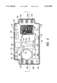
- FIGS. 1A, 1B, 1C and 1D show top, side, front and rear end views, respectively, of an adaptable planar module according to an embodiment of the invention.
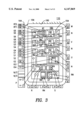
- FIG. 2 shows a top view of the module of FIGS. 1A-1D with the IMS exposed.
- FIG. 3 shows the IMS substrate and its interconnect to the PCB of FIG. 2 in greater detail.
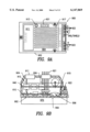
- FIG. 4A shows a cross-sectional view of the PCB of FIG. 2 taken along lines 4--4.
- FIG. 4B shows a top view of the PCB.
- FIGS. 5A and 5B show a top view and a cross-sectional view, respectively, of an adaptable planar module according to a further embodiment of the invention.
- FIGS. 6A and 6B respectively show a top view and a cross-sectional view, of a micro-inverter module according to another aspect of the invention.
- FIGS. 7A and 7B show a top view and a cross-sectional view, respectively, of a micro-inverter module according to still further embodiment of the invention.
- FIGS. 8A and 8B show a top view and cross-sectional view, respectively, of a micro-inverter module according to yet another embodiment of the invention.
- FIGS. 9A and 9B show respective top and cross-sectional views of an adaptable planar module according to another embodiment of the invention.
- FIGS. 10A and 10B show a top view and a cross-sectional view, respectively, of an adaptable planar module according to still further embodiment of the invention.
- FIG. 11 shows a top view of an adaptable planar module according to an additional embodiment of the invention.
- FIG. 12 shows a top view of a further arrangement of an IMS according to the invention.
- FIGS. 13A and 13B show respective top and side views of an example of a 1/2 HP motor control module which is capable of housing the IMS of FIG. 13.
- FIGS. 1A-1D an APM 100 according to an embodiment of the invention.
- the APM includes a support base 102 which supports a printed circuit board 110.
- a printed circuit board 110 Mounted atop printed circuit board 110 are various electrical components including choke 124, resistors 131, 132, capacitors 133, 134, 135, 136, 138, transformer 148, inductors 141 and 146 as well as additional circuit elements 140, 142 and 144 and other components, all of which are interconnected by printed wiring (not shown) on circuit board 110.
- I/O pins 127 and 129 and terminals 122A-122F which provide external connections to the circuit board.
- a support tray 166 rests atop circuit board 110 and supports capacitors 126 and 128 which are electrically connected to circuit board 110 and which are held in place by belt 130. Openings 137 and 139 extend through support tray 131, circuit board 110 and support base 102 for securing the APM.
- FIG. 2 shows the top view shown in FIG. 1A of APM 100 but with the support tray and its capacitors removed.
- An opening 160 formed in circuit board 110 is situated above an IMS 150.
- the support tray 166 is situated above opening 160 and IMS 150.
- Bonding pads 164 are arranged around the periphery of opening 160 and are electrically connected to the other components mounted on the board. Bonding wires 156 provide electrical connections between the bonding pads 164 of the circuit board and the components mounted on IMS 150.
- FIG. 3 shows the top view of the IMS as well as a portion of the circuit board 110 that surrounds opening 160 in greater detail.
- IMS 150 Mounted atop IMS 150 are various components including MOS-gate controlled power semiconductor devices Q1-Q6, diodes D1-D10 as well as resistors RT and RS1. Each of these components are thermally and electrically mounted atop portions of a conducting patterned material 154, such as copper. Also present, on the top surfaces of the devices, are bonding pad areas. Bonding wires 156 provide connections from the various components as well as from bonding pads 164 to the conducting pattern and the pad areas of the IMS components.
- FIG. 4A illustrates a cross-sectional view of the structure of FIG. 2.
- the IMS has a relatively thick body 152 formed of a conductive metal, such as aluminum, that is covered by a very thin insulation layer which, in turn, carries the conductive pattern which is electrically insulated from the body. Also present are heat spreaders (not shown) to which the components are mounted for improving thermal management of the heat generated by the components during their operation.
- An example of an IMS is described in the above-mentioned U.S. Pat. No. 5,408,128, which is incorporated herein by reference.
- the IMS is mounted in an opening of the support body 102 such that it is situated below the circuit board 110 and such that the bottom surface of the body 152 is located co-planar with or below the bottom surface 104 of support body 102 and is available for thermal contact with a heatsink (not shown).
- a heatsink (not shown).
- raised portions 106 and 108 which extends from support body 102 and support the circuit board 110 at the opening and periphery, respectively, of the circuit board 110.
- the raised portions 106 and the opening in the circuit board form a cavity above the IMS which is filled with a high grade potting material 158 to cover the top surface of the IMS.
- a lower grade, and less costly, potting material can then be used between the bottom surface of the circuit board and the support body as well as to cover at least a portion of the components mounted atop the circuit board.
- FIG. 4B shows an example of a circuit board 210 which is suitable for mounting components as well as having an opening 260 that is to be situated above the IMS and employed in the manner of the invention.
- the arrangement of the opening in the circuit board above the IMS minimizes the number and the length of the bonding wires that connect the components mounted atop the IMS and those mounted on the circuit board. Moreover, by mounting only the high power components on the IMS, the cost of the module is greatly reduced. Further, because both the high power and low power components are mounted in the same module, the footprint is greatly reduced, and the number of interconnections is further decreased. Additionally, by limiting the high grade potting compound to only the region atop the IMS, the cost of the module is also reduced.
- a cover such as a molded cover, (not shown) may be supplied atop the circuit board to cover the components of the circuit board and the IMS and is preferably supported by the periphery of the support base.
- FIGS. 5A and 5B show an example of appliance APM package 500 with no input/output filters in accordance with another embodiment of the invention.
- a molded shell support base 502 supports a printed circuit board 510 and has an opening through which IMS 550 is mounted. The bottom surface of the IMS 550 contacts heatsink 570 to remove heat from the power devices mounted atop the IMS, as described above. Also, an opening 560 formed in the circuit board is situated atop the IMS to minimize the length of the wire bonds.
- a high grade potting material 558 fills a cavity region above the IMS, and a lower grade potting material 559 is present elsewhere in the module.
- components 528 are mounted both on the top and bottom surfaces of the module.
- Bus capacitor 526 is mounted atop circuit board 510. Optionally, bus capacitor 526 can be mounted below circuit board 510 on the exterior of base 502, away from heatsink 570.
- the terminals 522 are fast-on connectors with in-line connector pins for providing control signals. Also shown are optional input/output pins 524.
- the typically 3.0" ⁇ 2.0" ⁇ 0.5" package can house a full motor control circuit, including an inverter circuit, input circuits, protection circuits and a microprocessor.
- the inverter and input circuits are located on the IMS 550, and other components 528 are located on the circuit board 510.
- the 3.0 inch length is a protective maximum size, though streamlined products may be smaller in size.
- FIGS. 6A and 6B show an example of a micro-inverter APM package 600 with full input/output filters according to a further embodiment of the invention.
- This embodiment is similar to the appliance APM 500 except that an additional printed circuit board 640 is added for supporting the inductors and capacitors of the input/output filters.
- the added board 640 is connected to board 610 by interconnect lead frame 615.
- the size of the added board and its components will vary with power rating of the APM, which ranges typically between 0.1 to 1.0 HP.
- FIGS. 6A and 6B show a simple shell with procured terminals 622.
- FIG. 7A and 7B show a substantially similar APM 700 with a shell 702 and integrated terminals 722. Note that with the procured terminals or the integrated terminals, the terminals are soldered to the main PCB with an isolated potting cavity. Optional input/output pins 624 are also shown.
- FIGS. 8A and 8B show an example of a micro-inverter APM package 800 with no filters in accordance with a still further embodiment of the invention.
- the package is similar to that of FIGS. 6A-6B and 7A-7B except the body height is reduced by the elimination of the added circuit board that otherwise holds the filter circuit. Instead, a bus capacitor 526 is mounted below the bottom surface of the base 802 but away from heatsink 870.
- FIGS. 8A and 8B show integrated shell terminals 822, the procured terminals are also an option.
- the APM packages of FIGS. 6A-6B, 7A-7B and 8A-8B can also be modified to accommodate a keyboard 612, 712 or 812, respectively, on the top surface of the PCB.
- the packages can also accommodate a lid which may provide EMI shielding.
- the filtering and package of the invention are designed to minimize filter size and have an architecture such that common tooling and processing can be used where possible for more than one embodiment of the APM.
- FIGS. 9A and 9B show top and cross-sectional views of an embodiment of a complete motor drive APM 900 with integrated terminals 922 in further accordance with the invention.
- a molded cover lid 904 is shown covering base 902 which includes an input/output connector 921, LED 913 and air vents 917.
- APM 900 further includes optional keyboard 911 protruding through an opening in cover lid 904. Keyboard 911 is coupled to circuit board 640 via connector 912. The bottom surface of IMS 550 contacts heatsink 970.
- FIGS. 10A-10B show another example of a top and cross-sectional views of a complete motor drive APM 901 with attached terminals 982 according to another embodiment of the invention.
- the attached terminals 982 are substituted in place of integrated terminals 922 shown in FIGS. 9A-9B.
- FIG. 11 shows a top view of another embodiment of a complete motor drive APM 1103 in accordance with the invention.
- integrated terminals 1122A and 1122B are located at opposite ends of the package and keyboard 1111 is positioned longitudinally with respect to the longer side of base 1102.
- Molded cover lid 1104 is adapted to accommodate optional keyboard 1111 and terminals 1122A and 1122B.
- FIG. 12 shows a further example of an IMS 1250 comprised of plural transistors, IGBTs, diodes and resistors which are interconnected as well as externally connected.
- FIGS. 13A and 13B illustrate an embodiment of a 1/2 HP motor control module and drive circuit APM module 1200 which is likewise in accordance with the invention.
- the module includes a base 1204, a driver PCB 1210 and houses an IMS 1250, such as is shown in FIG. 13, which is connected to the driver PCB by connector 1215.
- a control board 1240 may be included in the module and arranged atop the driver circuit board, and a further optional keyboard 1244 may be included and arranged atop the control board.
- Integrated terminals 1222 are positioned along one edge of module 1200.
- the module is extended in length so that control circuits may be included on an extended driver PCB 1210A positioned within an extended base 1204A.
- an extended keyboard 1244A may also be included in the module and arranged atop the extended circuit board.
- the novel features of the above embodiment of the APM of the invention allow these products to be manufactured at lower cost.
- the primary cost reduction features include: 1) minimized IMS substrate area, 2) a thinner IMS substrate, 3) no wire bonds on the IMS metalization, 3) all tracks on a double side PCB, 4) all substrate-to-IMS connections are wire bonds that are ordinarily otherwise present, 5) an integrated driver and microprocessor printed circuit board, 6) an integrated shell/terminal molding option, 7) a single package for all functions with potting to reduce size and UL creepage path limitations, and 8) compatible tooling for European and U.S. products for both micro-inverter and appliance products.
Abstract
Description
Claims (38)
Priority Applications (2)
| Application Number | Priority Date | Filing Date | Title |
|---|---|---|---|
| US09/197,078 US6147869A (en) | 1997-11-24 | 1998-11-20 | Adaptable planar module |
| US09/632,026 US6272015B1 (en) | 1997-11-24 | 2000-08-02 | Power semiconductor module with insulation shell support for plural separate substrates |
Applications Claiming Priority (2)
| Application Number | Priority Date | Filing Date | Title |
|---|---|---|---|
| US6645297P | 1997-11-24 | 1997-11-24 | |
| US09/197,078 US6147869A (en) | 1997-11-24 | 1998-11-20 | Adaptable planar module |
Related Child Applications (1)
| Application Number | Title | Priority Date | Filing Date |
|---|---|---|---|
| US09/632,026 Division US6272015B1 (en) | 1997-11-24 | 2000-08-02 | Power semiconductor module with insulation shell support for plural separate substrates |
Publications (1)
| Publication Number | Publication Date |
|---|---|
| US6147869A true US6147869A (en) | 2000-11-14 |
Family
ID=22069594
Family Applications (2)
| Application Number | Title | Priority Date | Filing Date |
|---|---|---|---|
| US09/197,078 Expired - Fee Related US6147869A (en) | 1997-11-24 | 1998-11-20 | Adaptable planar module |
| US09/632,026 Expired - Lifetime US6272015B1 (en) | 1997-11-24 | 2000-08-02 | Power semiconductor module with insulation shell support for plural separate substrates |
Family Applications After (1)
| Application Number | Title | Priority Date | Filing Date |
|---|---|---|---|
| US09/632,026 Expired - Lifetime US6272015B1 (en) | 1997-11-24 | 2000-08-02 | Power semiconductor module with insulation shell support for plural separate substrates |
Country Status (4)
| Country | Link |
|---|---|
| US (2) | US6147869A (en) |
| JP (1) | JP3222848B2 (en) |
| DE (1) | DE19854180B4 (en) |
| FR (1) | FR2773301B1 (en) |
Cited By (36)
| Publication number | Priority date | Publication date | Assignee | Title |
|---|---|---|---|---|
| US6362964B1 (en) * | 1999-11-17 | 2002-03-26 | International Rectifier Corp. | Flexible power assembly |
| US6377465B1 (en) * | 1999-01-14 | 2002-04-23 | Nec Corporation | Printing wiring board |
| US6429507B1 (en) * | 2000-04-03 | 2002-08-06 | Artesyn Technologies, Inc. | Electrical device including a leaded cell assembly |
| US6441509B1 (en) * | 1997-11-20 | 2002-08-27 | Sevcon Limited | Controller for battery-operated vehicle |
| US20020167828A1 (en) * | 2000-09-20 | 2002-11-14 | Ballard Power Systems Corporation | Leadframe-based module DC bus design to reduce module inductance |
| US6491528B1 (en) * | 1998-12-24 | 2002-12-10 | At&T Wireless Services, Inc. | Method and apparatus for vibration and temperature isolation |
| US20020191381A1 (en) * | 2001-06-15 | 2002-12-19 | Kabushiki Kaisha Sankyo Seiki Seisakusho | Tape running apparatus, motor board, and capstan motor |
| US6549409B1 (en) * | 2000-08-21 | 2003-04-15 | Vlt Corporation | Power converter assembly |
| US6560110B1 (en) * | 2002-02-22 | 2003-05-06 | Delphi Technologies, Inc. | Corrosive resistant flip chip thermal management structure |
| US20040056631A1 (en) * | 2002-09-23 | 2004-03-25 | James Derksen | System and method for improved motor controller |
| US20050280998A1 (en) * | 2004-06-18 | 2005-12-22 | Heny Lin | Half-bridge power module with insert molded heatsinks |
| US20060061937A1 (en) * | 2003-09-18 | 2006-03-23 | Junji Takemoto | Capacitor unit |
| US20060252179A1 (en) * | 2005-05-06 | 2006-11-09 | Neobulb Technologies, Inc. | Integrated circuit packaging structure and method of making the same |
| US20070139895A1 (en) * | 2005-11-04 | 2007-06-21 | Reis Bradley E | LED with integral thermal via |
| US20070249188A1 (en) * | 2004-01-30 | 2007-10-25 | Robert Bosch Gmbh | Device for the Shakeproof Accomodation of Electrical Special Components and/or Electrical Circuits |
| US20080158824A1 (en) * | 2006-12-27 | 2008-07-03 | Aisin Aw Co., Ltd. | Electric circuit device and the manufacturing method |
| US20090086431A1 (en) * | 2007-09-27 | 2009-04-02 | Sanyo Electric Co., Ltd. | Circuit device, circuit module, and outdoor unit |
| US20090086442A1 (en) * | 2007-09-27 | 2009-04-02 | Sanyo Electric Co., Ltd. | Circuit module |
| US20090086455A1 (en) * | 2007-09-27 | 2009-04-02 | Sanyo Electric Co., Ltd. | Circuit device and method of manufacturing the same |
| US20090086454A1 (en) * | 2007-09-27 | 2009-04-02 | Sanyo Electric Co., Ltd. | Circuit device |
| US20090103276A1 (en) * | 2007-09-27 | 2009-04-23 | Sanyo Electric Co., Ltd. | Circuit device and method of manufacturing the same |
| US20090180262A1 (en) * | 2008-01-11 | 2009-07-16 | Sma Solar Technology Ag | Inverter |
| DE10196942B4 (en) * | 2001-05-30 | 2009-09-03 | International Rectifier Corp., El Segundo | Semiconductor power module |
| US20090266597A1 (en) * | 2008-04-28 | 2009-10-29 | Hon Hai Precision Industry Co., Ltd. | Printed circuit board preform with test facilitating means |
| US20100043222A1 (en) * | 2008-03-31 | 2010-02-25 | Josh Wurzel | Conforming, electro-magnetic interference reducing cover for circuit components |
| US7889502B1 (en) * | 2005-11-04 | 2011-02-15 | Graftech International Holdings Inc. | Heat spreading circuit assembly |
| US20110286184A1 (en) * | 2010-05-19 | 2011-11-24 | Debabrata Pal | Thermal packaging of a motor controller for an auxiliary power unit |
| FR2979177A1 (en) * | 2011-08-19 | 2013-02-22 | Valeo Sys Controle Moteur Sas | POWER BLOCK FOR ELECTRIC VEHICLE INVERTER |
| US20130293047A1 (en) * | 2011-02-22 | 2013-11-07 | Keiji Nagasaka | Integrated-inverter electric compressor |
| US20140334105A1 (en) * | 2013-05-09 | 2014-11-13 | Ford Global Technologies, Llc | Integrated Electrical and Thermal Solution for Inverter DC-Link Capacitor Packaging |
| CN105308847A (en) * | 2013-06-19 | 2016-02-03 | 株式会社日立产机系统 | Power conversion device |
| US20160039266A1 (en) * | 2013-03-26 | 2016-02-11 | Valeo Systemes Thermiques | Control module for an electric appliance |
| USD768570S1 (en) | 2014-04-25 | 2016-10-11 | Colgate-Palmolive Company | Charger for electric toothbrush |
| USD768571S1 (en) | 2014-04-25 | 2016-10-11 | Colgate-Palmolive Company | Charger for electric toothbrush |
| US9853524B2 (en) | 2014-07-29 | 2017-12-26 | Regal Beloit America, Inc. | Motor and controller with isolation members between electrical components and associated method |
| US20220396154A1 (en) * | 2021-06-14 | 2022-12-15 | Panasonic Intellectual Property Management Co., Ltd. | Vehicle mounted electric power converter |
Families Citing this family (101)
| Publication number | Priority date | Publication date | Assignee | Title |
|---|---|---|---|---|
| US6819095B1 (en) * | 1999-09-16 | 2004-11-16 | International Rectifier Corporation | Power semiconductor device assembly with integrated current sensing and control |
| DE10191585B8 (en) * | 2000-04-25 | 2009-07-02 | Kabushiki Kaisha Toyota Jidoshokki, Kariya | Semiconductor device |
| KR100403608B1 (en) * | 2000-11-10 | 2003-11-01 | 페어차일드코리아반도체 주식회사 | Stacked intelligent power module package and manufacturing method thereof |
| DE10102834A1 (en) * | 2001-01-22 | 2002-08-01 | Bosch Gmbh Robert | Electrical device, in particular switching or control device for motor vehicles |
| US6740968B2 (en) * | 2001-03-12 | 2004-05-25 | Matsushita Electric Industrial Co., Ltd. | Power source unit for driving magnetron and heatsink to be mounted on printed circuit board thereof |
| US7046518B2 (en) * | 2001-04-02 | 2006-05-16 | International Rectifier Corporation | Power module |
| EP1318547B1 (en) * | 2001-12-06 | 2013-04-17 | ABB Research Ltd. | Power semiconductor module |
| WO2003071601A2 (en) * | 2002-02-18 | 2003-08-28 | Infineon Technologies Ag | Circuit module and method for the production thereof |
| US20040067695A1 (en) * | 2002-10-02 | 2004-04-08 | Marceau Scott P. | Electrical connector assembly |
| EP1453366A1 (en) * | 2003-02-28 | 2004-09-01 | Siemens Aktiengesellschaft | Electronic device with improved heat dissipation |
| US6775145B1 (en) * | 2003-05-14 | 2004-08-10 | Cyntec Co., Ltd. | Construction for high density power module package (case II) |
| US7250672B2 (en) * | 2003-11-13 | 2007-07-31 | International Rectifier Corporation | Dual semiconductor die package with reverse lead form |
| JP4284531B2 (en) * | 2004-07-06 | 2009-06-24 | オムロン株式会社 | Mounting board and driving device using the same |
| US7885076B2 (en) * | 2004-09-07 | 2011-02-08 | Flextronics Ap, Llc | Apparatus for and method of cooling molded electronic circuits |
| JP4453498B2 (en) * | 2004-09-22 | 2010-04-21 | 富士電機システムズ株式会社 | Power semiconductor module and manufacturing method thereof |
| JP2006173969A (en) * | 2004-12-15 | 2006-06-29 | Sony Corp | Omnidirectional light reception device and infrared receiving device |
| WO2006063539A1 (en) * | 2004-12-17 | 2006-06-22 | Siemens Aktiengesellschaft | Semiconductor switching module |
| JP4374312B2 (en) * | 2004-12-21 | 2009-12-02 | 三菱電機株式会社 | Assembly method of semiconductor switching element and heat sink in in-vehicle rotating electrical machine and in-vehicle rotating electrical machine |
| WO2007025252A1 (en) * | 2005-08-26 | 2007-03-01 | Tk Holdings Inc. | Electronic module and method for sealing an electronic module |
| DE102005050028A1 (en) * | 2005-10-14 | 2007-04-19 | Robert Bosch Gmbh | Electric device, in particular for controlling a motor and / or regenerative electric machine |
| JP4227987B2 (en) * | 2005-12-01 | 2009-02-18 | 三菱電機株式会社 | Rotating electric machine and manufacturing method thereof |
| US7989981B2 (en) * | 2006-02-02 | 2011-08-02 | Flextronics Ap, Llc | Power adaptor and storage unit for portable devices |
| JP5420910B2 (en) * | 2006-02-14 | 2014-02-19 | フレクストロニクス エーピー,リミテッド ライアビリティ カンパニー | Power converter |
| DE102006018854A1 (en) * | 2006-04-22 | 2007-11-22 | Sma Technologie Ag | Housing of a power converter |
| DE102006040686B4 (en) * | 2006-08-30 | 2013-01-31 | Insta Elektro Gmbh | Electrical / electronic installation device |
| CN101636702B (en) * | 2006-09-25 | 2014-03-05 | 弗莱克斯电子有限责任公司 | Bi-directional regulator |
| DE102007002342B3 (en) * | 2007-01-16 | 2008-10-16 | Friwo Mobile Power Gmbh | Simplified primary-side drive circuit for the switch in a switching power supply |
| US7760519B2 (en) * | 2007-03-29 | 2010-07-20 | Flextronics Ap, Llc | Primary only control quasi resonant convertor |
| US7830676B2 (en) * | 2007-03-29 | 2010-11-09 | Flextronics Ap, Llc | Primary only constant voltage/constant current (CVCC) control in quasi resonant convertor |
| US8191241B2 (en) * | 2007-03-29 | 2012-06-05 | Flextronics Ap, Llc | Method of producing a multi-turn coil from folded flexible circuitry |
| US7755914B2 (en) * | 2007-03-29 | 2010-07-13 | Flextronics Ap, Llc | Pulse frequency to voltage conversion |
| US7978489B1 (en) | 2007-08-03 | 2011-07-12 | Flextronics Ap, Llc | Integrated power converters |
| US7920039B2 (en) * | 2007-09-25 | 2011-04-05 | Flextronics Ap, Llc | Thermally enhanced magnetic transformer |
| EP2051360B1 (en) * | 2007-10-17 | 2016-09-21 | Power Systems Technologies GmbH | Control circuit for a primary controlled switching power supply with increased accuracy of voltage regulation and primary controlled switched mode power supply |
| US8279646B1 (en) | 2007-12-14 | 2012-10-02 | Flextronics Ap, Llc | Coordinated power sequencing to limit inrush currents and ensure optimum filtering |
| US8693213B2 (en) * | 2008-05-21 | 2014-04-08 | Flextronics Ap, Llc | Resonant power factor correction converter |
| US8102678B2 (en) * | 2008-05-21 | 2012-01-24 | Flextronics Ap, Llc | High power factor isolated buck-type power factor correction converter |
| US8975523B2 (en) * | 2008-05-28 | 2015-03-10 | Flextronics Ap, Llc | Optimized litz wire |
| US8531174B2 (en) * | 2008-06-12 | 2013-09-10 | Flextronics Ap, Llc | AC-DC input adapter |
| JPWO2010024233A1 (en) * | 2008-08-27 | 2012-01-26 | 日本電気株式会社 | Wiring board capable of incorporating functional elements and method for manufacturing the same |
| US8081019B2 (en) * | 2008-11-21 | 2011-12-20 | Flextronics Ap, Llc | Variable PFC and grid-tied bus voltage control |
| US8237260B2 (en) * | 2008-11-26 | 2012-08-07 | Infineon Technologies Ag | Power semiconductor module with segmented base plate |
| US8787044B2 (en) * | 2009-05-07 | 2014-07-22 | Flextronics Ap, Llc | Energy recovery snubber circuit for power converters |
| US8040117B2 (en) * | 2009-05-15 | 2011-10-18 | Flextronics Ap, Llc | Closed loop negative feedback system with low frequency modulated gain |
| US8891803B2 (en) * | 2009-06-23 | 2014-11-18 | Flextronics Ap, Llc | Notebook power supply with integrated subwoofer |
| US8289741B2 (en) * | 2010-01-14 | 2012-10-16 | Flextronics Ap, Llc | Line switcher for power converters |
| US8586873B2 (en) * | 2010-02-23 | 2013-11-19 | Flextronics Ap, Llc | Test point design for a high speed bus |
| US8964413B2 (en) | 2010-04-22 | 2015-02-24 | Flextronics Ap, Llc | Two stage resonant converter enabling soft-switching in an isolated stage |
| US8488340B2 (en) | 2010-08-27 | 2013-07-16 | Flextronics Ap, Llc | Power converter with boost-buck-buck configuration utilizing an intermediate power regulating circuit |
| US9362205B2 (en) * | 2010-09-24 | 2016-06-07 | Semiconductor Components Industries, Llc | Circuit device |
| US8441810B2 (en) | 2010-11-09 | 2013-05-14 | Flextronics Ap, Llc | Cascade power system architecture |
| US8520410B2 (en) | 2010-11-09 | 2013-08-27 | Flextronics Ap, Llc | Virtual parametric high side MOSFET driver |
| DE102011013368B4 (en) | 2011-03-08 | 2024-02-01 | Diehl Aerospace Gmbh | Passenger service unit, passenger service channel and means of transport |
| US8842450B2 (en) | 2011-04-12 | 2014-09-23 | Flextronics, Ap, Llc | Power converter using multiple phase-shifting quasi-resonant converters |
| CN103688126A (en) | 2011-07-12 | 2014-03-26 | 弗莱克斯电子有限责任公司 | Heat transfer system with integrated evaporator and condenser |
| US9117991B1 (en) | 2012-02-10 | 2015-08-25 | Flextronics Ap, Llc | Use of flexible circuits incorporating a heat spreading layer and the rigidizing specific areas within such a construction by creating stiffening structures within said circuits by either folding, bending, forming or combinations thereof |
| US9232630B1 (en) | 2012-05-18 | 2016-01-05 | Flextronics Ap, Llc | Method of making an inlay PCB with embedded coin |
| JP5948668B2 (en) * | 2012-05-22 | 2016-07-06 | パナソニックIpマネジメント株式会社 | Semiconductor device and manufacturing method thereof |
| US9276460B2 (en) | 2012-05-25 | 2016-03-01 | Flextronics Ap, Llc | Power converter with noise immunity |
| US9203292B2 (en) | 2012-06-11 | 2015-12-01 | Power Systems Technologies Ltd. | Electromagnetic interference emission suppressor |
| US9203293B2 (en) | 2012-06-11 | 2015-12-01 | Power Systems Technologies Ltd. | Method of suppressing electromagnetic interference emission |
| US9366394B2 (en) | 2012-06-27 | 2016-06-14 | Flextronics Ap, Llc | Automotive LED headlight cooling system |
| US9019726B2 (en) | 2012-07-13 | 2015-04-28 | Flextronics Ap, Llc | Power converters with quasi-zero power consumption |
| US8743565B2 (en) | 2012-07-27 | 2014-06-03 | Flextronics Ap, Llc | High power converter architecture |
| US9019724B2 (en) | 2012-07-27 | 2015-04-28 | Flextronics Ap, Llc | High power converter architecture |
| US9287792B2 (en) | 2012-08-13 | 2016-03-15 | Flextronics Ap, Llc | Control method to reduce switching loss on MOSFET |
| US9118253B2 (en) | 2012-08-15 | 2015-08-25 | Flextronics Ap, Llc | Energy conversion architecture with secondary side control delivered across transformer element |
| US9318965B2 (en) | 2012-10-10 | 2016-04-19 | Flextronics Ap, Llc | Method to control a minimum pulsewidth in a switch mode power supply |
| US9605860B2 (en) | 2012-11-02 | 2017-03-28 | Flextronics Ap, Llc | Energy saving-exhaust control and auto shut off system |
| US9092712B2 (en) | 2012-11-02 | 2015-07-28 | Flextronics Ap, Llc | Embedded high frequency RFID |
| US9660540B2 (en) | 2012-11-05 | 2017-05-23 | Flextronics Ap, Llc | Digital error signal comparator |
| WO2014088974A1 (en) | 2012-12-03 | 2014-06-12 | Flextronics Ap, Llc | Driving board folding machine |
| KR101443985B1 (en) * | 2012-12-14 | 2014-11-03 | 삼성전기주식회사 | Power module package |
| US9171809B2 (en) | 2013-03-05 | 2015-10-27 | Flextronics Ap, Llc | Escape routes |
| US9494658B2 (en) | 2013-03-14 | 2016-11-15 | Flextronics Ap, Llc | Approach for generation of power failure warning signal to maximize useable hold-up time with AC/DC rectifiers |
| US9323267B2 (en) | 2013-03-14 | 2016-04-26 | Flextronics Ap, Llc | Method and implementation for eliminating random pulse during power up of digital signal controller |
| US9490651B2 (en) | 2013-03-15 | 2016-11-08 | Flextronics Ap, Llc | Sweep frequency mode for magnetic resonant power transmission |
| US8654553B1 (en) | 2013-03-15 | 2014-02-18 | Flextronics Ap, Llc | Adaptive digital control of power factor correction front end |
| US9184668B2 (en) | 2013-03-15 | 2015-11-10 | Flextronics Ap, Llc | Power management integrated circuit partitioning with dedicated primary side control winding |
| US9093911B2 (en) | 2013-03-15 | 2015-07-28 | Flextronics Ap, Llc | Switching mode power converter using coded signal control |
| DE102013010843A1 (en) * | 2013-06-28 | 2014-12-31 | Wabco Gmbh | Electric control unit |
| WO2015007507A1 (en) | 2013-07-15 | 2015-01-22 | Abb Technology Ag | Power semiconductor module |
| US9521754B1 (en) | 2013-08-19 | 2016-12-13 | Multek Technologies Limited | Embedded components in a substrate |
| US9801277B1 (en) | 2013-08-27 | 2017-10-24 | Flextronics Ap, Llc | Bellows interconnect |
| US9053405B1 (en) | 2013-08-27 | 2015-06-09 | Flextronics Ap, Llc | Printed RFID circuit |
| US9565748B2 (en) | 2013-10-28 | 2017-02-07 | Flextronics Ap, Llc | Nano-copper solder for filling thermal vias |
| US9338915B1 (en) | 2013-12-09 | 2016-05-10 | Flextronics Ap, Llc | Method of attaching electronic module on fabrics by stitching plated through holes |
| US9549463B1 (en) | 2014-05-16 | 2017-01-17 | Multek Technologies, Ltd. | Rigid to flexible PC transition |
| US9723713B1 (en) | 2014-05-16 | 2017-08-01 | Multek Technologies, Ltd. | Flexible printed circuit board hinge |
| US9621053B1 (en) | 2014-08-05 | 2017-04-11 | Flextronics Ap, Llc | Peak power control technique for primary side controller operation in continuous conduction mode |
| US9661738B1 (en) | 2014-09-03 | 2017-05-23 | Flextronics Ap, Llc | Embedded coins for HDI or SEQ laminations |
| US10123603B1 (en) | 2015-03-27 | 2018-11-13 | Multek Technologies Limited | Diffuse fiber optic lighting for luggage |
| US10154583B1 (en) | 2015-03-27 | 2018-12-11 | Flex Ltd | Mechanical strain reduction on flexible and rigid-flexible circuits |
| DE102015219947A1 (en) * | 2015-10-14 | 2017-04-20 | Zf Friedrichshafen Ag | Circuit carrier and method for producing the same |
| US10321560B2 (en) | 2015-11-12 | 2019-06-11 | Multek Technologies Limited | Dummy core plus plating resist restrict resin process and structure |
| US10064292B2 (en) | 2016-03-21 | 2018-08-28 | Multek Technologies Limited | Recessed cavity in printed circuit board protected by LPI |
| US10712398B1 (en) | 2016-06-21 | 2020-07-14 | Multek Technologies Limited | Measuring complex PCB-based interconnects in a production environment |
| JP6432712B2 (en) * | 2016-07-11 | 2018-12-05 | 三菱電機株式会社 | Semiconductor device |
| EP3382378B1 (en) * | 2017-03-29 | 2022-10-26 | Mitsubishi Electric R&D Centre Europe B.V. | Optical monitoring |
| KR102477829B1 (en) * | 2019-04-12 | 2022-12-15 | 삼성전자 주식회사 | A converter including a printed circuit board and power converting module including the converter |
| GB2602340B (en) * | 2020-12-23 | 2024-04-03 | Yasa Ltd | Semiconductor cooling arrangement with improved heatsink |
Citations (22)
| Publication number | Priority date | Publication date | Assignee | Title |
|---|---|---|---|---|
| US4899256A (en) * | 1988-06-01 | 1990-02-06 | Chrysler Motors Corporation | Power module |
| US4965710A (en) * | 1989-11-16 | 1990-10-23 | International Rectifier Corporation | Insulated gate bipolar transistor power module |
| JPH03272163A (en) * | 1990-03-22 | 1991-12-03 | Nippondenso Co Ltd | Hybrid integrated circuit |
| JPH05304248A (en) * | 1991-12-10 | 1993-11-16 | Fuji Electric Co Ltd | Semiconductor device |
| US5353194A (en) * | 1991-04-30 | 1994-10-04 | Sgs-Thomson Microelectronics S.R.L. | Modular power circuit assembly |
| US5373418A (en) * | 1990-03-28 | 1994-12-13 | Mitsubishi Denki Kabushiki Kaisha | Electrical device for mounting electrical components with enhanced thermal radiating properties |
| US5398160A (en) * | 1992-10-20 | 1995-03-14 | Fujitsu General Limited | Compact power module with a heat spreader |
| US5408128A (en) * | 1993-09-15 | 1995-04-18 | International Rectifier Corporation | High power semiconductor device module with low thermal resistance and simplified manufacturing |
| US5408383A (en) * | 1991-05-31 | 1995-04-18 | Nippondenso Co., Ltd. | Container for electronic devices having a plurality of circuit boards |
| US5450288A (en) * | 1990-11-06 | 1995-09-12 | Oki Electric Industry Co., Ltd. | Printed substrate for mounting high-power semiconductor chip thereon and driver component making use of the printed substrate |
| US5521437A (en) * | 1993-07-05 | 1996-05-28 | Mitsubishi Denki Kabushiki Kaisha | Semiconductor power module having an improved composite board and method of fabricating the same |
| US5536972A (en) * | 1993-12-09 | 1996-07-16 | Mitsubishi Denki Kabushiki Kaisha | Power module |
| US5576934A (en) * | 1992-07-09 | 1996-11-19 | Robert Bosch Gmbh | Mounting unit for a multilayer hybrid circuit having power components including a copper coated ceramic center board |
| JPH098223A (en) * | 1995-06-16 | 1997-01-10 | Mitsubishi Electric Corp | Semiconductor power module and its manufacture |
| US5606487A (en) * | 1990-07-18 | 1997-02-25 | Hitachi, Ltd. | Electronic device for offsetting adverse effects of a plurality of chips which repetitively produce large pulses of heat |
| US5616888A (en) * | 1995-09-29 | 1997-04-01 | Allen-Bradley Company, Inc. | Rigid-flex circuit board having a window for an insulated mounting area |
| US5625536A (en) * | 1994-12-08 | 1997-04-29 | Fuji Electric Co., Ltd. | Semiconductor device |
| US5646827A (en) * | 1991-05-31 | 1997-07-08 | Nippondenso Co., Ltd. | Electronic device having a plurality of circuit boards arranged therein |
| US5657203A (en) * | 1991-05-31 | 1997-08-12 | Nippondenso Co., Ltd. | Electronic device having a plurality of circuit boards arranged therein |
| US5689091A (en) * | 1996-09-19 | 1997-11-18 | Vlsi Technology, Inc. | Multi-layer substrate structure |
| US5747876A (en) * | 1995-11-30 | 1998-05-05 | Mitsubishi Denki Kabushiki Kaisha | Semiconductor device and semiconductor module |
| US5825625A (en) * | 1996-05-20 | 1998-10-20 | Hewlett-Packard Company | Heat conductive substrate mounted in PC board for transferring heat from IC to heat sink |
Family Cites Families (8)
| Publication number | Priority date | Publication date | Assignee | Title |
|---|---|---|---|---|
| DE3916899C2 (en) * | 1989-05-24 | 2003-04-03 | Bosch Gmbh Robert | Housing for an electronic circuit |
| US5031069A (en) * | 1989-12-28 | 1991-07-09 | Sundstrand Corporation | Integration of ceramic capacitor |
| GB2249869B (en) * | 1990-09-17 | 1994-10-12 | Fuji Electric Co Ltd | Semiconductor device |
| DE4232575A1 (en) * | 1992-09-29 | 1994-03-31 | Bosch Gmbh Robert | Arrangement with a printed circuit board, at least one power component and a heat sink |
| JP2809026B2 (en) * | 1992-09-30 | 1998-10-08 | 三菱電機株式会社 | INVERTER DEVICE AND METHOD OF USING INVERTER DEVICE |
| DE4418426B4 (en) * | 1993-09-08 | 2007-08-02 | Mitsubishi Denki K.K. | Semiconductor power module and method of manufacturing the semiconductor power module |
| US5467251A (en) * | 1993-10-08 | 1995-11-14 | Northern Telecom Limited | Printed circuit boards and heat sink structures |
| DE19602637C1 (en) * | 1996-01-25 | 1997-07-24 | Siemens Ag | Control device, esp. for motor vehicle |
-
1998
- 1998-11-20 US US09/197,078 patent/US6147869A/en not_active Expired - Fee Related
- 1998-11-24 JP JP33325898A patent/JP3222848B2/en not_active Expired - Fee Related
- 1998-11-24 FR FR9814758A patent/FR2773301B1/en not_active Expired - Fee Related
- 1998-11-24 DE DE1998154180 patent/DE19854180B4/en not_active Expired - Fee Related
-
2000
- 2000-08-02 US US09/632,026 patent/US6272015B1/en not_active Expired - Lifetime
Patent Citations (22)
| Publication number | Priority date | Publication date | Assignee | Title |
|---|---|---|---|---|
| US4899256A (en) * | 1988-06-01 | 1990-02-06 | Chrysler Motors Corporation | Power module |
| US4965710A (en) * | 1989-11-16 | 1990-10-23 | International Rectifier Corporation | Insulated gate bipolar transistor power module |
| JPH03272163A (en) * | 1990-03-22 | 1991-12-03 | Nippondenso Co Ltd | Hybrid integrated circuit |
| US5373418A (en) * | 1990-03-28 | 1994-12-13 | Mitsubishi Denki Kabushiki Kaisha | Electrical device for mounting electrical components with enhanced thermal radiating properties |
| US5606487A (en) * | 1990-07-18 | 1997-02-25 | Hitachi, Ltd. | Electronic device for offsetting adverse effects of a plurality of chips which repetitively produce large pulses of heat |
| US5450288A (en) * | 1990-11-06 | 1995-09-12 | Oki Electric Industry Co., Ltd. | Printed substrate for mounting high-power semiconductor chip thereon and driver component making use of the printed substrate |
| US5353194A (en) * | 1991-04-30 | 1994-10-04 | Sgs-Thomson Microelectronics S.R.L. | Modular power circuit assembly |
| US5646827A (en) * | 1991-05-31 | 1997-07-08 | Nippondenso Co., Ltd. | Electronic device having a plurality of circuit boards arranged therein |
| US5657203A (en) * | 1991-05-31 | 1997-08-12 | Nippondenso Co., Ltd. | Electronic device having a plurality of circuit boards arranged therein |
| US5408383A (en) * | 1991-05-31 | 1995-04-18 | Nippondenso Co., Ltd. | Container for electronic devices having a plurality of circuit boards |
| JPH05304248A (en) * | 1991-12-10 | 1993-11-16 | Fuji Electric Co Ltd | Semiconductor device |
| US5576934A (en) * | 1992-07-09 | 1996-11-19 | Robert Bosch Gmbh | Mounting unit for a multilayer hybrid circuit having power components including a copper coated ceramic center board |
| US5398160A (en) * | 1992-10-20 | 1995-03-14 | Fujitsu General Limited | Compact power module with a heat spreader |
| US5521437A (en) * | 1993-07-05 | 1996-05-28 | Mitsubishi Denki Kabushiki Kaisha | Semiconductor power module having an improved composite board and method of fabricating the same |
| US5408128A (en) * | 1993-09-15 | 1995-04-18 | International Rectifier Corporation | High power semiconductor device module with low thermal resistance and simplified manufacturing |
| US5536972A (en) * | 1993-12-09 | 1996-07-16 | Mitsubishi Denki Kabushiki Kaisha | Power module |
| US5625536A (en) * | 1994-12-08 | 1997-04-29 | Fuji Electric Co., Ltd. | Semiconductor device |
| JPH098223A (en) * | 1995-06-16 | 1997-01-10 | Mitsubishi Electric Corp | Semiconductor power module and its manufacture |
| US5616888A (en) * | 1995-09-29 | 1997-04-01 | Allen-Bradley Company, Inc. | Rigid-flex circuit board having a window for an insulated mounting area |
| US5747876A (en) * | 1995-11-30 | 1998-05-05 | Mitsubishi Denki Kabushiki Kaisha | Semiconductor device and semiconductor module |
| US5825625A (en) * | 1996-05-20 | 1998-10-20 | Hewlett-Packard Company | Heat conductive substrate mounted in PC board for transferring heat from IC to heat sink |
| US5689091A (en) * | 1996-09-19 | 1997-11-18 | Vlsi Technology, Inc. | Multi-layer substrate structure |
Cited By (65)
| Publication number | Priority date | Publication date | Assignee | Title |
|---|---|---|---|---|
| US6441509B1 (en) * | 1997-11-20 | 2002-08-27 | Sevcon Limited | Controller for battery-operated vehicle |
| US6491528B1 (en) * | 1998-12-24 | 2002-12-10 | At&T Wireless Services, Inc. | Method and apparatus for vibration and temperature isolation |
| US6377465B1 (en) * | 1999-01-14 | 2002-04-23 | Nec Corporation | Printing wiring board |
| US6362964B1 (en) * | 1999-11-17 | 2002-03-26 | International Rectifier Corp. | Flexible power assembly |
| US6429507B1 (en) * | 2000-04-03 | 2002-08-06 | Artesyn Technologies, Inc. | Electrical device including a leaded cell assembly |
| US6549409B1 (en) * | 2000-08-21 | 2003-04-15 | Vlt Corporation | Power converter assembly |
| US7193860B2 (en) | 2000-09-20 | 2007-03-20 | Ballard Power Systems Corporation | Leadframe-based module DC bus design to reduce module inductance |
| US20020167828A1 (en) * | 2000-09-20 | 2002-11-14 | Ballard Power Systems Corporation | Leadframe-based module DC bus design to reduce module inductance |
| US20060028806A1 (en) * | 2000-09-20 | 2006-02-09 | Scott Parkhill | Leadframe-based module DC bus design to reduce module inductance |
| US7187558B2 (en) | 2000-09-20 | 2007-03-06 | Ballard Power Systems Corporation | Leadframe-based module DC bus design to reduce module inductance |
| US20060082983A1 (en) * | 2000-09-20 | 2006-04-20 | Scott Parkhill | Leadframe-based module DC bus design to reduce module inductance |
| US7012810B2 (en) * | 2000-09-20 | 2006-03-14 | Ballard Power Systems Corporation | Leadframe-based module DC bus design to reduce module inductance |
| DE10196942B4 (en) * | 2001-05-30 | 2009-09-03 | International Rectifier Corp., El Segundo | Semiconductor power module |
| US6791824B2 (en) * | 2001-06-15 | 2004-09-14 | Kabushiki Kaisha Sankyo Seiki Seisakusho | Tape running apparatus, motor board, and capstan motor |
| US20020191381A1 (en) * | 2001-06-15 | 2002-12-19 | Kabushiki Kaisha Sankyo Seiki Seisakusho | Tape running apparatus, motor board, and capstan motor |
| US6560110B1 (en) * | 2002-02-22 | 2003-05-06 | Delphi Technologies, Inc. | Corrosive resistant flip chip thermal management structure |
| US6891725B2 (en) * | 2002-09-23 | 2005-05-10 | Siemens Energy & Automation, Inc. | System and method for improved motor controller |
| US20040056631A1 (en) * | 2002-09-23 | 2004-03-25 | James Derksen | System and method for improved motor controller |
| US20060061937A1 (en) * | 2003-09-18 | 2006-03-23 | Junji Takemoto | Capacitor unit |
| US7427851B2 (en) * | 2003-09-18 | 2008-09-23 | Matsushita Electric Industrial Co., Ltd. | Capacitor unit |
| US20070249188A1 (en) * | 2004-01-30 | 2007-10-25 | Robert Bosch Gmbh | Device for the Shakeproof Accomodation of Electrical Special Components and/or Electrical Circuits |
| US7149088B2 (en) * | 2004-06-18 | 2006-12-12 | International Rectifier Corporation | Half-bridge power module with insert molded heatsinks |
| US20050280998A1 (en) * | 2004-06-18 | 2005-12-22 | Heny Lin | Half-bridge power module with insert molded heatsinks |
| US7948767B2 (en) | 2005-05-06 | 2011-05-24 | Neobulb Technologies, LLP. | Integrated circuit packaging structure and method of making the same |
| US20100140791A1 (en) * | 2005-05-06 | 2010-06-10 | Neobulb Technologies, Inc. | Integrated circuit packaging structure and method of making the same |
| US20060252179A1 (en) * | 2005-05-06 | 2006-11-09 | Neobulb Technologies, Inc. | Integrated circuit packaging structure and method of making the same |
| US20070139895A1 (en) * | 2005-11-04 | 2007-06-21 | Reis Bradley E | LED with integral thermal via |
| US7505275B2 (en) * | 2005-11-04 | 2009-03-17 | Graftech International Holdings Inc. | LED with integral via |
| US7889502B1 (en) * | 2005-11-04 | 2011-02-15 | Graftech International Holdings Inc. | Heat spreading circuit assembly |
| US20080158824A1 (en) * | 2006-12-27 | 2008-07-03 | Aisin Aw Co., Ltd. | Electric circuit device and the manufacturing method |
| US7663886B2 (en) * | 2006-12-27 | 2010-02-16 | Aisin Aw Co., Ltd. | Electric circuit device and the manufacturing method |
| US20090086455A1 (en) * | 2007-09-27 | 2009-04-02 | Sanyo Electric Co., Ltd. | Circuit device and method of manufacturing the same |
| US20090103276A1 (en) * | 2007-09-27 | 2009-04-23 | Sanyo Electric Co., Ltd. | Circuit device and method of manufacturing the same |
| TWI404176B (en) * | 2007-09-27 | 2013-08-01 | Sanyo Electric Co | Circuit device |
| US20090086454A1 (en) * | 2007-09-27 | 2009-04-02 | Sanyo Electric Co., Ltd. | Circuit device |
| US8169784B2 (en) | 2007-09-27 | 2012-05-01 | Sanyo Semiconductor Co., Ltd. | Circuit module |
| US20090086442A1 (en) * | 2007-09-27 | 2009-04-02 | Sanyo Electric Co., Ltd. | Circuit module |
| US7751194B2 (en) | 2007-09-27 | 2010-07-06 | Sanyo Electric Co., Ltd. | Circuit device, circuit module, and outdoor unit |
| US7782628B2 (en) * | 2007-09-27 | 2010-08-24 | Sanyo Electric Co., Ltd. | Circuit device |
| US20090086431A1 (en) * | 2007-09-27 | 2009-04-02 | Sanyo Electric Co., Ltd. | Circuit device, circuit module, and outdoor unit |
| US8102655B2 (en) | 2007-09-27 | 2012-01-24 | Sanyo Semiconductor Co., Ltd. | Circuit device |
| US8107255B2 (en) | 2007-09-27 | 2012-01-31 | Sanyo Semiconductor Co., Ltd. | Circuit device and method of manufacturing the same |
| US8102670B2 (en) | 2007-09-27 | 2012-01-24 | Sanyo Semiconductor Co., Ltd. | Circuit device and method of manufacturing the same |
| US20090180262A1 (en) * | 2008-01-11 | 2009-07-16 | Sma Solar Technology Ag | Inverter |
| US20100043222A1 (en) * | 2008-03-31 | 2010-02-25 | Josh Wurzel | Conforming, electro-magnetic interference reducing cover for circuit components |
| US8769811B2 (en) * | 2008-03-31 | 2014-07-08 | Apple Inc. | Method of shielding an electronic component from electromagnetic interference (EMI) |
| US20090266597A1 (en) * | 2008-04-28 | 2009-10-29 | Hon Hai Precision Industry Co., Ltd. | Printed circuit board preform with test facilitating means |
| US8203081B2 (en) * | 2008-04-28 | 2012-06-19 | Hon Hai Precision Industry Co., Ltd. | Printed circuit board preform with test facilitating means |
| US8310831B2 (en) * | 2010-05-19 | 2012-11-13 | Hamilton Sundstrand Corporation | Thermal packaging of a motor controller for an auxiliary power unit |
| US20110286184A1 (en) * | 2010-05-19 | 2011-11-24 | Debabrata Pal | Thermal packaging of a motor controller for an auxiliary power unit |
| US20130293047A1 (en) * | 2011-02-22 | 2013-11-07 | Keiji Nagasaka | Integrated-inverter electric compressor |
| WO2013026969A1 (en) * | 2011-08-19 | 2013-02-28 | Valeo Systemes De Controle Moteur | Power unit for an electric vehicle inverter, inverter and electric vehicle including said unit |
| FR2979177A1 (en) * | 2011-08-19 | 2013-02-22 | Valeo Sys Controle Moteur Sas | POWER BLOCK FOR ELECTRIC VEHICLE INVERTER |
| US9648769B2 (en) | 2011-08-19 | 2017-05-09 | Valeo Systemes De Controle Moteur | Power unit for electric vehicle inverter |
| US20160039266A1 (en) * | 2013-03-26 | 2016-02-11 | Valeo Systemes Thermiques | Control module for an electric appliance |
| US10479169B2 (en) * | 2013-03-26 | 2019-11-19 | Valeo Systemes Thermiques | Control module for an electric appliance |
| US20140334105A1 (en) * | 2013-05-09 | 2014-11-13 | Ford Global Technologies, Llc | Integrated Electrical and Thermal Solution for Inverter DC-Link Capacitor Packaging |
| US9445532B2 (en) * | 2013-05-09 | 2016-09-13 | Ford Global Technologies, Llc | Integrated electrical and thermal solution for inverter DC-link capacitor packaging |
| CN105308847A (en) * | 2013-06-19 | 2016-02-03 | 株式会社日立产机系统 | Power conversion device |
| EP3012958A4 (en) * | 2013-06-19 | 2017-02-15 | Hitachi Industrial Equipment Systems Co., Ltd. | Power conversion device |
| CN105308847B (en) * | 2013-06-19 | 2018-04-13 | 株式会社日立产机系统 | Power inverter |
| USD768571S1 (en) | 2014-04-25 | 2016-10-11 | Colgate-Palmolive Company | Charger for electric toothbrush |
| USD768570S1 (en) | 2014-04-25 | 2016-10-11 | Colgate-Palmolive Company | Charger for electric toothbrush |
| US9853524B2 (en) | 2014-07-29 | 2017-12-26 | Regal Beloit America, Inc. | Motor and controller with isolation members between electrical components and associated method |
| US20220396154A1 (en) * | 2021-06-14 | 2022-12-15 | Panasonic Intellectual Property Management Co., Ltd. | Vehicle mounted electric power converter |
Also Published As
| Publication number | Publication date |
|---|---|
| FR2773301B1 (en) | 2004-05-07 |
| JPH11274399A (en) | 1999-10-08 |
| DE19854180A1 (en) | 1999-06-02 |
| US6272015B1 (en) | 2001-08-07 |
| JP3222848B2 (en) | 2001-10-29 |
| DE19854180B4 (en) | 2005-08-18 |
| FR2773301A1 (en) | 1999-07-02 |
Similar Documents
| Publication | Publication Date | Title |
|---|---|---|
| US6147869A (en) | Adaptable planar module | |
| US6362964B1 (en) | Flexible power assembly | |
| US5907475A (en) | Circuit board system having a mounted board and a plurality of mounting boards | |
| US6900986B2 (en) | Power module | |
| EP0766504B1 (en) | A wireless circuit board system for a motor controller | |
| US6031723A (en) | Insulated surface mount circuit board construction | |
| EP0774782B1 (en) | Semiconductor power module | |
| US5623191A (en) | Circuit board architecture for a motor controller | |
| KR100433685B1 (en) | Power train splitter for 10 horsepower motor controller | |
| US5475565A (en) | Power distribution lid for IC package | |
| US6205031B1 (en) | Electronic control apparatus | |
| JP3941266B2 (en) | Semiconductor power module | |
| US20030168432A1 (en) | Electric power distribution unit for electric connection box and electric connection box | |
| US6912134B2 (en) | Fan control circuit and package | |
| US20070145576A1 (en) | Power Semiconductor Circuit And Method Of Manufacturing A Power Semiconductor Circuit | |
| JP4208490B2 (en) | Semiconductor power module and manufacturing method thereof | |
| JPH07263621A (en) | Semiconductor device | |
| EP0971412B1 (en) | Power Semiconductor with Attachable Protection Circuit | |
| JP4051027B2 (en) | Power semiconductor device module | |
| JPH11163490A (en) | Electronic device | |
| EP0077818B1 (en) | A pacakage for a semiconductor chip having a capacitor as an integral part thereof | |
| JP2000196011A (en) | Electronic device and manufacture thereof | |
| JP3731511B2 (en) | Connector integrated power module | |
| AU2002343325B2 (en) | Electrically isolated module | |
| CN112968025A (en) | Intelligent power module and manufacturing method thereof |
Legal Events
| Date | Code | Title | Description |
|---|---|---|---|
| AS | Assignment |
Owner name: INTERNATIONAL RECTIFIER CORPORATION, A CORPORATION Free format text: ASSIGNMENT OF ASSIGNORS INTEREST;ASSIGNOR:FURNIVAL, COURTNEY;REEL/FRAME:009640/0176 Effective date: 19981118 |
|
| AS | Assignment |
Owner name: BANQUE NATIONALE DE PARIS, CALIFORNIA Free format text: SECURITY INTEREST;ASSIGNOR:INTERNATIONAL RECTIFIER CORP.;REEL/FRAME:010070/0701 Effective date: 19990711 |
|
| FPAY | Fee payment |
Year of fee payment: 4 |
|
| REMI | Maintenance fee reminder mailed | ||
| LAPS | Lapse for failure to pay maintenance fees | ||
| STCH | Information on status: patent discontinuation |
Free format text: PATENT EXPIRED DUE TO NONPAYMENT OF MAINTENANCE FEES UNDER 37 CFR 1.362 |
|
| FP | Lapsed due to failure to pay maintenance fee |
Effective date: 20081114 |