US6149484A - Method of making field emission display having a mechanical support/getter assembly - Google Patents

Method of making field emission display having a mechanical support/getter assembly Download PDF

Info

Publication number
US6149484A
US6149484A US09/092,922 US9292298A US6149484A US 6149484 A US6149484 A US 6149484A US 9292298 A US9292298 A US 9292298A US 6149484 A US6149484 A US 6149484A
Authority
US
United States
Prior art keywords
getter
layer
field emission
inter
photosensitive glass
Prior art date
Legal status (The legal status is an assumption and is not a legal conclusion. Google has not performed a legal analysis and makes no representation as to the accuracy of the status listed.)
Expired - Fee Related
Application number
US09/092,922
Inventor
Craig Amrine
Clifford L. Anderson
Ronald O. Petersen
Current Assignee (The listed assignees may be inaccurate. Google has not performed a legal analysis and makes no representation or warranty as to the accuracy of the list.)
Motorola Solutions Inc
Original Assignee
Motorola Inc
Priority date (The priority date is an assumption and is not a legal conclusion. Google has not performed a legal analysis and makes no representation as to the accuracy of the date listed.)
Filing date
Publication date
Application filed by Motorola Inc filed Critical Motorola Inc
Priority to US09/092,922 priority Critical patent/US6149484A/en
Application granted granted Critical
Publication of US6149484A publication Critical patent/US6149484A/en
Assigned to MOTOROLA, INC. reassignment MOTOROLA, INC. ASSIGNMENT OF ASSIGNORS INTEREST (SEE DOCUMENT FOR DETAILS). Assignors: AMRINE, CRAIG, ANDERSON, CLIFFORD L., PETERSEN, RONALD O.
Assigned to MOTOROLA SOLUTIONS, INC. reassignment MOTOROLA SOLUTIONS, INC. CHANGE OF NAME (SEE DOCUMENT FOR DETAILS). Assignors: MOTOROLA, INC
Anticipated expiration legal-status Critical
Expired - Fee Related legal-status Critical Current

Links

Images

Classifications

    • HELECTRICITY
    • H01ELECTRIC ELEMENTS
    • H01JELECTRIC DISCHARGE TUBES OR DISCHARGE LAMPS
    • H01J9/00Apparatus or processes specially adapted for the manufacture, installation, removal, maintenance of electric discharge tubes, discharge lamps, or parts thereof; Recovery of material from discharge tubes or lamps
    • H01J9/24Manufacture or joining of vessels, leading-in conductors or bases
    • H01J9/241Manufacture or joining of vessels, leading-in conductors or bases the vessel being for a flat panel display
    • H01J9/242Spacers between faceplate and backplate
    • HELECTRICITY
    • H01ELECTRIC ELEMENTS
    • H01JELECTRIC DISCHARGE TUBES OR DISCHARGE LAMPS
    • H01J29/00Details of cathode-ray tubes or of electron-beam tubes of the types covered by group H01J31/00
    • H01J29/86Vessels; Containers; Vacuum locks
    • H01J29/864Spacers between faceplate and backplate of flat panel cathode ray tubes
    • HELECTRICITY
    • H01ELECTRIC ELEMENTS
    • H01JELECTRIC DISCHARGE TUBES OR DISCHARGE LAMPS
    • H01J29/00Details of cathode-ray tubes or of electron-beam tubes of the types covered by group H01J31/00
    • H01J29/94Selection of substances for gas fillings; Means for obtaining or maintaining the desired pressure within the tube, e.g. by gettering
    • HELECTRICITY
    • H01ELECTRIC ELEMENTS
    • H01JELECTRIC DISCHARGE TUBES OR DISCHARGE LAMPS
    • H01J31/00Cathode ray tubes; Electron beam tubes
    • H01J31/08Cathode ray tubes; Electron beam tubes having a screen on or from which an image or pattern is formed, picked up, converted, or stored
    • H01J31/10Image or pattern display tubes, i.e. having electrical input and optical output; Flying-spot tubes for scanning purposes
    • H01J31/12Image or pattern display tubes, i.e. having electrical input and optical output; Flying-spot tubes for scanning purposes with luminescent screen
    • H01J31/123Flat display tubes
    • HELECTRICITY
    • H01ELECTRIC ELEMENTS
    • H01JELECTRIC DISCHARGE TUBES OR DISCHARGE LAMPS
    • H01J2209/00Apparatus and processes for manufacture of discharge tubes
    • H01J2209/38Control of maintenance of pressure in the vessel
    • H01J2209/385Gettering
    • HELECTRICITY
    • H01ELECTRIC ELEMENTS
    • H01JELECTRIC DISCHARGE TUBES OR DISCHARGE LAMPS
    • H01J2329/00Electron emission display panels, e.g. field emission display panels
    • H01J2329/86Vessels
    • H01J2329/8625Spacing members

Landscapes

  • Engineering & Computer Science (AREA)
  • Manufacturing & Machinery (AREA)
  • Vessels, Lead-In Wires, Accessory Apparatuses For Cathode-Ray Tubes (AREA)
  • Cathode-Ray Tubes And Fluorescent Screens For Display (AREA)
  • Manufacture Of Electron Tubes, Discharge Lamp Vessels, Lead-In Wires, And The Like (AREA)

Abstract

A field emission display (400) includes a cathode plate (410), an anode plate (430), and a mechanical support/getter assembly (300) being disposed between the cathode plate (410) and the anode plate (430). The mechanical support/getter assembly (300) includes a unitary spacer/frame assembly (310) made from a photosensitive glass. A method for fabricating the mechanical support/getter assembly (300) includes the steps of: selectively exposing inter-spacer regions (110) and a getter frame region (120) of a layer (100) of the photosensitive glass to UV radiation, heating the layer (100) to crystallize the UV-exposed regions, and removing the crystallized inter-spacer regions (110) and partially removing the crystallized getter frame regions by contacting the layer (100) with an acid, thereby forming spacer ribs (314) and a getter land (322). The method further includes providing a getter frame (320) on the spacer land (322).

Description

The present application is a division of U.S. application Ser. No. 08/811,653, now U.S. Pat. No. 5,894,193, filed on Mar. 5, 1997, which is hereby incorporated by reference, and priority thereto for common subject matter is hereby claimed.
FIELD OF THE INVENTION
The present invention pertains to the area of field emission displays and, more particularly, to spacer structures for field emission displays.
BACKGROUND OF THE INVENTION
Spacers for field emission displays are known in the art. Prior art spacers include structural elements which must be individually placed and aligned. Individual placement of these elements adds complexity and time to the fabrication of field emission displays.
Prior art spacers also require affixation to the display plates in the active region of the display. The active region of the display includes the electron emitting elements, which may include Spindt tips, and the light-emitting phosphor elements. A disadvantage of using affixants in the active region is a high risk of damage to these active elements during the affixing process.
Field emission displays require spacers having a high aspect ratio. The aspect ratio is the ratio of the height of the spacer relative to the width. In order to make the spacer invisible to the viewer, the spacer needs to have a thickness that will fit within the region available between adjacent pixels. This distance is equal to about 100 micrometers, which is about one-tenth of the distance between the display plates.
Prior art field emission displays further include gettering materials for the removal of contaminant gases. The configurations of prior art getters for field emission displays add unnecessary weight and volume to the device. In one prior art scheme, the gettering material is housed in a plenum, behind the cathode plate. The plenum is defined by an additional backplate, which adds unnecessary weight and volume to the display.
Accordingly, there exists a need for an improved spacer structure for a field emission display which does not require affixation within the active region of the display, which is simple to handle and align, and which provides high aspect ratio spacers. There further exists a need for an improved getter configuration which reduces the weight and volume of the display.
BRIEF DESCRIPTION OF THE DRAWINGS
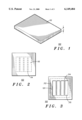
FIG. 1 is a perspective view of a layer of photosensitive glass used in a method for fabricating a field emission display in accordance with the present invention;
FIGS. 2 and 3 are top plan views of the layer of photosensitive glass of FIG. 1;
FIG. 4 is an exploded perspective view of a mechanical support/getter assembly in accordance with the present invention; and
FIG. 5 is an exploded perspective view of a field emission display including the mechanical support/getter assembly of FIG. 4 in accordance with the present invention.
It will be appreciated that for simplicity and clarity of illustration, elements shown in the FIGURES have not necessarily been drawn to scale. For example, the dimensions of some of the elements are exaggerated relative to each other. Further, where considered appropriate, reference numerals have been repeated among the FIGURES to indicate corresponding elements.
DESCRIPTION OF THE PREFERRED EMBODIMENTS
The invention is for a field emission display having a mechanical support/getter assembly, and for a method for fabricating the field emission display. The invention simplifies the fabrication of field emission displays. The method of the invention reduces the risk of harm to active elements of the display during the incorporation of spacer structures. It also provides ease of alignment of spacers. A field emission display in accordance with the invention has a gettering configuration that reduces the weight and volume of the display.
FIG. 1 illustrates a perspective view of a layer 100 of a photosensitive glass used in a method for fabricating a field emission display in accordance with the invention. Layer 100 has a thickness t. In the embodiment of FIG. 1, the thickness t is about 1 millimeter. In general, this photosensitive glass includes a glass that is crystallizable using a process that includes exposure to UV radiation, which is followed by a heat treatment. The heat treatment results in the crystallization of the photosensitive glass. The crystallized material is etchable upon exposure to an acid.
In the preferred embodiment, the photosensitive glass has the following composition: about 75 weight % SiO2, about 7 weight % LiO2, about 3 weight % K2 O, about 3 weight % Al2 O3, about 0.1 weight % Ag2 O, and about 0.02 weight % CcO2. This material may be obtained from Hoya Optical Division of Tokyo, Japan, which makes a photosensitive glass from their PEC3 glass. It may also be obtained from schott Glaswerke of Mainz, Germany, which makes a photosensitive glass from their "FOTURAN" glass.
FIG. 2 illustrates a top plan view of layer 100. Indicated in FIG. 2 by dashed-line boxes are a plurality of inter-spacer regions 110, which include generally rectangular regions of layer 100. In accordance with the method of the invention, inter-spacer regions 110 are removed. In the preferred embodiment, this removal is achieved by, first, selectively exposing inter-spacer regions 110 to ultraviolet radiation having a wavelength within the range of 280-320 nanometers. In the preferred embodiment, UV radiation at 320 nm is used. This UV exposure step is performed at room temperature.
Subsequent to the UV exposure, layer 100 is heated to a temperature of about 580° C. This heat treatment effects the crystallization of inter-spacer regions 110. The duration of this heat treatment depends upon the degree of crystallization desired. A higher degree of crystallization results in greater ease of etching with acid. By controlling the degree of crystallization, the etch rate during the subsequent acid treatment may be controlled. Inter-spacer regions 110 are removed completely, so that a high degree of crystallization therein is desired. This is achieved by performing the heating step for about one hour.
Following the selective crystallization of inter-spacer regions 110, the crystallized inter-spacer regions are removed by rinsing layer 100 with an acid solution. For the embodiment of FIG. 2, the acid solution includes an aqueous solution of hydrogen chloride, having 5-6 molar % hydrogen chloride. The acid solution is contacted equally with the opposing outer surfaces of the crystallized inter-spacer regions so that tapering along the depth of layer 100 is reduced.
Adjacent ones of inter-spacer regions 110 are spaced apart by about 100 micrometers. A spacer region 114 is disposed between adjacent inter-spacer reigons 110. Spacer regions 114 are not UV-exposed and, therefore, do not crystallize during the heating of layer 100. Thus, during the acid rinse, spacer regions 114 remain intact and glassy.
FIG. 3 illustrates a top plan view of layer 100 subsequent to the acid rinse step. The removal of inter-spacer regions 110 results in the formation of apertures 315 and a plurality of spacer ribs 314. Spacer ribs 314 are coextensive with a frame 312, which includes the portion of layer 100 that surrounds spacer ribs 314. In the embodiment of FIG. 3, each of spacer ribs 314 has a width of about 100 micrometers and a height of about 1 millimeter. These dimensions, as well as the length of spacer ribs 314, are predetermined to be compatible with the configuration of the field emission display. Further depicted in FIG. 3, by a dashed-line box and cross-hatching, is a getter frame region 120.
Following the formation of spacer ribs 314, the thickness of layer 100 is reduced at getter frame region 120 to form a getter land, which is described in greater detail with reference to FIG. 4. In one embodiment, the thickness of layer 100 is reduced at getter frame region 120 by etching getter frame region 120 in a manner similar to that described with respect to the removal of inter-spacer regions 110. Getter frame region 120 is selectively crystallized in a manner similar to that described with reference to FIG. 2. However, the extent of crystallization of getter frame region 120 is less than that of inter-spacer regions 110. This is achieved by one or both of the following modifications of the crystallization steps. First, the duration of the UV exposure can be reduced. Second, the duration and/or temperature of the heating step can be reduced.
After the selective crystallization of getter frame region 120, an acid etch similar to that described with reference to FIG. 2 is performed. The acid etch is controlled so that getter frame region 120 is partially removed to a predetermined depth that is less than the thickness of layer 100. In the embodiment of FIG. 3, the acid etch is performed at one of the opposed major surfaces of layer 100. The resulting structure comprises a unitary spacer/frame assembly, which is described in greater detail with respect to FIGS. 4 and 5.
In another embodiment of the invention, the step of reducing the thickness of layer 100 at getter frame region 120 includes performing a selective mechanical etch of getter frame region 120. The selective mechanical etch can be achieved by employing a precision sand blasting technique. This mechanical etch of getter frame region 120 is performed prior to the removal of inter-spacer regions 110.
FIG. 4 illustrates an exploded, perspective view of a mechanical support/getter assembly 300, in accordance with the invention. Mechanical support/getter assembly 300 includes a unitary spacer/frame assembly 310 and a getter frame 320. Unitary spacer/frame assembly 310 is made in the manner described with reference to FIGS. 1-3. The partial removal of getter frame region 120 of FIG. 3 forms a first peripheral portion 316 of frame 312. First peripheral portion 316 defines a getter land 322, as indicated in FIG. 4. Getter land 322 includes a surface upon which getter frame 320 is disposed. The region of frame 312 that is not etched includes a second peripheral portion 318, as indicated in FIG. 4.
Getter frame 320 is made from a gettering material, preferably powdered ZrO2, which is bonded to a substrate. The substrate may be made from nickel and has a thickness of about 50 micrometers. The scope of the invention is not limited to the particular gettering material of the preferred embodiment.
In the embodiment of FIG. 4, an outer peripheral portion 319 of frame 312 is partially etched to a predetermine depth, in a manner similar to that described with reference to the formation of getter land 322. The partial etch of outer peripheral portion 319 is performed at both of the opposed major surfaces of layer 100, so that a pair frit lands 323 are formed in outer peripheral portion 319.
FIG. 5 illustrates an exploded perspective view of a field emission display 400, in accordance with the invention. Field emission display 400 includes mechanical support/getter assembly 300 of FIG. 4. Field emission display 400 further includes a cathode plate 410 and an anode plate 430. Mechanical support/getter assembly 300 is disposed between an active major surface 420 of cathode plate 410 and an active major surface 440 of anode plate 430.
Active major surface 420 of cathode plate 410 includes electron emitting elements, such as Spindt tips, edge emitters, surface emitters, and the like. Active major surface 440 of anode plate 430 includes the electron-receiving elements, which are aligned with the electron emitting elements of cathode plate 410. These electron-receiving elements include deposits of cathode luminescent material.
Mechanical support/getter assembly 300 is affixed to cathode plate 410 and anode plate 430 by applying a frit sealant (not shown) to frit lands 323 and affixing cathode and anode plates 410, 430 thereto, as shown in FIG. 5. The application of the frit sealant to frit lands 323 reduces the display width that is attributable to the frit sealant.
The frit sealing process is performed in a vacuum oven. Sealing in a vacuum oven simultaneously establishes vacuum conditions in the compartments of field emission display 400. These compartments are defined by spacer ribs 314, active major surfaces 420, 440, frame 312, and getter frame 320. By performing the frit sealing step in a vacuum oven, evacuation of these compartments is not required subsequent to the frit sealing step.
In another embodiment of the present invention, the sum of the height of getter frame 320 and the height of first peripheral portion 316 is less than the height of second peripheral portion 318. This configuration defines gaps that allow fluid continuity between the compartments of the display. These gaps allow gases to flow around spacer ribs 314, so that the display compartments may be evacuated subsequent to the sealing step. Each of these gaps is defined by one of spacer ribs 314, second peripheral portion 318, active major surface 440, and getter frame 320.
Spacer ribs 314 provide standoff support between cathode plate 410 and anode plate 430 subsequent to the formation of the vacuum therebetween. Getter frame 320 removes contaminant gaseous species generated during the frit sealing process and during the operation of field emission display 400. Getter frame 320 is exposed to each of the compartments defined by spacer ribs 314. This ensures gettering action throughout field emission display 400.
In summary, a field emission display in accordance with the invention provides spacers which are simple to fabricate, handle, align, and affix. The present invention further provides a getter configuration and a frit sealing configuration which reduce the weight and volume of a field emission display.
While we have shown and described specific embodiments of the present invention, further modifications and improvements will occur to those skilled in the art. We desire it to be understood, therefore, that this invention is not limited to the particular forms shown and we intend in the appended claims to cover all modifications that do not depart from the spirit and scope of this invention.

Claims (10)

What is claimed is:
1. A method for fabricating a field emission display comprising the steps of:
providing a cathode plate having an active major surface;
providing an anode plate having an active major surface opposing the active major surface of the cathode plate;
providing a layer of a photosensitive glass having inter-spacer regions and a getter frame region and having a thickness;
selectively crystallizing the inter-spacer regions of the layer of the photosensitive glass, thereby forming crystallized inter-spacer regions;
reducing the thickness of the layer of the photosensitive glass at the getter frame region, thereby forming a getter land;
removing the crystallized inter-spacer regions, thereby forming a plurality of apertures and further realizing a unitary spacer/frame assembly;
providing a getter frame at the getter land, thereby forming a mechanical support/getter assembly having first and second opposed surfaces;
affixing the cathode plate to the first opposed surface of the mechanical support/getter assembly; and
affixing the anode plate to the second opposed surface of the mechanical support/getter assembly.
2. The method for fabricating a field emission display as claimed in claim 1, wherein the step of reducing the thickness of the layer of the photosensitive glass at the getter frame region comprises the steps of selectively crystallizing the getter frame region, thereby forming a crystallized getter frame region, and removing the crystallized getter frame region to a predetermined depth less than the thickness of the layer of the photosensitive glass.
3. The method for fabricating a field emission display as claimed in claim 2, wherein the step of selectively crystallizing the getter frame region comprises the steps of selectively exposing the getter frame region to UV radiation and thereafter heating the layer of the photosensitive glass to a temperature of about 580° C. for a duration sufficient to crystallize the getter frame region.
4. The method for fabricating a field emission display as claimed in claim 2, wherein the step of removing the crystallized getter frame region to a predetermined depth less that the thickness of the layer of the photosensitive glass comprises the step of contacting an acid with the layer of the photosensitive glass for a duration sufficient to remove the crystallized getter frame region to the predetermined depth.
5. The method for fabricating a field emission display as claimed in claim 1, wherein the step of reducing the thickness of the layer of the photosensitive glass at the getter frame region comprises the step of selectively sandblasting the getter frame region.
6. The method for fabricating a field emission display as claimed in claim 1, wherein the step of providing a layer of a photosensitive glass comprises the step of providing a layer made from about 75 weight % SiO2, about 7 weight % LiO2, about 3 weight % K2 O, about 3 weight % Al2 O3, about 0.1 weight % Ag2 O, and about 0.02 weight % CeO2.
7. The method for fabricating a field emission display as claimed in claim 1, wherein the step of removing the crystallized inter-spacer regions comprises the step of contacting an acid with the layer of the photosensitive glass for a duration sufficient to remove the crystallized inter-spacer regions to a depth equal to the thickness of the layer of the photosensitive glass.
8. The method for fabricating a field emission display as claimed in claim 1, wherein the step selectively crystallizing the inter-spacer regions comprises the steps of selectively exposing the inter-spacer regions to UV radiation and thereafter heating the layer of the photosensitive glass to a temperature of about 580° C. for a duration sufficient to crystallize the inter-spacer regions.
9. The method for fabricating a field emission display as claimed in claim 8, wherein the step of selectively exposing the inter-spacer regions to UV radiation comprises the step of selectively exposing the inter-spacer regions to radiation having a wavelength within a range of 280-320 nanometers.
10. A method for fabricating a field emission display comprising the steps of:
providing a cathode plate having an active major surface;
providing an anode plate having an active major surface opposing the active major surface of the cathode plate;
forming from a photosensitive glass a unitary spacer/frame assembly having a getter land;
providing a getter frame at the getter land, thereby forming a mechanical support/getter assembly having first and second opposed surfaces;
affixing the cathode plate to the first opposed surface of the mechanical support/getter assembly; and
affixing the anode plate to the second opposed surface of the mechanical support/getter assembly.
US09/092,922 1997-03-05 1998-06-05 Method of making field emission display having a mechanical support/getter assembly Expired - Fee Related US6149484A (en)

Priority Applications (1)

Application Number Priority Date Filing Date Title
US09/092,922 US6149484A (en) 1997-03-05 1998-06-05 Method of making field emission display having a mechanical support/getter assembly

Applications Claiming Priority (2)

Application Number Priority Date Filing Date Title
US08/811,653 US5894193A (en) 1997-03-05 1997-03-05 Field emission display with getter frame and spacer-frame assembly
US09/092,922 US6149484A (en) 1997-03-05 1998-06-05 Method of making field emission display having a mechanical support/getter assembly

Related Parent Applications (1)

Application Number Title Priority Date Filing Date
US08/811,653 Division US5894193A (en) 1997-03-05 1997-03-05 Field emission display with getter frame and spacer-frame assembly

Publications (1)

Publication Number Publication Date
US6149484A true US6149484A (en) 2000-11-21

Family

ID=25207164

Family Applications (2)

Application Number Title Priority Date Filing Date
US08/811,653 Expired - Lifetime US5894193A (en) 1997-03-05 1997-03-05 Field emission display with getter frame and spacer-frame assembly
US09/092,922 Expired - Fee Related US6149484A (en) 1997-03-05 1998-06-05 Method of making field emission display having a mechanical support/getter assembly

Family Applications Before (1)

Application Number Title Priority Date Filing Date
US08/811,653 Expired - Lifetime US5894193A (en) 1997-03-05 1997-03-05 Field emission display with getter frame and spacer-frame assembly

Country Status (7)

Country Link
US (2) US5894193A (en)
EP (1) EP0909455A1 (en)
JP (1) JP2000509899A (en)
KR (1) KR100337770B1 (en)
CN (1) CN1148775C (en)
TW (1) TW424257B (en)
WO (1) WO1998039788A1 (en)

Cited By (14)

* Cited by examiner, † Cited by third party
Publication number Priority date Publication date Assignee Title
US20020185964A1 (en) * 2001-06-08 2002-12-12 Sony Corporation Field emission display utilizing a cathode frame-type gate and anode with alignment method
US20020187707A1 (en) * 2001-06-08 2002-12-12 Sony Corporation And Sony Electronics Inc. Method for aligning field emission display components
US20020185950A1 (en) * 2001-06-08 2002-12-12 Sony Corporation And Sony Electronics Inc. Carbon cathode of a field emission display with in-laid isolation barrier and support
US20020185951A1 (en) * 2001-06-08 2002-12-12 Sony Corporation Carbon cathode of a field emission display with integrated isolation barrier and support on substrate
US20020195959A1 (en) * 2001-06-08 2002-12-26 Sony Corporation Method for driving a field emission display
US20030193296A1 (en) * 2002-04-16 2003-10-16 Sony Corporation Field emission display using line cathode structure
US20030193297A1 (en) * 2002-04-16 2003-10-16 Sony Corporation Field emission cathode structure using perforated gate
US20040007988A1 (en) * 2002-04-16 2004-01-15 Sony Corporation, A Japanese Corporation Field emission display with deflecting MEMS electrodes
US6682382B2 (en) * 2001-06-08 2004-01-27 Sony Corporation Method for making wires with a specific cross section for a field emission display
US20040100184A1 (en) * 2002-11-27 2004-05-27 Sony Corporation Spacer-less field emission display
US20040145299A1 (en) * 2003-01-24 2004-07-29 Sony Corporation Line patterned gate structure for a field emission display
US20040189552A1 (en) * 2003-03-31 2004-09-30 Sony Corporation Image display device incorporating driver circuits on active substrate to reduce interconnects
US20040189554A1 (en) * 2003-03-31 2004-09-30 Sony Corporation Image display device incorporating driver circuits on active substrate and other methods to reduce interconnects
US7277151B2 (en) 2001-10-15 2007-10-02 Samsung Sdi Co., Ltd. Flat panel display with photosensitive glass spacer

Families Citing this family (14)

* Cited by examiner, † Cited by third party
Publication number Priority date Publication date Assignee Title
IT1295366B1 (en) * 1997-10-20 1999-05-12 Getters Spa GETTER SYSTEM FOR PLASMA FLAT PANELS USED AS SCREENS
US6133689A (en) * 1997-12-31 2000-10-17 Micron Technology, Inc. Method and apparatus for spacing apart panels in flat panel displays
US6186849B1 (en) * 1998-03-24 2001-02-13 Saes Getters S.P.A. Process for the production of flat-screen grids coated with non-evaporable getter materials and grids thereby obtained
JP3706742B2 (en) * 1998-07-15 2005-10-19 パイオニア株式会社 Plasma display panel
US6137213A (en) * 1998-10-21 2000-10-24 Motorola, Inc. Field emission device having a vacuum bridge focusing structure and method
US6349908B1 (en) * 1999-02-17 2002-02-26 Eagle Electric Manufacturing Co., Inc. Standoff assembly and method for supporting an electrical component
US6307327B1 (en) * 2000-01-26 2001-10-23 Motorola, Inc. Method for controlling spacer visibility
US6888307B2 (en) * 2001-08-21 2005-05-03 Universal Display Corporation Patterned oxygen and moisture absorber for organic optoelectronic device structures
KR100446623B1 (en) * 2002-01-30 2004-09-04 삼성에스디아이 주식회사 Field emission display and manufacturing method thereof
KR100831005B1 (en) * 2002-02-27 2008-05-20 삼성에스디아이 주식회사 Spacer of field emission display and preparation method of the same
US20030115062A1 (en) * 2002-10-29 2003-06-19 Walker Marilyn A. Method for automated sentence planning
CN1328750C (en) * 2002-11-05 2007-07-25 鸿富锦精密工业(深圳)有限公司 Field emission display possessing sealing arrangement
KR100839410B1 (en) * 2002-11-26 2008-06-19 삼성에스디아이 주식회사 Method for fabricating spacer and flat panel display with the spacer
JP4863329B2 (en) 2004-01-26 2012-01-25 双葉電子工業株式会社 Fluorescent display tube

Citations (2)

* Cited by examiner, † Cited by third party
Publication number Priority date Publication date Assignee Title
US5520563A (en) * 1994-06-10 1996-05-28 Texas Instruments Incorporated Method of making a field emission device anode plate having an integrated getter
US5934964A (en) * 1994-02-28 1999-08-10 Saes Getters S.P.A. Field emitter flat display containing a getter and process for obtaining it

Family Cites Families (10)

* Cited by examiner, † Cited by third party
Publication number Priority date Publication date Assignee Title
US5223766A (en) * 1990-04-28 1993-06-29 Sony Corporation Image display device with cathode panel and gas absorbing getters
US5063323A (en) * 1990-07-16 1991-11-05 Hughes Aircraft Company Field emitter structure providing passageways for venting of outgassed materials from active electronic area
KR0139489B1 (en) * 1993-07-08 1998-06-01 호소야 레이지 Electric field radiate type display equipment
JP3241935B2 (en) * 1994-07-07 2001-12-25 富士通株式会社 Flat display device
US5629583A (en) * 1994-07-25 1997-05-13 Fed Corporation Flat panel display assembly comprising photoformed spacer structure, and method of making the same
FR2724041B1 (en) * 1994-08-24 1997-04-11 Pixel Int Sa INTER-ELECTRODES HIGH VOLTAGE DISPLAY FLAT SCREEN
JP3402780B2 (en) * 1994-09-02 2003-05-06 キヤノン株式会社 Image display device
US5503582A (en) * 1994-11-18 1996-04-02 Micron Display Technology, Inc. Method for forming spacers for display devices employing reduced pressures
JP3423519B2 (en) * 1996-01-19 2003-07-07 キヤノン株式会社 Image forming device
US5708325A (en) * 1996-05-20 1998-01-13 Motorola Display spacer structure for a field emission device

Patent Citations (2)

* Cited by examiner, † Cited by third party
Publication number Priority date Publication date Assignee Title
US5934964A (en) * 1994-02-28 1999-08-10 Saes Getters S.P.A. Field emitter flat display containing a getter and process for obtaining it
US5520563A (en) * 1994-06-10 1996-05-28 Texas Instruments Incorporated Method of making a field emission device anode plate having an integrated getter

Cited By (30)

* Cited by examiner, † Cited by third party
Publication number Priority date Publication date Assignee Title
US6663454B2 (en) 2001-06-08 2003-12-16 Sony Corporation Method for aligning field emission display components
US20020185950A1 (en) * 2001-06-08 2002-12-12 Sony Corporation And Sony Electronics Inc. Carbon cathode of a field emission display with in-laid isolation barrier and support
US7118439B2 (en) 2001-06-08 2006-10-10 Sony Corporation Field emission display utilizing a cathode frame-type gate and anode with alignment method
US6682382B2 (en) * 2001-06-08 2004-01-27 Sony Corporation Method for making wires with a specific cross section for a field emission display
US20020195959A1 (en) * 2001-06-08 2002-12-26 Sony Corporation Method for driving a field emission display
US6624590B2 (en) 2001-06-08 2003-09-23 Sony Corporation Method for driving a field emission display
US6885145B2 (en) 2001-06-08 2005-04-26 Sony Corporation Field emission display using gate wires
US20020185964A1 (en) * 2001-06-08 2002-12-12 Sony Corporation Field emission display utilizing a cathode frame-type gate and anode with alignment method
US20050179397A1 (en) * 2001-06-08 2005-08-18 Sony Corporation Field emission display utilizing a cathode frame-type gate and anode with alignment method
US20020187707A1 (en) * 2001-06-08 2002-12-12 Sony Corporation And Sony Electronics Inc. Method for aligning field emission display components
US20020185951A1 (en) * 2001-06-08 2002-12-12 Sony Corporation Carbon cathode of a field emission display with integrated isolation barrier and support on substrate
US20040090163A1 (en) * 2001-06-08 2004-05-13 Sony Corporation Field emission display utilizing a cathode frame-type gate
US7002290B2 (en) 2001-06-08 2006-02-21 Sony Corporation Carbon cathode of a field emission display with integrated isolation barrier and support on substrate
US20040104667A1 (en) * 2001-06-08 2004-06-03 Sony Corporation Field emission display using gate wires
US6989631B2 (en) 2001-06-08 2006-01-24 Sony Corporation Carbon cathode of a field emission display with in-laid isolation barrier and support
US6756730B2 (en) 2001-06-08 2004-06-29 Sony Corporation Field emission display utilizing a cathode frame-type gate and anode with alignment method
US6940219B2 (en) 2001-06-08 2005-09-06 Sony Corporation Field emission display utilizing a cathode frame-type gate
US7277151B2 (en) 2001-10-15 2007-10-02 Samsung Sdi Co., Ltd. Flat panel display with photosensitive glass spacer
US20030193297A1 (en) * 2002-04-16 2003-10-16 Sony Corporation Field emission cathode structure using perforated gate
US6873118B2 (en) 2002-04-16 2005-03-29 Sony Corporation Field emission cathode structure using perforated gate
US6791278B2 (en) * 2002-04-16 2004-09-14 Sony Corporation Field emission display using line cathode structure
US6747416B2 (en) 2002-04-16 2004-06-08 Sony Corporation Field emission display with deflecting MEMS electrodes
US20040007988A1 (en) * 2002-04-16 2004-01-15 Sony Corporation, A Japanese Corporation Field emission display with deflecting MEMS electrodes
US20030193296A1 (en) * 2002-04-16 2003-10-16 Sony Corporation Field emission display using line cathode structure
US20040100184A1 (en) * 2002-11-27 2004-05-27 Sony Corporation Spacer-less field emission display
US7012582B2 (en) 2002-11-27 2006-03-14 Sony Corporation Spacer-less field emission display
US20040145299A1 (en) * 2003-01-24 2004-07-29 Sony Corporation Line patterned gate structure for a field emission display
US20040189554A1 (en) * 2003-03-31 2004-09-30 Sony Corporation Image display device incorporating driver circuits on active substrate and other methods to reduce interconnects
US20040189552A1 (en) * 2003-03-31 2004-09-30 Sony Corporation Image display device incorporating driver circuits on active substrate to reduce interconnects
US7071629B2 (en) 2003-03-31 2006-07-04 Sony Corporation Image display device incorporating driver circuits on active substrate and other methods to reduce interconnects

Also Published As

Publication number Publication date
CN1216147A (en) 1999-05-05
KR20000065199A (en) 2000-11-06
EP0909455A4 (en) 1999-05-12
WO1998039788A1 (en) 1998-09-11
KR100337770B1 (en) 2002-07-18
US5894193A (en) 1999-04-13
CN1148775C (en) 2004-05-05
TW424257B (en) 2001-03-01
EP0909455A1 (en) 1999-04-21
JP2000509899A (en) 2000-08-02

Similar Documents

Publication Publication Date Title
US6149484A (en) Method of making field emission display having a mechanical support/getter assembly
US5980346A (en) Method for fabricating a display spacer assembly
US5717287A (en) Spacers for a flat panel display and method
US20060232186A1 (en) Spacers for field emission displays
US5731660A (en) Flat panel display spacer structure
US6140762A (en) Wall assembly and method for attaching walls for flat panel displays
JP3270054B2 (en) Field emission device with internal structure for aligning phosphor pixels with corresponding field emitters
KR100555835B1 (en) Method for fabricating a flat panel device
JP3347648B2 (en) Display device
US20050127563A1 (en) Method of manufacturing spacer assembly, filling method for spacer forming material, filling device for spacer forming material, molding tool, and vacuum vessel
KR100258799B1 (en) Method of fabricating spacer of fed
KR100315234B1 (en) Flat panel display device
KR100374044B1 (en) The making method of FED's spacer electrode
KR19990043897A (en) Flat Panel Display and Forming Method
KR100542182B1 (en) Flat panel display device
US20050231088A1 (en) Mesh structure of tetraode field-emission display and method of fabricating the same
KR100300335B1 (en) A method of manufacturing for a flat panel display
US20050231089A1 (en) Mesh structure of tetraode field-emission display and method of fabricating the same
JPS581956A (en) Flat display unit of electron beam accelerating type
KR100403081B1 (en) Cell and spacer of structure of feild display
KR20020057328A (en) The FED equipped T-type spacer and the manufacturing method
JPH10199451A (en) Panel structure of display device
JP2001052633A (en) Flat-plate display device with high aspect ratio spacer and manufacture of display device
KR970003355A (en) Structure and manufacturing method of field emission display device
JPS6222362A (en) Vacuum case

Legal Events

Date Code Title Description
FPAY Fee payment

Year of fee payment: 4

FPAY Fee payment

Year of fee payment: 8

AS Assignment

Owner name: MOTOROLA, INC., ILLINOIS

Free format text: ASSIGNMENT OF ASSIGNORS INTEREST;ASSIGNORS:AMRINE, CRAIG;ANDERSON, CLIFFORD L.;PETERSEN, RONALD O.;REEL/FRAME:026369/0415

Effective date: 19970312

AS Assignment

Owner name: MOTOROLA SOLUTIONS, INC., ILLINOIS

Free format text: CHANGE OF NAME;ASSIGNOR:MOTOROLA, INC;REEL/FRAME:026382/0087

Effective date: 20110104

REMI Maintenance fee reminder mailed
LAPS Lapse for failure to pay maintenance fees
STCH Information on status: patent discontinuation

Free format text: PATENT EXPIRED DUE TO NONPAYMENT OF MAINTENANCE FEES UNDER 37 CFR 1.362

FP Expired due to failure to pay maintenance fee

Effective date: 20121121