US6150220A - Insulation layer structure and method for making the same - Google Patents
Insulation layer structure and method for making the same Download PDFInfo
- Publication number
- US6150220A US6150220A US09/195,550 US19555098A US6150220A US 6150220 A US6150220 A US 6150220A US 19555098 A US19555098 A US 19555098A US 6150220 A US6150220 A US 6150220A
- Authority
- US
- United States
- Prior art keywords
- layer
- impurity
- pad
- insulation layer
- insulation
- Prior art date
- Legal status (The legal status is an assumption and is not a legal conclusion. Google has not performed a legal analysis and makes no representation as to the accuracy of the status listed.)
- Expired - Lifetime
Links
Images

Classifications
-
- H—ELECTRICITY
- H01—ELECTRIC ELEMENTS
- H01L—SEMICONDUCTOR DEVICES NOT COVERED BY CLASS H10
- H01L21/00—Processes or apparatus adapted for the manufacture or treatment of semiconductor or solid state devices or of parts thereof
- H01L21/02—Manufacture or treatment of semiconductor devices or of parts thereof
- H01L21/04—Manufacture or treatment of semiconductor devices or of parts thereof the devices having at least one potential-jump barrier or surface barrier, e.g. PN junction, depletion layer or carrier concentration layer
- H01L21/18—Manufacture or treatment of semiconductor devices or of parts thereof the devices having at least one potential-jump barrier or surface barrier, e.g. PN junction, depletion layer or carrier concentration layer the devices having semiconductor bodies comprising elements of Group IV of the Periodic System or AIIIBV compounds with or without impurities, e.g. doping materials
-
- H—ELECTRICITY
- H01—ELECTRIC ELEMENTS
- H01L—SEMICONDUCTOR DEVICES NOT COVERED BY CLASS H10
- H01L21/00—Processes or apparatus adapted for the manufacture or treatment of semiconductor or solid state devices or of parts thereof
- H01L21/70—Manufacture or treatment of devices consisting of a plurality of solid state components formed in or on a common substrate or of parts thereof; Manufacture of integrated circuit devices or of parts thereof
- H01L21/77—Manufacture or treatment of devices consisting of a plurality of solid state components or integrated circuits formed in, or on, a common substrate
- H01L21/78—Manufacture or treatment of devices consisting of a plurality of solid state components or integrated circuits formed in, or on, a common substrate with subsequent division of the substrate into plural individual devices
- H01L21/82—Manufacture or treatment of devices consisting of a plurality of solid state components or integrated circuits formed in, or on, a common substrate with subsequent division of the substrate into plural individual devices to produce devices, e.g. integrated circuits, each consisting of a plurality of components
- H01L21/822—Manufacture or treatment of devices consisting of a plurality of solid state components or integrated circuits formed in, or on, a common substrate with subsequent division of the substrate into plural individual devices to produce devices, e.g. integrated circuits, each consisting of a plurality of components the substrate being a semiconductor, using silicon technology
- H01L21/8232—Field-effect technology
- H01L21/8234—MIS technology, i.e. integration processes of field effect transistors of the conductor-insulator-semiconductor type
- H01L21/823462—MIS technology, i.e. integration processes of field effect transistors of the conductor-insulator-semiconductor type with a particular manufacturing method of the gate insulating layers, e.g. different gate insulating layer thicknesses, particular gate insulator materials or particular gate insulator implants
-
- Y—GENERAL TAGGING OF NEW TECHNOLOGICAL DEVELOPMENTS; GENERAL TAGGING OF CROSS-SECTIONAL TECHNOLOGIES SPANNING OVER SEVERAL SECTIONS OF THE IPC; TECHNICAL SUBJECTS COVERED BY FORMER USPC CROSS-REFERENCE ART COLLECTIONS [XRACs] AND DIGESTS
- Y10—TECHNICAL SUBJECTS COVERED BY FORMER USPC
- Y10S—TECHNICAL SUBJECTS COVERED BY FORMER USPC CROSS-REFERENCE ART COLLECTIONS [XRACs] AND DIGESTS
- Y10S148/00—Metal treatment
- Y10S148/043—Dual dielectric
-
- Y—GENERAL TAGGING OF NEW TECHNOLOGICAL DEVELOPMENTS; GENERAL TAGGING OF CROSS-SECTIONAL TECHNOLOGIES SPANNING OVER SEVERAL SECTIONS OF THE IPC; TECHNICAL SUBJECTS COVERED BY FORMER USPC CROSS-REFERENCE ART COLLECTIONS [XRACs] AND DIGESTS
- Y10—TECHNICAL SUBJECTS COVERED BY FORMER USPC
- Y10S—TECHNICAL SUBJECTS COVERED BY FORMER USPC CROSS-REFERENCE ART COLLECTIONS [XRACs] AND DIGESTS
- Y10S148/00—Metal treatment
- Y10S148/163—Thick-thin oxides
-
- Y—GENERAL TAGGING OF NEW TECHNOLOGICAL DEVELOPMENTS; GENERAL TAGGING OF CROSS-SECTIONAL TECHNOLOGIES SPANNING OVER SEVERAL SECTIONS OF THE IPC; TECHNICAL SUBJECTS COVERED BY FORMER USPC CROSS-REFERENCE ART COLLECTIONS [XRACs] AND DIGESTS
- Y10—TECHNICAL SUBJECTS COVERED BY FORMER USPC
- Y10S—TECHNICAL SUBJECTS COVERED BY FORMER USPC CROSS-REFERENCE ART COLLECTIONS [XRACs] AND DIGESTS
- Y10S438/00—Semiconductor device manufacturing: process
- Y10S438/981—Utilizing varying dielectric thickness
Definitions
- the present invention relates to a semiconductor device and a fabrication method thereof and more particularly, to an insulation layer structure and a method of making the insulation layer structure for a semiconductor device.
- an ion implanting method or an etching method is used.
- the ion implanting methods use either nitrogen or fluorine.
- the nitrogen ion implanting method is used to form a relatively thin gate insulation layer, while the fluorine ion implanting method is employed to form a relatively thick gate insulation layer.
- gate insulation layers formed by nitrogen ion implanting tend to have a relatively poor reliability, while gate insulation layers formed by fluorine ion implanting may exhibit increased junction leakage current since fluorine defects are formed around junctions of fluorine ion implanted gate insulation layers.
- a dual thickness insulation layer may be formed using a dry etching technique or a wet etching technique.
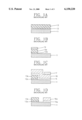
- FIGS. 1A through 1D are cross-sectional views sequentially illustrating process steps in the formation of a background dual thickness insulation layer, for a semiconductor device, using a dry etching method.
- a first insulation layer 12 is formed on a semiconductor substrate 11.
- a first gate electrode layer 13 is formed on the first insulation layer 12.
- a first photoresist pattern 14 is then formed on the first gate electrode layer 13. See FIG. 1B.
- the first photoresist pattern 14 as a mask in a dry etching method, the first gate electrode layer 13 and the first insulation layer 12 are sequentially removed to form a first gate electrode layer pattern 13a and a first gate insulation layer pattern 12a.
- a second insulation layer 15 is formed on the semiconductor substrate 11, the first gate electrode layer pattern 13a, and the first gate insulation layer pattern 12a.
- the second insulation layer 15 is formed thicker (or thinner) than the first insulation layer 12 such that the first insulation layer 12 and the second insulation layer 15 have different thicknesses.
- a second gate electrode layer 16 is formed on the second insulation layer 15.
- a second photoresist pattern 17 is formed on the second gate electrode layer 16.
- the second gate electrode layer 16 and the second insulation layer 15 are sequentially removed, by a dry etching method, to form a second gate electrode layer pattern 16a and a second gate insulation layer pattern 15a. Thereafter, the second photoresist pattern 17 is removed.
- FIGS. 1A-1D The method of FIGS. 1A-1D is disadvantageous since formation of the first and second insulation layers having different thicknesses using a dry etching process requires highly complicated fabrication steps. Further, when the first gate electrode layer pattern 13a needs to be doped by ion implanting, the first gate electrode layer pattern 13a absorbs more heat than does the second gate electrode layer pattern 15a, resulting in decreased product reliability. Furthermore, use of a dry etching method for the formation of the dual thickness insulation layer may result in a damaged semiconductor device.
- FIGS. 2A through 2C are cross-sectional views sequentially illustrating process steps in a background method of forming a dual thickness insulation layer for a semiconductor device using a wet etching method.
- a first oxide layer 23 serving as an insulation layer is formed on a semiconductor substrate 21.
- a first photoresist pattern 25 is formed on the first insulation layer 23.
- the first oxide layer 23 is etched using a wet etching method, and the first photoresist pattern 25 is removed.
- a second oxide layer 27 is grown on the first oxide layer 23 and the exposed semiconductor substrate 21.
- the method of FIGS. 2A-2C is disadvantageous due to numerous repetitions of the growing step and the etching step which may be needed to form the dual thickness insulation layer and it may be difficult to form the required thickness of the insulation layer.
- the gate insulation layer may be subject to damage when removing the photoresist pattern.
- the gate insulation layer should be grown twice for its formation, thereby deteriorating the product reliability.
- An object of the present invention is to solve at least one of the problems and disadvantages of the background art and/or prior art.
- Another object of the present invention is to simplify the gate insulation layer fabricating steps.
- Another object is to provide an improved reproducibility and product reliability of the gate insulation layer.
- a method for fabricating an insulation layer for a semiconductor device including the steps of: preparing a semiconductor substrate; forming an impurity layer in the semiconductor substrate, the impurity layer including a first portion of the impurity layer and a second portion of the impurity layer; and growing an insulation layer in the semiconductor substrate, the insulation layer including a first portion of the insulation layer and a second portion of the insulation layer, wherein the first portion and the second portion of the insulation layer differ from each other in thickness.
- an insulation layer structure for a semiconductor device wherein the insolation layer structure includes: a first insulation layer formed on a semiconductor substrate, the first insulation layer being irregular, or varying, in thickness; a second insulation layer formed on the first insulation layer, the second insulation layer varying in thickness depending on the thickness of the underlying first insulation layer.
- FIGS. 1A through 1D are cross-sectional views sequentially illustrating steps in a background dual process for formation of a thickness insulation layer for a semiconductor device using a dry etching method, according to the prior art;
- FIGS. 2A through 2C are cross-sectional views sequentially illustrating steps in a background process for formation of a dual thickness insulation layer for a semiconductor device using a wet etching method
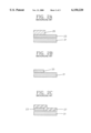
- FIGS. 3A through 3D are cross-sectional views illustrating steps in a method for fabricating a dual thickness gate insulation layer according to a preferred embodiment of the present invention.
- FIGS. 3A through 3D are cross-sectional views illustrating steps in a method for fabricating a dual thickness gate insulation layer for a semiconductor device according to a preferred embodiment of the present invention.
- a pad layer 33 is formed on a semiconductor substrate 31.
- a photoresist pattern 35 is formed on the pad layer 33.
- the photoresist pattern 35 serves as a mask for defining a thick portion 39a and a thin portion 39b of an insulation layer 39 which is to be formed in a later step (FIG. 3D).
- the pad layer 33 is etched using a wet etching technique. At this time, the pad layer 33 is not completely etched in order to prevent damage from occurring to the semiconductor substrate 31 which lies beneath the etching target, normally, the pad layer 33.
- the pad layer 33 comprises a first portion 33a and a second portion 33b which have different thicknesses. In the particular instance shown in FIG. 3B, the first portion 33a of the pad layer 33 is thicker than the second portion 33b of the pad layer 33.
- the photoresist pattern 35 is removed, and the pad layer 33 is cleaned. Subsequently, the semiconductor substrate 31 and the pad layer 33 are annealed under an atmosphere of nitrous gas, such as N 2 O and NO. Under such an annealing process, a nitrous impurity layer (or "ion layer”) 37 is formed in the semiconductor substrate 31.
- the nitrous impurity layer 37 comprises a first region 37a and a second region 37b which differ from each other in the amount of impurity contained therein.
- the first region 37a of the nitrous impurity layer 37 which comprises a lesser amount of impurity as compared with the second region 37b, is formed just beneath the first portion 33a of the pad layer 33.
- the second region 37b of the nitrous impurity layer 37 which comprises a larger amount of impurity as compared with the first region 37a, is formed just beneath the second portion 33b of the pad layer 33.
- the first region 37a of the impurity layer 37 is thinner than the second region 37b.
- the insulation layer 39 comprises a first portion 39a and a second portion 39b which are different in thickness.
- the first portion 39a of the first insulation layer 39 is thicker than the second portion 39b of the first insulation layer 39.
- the nitrous impurity layer 37 serves to delay or inhibit the growth of the insulation layer 39. Differences in the relative amount of impurity in the first region 37a as compared with the second region 37b of the nitrous impurity layer 37 allows the relatively thick first portion 39a of the insulation layer 39 to be formed just beneath the first region 37a of the nitrous impurity layer 37, and the relatively thin second portion 39b of the insulation layer 39 to be formed just beneath the second region 37b of the nitrous impurity layer 37. If the insulation layer 39 serves as a first insulation layer in FIG. 3D, the impurity layer 37 formed on the first insulation layer 39 serves as a second insulation layer.
- a method for forming an insulation layer for a semiconductor device provides an improved reproducibility of the insulation layer thickness. Because the second insulation layer in the form of an impurity layer exists on the first insulation layer, other impurities are prevented from being implanted, while providing enhanced reliability of the insulation layer. Further, the dual thickness insulation layer of the preferred embodiment is formed in a single growth step, thereby greatly simplifying the process steps and accordingly decreasing the production cost.
Abstract
Description
Claims (26)
Applications Claiming Priority (2)
| Application Number | Priority Date | Filing Date | Title |
|---|---|---|---|
| KR98-6379 | 1998-02-27 | ||
| KR1019980006379A KR100273281B1 (en) | 1998-02-27 | 1998-02-27 | Method of forming insulator film of semiconductor device |
Publications (1)
| Publication Number | Publication Date |
|---|---|
| US6150220A true US6150220A (en) | 2000-11-21 |
Family
ID=19533912
Family Applications (1)
| Application Number | Title | Priority Date | Filing Date |
|---|---|---|---|
| US09/195,550 Expired - Lifetime US6150220A (en) | 1998-02-27 | 1998-11-19 | Insulation layer structure and method for making the same |
Country Status (5)
| Country | Link |
|---|---|
| US (1) | US6150220A (en) |
| JP (1) | JPH11289090A (en) |
| KR (1) | KR100273281B1 (en) |
| DE (1) | DE19839079C2 (en) |
| TW (1) | TW392246B (en) |
Cited By (8)
| Publication number | Priority date | Publication date | Assignee | Title |
|---|---|---|---|---|
| US6225163B1 (en) * | 2000-02-18 | 2001-05-01 | National Semiconductor Corporation | Process for forming high quality gate silicon dioxide layers of multiple thicknesses |
| US6261972B1 (en) * | 2000-11-06 | 2001-07-17 | Infineon Technologies Ag | Dual gate oxide process for uniform oxide thickness |
| US6358865B2 (en) * | 1999-05-14 | 2002-03-19 | Agere Systems Guardian Corp. | Oxidation of silicon using fluorine implant |
| WO2003005411A2 (en) * | 2001-07-02 | 2003-01-16 | Infineon Technologies Ag | Method for producing a stepped structure on a substrate |
| US6541393B2 (en) | 2000-02-29 | 2003-04-01 | Fujitsu Limited | Method for fabricating semiconductor device |
| US20040150067A1 (en) * | 2002-11-12 | 2004-08-05 | Bruno Ghyselen | Semiconductor structure and methods for fabricating same |
| CN102479712A (en) * | 2010-11-29 | 2012-05-30 | 无锡华润上华半导体有限公司 | Dual gate oxide semiconductor device manufacturing method |
| US10845627B2 (en) * | 2017-10-11 | 2020-11-24 | Samsung Electronics Co., Ltd. | Meta device and manufacturing method thereof |
Families Citing this family (7)
| Publication number | Priority date | Publication date | Assignee | Title |
|---|---|---|---|---|
| JP2008277836A (en) * | 1999-04-26 | 2008-11-13 | Renesas Technology Corp | Semiconductor integrated circuit device |
| KR100408001B1 (en) * | 2001-12-28 | 2003-12-01 | 주식회사 하이닉스반도체 | Method for forming gate isolation film of semiconductor |
| DE10207122B4 (en) * | 2002-02-20 | 2007-07-05 | Advanced Micro Devices, Inc., Sunnyvale | A method of forming layers of oxide on a surface of a substrate |
| KR100466209B1 (en) * | 2002-07-08 | 2005-01-13 | 매그나칩 반도체 유한회사 | Method of manufacturing semiconductor device |
| KR100602109B1 (en) * | 2002-07-30 | 2006-07-19 | 동부일렉트로닉스 주식회사 | Method for forming gate oxide layer of semiconductor device |
| KR100470942B1 (en) * | 2003-06-27 | 2005-03-14 | 주식회사 하이닉스반도체 | Method for forming tunnel oxide in a semiconductor device |
| KR100611784B1 (en) * | 2004-12-29 | 2006-08-10 | 주식회사 하이닉스반도체 | Semiconductor device with multi-gate dielectric and method for manufacturing the same |
Citations (6)
| Publication number | Priority date | Publication date | Assignee | Title |
|---|---|---|---|---|
| US4151010A (en) * | 1978-06-30 | 1979-04-24 | International Business Machines Corporation | Forming adjacent impurity regions in a semiconductor by oxide masking |
| US4651406A (en) * | 1980-02-27 | 1987-03-24 | Hitachi, Ltd. | Forming memory transistors with varying gate oxide thicknesses |
| US4851370A (en) * | 1987-12-28 | 1989-07-25 | American Telephone And Telegraph Company, At&T Bell Laboratories | Fabricating a semiconductor device with low defect density oxide |
| US5360769A (en) * | 1992-12-17 | 1994-11-01 | Micron Semiconductor, Inc. | Method for fabricating hybrid oxides for thinner gate devices |
| US5497021A (en) * | 1992-04-30 | 1996-03-05 | Fuji Electric Co., Ltd. | CMOS structure with varying gate oxide thickness and with both different and like conductivity-type gate electrodes |
| US5881085A (en) * | 1996-07-25 | 1999-03-09 | Picolight, Incorporated | Lens comprising at least one oxidized layer and method for forming same |
Family Cites Families (7)
| Publication number | Priority date | Publication date | Assignee | Title |
|---|---|---|---|---|
| JPS5637635A (en) * | 1979-09-05 | 1981-04-11 | Mitsubishi Electric Corp | Manufacture of semiconductor device |
| JPS5854638A (en) * | 1981-09-28 | 1983-03-31 | Mitsubishi Electric Corp | Manufacture of semiconductor device |
| JPS60201636A (en) * | 1984-03-27 | 1985-10-12 | Fujitsu Ltd | Manufacture of semiconductor device |
| JP3102223B2 (en) * | 1993-09-24 | 2000-10-23 | 住友金属工業株式会社 | Oxidation method of silicon substrate |
| KR0136935B1 (en) * | 1994-04-21 | 1998-04-24 | 문정환 | Method of manufacturing memory device |
| US5672521A (en) * | 1995-11-21 | 1997-09-30 | Advanced Micro Devices, Inc. | Method of forming multiple gate oxide thicknesses on a wafer substrate |
| US5882993A (en) * | 1996-08-19 | 1999-03-16 | Advanced Micro Devices, Inc. | Integrated circuit with differing gate oxide thickness and process for making same |
-
1998
- 1998-02-27 KR KR1019980006379A patent/KR100273281B1/en not_active IP Right Cessation
- 1998-07-17 TW TW087111700A patent/TW392246B/en not_active IP Right Cessation
- 1998-08-27 DE DE19839079A patent/DE19839079C2/en not_active Expired - Fee Related
- 1998-11-19 US US09/195,550 patent/US6150220A/en not_active Expired - Lifetime
-
1999
- 1999-02-24 JP JP11045721A patent/JPH11289090A/en active Pending
Patent Citations (6)
| Publication number | Priority date | Publication date | Assignee | Title |
|---|---|---|---|---|
| US4151010A (en) * | 1978-06-30 | 1979-04-24 | International Business Machines Corporation | Forming adjacent impurity regions in a semiconductor by oxide masking |
| US4651406A (en) * | 1980-02-27 | 1987-03-24 | Hitachi, Ltd. | Forming memory transistors with varying gate oxide thicknesses |
| US4851370A (en) * | 1987-12-28 | 1989-07-25 | American Telephone And Telegraph Company, At&T Bell Laboratories | Fabricating a semiconductor device with low defect density oxide |
| US5497021A (en) * | 1992-04-30 | 1996-03-05 | Fuji Electric Co., Ltd. | CMOS structure with varying gate oxide thickness and with both different and like conductivity-type gate electrodes |
| US5360769A (en) * | 1992-12-17 | 1994-11-01 | Micron Semiconductor, Inc. | Method for fabricating hybrid oxides for thinner gate devices |
| US5881085A (en) * | 1996-07-25 | 1999-03-09 | Picolight, Incorporated | Lens comprising at least one oxidized layer and method for forming same |
Cited By (15)
| Publication number | Priority date | Publication date | Assignee | Title |
|---|---|---|---|---|
| US6358865B2 (en) * | 1999-05-14 | 2002-03-19 | Agere Systems Guardian Corp. | Oxidation of silicon using fluorine implant |
| US6225163B1 (en) * | 2000-02-18 | 2001-05-01 | National Semiconductor Corporation | Process for forming high quality gate silicon dioxide layers of multiple thicknesses |
| US6541393B2 (en) | 2000-02-29 | 2003-04-01 | Fujitsu Limited | Method for fabricating semiconductor device |
| US6261972B1 (en) * | 2000-11-06 | 2001-07-17 | Infineon Technologies Ag | Dual gate oxide process for uniform oxide thickness |
| WO2003005411A3 (en) * | 2001-07-02 | 2003-09-18 | Infineon Technologies Ag | Method for producing a stepped structure on a substrate |
| DE10131917A1 (en) * | 2001-07-02 | 2003-01-23 | Infineon Technologies Ag | Method for producing a step-like structure on a substrate |
| WO2003005411A2 (en) * | 2001-07-02 | 2003-01-16 | Infineon Technologies Ag | Method for producing a stepped structure on a substrate |
| US20040185646A1 (en) * | 2001-07-02 | 2004-09-23 | Infineon Technologies Ag | Method for creating a stepped structure on a substrate |
| US6946339B2 (en) * | 2001-07-02 | 2005-09-20 | Infineon Technologies Ag | Method for creating a stepped structure on a substrate |
| US20040150067A1 (en) * | 2002-11-12 | 2004-08-05 | Bruno Ghyselen | Semiconductor structure and methods for fabricating same |
| US6955971B2 (en) * | 2002-11-12 | 2005-10-18 | S.O.I.Tec Silicon On Insulator Technologies S.A. | Semiconductor structure and methods for fabricating same |
| DE10393700B4 (en) | 2002-11-12 | 2019-06-06 | Soitec | A method of manufacturing a semiconductor device by forming weakened regions or a weakened layer and associated semiconductor device |
| CN102479712A (en) * | 2010-11-29 | 2012-05-30 | 无锡华润上华半导体有限公司 | Dual gate oxide semiconductor device manufacturing method |
| US10845627B2 (en) * | 2017-10-11 | 2020-11-24 | Samsung Electronics Co., Ltd. | Meta device and manufacturing method thereof |
| US11668962B2 (en) | 2017-10-11 | 2023-06-06 | Samsung Electronics Co., Ltd. | Meta device and manufacturing method thereof |
Also Published As
| Publication number | Publication date |
|---|---|
| KR19990071115A (en) | 1999-09-15 |
| KR100273281B1 (en) | 2000-12-15 |
| TW392246B (en) | 2000-06-01 |
| DE19839079C2 (en) | 2002-08-01 |
| JPH11289090A (en) | 1999-10-19 |
| DE19839079A1 (en) | 1999-09-09 |
Similar Documents
| Publication | Publication Date | Title |
|---|---|---|
| US6150220A (en) | Insulation layer structure and method for making the same | |
| US5747373A (en) | Nitride-oxide sidewall spacer for salicide formation | |
| US5073514A (en) | Method of manufacturing mis semiconductor device | |
| US7449392B2 (en) | Semiconductor device capable of threshold voltage adjustment by applying an external voltage | |
| JPS6010773A (en) | Method of forming 1-element fet-memory capacitor circuit | |
| US6294434B1 (en) | Method of forming a metal silicide layer on a polysilicon gate structure and on a source/drain region of a MOSFET device | |
| US5637529A (en) | Method for forming element isolation insulating film of semiconductor device | |
| US6927110B2 (en) | Method of manufacturing a semiconductor device | |
| US5972777A (en) | Method of forming isolation by nitrogen implant to reduce bird's beak | |
| US6146972A (en) | Method for fabricating semiconductor device | |
| US6524910B1 (en) | Method of forming dual thickness gate dielectric structures via use of silicon nitride layers | |
| KR100223736B1 (en) | Method of manufacturing semiconductor device | |
| US5744391A (en) | Method to improve isolation between EEPROM devices via a field oxide anneal | |
| US6221745B1 (en) | High selectivity mask oxide etching to suppress silicon pits | |
| JPH07176742A (en) | Manufacture of semiconductor device and semiconductor device | |
| JPH03227024A (en) | Manufacture of semiconductor device | |
| JPS63275181A (en) | Manufacture of semiconductor device | |
| JPS6021540A (en) | Manufacture of semiconductor device | |
| US6818495B1 (en) | Method for forming high purity silicon oxide field oxide isolation region | |
| EP0482829A1 (en) | Method for forming a composite oxide over a heavily doped region | |
| JPS58162064A (en) | Manufacture of semiconductor device | |
| KR0167260B1 (en) | Manufacture of semiconductor device | |
| JPH0286135A (en) | Manufacture of semiconductor device | |
| JPH01238026A (en) | Manufacture of semiconductor device | |
| JPS6188543A (en) | Manufacture of semiconductor device |
Legal Events
| Date | Code | Title | Description |
|---|---|---|---|
| AS | Assignment |
Owner name: LG SEMICON CO., LTD., KOREA, REPUBLIC OF Free format text: ASSIGNMENT OF ASSIGNORS INTEREST;ASSIGNORS:HUH, YUN-JUN;CHO, NAM-HOON;REEL/FRAME:009597/0149 Effective date: 19981103 |
|
| AS | Assignment |
Owner name: HYUNDAI ELECTRONICS INDUSTRIES CO., LTD., KOREA, R Free format text: MERGER;ASSIGNOR:LG SEMICON CO., LTD.;REEL/FRAME:011014/0462 Effective date: 20000621 |
|
| STCF | Information on status: patent grant |
Free format text: PATENTED CASE |
|
| FEPP | Fee payment procedure |
Free format text: PAYOR NUMBER ASSIGNED (ORIGINAL EVENT CODE: ASPN); ENTITY STATUS OF PATENT OWNER: LARGE ENTITY |
|
| FPAY | Fee payment |
Year of fee payment: 4 |
|
| FPAY | Fee payment |
Year of fee payment: 8 |
|
| FEPP | Fee payment procedure |
Free format text: PAYER NUMBER DE-ASSIGNED (ORIGINAL EVENT CODE: RMPN); ENTITY STATUS OF PATENT OWNER: LARGE ENTITY Free format text: PAYOR NUMBER ASSIGNED (ORIGINAL EVENT CODE: ASPN); ENTITY STATUS OF PATENT OWNER: LARGE ENTITY |
|
| FPAY | Fee payment |
Year of fee payment: 12 |