US6150614A - Conducting foil for conductively connecting electric and/or electronic components - Google Patents
Conducting foil for conductively connecting electric and/or electronic components Download PDFInfo
- Publication number
- US6150614A US6150614A US09/125,183 US12518398A US6150614A US 6150614 A US6150614 A US 6150614A US 12518398 A US12518398 A US 12518398A US 6150614 A US6150614 A US 6150614A
- Authority
- US
- United States
- Prior art keywords
- conductor foil
- feed line
- printed circuit
- segment
- soldering
- Prior art date
- Legal status (The legal status is an assumption and is not a legal conclusion. Google has not performed a legal analysis and makes no representation as to the accuracy of the status listed.)
- Expired - Lifetime
Links
Images
Classifications
-
- H—ELECTRICITY
- H05—ELECTRIC TECHNIQUES NOT OTHERWISE PROVIDED FOR
- H05K—PRINTED CIRCUITS; CASINGS OR CONSTRUCTIONAL DETAILS OF ELECTRIC APPARATUS; MANUFACTURE OF ASSEMBLAGES OF ELECTRICAL COMPONENTS
- H05K1/00—Printed circuits
- H05K1/02—Details
- H05K1/11—Printed elements for providing electric connections to or between printed circuits
- H05K1/118—Printed elements for providing electric connections to or between printed circuits specially for flexible printed circuits, e.g. using folded portions
-
- H—ELECTRICITY
- H05—ELECTRIC TECHNIQUES NOT OTHERWISE PROVIDED FOR
- H05K—PRINTED CIRCUITS; CASINGS OR CONSTRUCTIONAL DETAILS OF ELECTRIC APPARATUS; MANUFACTURE OF ASSEMBLAGES OF ELECTRICAL COMPONENTS
- H05K1/00—Printed circuits
- H05K1/02—Details
- H05K1/0213—Electrical arrangements not otherwise provided for
- H05K1/0215—Grounding of printed circuits by connection to external grounding means
-
- H—ELECTRICITY
- H05—ELECTRIC TECHNIQUES NOT OTHERWISE PROVIDED FOR
- H05K—PRINTED CIRCUITS; CASINGS OR CONSTRUCTIONAL DETAILS OF ELECTRIC APPARATUS; MANUFACTURE OF ASSEMBLAGES OF ELECTRICAL COMPONENTS
- H05K1/00—Printed circuits
- H05K1/02—Details
- H05K1/0277—Bendability or stretchability details
- H05K1/028—Bending or folding regions of flexible printed circuits
- H05K1/0281—Reinforcement details thereof
-
- H—ELECTRICITY
- H05—ELECTRIC TECHNIQUES NOT OTHERWISE PROVIDED FOR
- H05K—PRINTED CIRCUITS; CASINGS OR CONSTRUCTIONAL DETAILS OF ELECTRIC APPARATUS; MANUFACTURE OF ASSEMBLAGES OF ELECTRICAL COMPONENTS
- H05K2201/00—Indexing scheme relating to printed circuits covered by H05K1/00
- H05K2201/07—Electric details
- H05K2201/0707—Shielding
- H05K2201/0715—Shielding provided by an outer layer of PCB
-
- H—ELECTRICITY
- H05—ELECTRIC TECHNIQUES NOT OTHERWISE PROVIDED FOR
- H05K—PRINTED CIRCUITS; CASINGS OR CONSTRUCTIONAL DETAILS OF ELECTRIC APPARATUS; MANUFACTURE OF ASSEMBLAGES OF ELECTRICAL COMPONENTS
- H05K2201/00—Indexing scheme relating to printed circuits covered by H05K1/00
- H05K2201/09—Shape and layout
- H05K2201/09009—Substrate related
- H05K2201/09063—Holes or slots in insulating substrate not used for electrical connections
-
- H—ELECTRICITY
- H05—ELECTRIC TECHNIQUES NOT OTHERWISE PROVIDED FOR
- H05K—PRINTED CIRCUITS; CASINGS OR CONSTRUCTIONAL DETAILS OF ELECTRIC APPARATUS; MANUFACTURE OF ASSEMBLAGES OF ELECTRICAL COMPONENTS
- H05K2201/00—Indexing scheme relating to printed circuits covered by H05K1/00
- H05K2201/09—Shape and layout
- H05K2201/09209—Shape and layout details of conductors
- H05K2201/09654—Shape and layout details of conductors covering at least two types of conductors provided for in H05K2201/09218 - H05K2201/095
- H05K2201/09781—Dummy conductors, i.e. not used for normal transport of current; Dummy electrodes of components
-
- H—ELECTRICITY
- H05—ELECTRIC TECHNIQUES NOT OTHERWISE PROVIDED FOR
- H05K—PRINTED CIRCUITS; CASINGS OR CONSTRUCTIONAL DETAILS OF ELECTRIC APPARATUS; MANUFACTURE OF ASSEMBLAGES OF ELECTRICAL COMPONENTS
- H05K2201/00—Indexing scheme relating to printed circuits covered by H05K1/00
- H05K2201/10—Details of components or other objects attached to or integrated in a printed circuit board
- H05K2201/10007—Types of components
- H05K2201/10189—Non-printed connector
-
- H—ELECTRICITY
- H05—ELECTRIC TECHNIQUES NOT OTHERWISE PROVIDED FOR
- H05K—PRINTED CIRCUITS; CASINGS OR CONSTRUCTIONAL DETAILS OF ELECTRIC APPARATUS; MANUFACTURE OF ASSEMBLAGES OF ELECTRICAL COMPONENTS
- H05K2201/00—Indexing scheme relating to printed circuits covered by H05K1/00
- H05K2201/10—Details of components or other objects attached to or integrated in a printed circuit board
- H05K2201/10227—Other objects, e.g. metallic pieces
- H05K2201/10409—Screws
-
- H—ELECTRICITY
- H05—ELECTRIC TECHNIQUES NOT OTHERWISE PROVIDED FOR
- H05K—PRINTED CIRCUITS; CASINGS OR CONSTRUCTIONAL DETAILS OF ELECTRIC APPARATUS; MANUFACTURE OF ASSEMBLAGES OF ELECTRICAL COMPONENTS
- H05K2201/00—Indexing scheme relating to printed circuits covered by H05K1/00
- H05K2201/20—Details of printed circuits not provided for in H05K2201/01 - H05K2201/10
- H05K2201/2009—Reinforced areas, e.g. for a specific part of a flexible printed circuit
-
- H—ELECTRICITY
- H05—ELECTRIC TECHNIQUES NOT OTHERWISE PROVIDED FOR
- H05K—PRINTED CIRCUITS; CASINGS OR CONSTRUCTIONAL DETAILS OF ELECTRIC APPARATUS; MANUFACTURE OF ASSEMBLAGES OF ELECTRICAL COMPONENTS
- H05K2201/00—Indexing scheme relating to printed circuits covered by H05K1/00
- H05K2201/20—Details of printed circuits not provided for in H05K2201/01 - H05K2201/10
- H05K2201/2045—Protection against vibrations
-
- H—ELECTRICITY
- H05—ELECTRIC TECHNIQUES NOT OTHERWISE PROVIDED FOR
- H05K—PRINTED CIRCUITS; CASINGS OR CONSTRUCTIONAL DETAILS OF ELECTRIC APPARATUS; MANUFACTURE OF ASSEMBLAGES OF ELECTRICAL COMPONENTS
- H05K3/00—Apparatus or processes for manufacturing printed circuits
- H05K3/0058—Laminating printed circuit boards onto other substrates, e.g. metallic substrates
-
- H—ELECTRICITY
- H05—ELECTRIC TECHNIQUES NOT OTHERWISE PROVIDED FOR
- H05K—PRINTED CIRCUITS; CASINGS OR CONSTRUCTIONAL DETAILS OF ELECTRIC APPARATUS; MANUFACTURE OF ASSEMBLAGES OF ELECTRICAL COMPONENTS
- H05K3/00—Apparatus or processes for manufacturing printed circuits
- H05K3/30—Assembling printed circuits with electric components, e.g. with resistor
- H05K3/32—Assembling printed circuits with electric components, e.g. with resistor electrically connecting electric components or wires to printed circuits
- H05K3/34—Assembling printed circuits with electric components, e.g. with resistor electrically connecting electric components or wires to printed circuits by soldering
- H05K3/3447—Lead-in-hole components
Definitions
- the present invention relates to a conductor foil for conductively connecting electrical and/or electronic components.
- conductor foils for electrically connecting electrical or electronic components.
- the conductor foils have a multilayer structure, printed circuit trace patternings, insulated to the outside, being applied to a nonconductive carrier foil.
- a nonconductive carrier foil For example, it is known to apply thin copper printed circuit traces onto a carrier foil made of polyimide and to cover them with a further carrier foil.
- the printed circuit traces are conductively connected to the soldering surfaces arranged on the conductor foil for hard-soldering to the electrical terminals of components.
- Conductor foils of this type are employed, for example, near automobile engines or transmission units.
- a hybrid circuit in the housing of a clutch actuator, the hybrid circuit being connected, via a conductor foil, to various valves for regulating compressed air as well as to an eddy current sensor and to a plug-in part for connection to external cables.
- the hybrid circuit has a plug connector for this purpose, whose connector pins are soldered to the soldering surfaces of the conductor foil, which are designed as soldering eyelets.
- the elastically malleable conductor foils have great strength in the face of vibration stresses, but the most extreme shaking stresses arising in units of this type with acceleration up to 50 g, exert extremely heavy stresses on the soldering surfaces of the conductor foil. Vibration stresses, which are transmitted to the plug connector via a vibrating feed line segment of the conductor foil, can lead to the soldering points breaking or individual connecting pins being broken from the plug connector.
- the conductor foil of the present invention has an advantage that the forces exerted by the vibrations of a feed line segment of the conductor foil are not transmitted to the soldering surfaces of the conductor foil, and, in this way, damage to the soldering points is avoided and the reliability of the electrical connection is increased. This is achieved by providing for at least one stiffening segment branching off from the feed line segment, the stiffening segment bringing about a diversion of the forces of vibrations transmitted to the stiffening segment, via the movable end of the feed line segment, which is not connected to the soldering surfaces.
- the conductor foil it is particularly advantageous, as a means of force diversion, to arrange on the conductor foil at least one reinforcing layer to stiffen the elastically malleable conductor foil, the stiffening layer covering the feed line segment in the bonding area of the feed line segment and extending at least partly over the stiffening segment.
- the reinforcing layer can be applied to the conductor foil using conventional production methods in a simple manner.
- connecting point into the stiffening segment, the connecting point being spatially separate from the soldering points of the feed line segment and able to be connected to a connecting means.
- the connecting point can be affixed to a housing part, for example, using a screw or a corresponding aid. Then, in response to vibration stresses, the forces of the conductor foil feed line segment, acting upon the stiffening segment, are transmitted to the screw connected to the connecting point.
- the reinforcing layer can advantageously be an additional polyimide layer and/or a metallic layer applied on the conductor foil, e.g., a tin-coated copper layer. These layers can advantageously produce an abrasion protection effect for the conductor foil at such points where the conductor foil contacts housing parts.
- the tin-coated copper layer, together with the soldering surfaces provided for the connection to the components, can be produced in a simple manner.
- the connecting point is particularly advantageous to provide the connecting point as a ground for the components connected to the soldering points.
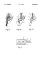
- FIG. 1a shows an inner layer of a conductor foil having printed circuit trace patternings.
- FIG. 1b shows a top view of the conductor foil.
- FIG. 1c shows a bottom view of the conductor foil.
- FIG. 2 shows a cross sectional view of a part of the conductor foil.
- FIGS. 1a, 1b and 1c show a cut-away portion of a conductor foil having a feed line segment 1.
- the conductor foil has, in a middle layer, thin copper printed circuit traces 7, 7', and 7", which, on the upper and lower sides, are covered by an elastically malleable polyimide layer 9, 10.
- the layered design of the conductor foil is schematically depicted in FIG. 2.
- Printed circuit traces 7 of feed line segment 1 are connected to soldering surfaces 8, which are provided for the soldering to the connecting pins of an undepicted electronic circuit carrier.
- Soldering surfaces 8 are designed in the shape of soldering eyelets.
- the printed circuit traces can be connected to soldering surfaces 8 on the upper side (FIG.
- FIGS. 1a, 1b and 1c show a stiffening segment 2 branching off from the feed line segment. Stiffening segment 2 has a large-surface printed circuit trace 7" on the inner layer of the conductor foil (FIG. 1a).
- a further printed circuit trace 7' which is connected to one of soldering surfaces 8 on feed line segment 1, via a narrow elastically malleable foil segment 14.
- a copper layer 12 which is covered by a tin layer 13.
- These metallic layers constitute a reinforcing layer, which increases the rigidity of the conductor foil in the area of stiffening segment 2.
- Metallic layers 12, 13 extend over entire stiffening segment 2 and over the part of feed line segment 1 which constitutes bonding area 5 of stiffening segment 2.
- an additional polyimide layer 11 is applied onto stiffening area 5, the polyimide layer at least partially covering the stiffening area.
- the polyimide layer also extends over bonding area 5 of feed line segment 1 and stiffening segment 2, and it has a greater thickness than polyimide layer 10.
- a connecting point 6 shaped as a circular opening. The inner wall of the opening is connected, via a through-plating, to printed circuit trace 7' and printed circuit trace 7".
- Stiffening segment 2 can be screwed, for example, to a housing part, using a screw passing through this opening.
- Edge 16 of tin-coated copper layer 12, 13 facing end 3 of feed line segment 1 is provided with a notched rim, to prevent a break of printed circuit traces 7 in the transitional area between the flexible conductor foil and the reinforced conductor foil.
- the conductor foil contacts a metallic housing wall in area a.
- Polyimide layer 11 and metallic layers 12, 13 advantageously generate an abrasion protection effect for the conductor foil.
Abstract
In a conductor foil for conductively connecting electrical and/or electronic components, the conductor foil including printed circuit traces, insulated to the outside and applied on a non-conductive, elastically malleable carrier foil. The conductive foil also includes soldering surfaces connected to the printed circuit traces, for soldering to electric terminals of components, in addition, the conductor foil includes feed line segments through which the printed circuit traces are led to the soldering surfaces, in order, in response to shaking stresses, to avoid damage to the soldering points by vibrations transmitted by the feed line segments. Furthermore, the conductor foil has stiffening segments branching off from the feed line segments, the stiffening segments, in response to shaking stresses, causing a force diversion of the vibrations onto the stiffening segments via the feed line segment movable end, which is not connected to the soldering surfaces.
Description
The present invention relates to a conductor foil for conductively connecting electrical and/or electronic components.
It is known to use conductor foils for electrically connecting electrical or electronic components. The conductor foils have a multilayer structure, printed circuit trace patternings, insulated to the outside, being applied to a nonconductive carrier foil. For example, it is known to apply thin copper printed circuit traces onto a carrier foil made of polyimide and to cover them with a further carrier foil. The printed circuit traces are conductively connected to the soldering surfaces arranged on the conductor foil for hard-soldering to the electrical terminals of components. Conductor foils of this type are employed, for example, near automobile engines or transmission units. Thus it is known, for example, to integrate a hybrid circuit in the housing of a clutch actuator, the hybrid circuit being connected, via a conductor foil, to various valves for regulating compressed air as well as to an eddy current sensor and to a plug-in part for connection to external cables. The hybrid circuit has a plug connector for this purpose, whose connector pins are soldered to the soldering surfaces of the conductor foil, which are designed as soldering eyelets. The elastically malleable conductor foils have great strength in the face of vibration stresses, but the most extreme shaking stresses arising in units of this type with acceleration up to 50 g, exert extremely heavy stresses on the soldering surfaces of the conductor foil. Vibration stresses, which are transmitted to the plug connector via a vibrating feed line segment of the conductor foil, can lead to the soldering points breaking or individual connecting pins being broken from the plug connector.
The conductor foil of the present invention has an advantage that the forces exerted by the vibrations of a feed line segment of the conductor foil are not transmitted to the soldering surfaces of the conductor foil, and, in this way, damage to the soldering points is avoided and the reliability of the electrical connection is increased. This is achieved by providing for at least one stiffening segment branching off from the feed line segment, the stiffening segment bringing about a diversion of the forces of vibrations transmitted to the stiffening segment, via the movable end of the feed line segment, which is not connected to the soldering surfaces.
It is particularly advantageous, as a means of force diversion, to arrange on the conductor foil at least one reinforcing layer to stiffen the elastically malleable conductor foil, the stiffening layer covering the feed line segment in the bonding area of the feed line segment and extending at least partly over the stiffening segment. The reinforcing layer can be applied to the conductor foil using conventional production methods in a simple manner.
Furthermore, it is advantageous to integrate a connecting point into the stiffening segment, the connecting point being spatially separate from the soldering points of the feed line segment and able to be connected to a connecting means. The connecting point can be affixed to a housing part, for example, using a screw or a corresponding aid. Then, in response to vibration stresses, the forces of the conductor foil feed line segment, acting upon the stiffening segment, are transmitted to the screw connected to the connecting point.
The reinforcing layer can advantageously be an additional polyimide layer and/or a metallic layer applied on the conductor foil, e.g., a tin-coated copper layer. These layers can advantageously produce an abrasion protection effect for the conductor foil at such points where the conductor foil contacts housing parts. During the production of the conductor foil, the tin-coated copper layer, together with the soldering surfaces provided for the connection to the components, can be produced in a simple manner.
It is particularly advantageous to provide the connecting point as a ground for the components connected to the soldering points. For this purpose, provision is made for a further elastically malleable foil segment containing a single grounding printed circuit trace and connecting a soldering surface, soldered to a grounding pin of the component, to the connecting point. In the case of relative movement, arising in response to vibration, between the connecting point, affixed to a housing part, and the soldering points of the components, no force is transmitted by the elastic foil segment to the sensitive soldering points.
It is also advantageous to design the edge of the reinforcing layer, facing the movable part of the feed line segment, with a notched contour, to obtain a smooth transition from the reinforcing area to the elastically malleable area of the feed line segment, and to avoid a break in the printed circuit trace at this location.
FIG. 1a shows an inner layer of a conductor foil having printed circuit trace patternings.
FIG. 1b shows a top view of the conductor foil.
FIG. 1c shows a bottom view of the conductor foil.
FIG. 2 shows a cross sectional view of a part of the conductor foil.
FIGS. 1a, 1b and 1c show a cut-away portion of a conductor foil having a feed line segment 1. As illustrated in FIG. 1a, the conductor foil has, in a middle layer, thin copper printed circuit traces 7, 7', and 7", which, on the upper and lower sides, are covered by an elastically malleable polyimide layer 9, 10. The layered design of the conductor foil is schematically depicted in FIG. 2. Printed circuit traces 7 of feed line segment 1 are connected to soldering surfaces 8, which are provided for the soldering to the connecting pins of an undepicted electronic circuit carrier. Soldering surfaces 8 are designed in the shape of soldering eyelets. The printed circuit traces can be connected to soldering surfaces 8 on the upper side (FIG. 1b), for example, via metal-coated through holes, in a conventional manner. When the conductor foil is connected to a circuit carrier, e.g., a hybrid circuit, the connecting pins of the hybrid circuit are led through the through holes and are soldered to the soldering eyelets. In response to shaking stress on the arrangement, end 3 of feed line segment 1, which is freely movable, elastically malleable, and connected to the other feed line segments of the conductor foil, oscillates or vibrates. FIGS. 1a, 1b and 1c show a stiffening segment 2 branching off from the feed line segment. Stiffening segment 2 has a large-surface printed circuit trace 7" on the inner layer of the conductor foil (FIG. 1a). To large-surface printed circuit trace 7" is connected a further printed circuit trace 7', which is connected to one of soldering surfaces 8 on feed line segment 1, via a narrow elastically malleable foil segment 14. As illustrated in FIG. 1b and FIG. 2, provision is made on the upper side of the conductor foil for a copper layer 12, which is covered by a tin layer 13. These metallic layers constitute a reinforcing layer, which increases the rigidity of the conductor foil in the area of stiffening segment 2. Metallic layers 12, 13 extend over entire stiffening segment 2 and over the part of feed line segment 1 which constitutes bonding area 5 of stiffening segment 2. On the reverse side of the conductor foil, as illustrated in FIG. 1c and FIG. 2, an additional polyimide layer 11 is applied onto stiffening area 5, the polyimide layer at least partially covering the stiffening area. The polyimide layer also extends over bonding area 5 of feed line segment 1 and stiffening segment 2, and it has a greater thickness than polyimide layer 10. Arranged in stiffening segment 2 is a connecting point 6 shaped as a circular opening. The inner wall of the opening is connected, via a through-plating, to printed circuit trace 7' and printed circuit trace 7". Stiffening segment 2 can be screwed, for example, to a housing part, using a screw passing through this opening. Via printed circuit trace 7', a ground is then simultaneously achieved, both of soldering surface 8, connected to this printed circuit trace, and of the connecting pin of the hybrid circuit, connected thereto. When the arrangement undergoes vibration or shaking stresses, the force of acceleration is now exerted via freely movable end 3 of feed line segment 1 onto reinforcing layers 11, 12, and 13, and is diverted from them to connecting point 6, so that soldering surfaces 8 are relieved of strain and no great stresses are transmitted to them. At the same time, elastic foil segment 14 having the grounding printed circuit trace permits relative movement between connecting point 6 of the stiffening segment and soldering surfaces 8, without diverting force onto the plug connector of the hybrid. Edge 16 of tin-coated copper layer 12, 13 facing end 3 of feed line segment 1 is provided with a notched rim, to prevent a break of printed circuit traces 7 in the transitional area between the flexible conductor foil and the reinforced conductor foil. In the exemplary embodiment shown here, the conductor foil contacts a metallic housing wall in area a. Polyimide layer 11 and metallic layers 12, 13 advantageously generate an abrasion protection effect for the conductor foil.
Claims (9)
1. A conductor foil for conductively connecting electrical components, comprising:
printed circuit traces insulated on an outer side of the conductor foil and applied on a non-conductive carrier foil, the non-conductive carrier foil being elastically malleable;
at least one feed line segment;
soldering surfaces coupled to the printed circuit traces via the at least one feed line segment for soldering to the electrical components; and
at least one stiffening segment extending away from the at least one feed line segment, the at least one stiffening segment adapted for being coupled to a connecting point outside of the electrical components soldered to the soldering surfaces;
wherein shaking stresses generated by vibrations on a movable end of the at least one feed line segment, which is not connected to the soldering surfaces, are diverted away from the soldering surfaces and transmitted to the at least one stiffening segment and to said connecting point.
2. The conductor foil according to claim 1, further comprising:
at least one reinforcing layer partly extending over the at least one stiffening segment and the at least one feed line segment in a common bonding area.
3. The conductor foil according to claim 2, wherein an edge of the at least one reinforcing layer is positioned toward the moveable end.
4. The conductor foil according to claim 2, wherein the at least one reinforcing layer includes at least one of a metallic layer and a non-conductive plastic layer applied onto the conductor foil.
5. The conductor foil according to claim 4, wherein the metallic layer is composed of a copper layer coated with a tin material.
6. The conductor foil according to claim 4, wherein the non-conductive plastic layer is composed of a polyimide material.
7. The conductor foil according to claim 1, wherein the connecting point provides a ground connection for the electrical components.
8. The conductor foil according to claim 1, wherein at least one of the soldering surfaces is coupled to the connecting point via a foil segment, the foil segment including one of the printed circuit traces coupled to the at least one feed line segment.
9. The conductor foil according to claim 8, wherein at least one of the soldering surfaces is coupled to a ground connection of the electrical components, and wherein the printed circuit traces include a grounding printed circuit trace coupled to one of the soldering surfaces.
Applications Claiming Priority (3)
| Application Number | Priority Date | Filing Date | Title |
|---|---|---|---|
| DE19653360A DE19653360A1 (en) | 1996-12-20 | 1996-12-20 | Conductive foil for the conductive connection of electrical and / or electronic components |
| DE19653360 | 1996-12-20 | ||
| PCT/DE1997/001995 WO1998028956A1 (en) | 1996-12-20 | 1997-09-09 | Conducting foil for conductively connecting electric and/or electronic components |
Publications (1)
| Publication Number | Publication Date |
|---|---|
| US6150614A true US6150614A (en) | 2000-11-21 |
Family
ID=7815582
Family Applications (1)
| Application Number | Title | Priority Date | Filing Date |
|---|---|---|---|
| US09/125,183 Expired - Lifetime US6150614A (en) | 1996-12-20 | 1997-09-09 | Conducting foil for conductively connecting electric and/or electronic components |
Country Status (5)
| Country | Link |
|---|---|
| US (1) | US6150614A (en) |
| EP (1) | EP0886991B1 (en) |
| JP (1) | JP3850449B2 (en) |
| DE (2) | DE19653360A1 (en) |
| WO (1) | WO1998028956A1 (en) |
Cited By (7)
| Publication number | Priority date | Publication date | Assignee | Title |
|---|---|---|---|---|
| US6348661B1 (en) * | 2000-08-11 | 2002-02-19 | Magnecomp Corp. | Corrosion protection for wireless flexure |
| US6740824B2 (en) * | 2002-06-25 | 2004-05-25 | Motorola, Inc. | Ground connector assembly with substrate strain relief and method of making same |
| US20060176625A1 (en) * | 2005-02-04 | 2006-08-10 | Shander Mark S | Circuit protection devices having an integral barrier with grounding provision |
| US7407408B1 (en) | 2006-12-22 | 2008-08-05 | Amphenol Corporation | Flexible circuit connector assembly with strain relief |
| US20110216445A1 (en) * | 2010-03-02 | 2011-09-08 | Kabushiki Kaisha Toshiba | Electronic substrate and magnetic disk apparatus |
| EP3598855A4 (en) * | 2017-08-23 | 2020-05-13 | Kunshan Go-Visionox Opto-Electronics Co., Ltd. | Positioning structure and flexible circuit board |
| US10673165B1 (en) * | 2019-07-05 | 2020-06-02 | Wbstudio Technology Media Co., Ltd. | Power connector for building blocks |
Families Citing this family (1)
| Publication number | Priority date | Publication date | Assignee | Title |
|---|---|---|---|---|
| DE10011373A1 (en) * | 2000-03-09 | 2001-09-13 | Delphi Tech Inc | Flexible printed circuit used in the production of an instrument panel for vehicles consists of a base material, a conductor pattern applied on one side, and a flexible or semi-flexible reinforcing material applied on the other side |
Citations (14)
| Publication number | Priority date | Publication date | Assignee | Title |
|---|---|---|---|---|
| US4127740A (en) * | 1977-08-17 | 1978-11-28 | Sheldahl, Inc. | Routing arrangement for ground conductors in printed circuit structures |
| USH416H (en) * | 1981-08-31 | 1988-01-05 | Rogers Corporation | High capacitance flexible circuit |
| US4937707A (en) * | 1988-05-26 | 1990-06-26 | International Business Machines Corporation | Flexible carrier for an electronic device |
| JPH03104755A (en) * | 1989-09-16 | 1991-05-01 | Aisin Seiki Co Ltd | Current feed device for ultrasonic vibrator |
| US5296831A (en) * | 1989-10-02 | 1994-03-22 | Deutsch Thomson Brandt Gmbh | Coil arrangement for a focusing or track control circuit |
| US5384690A (en) * | 1993-07-27 | 1995-01-24 | International Business Machines Corporation | Flex laminate package for a parallel processor |
| EP0635995A1 (en) * | 1993-07-22 | 1995-01-25 | Societe D'applications Generales D'electricite Et De Mecanique Sagem | Flexible circuit for connecting printed circuit |
| US5495076A (en) * | 1993-10-18 | 1996-02-27 | Ford Motor Company | Flexible geometry circuit board |
| US5585157A (en) * | 1994-02-14 | 1996-12-17 | Nikon Corporation | Printed susbstrate having reinforcement patterns of varying size and/or shape |
| US5723205A (en) * | 1994-03-08 | 1998-03-03 | Teledyne Industries, Inc. | Fabrication multilayer combined rigid/flex printer circuit board |
| US5737053A (en) * | 1995-06-05 | 1998-04-07 | Kabushiki Kaisha Toshiba | Wire substrate having branch lines perpendicular to the main lines in which the branch lines connect to driving circuits on a display device |
| US5742480A (en) * | 1994-11-02 | 1998-04-21 | Sumitomo Electric Industries, Ltd. | Optical module circuit board having flexible structure |
| US5764497A (en) * | 1995-11-13 | 1998-06-09 | Minolta Co, Ltd. | Circuit board connection method and connection structure |
| US5777855A (en) * | 1996-06-18 | 1998-07-07 | Eastman Kodak Company | Method and apparatus for connecting flexible circuits to printed circuit boards |
Family Cites Families (1)
| Publication number | Priority date | Publication date | Assignee | Title |
|---|---|---|---|---|
| JPH0946004A (en) * | 1995-08-01 | 1997-02-14 | Sumitomo Wiring Syst Ltd | Flexible printed board |
-
1996
- 1996-12-20 DE DE19653360A patent/DE19653360A1/en not_active Ceased
-
1997
- 1997-09-09 US US09/125,183 patent/US6150614A/en not_active Expired - Lifetime
- 1997-09-09 JP JP52819398A patent/JP3850449B2/en not_active Expired - Fee Related
- 1997-09-09 EP EP97943746A patent/EP0886991B1/en not_active Expired - Lifetime
- 1997-09-09 DE DE59712043T patent/DE59712043D1/en not_active Expired - Lifetime
- 1997-09-09 WO PCT/DE1997/001995 patent/WO1998028956A1/en active IP Right Grant
Patent Citations (14)
| Publication number | Priority date | Publication date | Assignee | Title |
|---|---|---|---|---|
| US4127740A (en) * | 1977-08-17 | 1978-11-28 | Sheldahl, Inc. | Routing arrangement for ground conductors in printed circuit structures |
| USH416H (en) * | 1981-08-31 | 1988-01-05 | Rogers Corporation | High capacitance flexible circuit |
| US4937707A (en) * | 1988-05-26 | 1990-06-26 | International Business Machines Corporation | Flexible carrier for an electronic device |
| JPH03104755A (en) * | 1989-09-16 | 1991-05-01 | Aisin Seiki Co Ltd | Current feed device for ultrasonic vibrator |
| US5296831A (en) * | 1989-10-02 | 1994-03-22 | Deutsch Thomson Brandt Gmbh | Coil arrangement for a focusing or track control circuit |
| EP0635995A1 (en) * | 1993-07-22 | 1995-01-25 | Societe D'applications Generales D'electricite Et De Mecanique Sagem | Flexible circuit for connecting printed circuit |
| US5384690A (en) * | 1993-07-27 | 1995-01-24 | International Business Machines Corporation | Flex laminate package for a parallel processor |
| US5495076A (en) * | 1993-10-18 | 1996-02-27 | Ford Motor Company | Flexible geometry circuit board |
| US5585157A (en) * | 1994-02-14 | 1996-12-17 | Nikon Corporation | Printed susbstrate having reinforcement patterns of varying size and/or shape |
| US5723205A (en) * | 1994-03-08 | 1998-03-03 | Teledyne Industries, Inc. | Fabrication multilayer combined rigid/flex printer circuit board |
| US5742480A (en) * | 1994-11-02 | 1998-04-21 | Sumitomo Electric Industries, Ltd. | Optical module circuit board having flexible structure |
| US5737053A (en) * | 1995-06-05 | 1998-04-07 | Kabushiki Kaisha Toshiba | Wire substrate having branch lines perpendicular to the main lines in which the branch lines connect to driving circuits on a display device |
| US5764497A (en) * | 1995-11-13 | 1998-06-09 | Minolta Co, Ltd. | Circuit board connection method and connection structure |
| US5777855A (en) * | 1996-06-18 | 1998-07-07 | Eastman Kodak Company | Method and apparatus for connecting flexible circuits to printed circuit boards |
Non-Patent Citations (4)
| Title |
|---|
| Copy of reference not enclosed originally forwarded with Search Report by International Searching Authority C.D. Keirstead, Flexible Printed Circuits: A Design Primer , Assembly Engineering, Bd. 31, No. 5, 1988, pp. 32 36. * |
| Copy of reference not enclosed originally forwarded with Search Report by International Searching Authority Patent Abstracts of Japan, vol. 15, No. 290 (M 1139), Jul. 23, 1991 & JP 03 104755, May 1, 1991. * |
| Copy of reference not enclosed--originally forwarded with Search Report by International Searching Authority C.D. Keirstead, "Flexible Printed Circuits: A Design Primer", Assembly Engineering, Bd. 31, No. 5, 1988, pp. 32-36. |
| Copy of reference not enclosed--originally forwarded with Search Report by International Searching Authority Patent Abstracts of Japan, vol. 15, No. 290 (M-1139), Jul. 23, 1991 & JP 03 104755, May 1, 1991. |
Cited By (9)
| Publication number | Priority date | Publication date | Assignee | Title |
|---|---|---|---|---|
| US6348661B1 (en) * | 2000-08-11 | 2002-02-19 | Magnecomp Corp. | Corrosion protection for wireless flexure |
| US6740824B2 (en) * | 2002-06-25 | 2004-05-25 | Motorola, Inc. | Ground connector assembly with substrate strain relief and method of making same |
| EP1376778A3 (en) * | 2002-06-25 | 2007-01-03 | Motorola, Inc. | Ground connector assembly with substrate strain relief and method of making the same |
| US20060176625A1 (en) * | 2005-02-04 | 2006-08-10 | Shander Mark S | Circuit protection devices having an integral barrier with grounding provision |
| US7407408B1 (en) | 2006-12-22 | 2008-08-05 | Amphenol Corporation | Flexible circuit connector assembly with strain relief |
| US20110216445A1 (en) * | 2010-03-02 | 2011-09-08 | Kabushiki Kaisha Toshiba | Electronic substrate and magnetic disk apparatus |
| US8300365B2 (en) * | 2010-03-02 | 2012-10-30 | Kabushiki Kaisha Toshiba | Electronic substrate and magnetic disk apparatus |
| EP3598855A4 (en) * | 2017-08-23 | 2020-05-13 | Kunshan Go-Visionox Opto-Electronics Co., Ltd. | Positioning structure and flexible circuit board |
| US10673165B1 (en) * | 2019-07-05 | 2020-06-02 | Wbstudio Technology Media Co., Ltd. | Power connector for building blocks |
Also Published As
| Publication number | Publication date |
|---|---|
| JP2000505952A (en) | 2000-05-16 |
| EP0886991B1 (en) | 2004-10-27 |
| WO1998028956A1 (en) | 1998-07-02 |
| EP0886991A1 (en) | 1998-12-30 |
| DE59712043D1 (en) | 2004-12-02 |
| DE19653360A1 (en) | 1998-06-25 |
| JP3850449B2 (en) | 2006-11-29 |
Similar Documents
| Publication | Publication Date | Title |
|---|---|---|
| US6028770A (en) | Control device, especially for a motor vehicle | |
| US6233153B1 (en) | Subassembly having a housing with an integral electrical plug unit | |
| US5414220A (en) | Flexible wiring cable | |
| US20040200279A1 (en) | Composite sensor for detecting angular velocity and acceleration | |
| US7393240B2 (en) | Electrical connector | |
| US5408052A (en) | Flexible multi-layer circuit wiring board | |
| US5053923A (en) | Electronic control unit with common ground connection to a heat sink | |
| US5151771A (en) | High lead count circuit board for connecting electronic components to an external circuit | |
| CN1050452C (en) | Device for controlling motor vehicle | |
| US6150614A (en) | Conducting foil for conductively connecting electric and/or electronic components | |
| EP0952545A4 (en) | Ic card | |
| US4885662A (en) | Circuit module connection system | |
| CA2310765A1 (en) | Stress relaxation type electronic component, a stress relaxation type circuit board, and a stress relaxation type electronic component mounted member | |
| EP0330372A3 (en) | Hybrid ic with heat sink | |
| EP1020908A4 (en) | Resin-sealed surface mounting type electronic parts | |
| EP1403967A3 (en) | Connecting structure for accessory device and cable waterproofing structure for accessory device and mounting structure for accessory device | |
| JP2003257397A (en) | Terminal for button type battery | |
| US20030160313A1 (en) | Semiconductor device | |
| JP7049897B2 (en) | Antenna module | |
| US10644423B2 (en) | Semiconductor module | |
| EP0854667B1 (en) | Electronic control module | |
| US10693247B2 (en) | Fixation structure | |
| EP1471605A3 (en) | Electronic circuit unit having mounting structure with high soldering reliability | |
| US20030150634A1 (en) | Undetachable electrical and mechnical connection, contact element for an undetachable electrical and mechanical connection, and method of producing such an electrical and mechanical connection | |
| JP2000503470A (en) | Electric circuit and control device |
Legal Events
| Date | Code | Title | Description |
|---|---|---|---|
| AS | Assignment |
Owner name: ROBERT BOSCH GMBH, GERMANY Free format text: ASSIGNMENT OF ASSIGNORS INTEREST;ASSIGNORS:MILLER, BERNHARD;ROETHER, FRIEDBERT;SCHNEIDER, NORBERT;REEL/FRAME:009852/0403;SIGNING DATES FROM 19980702 TO 19980703 |
|
| STCF | Information on status: patent grant |
Free format text: PATENTED CASE |
|
| FEPP | Fee payment procedure |
Free format text: PAYOR NUMBER ASSIGNED (ORIGINAL EVENT CODE: ASPN); ENTITY STATUS OF PATENT OWNER: LARGE ENTITY |
|
| FPAY | Fee payment |
Year of fee payment: 4 |
|
| FPAY | Fee payment |
Year of fee payment: 8 |
|
| FPAY | Fee payment |
Year of fee payment: 12 |