US6150716A - Metal substrate having an IC chip and carrier mounting - Google Patents
Metal substrate having an IC chip and carrier mounting Download PDFInfo
- Publication number
- US6150716A US6150716A US08/783,775 US78377597A US6150716A US 6150716 A US6150716 A US 6150716A US 78377597 A US78377597 A US 78377597A US 6150716 A US6150716 A US 6150716A
- Authority
- US
- United States
- Prior art keywords
- chip
- substrate
- package according
- thickness
- pads
- Prior art date
- Legal status (The legal status is an assumption and is not a legal conclusion. Google has not performed a legal analysis and makes no representation as to the accuracy of the status listed.)
- Expired - Fee Related
Links
Images
Classifications
-
- H—ELECTRICITY
- H01—ELECTRIC ELEMENTS
- H01L—SEMICONDUCTOR DEVICES NOT COVERED BY CLASS H10
- H01L23/00—Details of semiconductor or other solid state devices
- H01L23/28—Encapsulations, e.g. encapsulating layers, coatings, e.g. for protection
- H01L23/29—Encapsulations, e.g. encapsulating layers, coatings, e.g. for protection characterised by the material, e.g. carbon
- H01L23/293—Organic, e.g. plastic
-
- H—ELECTRICITY
- H01—ELECTRIC ELEMENTS
- H01L—SEMICONDUCTOR DEVICES NOT COVERED BY CLASS H10
- H01L21/00—Processes or apparatus adapted for the manufacture or treatment of semiconductor or solid state devices or of parts thereof
- H01L21/02—Manufacture or treatment of semiconductor devices or of parts thereof
- H01L21/04—Manufacture or treatment of semiconductor devices or of parts thereof the devices having at least one potential-jump barrier or surface barrier, e.g. PN junction, depletion layer or carrier concentration layer
- H01L21/50—Assembly of semiconductor devices using processes or apparatus not provided for in a single one of the subgroups H01L21/06 - H01L21/326, e.g. sealing of a cap to a base of a container
- H01L21/56—Encapsulations, e.g. encapsulation layers, coatings
- H01L21/563—Encapsulation of active face of flip-chip device, e.g. underfilling or underencapsulation of flip-chip, encapsulation preform on chip or mounting substrate
-
- H—ELECTRICITY
- H01—ELECTRIC ELEMENTS
- H01L—SEMICONDUCTOR DEVICES NOT COVERED BY CLASS H10
- H01L23/00—Details of semiconductor or other solid state devices
- H01L23/12—Mountings, e.g. non-detachable insulating substrates
- H01L23/14—Mountings, e.g. non-detachable insulating substrates characterised by the material or its electrical properties
- H01L23/142—Metallic substrates having insulating layers
-
- H—ELECTRICITY
- H01—ELECTRIC ELEMENTS
- H01L—SEMICONDUCTOR DEVICES NOT COVERED BY CLASS H10
- H01L23/00—Details of semiconductor or other solid state devices
- H01L23/28—Encapsulations, e.g. encapsulating layers, coatings, e.g. for protection
- H01L23/31—Encapsulations, e.g. encapsulating layers, coatings, e.g. for protection characterised by the arrangement or shape
- H01L23/3107—Encapsulations, e.g. encapsulating layers, coatings, e.g. for protection characterised by the arrangement or shape the device being completely enclosed
- H01L23/3121—Encapsulations, e.g. encapsulating layers, coatings, e.g. for protection characterised by the arrangement or shape the device being completely enclosed a substrate forming part of the encapsulation
-
- H—ELECTRICITY
- H01—ELECTRIC ELEMENTS
- H01L—SEMICONDUCTOR DEVICES NOT COVERED BY CLASS H10
- H01L23/00—Details of semiconductor or other solid state devices
- H01L23/48—Arrangements for conducting electric current to or from the solid state body in operation, e.g. leads, terminal arrangements ; Selection of materials therefor
- H01L23/488—Arrangements for conducting electric current to or from the solid state body in operation, e.g. leads, terminal arrangements ; Selection of materials therefor consisting of soldered or bonded constructions
- H01L23/498—Leads, i.e. metallisations or lead-frames on insulating substrates, e.g. chip carriers
- H01L23/49811—Additional leads joined to the metallisation on the insulating substrate, e.g. pins, bumps, wires, flat leads
- H01L23/49816—Spherical bumps on the substrate for external connection, e.g. ball grid arrays [BGA]
-
- H—ELECTRICITY
- H01—ELECTRIC ELEMENTS
- H01L—SEMICONDUCTOR DEVICES NOT COVERED BY CLASS H10
- H01L23/00—Details of semiconductor or other solid state devices
- H01L23/48—Arrangements for conducting electric current to or from the solid state body in operation, e.g. leads, terminal arrangements ; Selection of materials therefor
- H01L23/488—Arrangements for conducting electric current to or from the solid state body in operation, e.g. leads, terminal arrangements ; Selection of materials therefor consisting of soldered or bonded constructions
- H01L23/498—Leads, i.e. metallisations or lead-frames on insulating substrates, e.g. chip carriers
- H01L23/49822—Multilayer substrates
-
- H—ELECTRICITY
- H01—ELECTRIC ELEMENTS
- H01L—SEMICONDUCTOR DEVICES NOT COVERED BY CLASS H10
- H01L23/00—Details of semiconductor or other solid state devices
- H01L23/52—Arrangements for conducting electric current within the device in operation from one component to another, i.e. interconnections, e.g. wires, lead frames
- H01L23/538—Arrangements for conducting electric current within the device in operation from one component to another, i.e. interconnections, e.g. wires, lead frames the interconnection structure between a plurality of semiconductor chips being formed on, or in, insulating substrates
- H01L23/5385—Assembly of a plurality of insulating substrates
-
- H—ELECTRICITY
- H01—ELECTRIC ELEMENTS
- H01L—SEMICONDUCTOR DEVICES NOT COVERED BY CLASS H10
- H01L24/00—Arrangements for connecting or disconnecting semiconductor or solid-state bodies; Methods or apparatus related thereto
- H01L24/01—Means for bonding being attached to, or being formed on, the surface to be connected, e.g. chip-to-package, die-attach, "first-level" interconnects; Manufacturing methods related thereto
- H01L24/26—Layer connectors, e.g. plate connectors, solder or adhesive layers; Manufacturing methods related thereto
- H01L24/31—Structure, shape, material or disposition of the layer connectors after the connecting process
- H01L24/32—Structure, shape, material or disposition of the layer connectors after the connecting process of an individual layer connector
-
- H—ELECTRICITY
- H01—ELECTRIC ELEMENTS
- H01L—SEMICONDUCTOR DEVICES NOT COVERED BY CLASS H10
- H01L2224/00—Indexing scheme for arrangements for connecting or disconnecting semiconductor or solid-state bodies and methods related thereto as covered by H01L24/00
- H01L2224/01—Means for bonding being attached to, or being formed on, the surface to be connected, e.g. chip-to-package, die-attach, "first-level" interconnects; Manufacturing methods related thereto
- H01L2224/02—Bonding areas; Manufacturing methods related thereto
- H01L2224/04—Structure, shape, material or disposition of the bonding areas prior to the connecting process
- H01L2224/05—Structure, shape, material or disposition of the bonding areas prior to the connecting process of an individual bonding area
- H01L2224/0554—External layer
- H01L2224/05599—Material
-
- H—ELECTRICITY
- H01—ELECTRIC ELEMENTS
- H01L—SEMICONDUCTOR DEVICES NOT COVERED BY CLASS H10
- H01L2224/00—Indexing scheme for arrangements for connecting or disconnecting semiconductor or solid-state bodies and methods related thereto as covered by H01L24/00
- H01L2224/01—Means for bonding being attached to, or being formed on, the surface to be connected, e.g. chip-to-package, die-attach, "first-level" interconnects; Manufacturing methods related thereto
- H01L2224/10—Bump connectors; Manufacturing methods related thereto
- H01L2224/15—Structure, shape, material or disposition of the bump connectors after the connecting process
- H01L2224/16—Structure, shape, material or disposition of the bump connectors after the connecting process of an individual bump connector
- H01L2224/161—Disposition
- H01L2224/16151—Disposition the bump connector connecting between a semiconductor or solid-state body and an item not being a semiconductor or solid-state body, e.g. chip-to-substrate, chip-to-passive
- H01L2224/16221—Disposition the bump connector connecting between a semiconductor or solid-state body and an item not being a semiconductor or solid-state body, e.g. chip-to-substrate, chip-to-passive the body and the item being stacked
- H01L2224/16225—Disposition the bump connector connecting between a semiconductor or solid-state body and an item not being a semiconductor or solid-state body, e.g. chip-to-substrate, chip-to-passive the body and the item being stacked the item being non-metallic, e.g. insulating substrate with or without metallisation
-
- H—ELECTRICITY
- H01—ELECTRIC ELEMENTS
- H01L—SEMICONDUCTOR DEVICES NOT COVERED BY CLASS H10
- H01L2224/00—Indexing scheme for arrangements for connecting or disconnecting semiconductor or solid-state bodies and methods related thereto as covered by H01L24/00
- H01L2224/01—Means for bonding being attached to, or being formed on, the surface to be connected, e.g. chip-to-package, die-attach, "first-level" interconnects; Manufacturing methods related thereto
- H01L2224/26—Layer connectors, e.g. plate connectors, solder or adhesive layers; Manufacturing methods related thereto
- H01L2224/27—Manufacturing methods
- H01L2224/27011—Involving a permanent auxiliary member, i.e. a member which is left at least partly in the finished device, e.g. coating, dummy feature
- H01L2224/27013—Involving a permanent auxiliary member, i.e. a member which is left at least partly in the finished device, e.g. coating, dummy feature for holding or confining the layer connector, e.g. solder flow barrier
-
- H—ELECTRICITY
- H01—ELECTRIC ELEMENTS
- H01L—SEMICONDUCTOR DEVICES NOT COVERED BY CLASS H10
- H01L2224/00—Indexing scheme for arrangements for connecting or disconnecting semiconductor or solid-state bodies and methods related thereto as covered by H01L24/00
- H01L2224/01—Means for bonding being attached to, or being formed on, the surface to be connected, e.g. chip-to-package, die-attach, "first-level" interconnects; Manufacturing methods related thereto
- H01L2224/26—Layer connectors, e.g. plate connectors, solder or adhesive layers; Manufacturing methods related thereto
- H01L2224/31—Structure, shape, material or disposition of the layer connectors after the connecting process
- H01L2224/32—Structure, shape, material or disposition of the layer connectors after the connecting process of an individual layer connector
- H01L2224/321—Disposition
- H01L2224/32151—Disposition the layer connector connecting between a semiconductor or solid-state body and an item not being a semiconductor or solid-state body, e.g. chip-to-substrate, chip-to-passive
- H01L2224/32221—Disposition the layer connector connecting between a semiconductor or solid-state body and an item not being a semiconductor or solid-state body, e.g. chip-to-substrate, chip-to-passive the body and the item being stacked
- H01L2224/32225—Disposition the layer connector connecting between a semiconductor or solid-state body and an item not being a semiconductor or solid-state body, e.g. chip-to-substrate, chip-to-passive the body and the item being stacked the item being non-metallic, e.g. insulating substrate with or without metallisation
-
- H—ELECTRICITY
- H01—ELECTRIC ELEMENTS
- H01L—SEMICONDUCTOR DEVICES NOT COVERED BY CLASS H10
- H01L2224/00—Indexing scheme for arrangements for connecting or disconnecting semiconductor or solid-state bodies and methods related thereto as covered by H01L24/00
- H01L2224/01—Means for bonding being attached to, or being formed on, the surface to be connected, e.g. chip-to-package, die-attach, "first-level" interconnects; Manufacturing methods related thereto
- H01L2224/42—Wire connectors; Manufacturing methods related thereto
- H01L2224/47—Structure, shape, material or disposition of the wire connectors after the connecting process
- H01L2224/48—Structure, shape, material or disposition of the wire connectors after the connecting process of an individual wire connector
- H01L2224/4805—Shape
- H01L2224/4809—Loop shape
- H01L2224/48091—Arched
-
- H—ELECTRICITY
- H01—ELECTRIC ELEMENTS
- H01L—SEMICONDUCTOR DEVICES NOT COVERED BY CLASS H10
- H01L2224/00—Indexing scheme for arrangements for connecting or disconnecting semiconductor or solid-state bodies and methods related thereto as covered by H01L24/00
- H01L2224/01—Means for bonding being attached to, or being formed on, the surface to be connected, e.g. chip-to-package, die-attach, "first-level" interconnects; Manufacturing methods related thereto
- H01L2224/42—Wire connectors; Manufacturing methods related thereto
- H01L2224/47—Structure, shape, material or disposition of the wire connectors after the connecting process
- H01L2224/48—Structure, shape, material or disposition of the wire connectors after the connecting process of an individual wire connector
- H01L2224/481—Disposition
- H01L2224/48151—Connecting between a semiconductor or solid-state body and an item not being a semiconductor or solid-state body, e.g. chip-to-substrate, chip-to-passive
- H01L2224/48221—Connecting between a semiconductor or solid-state body and an item not being a semiconductor or solid-state body, e.g. chip-to-substrate, chip-to-passive the body and the item being stacked
- H01L2224/48225—Connecting between a semiconductor or solid-state body and an item not being a semiconductor or solid-state body, e.g. chip-to-substrate, chip-to-passive the body and the item being stacked the item being non-metallic, e.g. insulating substrate with or without metallisation
- H01L2224/48227—Connecting between a semiconductor or solid-state body and an item not being a semiconductor or solid-state body, e.g. chip-to-substrate, chip-to-passive the body and the item being stacked the item being non-metallic, e.g. insulating substrate with or without metallisation connecting the wire to a bond pad of the item
-
- H—ELECTRICITY
- H01—ELECTRIC ELEMENTS
- H01L—SEMICONDUCTOR DEVICES NOT COVERED BY CLASS H10
- H01L2224/00—Indexing scheme for arrangements for connecting or disconnecting semiconductor or solid-state bodies and methods related thereto as covered by H01L24/00
- H01L2224/01—Means for bonding being attached to, or being formed on, the surface to be connected, e.g. chip-to-package, die-attach, "first-level" interconnects; Manufacturing methods related thereto
- H01L2224/42—Wire connectors; Manufacturing methods related thereto
- H01L2224/47—Structure, shape, material or disposition of the wire connectors after the connecting process
- H01L2224/48—Structure, shape, material or disposition of the wire connectors after the connecting process of an individual wire connector
- H01L2224/484—Connecting portions
- H01L2224/48463—Connecting portions the connecting portion on the bonding area of the semiconductor or solid-state body being a ball bond
- H01L2224/48465—Connecting portions the connecting portion on the bonding area of the semiconductor or solid-state body being a ball bond the other connecting portion not on the bonding area being a wedge bond, i.e. ball-to-wedge, regular stitch
-
- H—ELECTRICITY
- H01—ELECTRIC ELEMENTS
- H01L—SEMICONDUCTOR DEVICES NOT COVERED BY CLASS H10
- H01L2224/00—Indexing scheme for arrangements for connecting or disconnecting semiconductor or solid-state bodies and methods related thereto as covered by H01L24/00
- H01L2224/01—Means for bonding being attached to, or being formed on, the surface to be connected, e.g. chip-to-package, die-attach, "first-level" interconnects; Manufacturing methods related thereto
- H01L2224/42—Wire connectors; Manufacturing methods related thereto
- H01L2224/47—Structure, shape, material or disposition of the wire connectors after the connecting process
- H01L2224/49—Structure, shape, material or disposition of the wire connectors after the connecting process of a plurality of wire connectors
- H01L2224/491—Disposition
- H01L2224/4912—Layout
- H01L2224/49175—Parallel arrangements
-
- H—ELECTRICITY
- H01—ELECTRIC ELEMENTS
- H01L—SEMICONDUCTOR DEVICES NOT COVERED BY CLASS H10
- H01L2224/00—Indexing scheme for arrangements for connecting or disconnecting semiconductor or solid-state bodies and methods related thereto as covered by H01L24/00
- H01L2224/73—Means for bonding being of different types provided for in two or more of groups H01L2224/10, H01L2224/18, H01L2224/26, H01L2224/34, H01L2224/42, H01L2224/50, H01L2224/63, H01L2224/71
- H01L2224/732—Location after the connecting process
- H01L2224/73201—Location after the connecting process on the same surface
- H01L2224/73203—Bump and layer connectors
- H01L2224/73204—Bump and layer connectors the bump connector being embedded into the layer connector
-
- H—ELECTRICITY
- H01—ELECTRIC ELEMENTS
- H01L—SEMICONDUCTOR DEVICES NOT COVERED BY CLASS H10
- H01L2224/00—Indexing scheme for arrangements for connecting or disconnecting semiconductor or solid-state bodies and methods related thereto as covered by H01L24/00
- H01L2224/73—Means for bonding being of different types provided for in two or more of groups H01L2224/10, H01L2224/18, H01L2224/26, H01L2224/34, H01L2224/42, H01L2224/50, H01L2224/63, H01L2224/71
- H01L2224/732—Location after the connecting process
- H01L2224/73251—Location after the connecting process on different surfaces
- H01L2224/73265—Layer and wire connectors
-
- H—ELECTRICITY
- H01—ELECTRIC ELEMENTS
- H01L—SEMICONDUCTOR DEVICES NOT COVERED BY CLASS H10
- H01L2224/00—Indexing scheme for arrangements for connecting or disconnecting semiconductor or solid-state bodies and methods related thereto as covered by H01L24/00
- H01L2224/80—Methods for connecting semiconductor or other solid state bodies using means for bonding being attached to, or being formed on, the surface to be connected
- H01L2224/83—Methods for connecting semiconductor or other solid state bodies using means for bonding being attached to, or being formed on, the surface to be connected using a layer connector
- H01L2224/83009—Pre-treatment of the layer connector or the bonding area
- H01L2224/83051—Forming additional members, e.g. dam structures
-
- H—ELECTRICITY
- H01—ELECTRIC ELEMENTS
- H01L—SEMICONDUCTOR DEVICES NOT COVERED BY CLASS H10
- H01L2224/00—Indexing scheme for arrangements for connecting or disconnecting semiconductor or solid-state bodies and methods related thereto as covered by H01L24/00
- H01L2224/80—Methods for connecting semiconductor or other solid state bodies using means for bonding being attached to, or being formed on, the surface to be connected
- H01L2224/85—Methods for connecting semiconductor or other solid state bodies using means for bonding being attached to, or being formed on, the surface to be connected using a wire connector
- H01L2224/8538—Bonding interfaces outside the semiconductor or solid-state body
- H01L2224/85399—Material
-
- H—ELECTRICITY
- H01—ELECTRIC ELEMENTS
- H01L—SEMICONDUCTOR DEVICES NOT COVERED BY CLASS H10
- H01L24/00—Arrangements for connecting or disconnecting semiconductor or solid-state bodies; Methods or apparatus related thereto
- H01L24/01—Means for bonding being attached to, or being formed on, the surface to be connected, e.g. chip-to-package, die-attach, "first-level" interconnects; Manufacturing methods related thereto
- H01L24/42—Wire connectors; Manufacturing methods related thereto
- H01L24/47—Structure, shape, material or disposition of the wire connectors after the connecting process
- H01L24/48—Structure, shape, material or disposition of the wire connectors after the connecting process of an individual wire connector
-
- H—ELECTRICITY
- H01—ELECTRIC ELEMENTS
- H01L—SEMICONDUCTOR DEVICES NOT COVERED BY CLASS H10
- H01L24/00—Arrangements for connecting or disconnecting semiconductor or solid-state bodies; Methods or apparatus related thereto
- H01L24/01—Means for bonding being attached to, or being formed on, the surface to be connected, e.g. chip-to-package, die-attach, "first-level" interconnects; Manufacturing methods related thereto
- H01L24/42—Wire connectors; Manufacturing methods related thereto
- H01L24/47—Structure, shape, material or disposition of the wire connectors after the connecting process
- H01L24/49—Structure, shape, material or disposition of the wire connectors after the connecting process of a plurality of wire connectors
-
- H—ELECTRICITY
- H01—ELECTRIC ELEMENTS
- H01L—SEMICONDUCTOR DEVICES NOT COVERED BY CLASS H10
- H01L24/00—Arrangements for connecting or disconnecting semiconductor or solid-state bodies; Methods or apparatus related thereto
- H01L24/73—Means for bonding being of different types provided for in two or more of groups H01L24/10, H01L24/18, H01L24/26, H01L24/34, H01L24/42, H01L24/50, H01L24/63, H01L24/71
-
- H—ELECTRICITY
- H01—ELECTRIC ELEMENTS
- H01L—SEMICONDUCTOR DEVICES NOT COVERED BY CLASS H10
- H01L2924/00—Indexing scheme for arrangements or methods for connecting or disconnecting semiconductor or solid-state bodies as covered by H01L24/00
- H01L2924/0001—Technical content checked by a classifier
- H01L2924/00014—Technical content checked by a classifier the subject-matter covered by the group, the symbol of which is combined with the symbol of this group, being disclosed without further technical details
-
- H—ELECTRICITY
- H01—ELECTRIC ELEMENTS
- H01L—SEMICONDUCTOR DEVICES NOT COVERED BY CLASS H10
- H01L2924/00—Indexing scheme for arrangements or methods for connecting or disconnecting semiconductor or solid-state bodies as covered by H01L24/00
- H01L2924/01—Chemical elements
- H01L2924/01005—Boron [B]
-
- H—ELECTRICITY
- H01—ELECTRIC ELEMENTS
- H01L—SEMICONDUCTOR DEVICES NOT COVERED BY CLASS H10
- H01L2924/00—Indexing scheme for arrangements or methods for connecting or disconnecting semiconductor or solid-state bodies as covered by H01L24/00
- H01L2924/01—Chemical elements
- H01L2924/01006—Carbon [C]
-
- H—ELECTRICITY
- H01—ELECTRIC ELEMENTS
- H01L—SEMICONDUCTOR DEVICES NOT COVERED BY CLASS H10
- H01L2924/00—Indexing scheme for arrangements or methods for connecting or disconnecting semiconductor or solid-state bodies as covered by H01L24/00
- H01L2924/01—Chemical elements
- H01L2924/01013—Aluminum [Al]
-
- H—ELECTRICITY
- H01—ELECTRIC ELEMENTS
- H01L—SEMICONDUCTOR DEVICES NOT COVERED BY CLASS H10
- H01L2924/00—Indexing scheme for arrangements or methods for connecting or disconnecting semiconductor or solid-state bodies as covered by H01L24/00
- H01L2924/01—Chemical elements
- H01L2924/0102—Calcium [Ca]
-
- H—ELECTRICITY
- H01—ELECTRIC ELEMENTS
- H01L—SEMICONDUCTOR DEVICES NOT COVERED BY CLASS H10
- H01L2924/00—Indexing scheme for arrangements or methods for connecting or disconnecting semiconductor or solid-state bodies as covered by H01L24/00
- H01L2924/01—Chemical elements
- H01L2924/01024—Chromium [Cr]
-
- H—ELECTRICITY
- H01—ELECTRIC ELEMENTS
- H01L—SEMICONDUCTOR DEVICES NOT COVERED BY CLASS H10
- H01L2924/00—Indexing scheme for arrangements or methods for connecting or disconnecting semiconductor or solid-state bodies as covered by H01L24/00
- H01L2924/01—Chemical elements
- H01L2924/01029—Copper [Cu]
-
- H—ELECTRICITY
- H01—ELECTRIC ELEMENTS
- H01L—SEMICONDUCTOR DEVICES NOT COVERED BY CLASS H10
- H01L2924/00—Indexing scheme for arrangements or methods for connecting or disconnecting semiconductor or solid-state bodies as covered by H01L24/00
- H01L2924/01—Chemical elements
- H01L2924/01033—Arsenic [As]
-
- H—ELECTRICITY
- H01—ELECTRIC ELEMENTS
- H01L—SEMICONDUCTOR DEVICES NOT COVERED BY CLASS H10
- H01L2924/00—Indexing scheme for arrangements or methods for connecting or disconnecting semiconductor or solid-state bodies as covered by H01L24/00
- H01L2924/01—Chemical elements
- H01L2924/01039—Yttrium [Y]
-
- H—ELECTRICITY
- H01—ELECTRIC ELEMENTS
- H01L—SEMICONDUCTOR DEVICES NOT COVERED BY CLASS H10
- H01L2924/00—Indexing scheme for arrangements or methods for connecting or disconnecting semiconductor or solid-state bodies as covered by H01L24/00
- H01L2924/01—Chemical elements
- H01L2924/01079—Gold [Au]
-
- H—ELECTRICITY
- H01—ELECTRIC ELEMENTS
- H01L—SEMICONDUCTOR DEVICES NOT COVERED BY CLASS H10
- H01L2924/00—Indexing scheme for arrangements or methods for connecting or disconnecting semiconductor or solid-state bodies as covered by H01L24/00
- H01L2924/01—Chemical elements
- H01L2924/01082—Lead [Pb]
-
- H—ELECTRICITY
- H01—ELECTRIC ELEMENTS
- H01L—SEMICONDUCTOR DEVICES NOT COVERED BY CLASS H10
- H01L2924/00—Indexing scheme for arrangements or methods for connecting or disconnecting semiconductor or solid-state bodies as covered by H01L24/00
- H01L2924/10—Details of semiconductor or other solid state devices to be connected
- H01L2924/102—Material of the semiconductor or solid state bodies
- H01L2924/1025—Semiconducting materials
- H01L2924/10251—Elemental semiconductors, i.e. Group IV
- H01L2924/10253—Silicon [Si]
-
- H—ELECTRICITY
- H01—ELECTRIC ELEMENTS
- H01L—SEMICONDUCTOR DEVICES NOT COVERED BY CLASS H10
- H01L2924/00—Indexing scheme for arrangements or methods for connecting or disconnecting semiconductor or solid-state bodies as covered by H01L24/00
- H01L2924/10—Details of semiconductor or other solid state devices to be connected
- H01L2924/11—Device type
- H01L2924/14—Integrated circuits
-
- H—ELECTRICITY
- H01—ELECTRIC ELEMENTS
- H01L—SEMICONDUCTOR DEVICES NOT COVERED BY CLASS H10
- H01L2924/00—Indexing scheme for arrangements or methods for connecting or disconnecting semiconductor or solid-state bodies as covered by H01L24/00
- H01L2924/15—Details of package parts other than the semiconductor or other solid state devices to be connected
- H01L2924/151—Die mounting substrate
- H01L2924/1515—Shape
- H01L2924/15153—Shape the die mounting substrate comprising a recess for hosting the device
-
- H—ELECTRICITY
- H01—ELECTRIC ELEMENTS
- H01L—SEMICONDUCTOR DEVICES NOT COVERED BY CLASS H10
- H01L2924/00—Indexing scheme for arrangements or methods for connecting or disconnecting semiconductor or solid-state bodies as covered by H01L24/00
- H01L2924/15—Details of package parts other than the semiconductor or other solid state devices to be connected
- H01L2924/151—Die mounting substrate
- H01L2924/15165—Monolayer substrate
-
- H—ELECTRICITY
- H01—ELECTRIC ELEMENTS
- H01L—SEMICONDUCTOR DEVICES NOT COVERED BY CLASS H10
- H01L2924/00—Indexing scheme for arrangements or methods for connecting or disconnecting semiconductor or solid-state bodies as covered by H01L24/00
- H01L2924/15—Details of package parts other than the semiconductor or other solid state devices to be connected
- H01L2924/151—Die mounting substrate
- H01L2924/153—Connection portion
- H01L2924/1531—Connection portion the connection portion being formed only on the surface of the substrate opposite to the die mounting surface
- H01L2924/15311—Connection portion the connection portion being formed only on the surface of the substrate opposite to the die mounting surface being a ball array, e.g. BGA
-
- H—ELECTRICITY
- H01—ELECTRIC ELEMENTS
- H01L—SEMICONDUCTOR DEVICES NOT COVERED BY CLASS H10
- H01L2924/00—Indexing scheme for arrangements or methods for connecting or disconnecting semiconductor or solid-state bodies as covered by H01L24/00
- H01L2924/15—Details of package parts other than the semiconductor or other solid state devices to be connected
- H01L2924/151—Die mounting substrate
- H01L2924/153—Connection portion
- H01L2924/1532—Connection portion the connection portion being formed on the die mounting surface of the substrate
-
- H—ELECTRICITY
- H01—ELECTRIC ELEMENTS
- H01L—SEMICONDUCTOR DEVICES NOT COVERED BY CLASS H10
- H01L2924/00—Indexing scheme for arrangements or methods for connecting or disconnecting semiconductor or solid-state bodies as covered by H01L24/00
- H01L2924/15—Details of package parts other than the semiconductor or other solid state devices to be connected
- H01L2924/151—Die mounting substrate
- H01L2924/156—Material
- H01L2924/15786—Material with a principal constituent of the material being a non metallic, non metalloid inorganic material
- H01L2924/15787—Ceramics, e.g. crystalline carbides, nitrides or oxides
-
- H—ELECTRICITY
- H01—ELECTRIC ELEMENTS
- H01L—SEMICONDUCTOR DEVICES NOT COVERED BY CLASS H10
- H01L2924/00—Indexing scheme for arrangements or methods for connecting or disconnecting semiconductor or solid-state bodies as covered by H01L24/00
- H01L2924/15—Details of package parts other than the semiconductor or other solid state devices to be connected
- H01L2924/181—Encapsulation
-
- H—ELECTRICITY
- H01—ELECTRIC ELEMENTS
- H01L—SEMICONDUCTOR DEVICES NOT COVERED BY CLASS H10
- H01L33/00—Semiconductor devices with at least one potential-jump barrier or surface barrier specially adapted for light emission; Processes or apparatus specially adapted for the manufacture or treatment thereof or of parts thereof; Details thereof
- H01L33/48—Semiconductor devices with at least one potential-jump barrier or surface barrier specially adapted for light emission; Processes or apparatus specially adapted for the manufacture or treatment thereof or of parts thereof; Details thereof characterised by the semiconductor body packages
- H01L33/62—Arrangements for conducting electric current to or from the semiconductor body, e.g. lead-frames, wire-bonds or solder balls
-
- Y—GENERAL TAGGING OF NEW TECHNOLOGICAL DEVELOPMENTS; GENERAL TAGGING OF CROSS-SECTIONAL TECHNOLOGIES SPANNING OVER SEVERAL SECTIONS OF THE IPC; TECHNICAL SUBJECTS COVERED BY FORMER USPC CROSS-REFERENCE ART COLLECTIONS [XRACs] AND DIGESTS
- Y10—TECHNICAL SUBJECTS COVERED BY FORMER USPC
- Y10T—TECHNICAL SUBJECTS COVERED BY FORMER US CLASSIFICATION
- Y10T29/00—Metal working
- Y10T29/49—Method of mechanical manufacture
- Y10T29/49002—Electrical device making
- Y10T29/49117—Conductor or circuit manufacturing
- Y10T29/49121—Beam lead frame or beam lead device
-
- Y—GENERAL TAGGING OF NEW TECHNOLOGICAL DEVELOPMENTS; GENERAL TAGGING OF CROSS-SECTIONAL TECHNOLOGIES SPANNING OVER SEVERAL SECTIONS OF THE IPC; TECHNICAL SUBJECTS COVERED BY FORMER USPC CROSS-REFERENCE ART COLLECTIONS [XRACs] AND DIGESTS
- Y10—TECHNICAL SUBJECTS COVERED BY FORMER USPC
- Y10T—TECHNICAL SUBJECTS COVERED BY FORMER US CLASSIFICATION
- Y10T29/00—Metal working
- Y10T29/49—Method of mechanical manufacture
- Y10T29/49002—Electrical device making
- Y10T29/49117—Conductor or circuit manufacturing
- Y10T29/49124—On flat or curved insulated base, e.g., printed circuit, etc.
- Y10T29/49126—Assembling bases
-
- Y—GENERAL TAGGING OF NEW TECHNOLOGICAL DEVELOPMENTS; GENERAL TAGGING OF CROSS-SECTIONAL TECHNOLOGIES SPANNING OVER SEVERAL SECTIONS OF THE IPC; TECHNICAL SUBJECTS COVERED BY FORMER USPC CROSS-REFERENCE ART COLLECTIONS [XRACs] AND DIGESTS
- Y10—TECHNICAL SUBJECTS COVERED BY FORMER USPC
- Y10T—TECHNICAL SUBJECTS COVERED BY FORMER US CLASSIFICATION
- Y10T29/00—Metal working
- Y10T29/49—Method of mechanical manufacture
- Y10T29/49002—Electrical device making
- Y10T29/49117—Conductor or circuit manufacturing
- Y10T29/49124—On flat or curved insulated base, e.g., printed circuit, etc.
- Y10T29/4913—Assembling to base an electrical component, e.g., capacitor, etc.
- Y10T29/49144—Assembling to base an electrical component, e.g., capacitor, etc. by metal fusion
Definitions
- This invention relates generally to packaging of integrated circuit (IC) chips on chip carriers for mounting on circuit boards and the like, and more particularly to a technique for providing chip and carrier mountings for so-called flat pack outline.
- IC integrated circuit
- a conventional carrier for chip mounting which has been used for many years is a metalized ceramic flat pack construction. While the ceramic has many good features, there are certain drawbacks to its use. For example, the ceramic does not have particularly good thermal conductivity properties, and thus often require innovative techniques for removal of heat. Also, the ceramic requires careful handling, especially before firing to prevent breakage. Moreover, ceramic requires several operations to form the necessary ceramic carrier, thus resulting in a fairly high cost.
- a package for mounting an integrated circuit chip to a circuit board or the like includes a chip carrier which has a metal substrate including first and second opposed faces.
- the metal substrate is formed of a copper material with chromium plated on one or both sides thereof.
- a dielectric coating is provided on at least one of the faces, which dielectric coating preferably is polyimide.
- the dielectric coating preferably is less than about 20 microns in thickness, and preferably has a dielectric constant from about 3.5 to about 4.0.
- Electrical circuitry is disposed on the dielectric coating, said circuitry including chip mounting pads, connection pads and circuit traces connecting the chip mounting pads to the connection pads.
- An IC chip is mounted on the face of the metal substrate which has the dielectric coating thereon.
- This mounting can be either by flip chip bonding utilizing solder for mechanical and electrical interconnection, or the mounting can be by adhesively mounting the chip to the board and using wire bond electrical connections.
- the IC chip is electrically connected to the chip mounting pads either by the solder ball or wire bond connections. Electrical leads extend from the connection pads on the chip carrier and are connected to corresponding pads on a circuit board or the like to provide I/O signals for the IC chip.
- additional heat sinks can be attached to the chip carrier and, also in certain embodiments, chips can be mounted on both sides of the chip carrier to increase the capacity of the chip carrier.
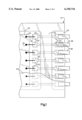
- FIG. 1 is a bottom plan view, somewhat schematic with parts broken away for clarity, of a portion of the package of an integrated circuit chip and chip carrier;
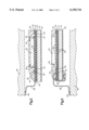
- FIG. 2 is a longitudinal sectional view of the chip and chip carrier of FIG. 1 showing the package mounted to a circuit board;
- FIG. 3 is a longitudinal sectional view of another embodiment of a package according to the present invention mounted to a circuit board;
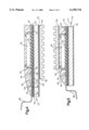
- FIG. 4 is a longitudinal sectional view of another embodiment of the present invention utilizing an additional heat sink
- FIG. 5 is a longitudinal sectional view of another embodiment according to the present invention also utilizing an additional heat sink, but in a different configuration
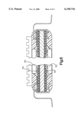
- FIG. 6 is a longitudinal sectional view of an embodiment of the present invention utilizing chips on both sides of the carrier and also utilizing an additional heat sink.
- FIGS. 1 and 2 one embodiment of an integrated circuit (IC) chip package mounted to a circuit board according to the present invention is shown.
- IC integrated circuit
- the package includes a chip carrier designated generally as 10, which includes a metal substrate 12.
- the metal substrate is a copper core 14 having chromium 16 and 18 plated on opposite faces thereof.
- other metals could be used, such as pure copper, invar, copper--invar--copper (C--I--C) and other such materials.
- chromium-plated copper is the preferred material since it is an extremely good electrical conductor and has good heat conducting properties so as to operate as a heat sink.
- the substrate 12 is about 0.025 inch thick, although the thickness can range from about 0.010 inch to about 0.040 inch thick. A substrate thinner than 0.010 inch significantly reduces the effectiveness of the substrate as a heat spreader, and a substrate greater than about 0.040 inch makes the package bulky and heavy and does not provide any significant additional heat dissipation.
- a thin layer of a dielectric material 20 is applied to one face of the substrate 10 over the chromium 16 thereon, which dielectric preferably has a dielectric constant of between about 3.5 and 4.0.
- the preferred dielectric is polyimide.
- the polyimide preferably is applied by spraying which allows for a uniform thin coating to be applied.
- the polyimide can be spin coated.
- Other dielectrics, such as epoxies, polytetrafluoroethylene, etc., can be used; however, polyimide is preferred because it is easily applied, has uniform coating and can be maintained on the surface without substantial defects down to a thickness of about 6 microns, which is the preferred thickness. However, a thickness up to about 20 microns can be used.
- the efficiency of the substrate 12 is about 95% of theoretical efficiency, whereas at 20 microns thickness of the polyimide 20, the efficiency falls off to about 50% theoretical.
- the thickness of about 20 microns is the desired maximum thickness of the dielectric material 20, whereas a thickness of about 6 microns or less is preferred.
- Electrical circuitry is formed on the surface of the dielectric material 20, which electrical circuitry includes chip attachment pads 22, connection pads 24, and circuit traces 26.
- the circuitry is preferably formed by photoresist technology using sputter deposited metal and subtractive etching techniques as is well known in the art.
- the metal is sputter deposited to a thickness of about 6 microns; however, the thickness of the metal can range from about 4 microns to about 8 microns. Metal thinner than about 4 microns can lead to circuit discontinuities, and metal greater than about 8 microns thick inhibits the production of fine circuit features.
- An IC chip 30 is provided which is secured to the surface of the substrate 12 by means of conductive epoxy 32.
- the IC chip 30 has a plurality of I/O contacts 34 which are connected to the chip attach pads 22 by means of wire bond leads 36.
- the connection pads 24 are provided with electrical leads 38.
- a protective coating 42 is applied which can be polyimide. However, there are many other coatings, such as epoxies, which can be used.
- the coating can be patterned, screened or, if photosensitive coatings are used, a photolithographic technique can be used to pattern the coating.
- the protective coating 42 is applied over the circuit traces 26 leaving the chip attachment pads 22 and the connection pads 24 exposed for connection.
- the wire bonds 36 are attached to their respective I/O contacts 34 and chip attach pads 22, preferably by thermosonic bonding.
- the electrical leads 38 are secured to their respective attachment pads 24, preferably by means of solder connections (not shown). Other types of connections, such as conductive epoxy could be used as is well known in the art.
- the entire surface of the substrate 12 is coated with an epoxy encapsulant 44.
- the electrical leads 38 are attached to contacts 46 or circuit board 48.
- the use of the metal substrate 12 provides several advantages over a metalized ceramic substrate.
- One of these is the relative flexibility of the metal substrate 12, thus reducing the propensity for cracking either as a result of thermal excursions or mechanical handling, as compared to a ceramic carrier, especially in the green state.
- Another very significant advantage is the excellent heat conducting properties of the metal substrate 12 which allows heat to be quickly dissipated much more efficiently than with a ceramic substrate.
- the metal substrate provides a floating ground plane for the contacts and circuitry which is especially effective with a thin dielectric layer at the 6 micron level.
- a factor that must be considered is the significant difference in the coefficient of thermal expansions between the IC chip 30 and the carrier 10 because of the metal substrate 12.
- An IC chip formed of silicon has a coefficient of thermal expansion (CTE) in the range of about 3-4 ppm/° C.
- copper has a coefficient of thermal expansion in the range of 18 ppm/° C.
- CTE coefficient of thermal expansion
- a selection of a different material for the substrate 12, such as copper--invar--copper or invar can reduce the mismatch of the CTE's of the chip 30 and the substrate 12.
- FIG. 3 shows another embodiment of the present invention in which flip chip bonding can be utilized to form the package of the carrier and chip.
- an IC chip 52 is provided which is mounted to the chip attach pads 22 by means of solder balls 54.
- a reinforcing epoxy 56 is disposed between the chip 52 and the carrier 12 surrounding the solder balls 54. This reinforcing epoxy assists in preventing damage due to thermal mismatch.
- insulating material 58 is provide around the end of the substrate 12 and on the opposite surface of the substrate 12 so that lead 60 is electrically insulated from the substrate 12. In this case, leads 60 connect the connection pads 24 to the contacts 46 or the circuit board 48.
- FIG. 4 shows how a flip chip 52 can be bonded to the same side of the carrier as a wire bond chip 30.
- FIG. 5 shows another embodiment where an additional heat sink 62 is provided, but in this case the heat sink is secured by conductive epoxy 63 to the top of the epoxy 44 encapsulating the chip.
- FIG. 6 shows an embodiment where chips can be provided on both sides of the chip carrier 10.
- the embodiment is shown utilizing flip chip technology as shown in FIG. 3 for chips on both sides of the substrate.
- wire bond could be used for chips on both sides, or one side could use wire bond technology and the other side flip chip technology.
- heat sink 62 optionally is secured to one side, although if space permits, heat sinks could be provided on both sides.
Abstract
Description
Claims (17)
Priority Applications (12)
| Application Number | Priority Date | Filing Date | Title |
|---|---|---|---|
| US08/783,775 US6150716A (en) | 1995-01-25 | 1997-01-15 | Metal substrate having an IC chip and carrier mounting |
| HU9701377A HUP9701377A3 (en) | 1997-01-15 | 1997-08-11 | Case and method for mouting an ic chip onto a carrier board or similar |
| KR1019970052339A KR100259412B1 (en) | 1997-01-15 | 1997-10-13 | Metallic substrate having ic chip and supporting structure |
| CN97125492A CN1132243C (en) | 1997-01-15 | 1997-12-12 | Metal substrate having IC chip and carrier mounting |
| MYPI97006030A MY127468A (en) | 1997-01-15 | 1997-12-12 | Metal substrate having an ic chip and carrier mounting |
| SG1997004458A SG60170A1 (en) | 1997-01-15 | 1997-12-15 | Metal substrate having an ic chip and carrier mounting |
| TW087100113A TW473887B (en) | 1997-01-15 | 1998-01-06 | Metal substrate having an IC chip and carrier mounting |
| CZ9834A CZ3498A3 (en) | 1997-01-15 | 1998-01-07 | Metallic substrate having ic chip and supporting structure |
| PL98324177A PL324177A1 (en) | 1997-01-15 | 1998-01-08 | Method of mounting and integrated circuit on its associated circuit board and mounting unit therefor |
| JP10003024A JP2903013B2 (en) | 1997-01-15 | 1998-01-09 | Circuit package including metal substrate and mounting method |
| RU98101113/28A RU2191445C2 (en) | 1997-01-15 | 1998-01-14 | Package to mount chip in integrated circuit and process of its assembly |
| US09/426,577 US6131278A (en) | 1995-01-25 | 1999-10-25 | Metal substrate having an IC chip and carrier mounting |
Applications Claiming Priority (2)
| Application Number | Priority Date | Filing Date | Title |
|---|---|---|---|
| US08/378,347 US5616958A (en) | 1995-01-25 | 1995-01-25 | Electronic package |
| US08/783,775 US6150716A (en) | 1995-01-25 | 1997-01-15 | Metal substrate having an IC chip and carrier mounting |
Related Parent Applications (1)
| Application Number | Title | Priority Date | Filing Date |
|---|---|---|---|
| US08/378,347 Continuation-In-Part US5616958A (en) | 1995-01-25 | 1995-01-25 | Electronic package |
Related Child Applications (1)
| Application Number | Title | Priority Date | Filing Date |
|---|---|---|---|
| US09/426,577 Division US6131278A (en) | 1995-01-25 | 1999-10-25 | Metal substrate having an IC chip and carrier mounting |
Publications (1)
| Publication Number | Publication Date |
|---|---|
| US6150716A true US6150716A (en) | 2000-11-21 |
Family
ID=27008181
Family Applications (2)
| Application Number | Title | Priority Date | Filing Date |
|---|---|---|---|
| US08/783,775 Expired - Fee Related US6150716A (en) | 1995-01-25 | 1997-01-15 | Metal substrate having an IC chip and carrier mounting |
| US09/426,577 Expired - Fee Related US6131278A (en) | 1995-01-25 | 1999-10-25 | Metal substrate having an IC chip and carrier mounting |
Family Applications After (1)
| Application Number | Title | Priority Date | Filing Date |
|---|---|---|---|
| US09/426,577 Expired - Fee Related US6131278A (en) | 1995-01-25 | 1999-10-25 | Metal substrate having an IC chip and carrier mounting |
Country Status (1)
| Country | Link |
|---|---|
| US (2) | US6150716A (en) |
Cited By (17)
| Publication number | Priority date | Publication date | Assignee | Title |
|---|---|---|---|---|
| US6339247B1 (en) * | 1999-01-20 | 2002-01-15 | Citizen Watch Co., Ltd. | Structure for mounting a semiconductor device on a liquid crystal display, and semiconductor device |
| US6531333B2 (en) * | 2000-04-05 | 2003-03-11 | Hong-Ming Lin | Chip photoelectric sensor assembly and method for making same |
| US6858942B1 (en) * | 1999-12-08 | 2005-02-22 | Altera Corporation | Semiconductor package with improved thermal cycling performance, and method of forming same |
| US20060043577A1 (en) * | 2004-08-31 | 2006-03-02 | Chih-An Yang | Structure and process of semiconductor package with an exposed heatsink |
| WO2006072176A1 (en) * | 2005-01-05 | 2006-07-13 | Tir Systems Ltd. | Thermally and electrically conductive apparatus |
| KR100716870B1 (en) * | 2001-04-20 | 2007-05-09 | 앰코 테크놀로지 코리아 주식회사 | Semiconductor package and its manufacturing method |
| US8119446B2 (en) | 2001-12-31 | 2012-02-21 | Megica Corporation | Integrated chip package structure using metal substrate and method of manufacturing the same |
| US8471361B2 (en) | 2001-12-31 | 2013-06-25 | Megica Corporation | Integrated chip package structure using organic substrate and method of manufacturing the same |
| US8492870B2 (en) | 2002-01-19 | 2013-07-23 | Megica Corporation | Semiconductor package with interconnect layers |
| US8535976B2 (en) | 2001-12-31 | 2013-09-17 | Megica Corporation | Method for fabricating chip package with die and substrate |
| US9030029B2 (en) | 2001-12-31 | 2015-05-12 | Qualcomm Incorporated | Chip package with die and substrate |
| US20160027757A1 (en) * | 2012-09-28 | 2016-01-28 | Intel Corporation | Bumpless build-up layer package including an integrated heat spreader |
| US9666549B2 (en) | 2013-09-25 | 2017-05-30 | Intel Corporation | Methods for solder for through-mold interconnect |
| US9741664B2 (en) | 2013-09-25 | 2017-08-22 | Intel Corporation | High density substrate interconnect formed through inkjet printing |
| US9814371B2 (en) | 2012-03-30 | 2017-11-14 | Fujikura Ltd. | Imaging module, lens-attached imaging module, endoscope, method of manufacturing imaging module, and flexible wiring substrate formation apparatus |
| US10199346B2 (en) | 2012-12-06 | 2019-02-05 | Intel Corporation | High density substrate routing in package |
| US10366951B2 (en) | 2012-09-28 | 2019-07-30 | Intel Corporation | Localized high density substrate routing |
Families Citing this family (4)
| Publication number | Priority date | Publication date | Assignee | Title |
|---|---|---|---|---|
| US7019410B1 (en) * | 1999-12-21 | 2006-03-28 | Micron Technology, Inc. | Die attach material for TBGA or flexible circuitry |
| US6867491B2 (en) * | 2001-12-19 | 2005-03-15 | Intel Corporation | Metal core integrated circuit package with electrically isolated regions and associated methods |
| US20180275571A1 (en) * | 2015-09-17 | 2018-09-27 | Ntn Corporation | Manufacturing method for sliding member for fixing device |
| US10586716B2 (en) * | 2017-06-09 | 2020-03-10 | Advanced Semiconductor Engineering, Inc. | Semiconductor device package |
Citations (18)
| Publication number | Priority date | Publication date | Assignee | Title |
|---|---|---|---|---|
| US3781596A (en) * | 1972-07-07 | 1973-12-25 | R Galli | Semiconductor chip carriers and strips thereof |
| US3981691A (en) * | 1974-07-01 | 1976-09-21 | Minnesota Mining And Manufacturing Company | Metal-clad dielectric sheeting having an improved bond between the metal and dielectric layers |
| US4092697A (en) * | 1976-12-06 | 1978-05-30 | International Business Machines Corporation | Heat transfer mechanism for integrated circuit package |
| US4711804A (en) * | 1986-07-02 | 1987-12-08 | General Electric Company | Circuit board construction |
| US4882454A (en) * | 1988-02-12 | 1989-11-21 | Texas Instruments Incorporated | Thermal interface for a printed wiring board |
| JPH02131935A (en) * | 1988-11-14 | 1990-05-21 | Mitsui Toatsu Chem Inc | Flexible copper-clad board |
| US5038132A (en) * | 1989-12-22 | 1991-08-06 | Texas Instruments Incorporated | Dual function circuit board, a resistor element therefor, and a circuit embodying the element |
| US5044074A (en) * | 1988-01-08 | 1991-09-03 | Siemens Aktiengesellschaft | Method for manufacturing metal core printed circuit boards |
| US5168926A (en) * | 1991-09-25 | 1992-12-08 | Intel Corporation | Heat sink design integrating interface material |
| US5173844A (en) * | 1987-05-19 | 1992-12-22 | Mitsubishi Denki Kabushiki Kaisha | Integrated circuit device having a metal substrate |
| US5194933A (en) * | 1990-10-05 | 1993-03-16 | Fuji Electric Co., Ltd. | Semiconductor device using insulation coated metal substrate |
| US5320919A (en) * | 1990-06-08 | 1994-06-14 | Sumitomo Bakelite Company Limited | Copper foil for inner layer circuit of multi-layered printed circuit board, method of producing the same and multi-layered printed circuit board having the same |
| US5390082A (en) * | 1992-07-06 | 1995-02-14 | International Business Machines, Corp. | Chip carrier with protective coating for circuitized surface |
| US5583378A (en) * | 1994-05-16 | 1996-12-10 | Amkor Electronics, Inc. | Ball grid array integrated circuit package with thermal conductor |
| US5610442A (en) * | 1995-03-27 | 1997-03-11 | Lsi Logic Corporation | Semiconductor device package fabrication method and apparatus |
| US5616958A (en) * | 1995-01-25 | 1997-04-01 | International Business Machines Corporation | Electronic package |
| US5629835A (en) * | 1994-07-19 | 1997-05-13 | Olin Corporation | Metal ball grid array package with improved thermal conductivity |
| US5635762A (en) * | 1993-05-18 | 1997-06-03 | U.S. Philips Corporation | Flip chip semiconductor device with dual purpose metallized ground conductor |
Family Cites Families (6)
| Publication number | Priority date | Publication date | Assignee | Title |
|---|---|---|---|---|
| US4801765A (en) * | 1986-01-06 | 1989-01-31 | American Telephone And Telegraph Company, At&T Bell Laboratories | Electronic component package using multi-level lead frames |
| US5206986A (en) * | 1989-08-11 | 1993-05-04 | Fujitsu Limited | Method of producing an electronic circuit package |
| US5249354A (en) * | 1991-09-25 | 1993-10-05 | American Telephone & Telegraph Co. | Method of making electronic component packages |
| US5359768A (en) * | 1992-07-30 | 1994-11-01 | Intel Corporation | Method for mounting very small integrated circuit package on PCB |
| US5422313A (en) * | 1994-05-03 | 1995-06-06 | Texas Instruments Incorporated | Integrated circuit device and manufacturing method using photoresist lead covering |
| US5615475A (en) * | 1995-01-30 | 1997-04-01 | Staktek Corporation | Method of manufacturing an integrated package having a pair of die on a common lead frame |
-
1997
- 1997-01-15 US US08/783,775 patent/US6150716A/en not_active Expired - Fee Related
-
1999
- 1999-10-25 US US09/426,577 patent/US6131278A/en not_active Expired - Fee Related
Patent Citations (18)
| Publication number | Priority date | Publication date | Assignee | Title |
|---|---|---|---|---|
| US3781596A (en) * | 1972-07-07 | 1973-12-25 | R Galli | Semiconductor chip carriers and strips thereof |
| US3981691A (en) * | 1974-07-01 | 1976-09-21 | Minnesota Mining And Manufacturing Company | Metal-clad dielectric sheeting having an improved bond between the metal and dielectric layers |
| US4092697A (en) * | 1976-12-06 | 1978-05-30 | International Business Machines Corporation | Heat transfer mechanism for integrated circuit package |
| US4711804A (en) * | 1986-07-02 | 1987-12-08 | General Electric Company | Circuit board construction |
| US5173844A (en) * | 1987-05-19 | 1992-12-22 | Mitsubishi Denki Kabushiki Kaisha | Integrated circuit device having a metal substrate |
| US5044074A (en) * | 1988-01-08 | 1991-09-03 | Siemens Aktiengesellschaft | Method for manufacturing metal core printed circuit boards |
| US4882454A (en) * | 1988-02-12 | 1989-11-21 | Texas Instruments Incorporated | Thermal interface for a printed wiring board |
| JPH02131935A (en) * | 1988-11-14 | 1990-05-21 | Mitsui Toatsu Chem Inc | Flexible copper-clad board |
| US5038132A (en) * | 1989-12-22 | 1991-08-06 | Texas Instruments Incorporated | Dual function circuit board, a resistor element therefor, and a circuit embodying the element |
| US5320919A (en) * | 1990-06-08 | 1994-06-14 | Sumitomo Bakelite Company Limited | Copper foil for inner layer circuit of multi-layered printed circuit board, method of producing the same and multi-layered printed circuit board having the same |
| US5194933A (en) * | 1990-10-05 | 1993-03-16 | Fuji Electric Co., Ltd. | Semiconductor device using insulation coated metal substrate |
| US5168926A (en) * | 1991-09-25 | 1992-12-08 | Intel Corporation | Heat sink design integrating interface material |
| US5390082A (en) * | 1992-07-06 | 1995-02-14 | International Business Machines, Corp. | Chip carrier with protective coating for circuitized surface |
| US5635762A (en) * | 1993-05-18 | 1997-06-03 | U.S. Philips Corporation | Flip chip semiconductor device with dual purpose metallized ground conductor |
| US5583378A (en) * | 1994-05-16 | 1996-12-10 | Amkor Electronics, Inc. | Ball grid array integrated circuit package with thermal conductor |
| US5629835A (en) * | 1994-07-19 | 1997-05-13 | Olin Corporation | Metal ball grid array package with improved thermal conductivity |
| US5616958A (en) * | 1995-01-25 | 1997-04-01 | International Business Machines Corporation | Electronic package |
| US5610442A (en) * | 1995-03-27 | 1997-03-11 | Lsi Logic Corporation | Semiconductor device package fabrication method and apparatus |
Non-Patent Citations (6)
| Title |
|---|
| "Connected Ground and Floating Plane Package Design and Electrical Analysis," M.K. Kerr, S.P. Moore and W.F. Lawson, 44th Electronic Components and Technology Conference, May, 1994, pp. 971-977. |
| Anonymous, "Cable Attached Surface Mount Package," Research Disclosure, Oct. 1989, No. 306 (30680). |
| Anonymous, Cable Attached Surface Mount Package, Research Disclosure, Oct. 1989, No. 306 (30680). * |
| Connected Ground and Floating Plane Package Design and Electrical Analysis, M.K. Kerr, S.P. Moore and W.F. Lawson, 44th Electronic Components and Technology Conference, May, 1994, pp. 971 977. * |
| U.S. Statutory Invention Registration No. H498 Published Jul. 5, 1988. Keller et al. * |
| U.S. Statutory Invention Registration No. H498--Published Jul. 5, 1988. Keller et al. |
Cited By (27)
| Publication number | Priority date | Publication date | Assignee | Title |
|---|---|---|---|---|
| US6339247B1 (en) * | 1999-01-20 | 2002-01-15 | Citizen Watch Co., Ltd. | Structure for mounting a semiconductor device on a liquid crystal display, and semiconductor device |
| US6858942B1 (en) * | 1999-12-08 | 2005-02-22 | Altera Corporation | Semiconductor package with improved thermal cycling performance, and method of forming same |
| US6531333B2 (en) * | 2000-04-05 | 2003-03-11 | Hong-Ming Lin | Chip photoelectric sensor assembly and method for making same |
| KR100716870B1 (en) * | 2001-04-20 | 2007-05-09 | 앰코 테크놀로지 코리아 주식회사 | Semiconductor package and its manufacturing method |
| US9030029B2 (en) | 2001-12-31 | 2015-05-12 | Qualcomm Incorporated | Chip package with die and substrate |
| US9136246B2 (en) | 2001-12-31 | 2015-09-15 | Qualcomm Incorporated | Integrated chip package structure using silicon substrate and method of manufacturing the same |
| US8119446B2 (en) | 2001-12-31 | 2012-02-21 | Megica Corporation | Integrated chip package structure using metal substrate and method of manufacturing the same |
| US8471361B2 (en) | 2001-12-31 | 2013-06-25 | Megica Corporation | Integrated chip package structure using organic substrate and method of manufacturing the same |
| US8535976B2 (en) | 2001-12-31 | 2013-09-17 | Megica Corporation | Method for fabricating chip package with die and substrate |
| US8835221B2 (en) | 2001-12-31 | 2014-09-16 | Qualcomm Incorporated | Integrated chip package structure using ceramic substrate and method of manufacturing the same |
| US8492870B2 (en) | 2002-01-19 | 2013-07-23 | Megica Corporation | Semiconductor package with interconnect layers |
| US20060043577A1 (en) * | 2004-08-31 | 2006-03-02 | Chih-An Yang | Structure and process of semiconductor package with an exposed heatsink |
| US20080239675A1 (en) * | 2005-01-05 | 2008-10-02 | Tir Systems Ltd. | Thermally and Electrically Conductive Apparatus |
| US9111822B2 (en) | 2005-01-05 | 2015-08-18 | Koninklijke Philips N. V. | Thermally and electrically conductive apparatus |
| WO2006072176A1 (en) * | 2005-01-05 | 2006-07-13 | Tir Systems Ltd. | Thermally and electrically conductive apparatus |
| US9814371B2 (en) | 2012-03-30 | 2017-11-14 | Fujikura Ltd. | Imaging module, lens-attached imaging module, endoscope, method of manufacturing imaging module, and flexible wiring substrate formation apparatus |
| US9520376B2 (en) * | 2012-09-28 | 2016-12-13 | Intel Corporation | Bumpless build-up layer package including an integrated heat spreader |
| US20160027757A1 (en) * | 2012-09-28 | 2016-01-28 | Intel Corporation | Bumpless build-up layer package including an integrated heat spreader |
| US10366951B2 (en) | 2012-09-28 | 2019-07-30 | Intel Corporation | Localized high density substrate routing |
| US10796988B2 (en) | 2012-09-28 | 2020-10-06 | Intel Corporation | Localized high density substrate routing |
| US11515248B2 (en) | 2012-09-28 | 2022-11-29 | Intel Corporation | Localized high density substrate routing |
| US10199346B2 (en) | 2012-12-06 | 2019-02-05 | Intel Corporation | High density substrate routing in package |
| US10438915B2 (en) | 2012-12-06 | 2019-10-08 | Intel Corporation | High density substrate routing in package |
| US10861815B2 (en) | 2012-12-06 | 2020-12-08 | Intel Corporation | High density substrate routing in package |
| US11251150B2 (en) | 2012-12-06 | 2022-02-15 | Intel Corporation | High density substrate routing in package |
| US9666549B2 (en) | 2013-09-25 | 2017-05-30 | Intel Corporation | Methods for solder for through-mold interconnect |
| US9741664B2 (en) | 2013-09-25 | 2017-08-22 | Intel Corporation | High density substrate interconnect formed through inkjet printing |
Also Published As
| Publication number | Publication date |
|---|---|
| US6131278A (en) | 2000-10-17 |
Similar Documents
| Publication | Publication Date | Title |
|---|---|---|
| US6150716A (en) | Metal substrate having an IC chip and carrier mounting | |
| US5578525A (en) | Semiconductor device and a fabrication process thereof | |
| US5376588A (en) | Method for making high pin count package for semiconductor device | |
| EP0797253B1 (en) | Chip carrier and semiconductor device using the same | |
| US5753974A (en) | Electronic device assembly | |
| US7687896B2 (en) | Semiconductor device having a stacked chip structure | |
| US7565737B2 (en) | Manufacturing method of package substrate | |
| JP3728847B2 (en) | Multi-chip module and manufacturing method thereof | |
| US5966803A (en) | Ball grid array having no through holes or via interconnections | |
| JP3312611B2 (en) | Film carrier type semiconductor device | |
| JPH0573079B2 (en) | ||
| KR100259412B1 (en) | Metallic substrate having ic chip and supporting structure | |
| US6509642B1 (en) | Integrated circuit package | |
| US20060197233A1 (en) | Die attach material for TBGA or flexible circuitry | |
| WO1999013509A1 (en) | Semiconductor device | |
| KR100203932B1 (en) | BGA package having thermal emissive substrate attached to chip | |
| GB2293918A (en) | Electronic circuit packaging | |
| KR100218633B1 (en) | Ball grid array package having a carrier frame | |
| KR20000044989A (en) | Multi chip ball grid array package | |
| KR100525452B1 (en) | Semiconductor package & PCB mounted with the same | |
| JPS61150251A (en) | Semiconductor device | |
| KR19980025878A (en) | Ball grid array package with a heat sink attached to the chip | |
| KR19980025868A (en) | Metal Ball Grid Array Package | |
| JPS6185834A (en) | Semiconductor device | |
| KR19980021720A (en) | Power transistor package with insulated metal substrate |
Legal Events
| Date | Code | Title | Description |
|---|---|---|---|
| AS | Assignment |
Owner name: INTERNATIONAL BUSINESS MACHINES CORPORATION, NEW Y Free format text: ASSIGNMENT OF ASSIGNORS INTEREST;ASSIGNORS:MACQUARRIE, STEPHEN WESLEY;STORR, WAYNE RUSSELL;WILSON, JAMES WARREN;REEL/FRAME:008480/0721;SIGNING DATES FROM 19970108 TO 19970109 |
|
| FEPP | Fee payment procedure |
Free format text: PAYOR NUMBER ASSIGNED (ORIGINAL EVENT CODE: ASPN); ENTITY STATUS OF PATENT OWNER: LARGE ENTITY |
|
| FEPP | Fee payment procedure |
Free format text: PAYER NUMBER DE-ASSIGNED (ORIGINAL EVENT CODE: RMPN); ENTITY STATUS OF PATENT OWNER: LARGE ENTITY Free format text: PAYOR NUMBER ASSIGNED (ORIGINAL EVENT CODE: ASPN); ENTITY STATUS OF PATENT OWNER: LARGE ENTITY |
|
| FPAY | Fee payment |
Year of fee payment: 4 |
|
| REMI | Maintenance fee reminder mailed | ||
| LAPS | Lapse for failure to pay maintenance fees | ||
| STCH | Information on status: patent discontinuation |
Free format text: PATENT EXPIRED DUE TO NONPAYMENT OF MAINTENANCE FEES UNDER 37 CFR 1.362 |
|
| FP | Lapsed due to failure to pay maintenance fee |
Effective date: 20081121 |