US6150844A - High voltage tolerance output stage - Google Patents
High voltage tolerance output stage Download PDFInfo
- Publication number
- US6150844A US6150844A US08/898,811 US89881197A US6150844A US 6150844 A US6150844 A US 6150844A US 89881197 A US89881197 A US 89881197A US 6150844 A US6150844 A US 6150844A
- Authority
- US
- United States
- Prior art keywords
- output
- transistor
- terminal
- pull
- switch
- Prior art date
- Legal status (The legal status is an assumption and is not a legal conclusion. Google has not performed a legal analysis and makes no representation as to the accuracy of the status listed.)
- Expired - Lifetime
Links
Images
Classifications
-
- H—ELECTRICITY
- H03—ELECTRONIC CIRCUITRY
- H03K—PULSE TECHNIQUE
- H03K19/00—Logic circuits, i.e. having at least two inputs acting on one output; Inverting circuits
- H03K19/003—Modifications for increasing the reliability for protection
- H03K19/00315—Modifications for increasing the reliability for protection in field-effect transistor circuits
-
- H—ELECTRICITY
- H03—ELECTRONIC CIRCUITRY
- H03K—PULSE TECHNIQUE
- H03K19/00—Logic circuits, i.e. having at least two inputs acting on one output; Inverting circuits
- H03K19/003—Modifications for increasing the reliability for protection
- H03K19/00369—Modifications for compensating variations of temperature, supply voltage or other physical parameters
- H03K19/00384—Modifications for compensating variations of temperature, supply voltage or other physical parameters in field effect transistor circuits
Definitions
- the present invention relates to an output stage for high voltage tolerance electronic circuits. More particularly, the present invention relates to an output stage for a high voltage tolerance electronic circuit, the output stage having a protection device that protects against undesired starting up, and includes an output buffer made up of a complementary pair of transistors having a P-channel MOS pull-up transistor and an N-channel MOS pull-down transistor with these transistors being connected mutually to form an output terminal of the stage.
- problems in the use and management of resources common to both types of devices For example, problems occur when a data bus is shared by different digital systems incorporating electronic circuits operating at 3 V and electronic circuits operating at 5 V.
- a logical control unit e.g., a CPU (Central Processing Unit), which emits enable and disable signals for the various circuits sharing the data bus.
- a CPU Central Processing Unit
- each circuit has control inputs and has a final output stage incorporating an output buffer made up essentially of a complementary pair of pull-up and pull-down circuits connected to the data bus.
- the CPU acts on the OE# (Output Enable) or CE (Chip Enable) signal inputs of the unused circuits to force the corresponding output buffers into an off state, or a "tristate.”
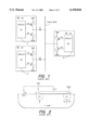
- FIG. 1 A diagram of this situation is shown in FIG. 1 illustrating a group of electronic circuits sharing the same data bus even though operating with different supply voltages.
- FIG. 1 also shows the bias voltages applied to the various output buffers when one of the circuits (in the example, the one with high power supply) is using the data bus.
- each pull-up transistor of an output buffer that is turned off has its gate terminal and body terminal powered by a voltage Vcc of 3 V.
- Vcc value 3V+min [
- the PMOS transistor is turned on. Otherwise, the NMOS transistors is turned on.
- FIG. 2 shows an enlarged vertical cross section of the internal structure of a P-channel MOS transistor provided in an N well.
- the symbols S, G and D indicate respectively the terminals of the source, gate and drain regions.
- B indicates the body or bulk terminal of the transistor.
- a conventional solution consists of providing a diode connected in parallel to the P-channel pull-up transistor of the output buffer. This diode is directly biased like the drain-bulk junction but turns on first because of an expected lower threshold voltage.
- a technical problem underlying the present invention is to conceive an electronic circuit output stage having high voltage tolerance and also having structural and functional characteristics allowing protection against undesired turning on which would also make current consumption virtually null when the output buffer of the stage is off.
- An embodiment of the invention is directed to an output stage for an electronic circuit with a high voltage tolerance.
- the output stage includes an output buffer including a complimentary transistor pair having a pull-up P-channel MOS transistor and a pull-down N-channel MOS transistor with the transistors being connected to form an output stage output terminal.
- the pull-up P-channel MOS transistor has a control terminal.
- the output stage further includes a switch having a switch input coupled to the output stage output terminal, and a switch output coupled to the control terminal of the pull-up P-channel MOS transistor to drive the output stage into a tristate condition.
- FIG. 1 shows a diagrammatic view of a group of electronic circuits having respective output stages connected to the same data bus
- FIG. 2 shows a diagrammatic view of an enlarged vertical cross section of the internal structure of a P-channel MOS transistor provided in an N well of a semiconductor substrate;
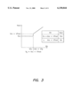
- FIG. 3 shows a voltage-voltage diagram representative of the transfer function of a component of the output stage in accordance with the present invention
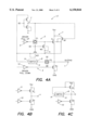
- FIGS. 4A, 4B and 4C show respective diagrammatic views of an output stage provided in accordance with the present invention and in different operating conditions
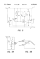
- FIG. 5 shows a diagrammatic view of a circuit detail of a detail of the stage of FIG. 4A
- FIG. 6A shows a diagrammatic view of a detail of the circuit of FIG. 5.
- FIG. 6B shows a chart of voltage signals present in the circuit of FIG. 5.
- reference number 1 indicates as a whole and schematically a final output stage provided in accordance with the present invention for an electronic circuit 2.
- circuit 2 is represented only partially and by way of indication in FIG. 4A because it may be of varying type such as, e.g., a memory device, a reading circuit or some other circuit.
- Circuit 2 has at least one enable input, an operational portion whose operation is interlocked with the signal present on that input, and a final output stage which in our case corresponds to the stage 1.
- the stage 1 includes a CMOS complementary transistor pair made up of a first P-channel pull-up transistor Pu connected in series with a second N-channel pull-down transistor Nu. These two transistors Pu and Nu are connected between a first reference supply voltage Vcc and a second reference voltage, e.g., a signal ground.
- the point of connection between the transistors Pu and Nu corresponds to the output terminal U of the stage 1.
- the circuit 2 calls for a drive portion 3 of the pull-up transistor Pu and a like portion 4 for driving the pull-down transistor Nu.
- the first 3 of these portions includes essentially an inverter 5 having its output coupled to the control terminal of the transistor Pu through a pass-transistor P1.
- the second portion 4 calls for a direct connection between the output of an inverter 10 and the control terminal of the pull-down transistor Nu.
- a pass-transistor is virtually an enable circuit element having two inputs on which are applied mutually complementary signals.
- One of the inputs of the pass-transistor P1 is connected to the output of a CMOS inverter 7 made up of a complementary transistor pair receiving in parallel on respective control terminals the same enable signal OE.
- the other input of the pass-transistor P1 receives this signal OE directly.
- the stage 1 is equipped with a protection device against undesired turning on.
- This protection device includes a switch 6 having an input 8 and an output 9.
- the input 8 of the switch 6 is coupled to the output node U through a pass-transistor P2 receiving the signals OE and OE.
- the output 9 of the switch 6 is connected to power the inverter 7.
- the switch 6 has a threshold and switching voltage Vs which is appropriately selected to be within the following range:
- the voltage Vs was chosen equal to a Vcc+Vtnat, where Vtnat is the threshold voltage of a natural transistor and its value is less than min [
- the structure of the stage 1 in accordance with the present invention further includes a first P-channel MOS transistor M1 having its control terminal coupled downstream of the output of the inverter 7.
- the source terminal of the transistor M1 is connected to the reference supply voltage Vcc while the drain terminal and the body terminal of the transistor M1 are coupled to the control terminal of the pull-up transistor Pu through a MOS transistor M2.
- a second M2 and a third M3 transistors are disposed between the control terminal of the pull-up transistor Pu and the output 9 of the switch 6.
- the signal OE On the control terminal of both these transistors M2 and M3 is applied the signal OE. The interconnection point between them is indicated as node A and is connected to the drain terminal of the first transistor M1.
- stage 1 in accordance with the present invention and of the circuitry associated therewith.
- the electronic circuit 2 When the electronic circuit 2 is active to perform, e.g., reading of the information transmitted on a data bus, the corresponding output buffer is turned on.
- the enable signal OE has high logical value and the transistors M2 and M3 are off. Under these conditions the pass-transistor P2 is also off and the switch 6 is deactivated.
- the transistor M1 and the pass-transistor P1 are on and the circuit shown in FIG. 4A is equivalent to an operational structure as shown in FIG. 4B.
- the respective inverters 5 and 10 directly drive the control terminals of the pull-up Pu and pull-down Nu.
- transistors M2 and M3 are turned on as is the pass-transistor P2.
- the transistor M1 and the pass-transistor P1 are turned off.
- FIG. 4C diagrams this operational situation.
- the output 9 of the switch 6 is directly connected to the control terminal and the bulk of the pull-up transistor Pu.
- the stage in accordance with the present invention has the special characteristic of allowing direct connection between the output of the switch 6 and the gate and bulk regions of the output buffer pull-up. This connection is active only when the output buffer is in tristate.
- FIG. 3 shows a transfer function Vin/Vout representing the output voltage Vout of the switch 6 for variations in the voltage Vin applied at input.
- the switch 6 is capable of comparing the voltage present on the buffer output U with its own threshold voltage Vs and supplying at output the greater of the two values.
- the result of this behavior is given in the graph shown in FIG. 3 by a broken line corresponding to the values of the following table.
- the threshold voltage Vs for switching of the switch 6 was chosen in the range defined by the (1) to avoid consumption of the active device.
- the switch 6 has an input terminal 8 and an output terminal 9.
- the input terminal is connected to the control terminal G1 of a P-channel MOS transistor M10 inserted between the reference supply voltage Vcc and the output terminal 9.
- a second P-channel MOS transistor M20 is in turn connected between the reference supply voltage Vcc and the output terminal 9 of the switch 6.
- the control terminal G2 of the second transistor M20 is connected to the input 8 through a transistor Dp1 in diode configuration and biased directly to said control terminal G2.
- a transistor pair Dp2 and Dnat in mutual series is connected in parallel with the above mentioned diode Dp1 but with opposite bias.
- a third P-channel MOS transistor M30 is inserted in turn between the input 8 and the output 9. This third transistor M30 has its control terminal G3 connected to a capacitive divider 11.
- the divider 11 includes a capacitor C2 connected to a capacitor C1 between the power supply reference and the second ground reference.
- the point of interconnection between the capacitors C2 and C1 is connected to the terminal G3.
- a transistor Dnat in diode configuration is connected in parallel with the capacitor C2 with bias towards the supply voltage Vcc.
- the structure of the switch 6 is completed by a fourth P-channel MOS transistor M40 having its drain terminal connected to the input 8, its source terminal connected to the control terminal G2 of the second transistor M20 and its bulk terminal connected to the output 9.
- control terminal G4 of the fourth transistor M40 is connected to the same capacitive divider 11.
- the transistor M10 is on and holds the output voltage Vout at the value of the supply voltage Vcc.
- the series connection of the transistors Dp2 and Dnat causes a voltage drop on the terminal G2 which reaches a potential voltage Vg2 equal to Vin-(
- the second transistor M20 is accordingly turned on until the input voltage Vin reaches the value Vcc+Vtnat.
- the output terminal 9 is thus held at Vcc.
- the transistors M30 and M40 turn on when on their drain terminals, connected to the input 8, the voltage Vin reaches the value Vcc-Vtnat+
- Vtnat in such a manner as to determine the simultaneous turning on of the third transistor M30 and turning off of the second transistor M20.
- the value of Vin at which the switching takes place corresponds exactly to the threshold voltage Vs defined above.
- MOS transistor Dp2 allows lowering the potential on the terminal G2 of the second transistor M2 in the falling phase of the input voltage Vin.
- the output stage in accordance with the present invention achieves important advantages with respect to the prior art.
- the first of these advantages is permitting reaching of the full 5 V level on the bus side when the high voltage device is active and thus reducing to virtually zero consumption of the electronic circuits with high power supply connected to the data bus and made active when the low power supply circuits are deactivated.
- FIGS. 6A and 6B discuss the answer of the present invention to this variation in the power supply.
- the switch 6 functions correctly if the control terminal of the third transistor M30 manages to follow the value of the supply voltage Vcc in the above mentioned interval, unless there is a voltage drop equal to the threshold of a natural MOS.
- the capacitive divider 11 was especially provided for this purpose.
- the capacitor C1 is charged by the MOS in diode configuration Dnat and thus the output voltage Vout moves to Vcc-Vtnat.
- the two capacitors C1 and C2 must be sized in such a manner that the voltage to which their common node would move in the absence of the diode Dnat would be less than Vcc-Vtnat.
- Vcc*C2/(C1+C2) must be less than Vcc-Vtnat and the output voltage Vout will be constrained to a minimum value equal to Vcc-Vtnat.
- the output stage in accordance with the present invention accordingly functions correctly even with variations in the supply voltage Vcc.
Landscapes
- Physics & Mathematics (AREA)
- Engineering & Computer Science (AREA)
- Computer Hardware Design (AREA)
- Computing Systems (AREA)
- General Engineering & Computer Science (AREA)
- Mathematical Physics (AREA)
- Logic Circuits (AREA)
Abstract
Description
Vcc≦Vs≦Vcc+min [|Vthp|, Vγ](1)
              TABLE 1
______________________________________
Buffer
      OE    M1       M2   M3     P1   P2     SW6
______________________________________
ON    1     ON       OFF  OFF    ON   OFF    Deact
  OFF 0 OFF ON ON OFF ON Active
______________________________________
              TABLE 2
______________________________________
Vin                     Vout
  Vin ≦ Vcc + Vtnat Vcc
  Vin ≧ Vcc + Vtnat Vin
______________________________________
              TABLE 3
______________________________________
Vin               M10    M20    M30  M40  Vout
______________________________________
0 to Vcc - Vnat   ON     ON     OFF  OFF  Vcc
  Vcc - | Vtp | to Vcc - Vnat + Vtp OFF ON OFF OFF Vcc
                                           ≧Vcc - Vnat + |
                                           Vtp | OFF OFF ON ON
                                          Vin
______________________________________
Claims (14)
Applications Claiming Priority (2)
| Application Number | Priority Date | Filing Date | Title |
|---|---|---|---|
| EP96830413A EP0821484B1 (en) | 1996-07-24 | 1996-07-24 | High voltage tolerance output stage |
| EP96830413 | 1996-07-24 |
Publications (1)
| Publication Number | Publication Date |
|---|---|
| US6150844A true US6150844A (en) | 2000-11-21 |
Family
ID=8225971
Family Applications (1)
| Application Number | Title | Priority Date | Filing Date |
|---|---|---|---|
| US08/898,811 Expired - Lifetime US6150844A (en) | 1996-07-24 | 1997-07-23 | High voltage tolerance output stage |
Country Status (3)
| Country | Link |
|---|---|
| US (1) | US6150844A (en) |
| EP (1) | EP0821484B1 (en) |
| DE (1) | DE69624230T2 (en) |
Cited By (3)
| Publication number | Priority date | Publication date | Assignee | Title |
|---|---|---|---|---|
| US6268759B1 (en) * | 1999-11-23 | 2001-07-31 | Texas Instruments Incorporated | Low-power 5-volt input/output tolerant circuit with power-down control for a low voltage CMOS crossbar switch |
| US20030161943A1 (en) * | 1996-12-30 | 2003-08-28 | Applied Materials, Inc. | Fully planarized dual damascene metallization using copper line interconnect and selective CVD aluminum plug |
| US20060044015A1 (en) * | 2004-08-26 | 2006-03-02 | Chao-Cheng Lee | High voltage tolerance output stage |
Families Citing this family (1)
| Publication number | Priority date | Publication date | Assignee | Title |
|---|---|---|---|---|
| GB2374475B (en) * | 2000-12-15 | 2005-05-11 | Micron Technology Inc | Input-output buffer circuit and method for avoiding inadvertent conduction of a pull-up transistor |
Citations (7)
| Publication number | Priority date | Publication date | Assignee | Title |
|---|---|---|---|---|
| EP0621692A2 (en) * | 1993-04-19 | 1994-10-26 | Koninklijke Philips Electronics N.V. | Overvoltage protection circuitry |
| US5451889A (en) * | 1994-03-14 | 1995-09-19 | Motorola, Inc. | CMOS output driver which can tolerate an output voltage greater than the supply voltage without latchup or increased leakage current |
| US5512844A (en) * | 1994-07-13 | 1996-04-30 | Matsushita Electric Industrial Co., Ltd. | Output circuit with high output voltage protection means |
| US5543733A (en) * | 1995-06-26 | 1996-08-06 | Vlsi Technology, Inc. | High voltage tolerant CMOS input/output circuit |
| US5574389A (en) * | 1995-08-09 | 1996-11-12 | Taiwan Semiconductor Manufacturing Company Ltd. | CMOS 3.3 volt output buffer with 5 volt protection |
| US5576635A (en) * | 1995-02-14 | 1996-11-19 | Advanced Micro Devices, Inc. | Output buffer with improved tolerance to overvoltage |
| US5721508A (en) * | 1996-01-24 | 1998-02-24 | Cypress Semiconductor Corporation | 5 Volt tolerant 3.3 volt output buffer |
Family Cites Families (1)
| Publication number | Priority date | Publication date | Assignee | Title |
|---|---|---|---|---|
| US5160855A (en) * | 1991-06-28 | 1992-11-03 | Digital Equipment Corporation | Floating-well CMOS output driver |
-
1996
- 1996-07-24 EP EP96830413A patent/EP0821484B1/en not_active Expired - Lifetime
- 1996-07-24 DE DE69624230T patent/DE69624230T2/en not_active Expired - Fee Related
-
1997
- 1997-07-23 US US08/898,811 patent/US6150844A/en not_active Expired - Lifetime
Patent Citations (7)
| Publication number | Priority date | Publication date | Assignee | Title |
|---|---|---|---|---|
| EP0621692A2 (en) * | 1993-04-19 | 1994-10-26 | Koninklijke Philips Electronics N.V. | Overvoltage protection circuitry |
| US5451889A (en) * | 1994-03-14 | 1995-09-19 | Motorola, Inc. | CMOS output driver which can tolerate an output voltage greater than the supply voltage without latchup or increased leakage current |
| US5512844A (en) * | 1994-07-13 | 1996-04-30 | Matsushita Electric Industrial Co., Ltd. | Output circuit with high output voltage protection means |
| US5576635A (en) * | 1995-02-14 | 1996-11-19 | Advanced Micro Devices, Inc. | Output buffer with improved tolerance to overvoltage |
| US5543733A (en) * | 1995-06-26 | 1996-08-06 | Vlsi Technology, Inc. | High voltage tolerant CMOS input/output circuit |
| US5574389A (en) * | 1995-08-09 | 1996-11-12 | Taiwan Semiconductor Manufacturing Company Ltd. | CMOS 3.3 volt output buffer with 5 volt protection |
| US5721508A (en) * | 1996-01-24 | 1998-02-24 | Cypress Semiconductor Corporation | 5 Volt tolerant 3.3 volt output buffer |
Non-Patent Citations (1)
| Title |
|---|
| European Search Report from European Patent Application 96830413.9, filed Jul. 24, 1997. * |
Cited By (4)
| Publication number | Priority date | Publication date | Assignee | Title |
|---|---|---|---|---|
| US20030161943A1 (en) * | 1996-12-30 | 2003-08-28 | Applied Materials, Inc. | Fully planarized dual damascene metallization using copper line interconnect and selective CVD aluminum plug |
| US6268759B1 (en) * | 1999-11-23 | 2001-07-31 | Texas Instruments Incorporated | Low-power 5-volt input/output tolerant circuit with power-down control for a low voltage CMOS crossbar switch |
| US20060044015A1 (en) * | 2004-08-26 | 2006-03-02 | Chao-Cheng Lee | High voltage tolerance output stage |
| US7279931B2 (en) | 2004-08-26 | 2007-10-09 | Realtek Semiconductor Corp. | High voltage tolerance output stage |
Also Published As
| Publication number | Publication date |
|---|---|
| DE69624230T2 (en) | 2003-02-13 |
| EP0821484A1 (en) | 1998-01-28 |
| EP0821484B1 (en) | 2002-10-09 |
| DE69624230D1 (en) | 2002-11-14 |
Similar Documents
| Publication | Publication Date | Title |
|---|---|---|
| US5568065A (en) | Circuit for connecting a node to a voltage source selected from alternative voltage sources | |
| US6124756A (en) | Method and apparatus for galvanically isolating two integrated circuits from each other | |
| US4963766A (en) | Low-voltage CMOS output buffer | |
| US6462611B2 (en) | Transmission gate | |
| EP0702860B1 (en) | Overvoltage protection | |
| US5517153A (en) | Power supply isolation and switching circuit | |
| US7372765B2 (en) | Power-gating system and method for integrated circuit devices | |
| KR0136233B1 (en) | Interface circuit | |
| US5877635A (en) | Full-swing buffer circuit with charge pump | |
| KR100363381B1 (en) | Two-supply protection circuit | |
| EP0346898B1 (en) | Power supply switching circuit | |
| US5796281A (en) | Input buffer circuit with hysteresis for noise control | |
| US5880617A (en) | Level conversion circuit and semiconductor integrated circuit | |
| US5610544A (en) | Semiconductor integrated circuit free from through current due to source-voltage drop | |
| US6150844A (en) | High voltage tolerance output stage | |
| US6781414B2 (en) | Input/output buffer circuit | |
| US6307396B1 (en) | Low-consumption TTL-CMOS input buffer stage | |
| CA1304805C (en) | Data transmission system | |
| KR100368519B1 (en) | Low loss integrated circuit with reduced clock swing | |
| US5767696A (en) | Tri-state devices having exclusive gate output control | |
| US6268759B1 (en) | Low-power 5-volt input/output tolerant circuit with power-down control for a low voltage CMOS crossbar switch | |
| US5914627A (en) | Isolation circuit for I/O terminal | |
| EP0735686B1 (en) | Three-state CMOS output buffer circuit | |
| JP2565076B2 (en) | Semiconductor device | |
| US4888500A (en) | TTL-compatible cell for CMOS integrated circuits |
Legal Events
| Date | Code | Title | Description |
|---|---|---|---|
| AS | Assignment |
Owner name: SGS-THOMSON MICROELECTRONICS, S.R.L., ITALY Free format text: ASSIGNMENT OF ASSIGNORS INTEREST;ASSIGNORS:CAMPARDO, GIOVANNI;ZANARDI, STEFANO;GOLLA, CARLA;REEL/FRAME:008702/0758 Effective date: 19970707 |
|
| STCF | Information on status: patent grant |
Free format text: PATENTED CASE |
|
| FEPP | Fee payment procedure |
Free format text: PAYOR NUMBER ASSIGNED (ORIGINAL EVENT CODE: ASPN); ENTITY STATUS OF PATENT OWNER: LARGE ENTITY |
|
| FPAY | Fee payment |
Year of fee payment: 4 |
|
| FPAY | Fee payment |
Year of fee payment: 8 |
|
| FPAY | Fee payment |
Year of fee payment: 12 |
|
| AS | Assignment |
Owner name: MICRON TECHNOLOGY, INC., IDAHO Free format text: ASSIGNMENT OF ASSIGNORS INTEREST;ASSIGNOR:STMICROELECTRONICS, S.R.L. (FORMERLY KNOWN AS SGS-THMSON MICROELECTRONICS S.R.L.);REEL/FRAME:031796/0348 Effective date: 20120523 |
|
| AS | Assignment |
Owner name: U.S. BANK NATIONAL ASSOCIATION, AS COLLATERAL AGENT, CALIFORNIA Free format text: SECURITY INTEREST;ASSIGNOR:MICRON TECHNOLOGY, INC.;REEL/FRAME:038669/0001 Effective date: 20160426 Owner name: U.S. BANK NATIONAL ASSOCIATION, AS COLLATERAL AGEN Free format text: SECURITY INTEREST;ASSIGNOR:MICRON TECHNOLOGY, INC.;REEL/FRAME:038669/0001 Effective date: 20160426 |
|
| AS | Assignment |
Owner name: MORGAN STANLEY SENIOR FUNDING, INC., AS COLLATERAL AGENT, MARYLAND Free format text: PATENT SECURITY AGREEMENT;ASSIGNOR:MICRON TECHNOLOGY, INC.;REEL/FRAME:038954/0001 Effective date: 20160426 Owner name: MORGAN STANLEY SENIOR FUNDING, INC., AS COLLATERAL Free format text: PATENT SECURITY AGREEMENT;ASSIGNOR:MICRON TECHNOLOGY, INC.;REEL/FRAME:038954/0001 Effective date: 20160426 |
|
| AS | Assignment |
Owner name: U.S. BANK NATIONAL ASSOCIATION, AS COLLATERAL AGENT, CALIFORNIA Free format text: CORRECTIVE ASSIGNMENT TO CORRECT THE REPLACE ERRONEOUSLY FILED PATENT #7358718 WITH THE CORRECT PATENT #7358178 PREVIOUSLY RECORDED ON REEL 038669 FRAME 0001. ASSIGNOR(S) HEREBY CONFIRMS THE SECURITY INTEREST;ASSIGNOR:MICRON TECHNOLOGY, INC.;REEL/FRAME:043079/0001 Effective date: 20160426 Owner name: U.S. BANK NATIONAL ASSOCIATION, AS COLLATERAL AGEN Free format text: CORRECTIVE ASSIGNMENT TO CORRECT THE REPLACE ERRONEOUSLY FILED PATENT #7358718 WITH THE CORRECT PATENT #7358178 PREVIOUSLY RECORDED ON REEL 038669 FRAME 0001. ASSIGNOR(S) HEREBY CONFIRMS THE SECURITY INTEREST;ASSIGNOR:MICRON TECHNOLOGY, INC.;REEL/FRAME:043079/0001 Effective date: 20160426 |
|
| AS | Assignment |
Owner name: MICRON TECHNOLOGY, INC., IDAHO Free format text: RELEASE BY SECURED PARTY;ASSIGNOR:U.S. BANK NATIONAL ASSOCIATION, AS COLLATERAL AGENT;REEL/FRAME:047243/0001 Effective date: 20180629 |
|
| AS | Assignment |
Owner name: MICRON TECHNOLOGY, INC., IDAHO Free format text: RELEASE BY SECURED PARTY;ASSIGNOR:MORGAN STANLEY SENIOR FUNDING, INC., AS COLLATERAL AGENT;REEL/FRAME:050937/0001 Effective date: 20190731 |