US6150895A - Circuit board voltage plane impedance matching - Google Patents
Circuit board voltage plane impedance matching Download PDFInfo
- Publication number
- US6150895A US6150895A US09/236,706 US23670699A US6150895A US 6150895 A US6150895 A US 6150895A US 23670699 A US23670699 A US 23670699A US 6150895 A US6150895 A US 6150895A
- Authority
- US
- United States
- Prior art keywords
- circuit board
- plane
- transition region
- impedance
- edge
- Prior art date
- Legal status (The legal status is an assumption and is not a legal conclusion. Google has not performed a legal analysis and makes no representation as to the accuracy of the status listed.)
- Expired - Lifetime
Links
Images


Classifications
-
- H—ELECTRICITY
- H05—ELECTRIC TECHNIQUES NOT OTHERWISE PROVIDED FOR
- H05K—PRINTED CIRCUITS; CASINGS OR CONSTRUCTIONAL DETAILS OF ELECTRIC APPARATUS; MANUFACTURE OF ASSEMBLAGES OF ELECTRICAL COMPONENTS
- H05K1/00—Printed circuits
- H05K1/02—Details
- H05K1/0213—Electrical arrangements not otherwise provided for
- H05K1/0237—High frequency adaptations
- H05K1/025—Impedance arrangements, e.g. impedance matching, reduction of parasitic impedance
- H05K1/0253—Impedance adaptations of transmission lines by special lay-out of power planes, e.g. providing openings
-
- H—ELECTRICITY
- H01—ELECTRIC ELEMENTS
- H01P—WAVEGUIDES; RESONATORS, LINES, OR OTHER DEVICES OF THE WAVEGUIDE TYPE
- H01P5/00—Coupling devices of the waveguide type
- H01P5/02—Coupling devices of the waveguide type with invariable factor of coupling
-
- H—ELECTRICITY
- H05—ELECTRIC TECHNIQUES NOT OTHERWISE PROVIDED FOR
- H05K—PRINTED CIRCUITS; CASINGS OR CONSTRUCTIONAL DETAILS OF ELECTRIC APPARATUS; MANUFACTURE OF ASSEMBLAGES OF ELECTRICAL COMPONENTS
- H05K1/00—Printed circuits
- H05K1/02—Details
- H05K1/0213—Electrical arrangements not otherwise provided for
- H05K1/0216—Reduction of cross-talk, noise or electromagnetic interference
- H05K1/0218—Reduction of cross-talk, noise or electromagnetic interference by printed shielding conductors, ground planes or power plane
- H05K1/0224—Patterned shielding planes, ground planes or power planes
- H05K1/0225—Single or multiple openings in a shielding, ground or power plane
-
- H—ELECTRICITY
- H05—ELECTRIC TECHNIQUES NOT OTHERWISE PROVIDED FOR
- H05K—PRINTED CIRCUITS; CASINGS OR CONSTRUCTIONAL DETAILS OF ELECTRIC APPARATUS; MANUFACTURE OF ASSEMBLAGES OF ELECTRICAL COMPONENTS
- H05K1/00—Printed circuits
- H05K1/02—Details
- H05K1/0213—Electrical arrangements not otherwise provided for
- H05K1/0216—Reduction of cross-talk, noise or electromagnetic interference
- H05K1/0218—Reduction of cross-talk, noise or electromagnetic interference by printed shielding conductors, ground planes or power plane
- H05K1/0224—Patterned shielding planes, ground planes or power planes
- H05K1/0227—Split or nearly split shielding or ground planes
-
- H—ELECTRICITY
- H05—ELECTRIC TECHNIQUES NOT OTHERWISE PROVIDED FOR
- H05K—PRINTED CIRCUITS; CASINGS OR CONSTRUCTIONAL DETAILS OF ELECTRIC APPARATUS; MANUFACTURE OF ASSEMBLAGES OF ELECTRICAL COMPONENTS
- H05K9/00—Screening of apparatus or components against electric or magnetic fields
- H05K9/0007—Casings
- H05K9/002—Casings with localised screening
- H05K9/0039—Galvanic coupling of ground layer on printed circuit board [PCB] to conductive casing
-
- H—ELECTRICITY
- H05—ELECTRIC TECHNIQUES NOT OTHERWISE PROVIDED FOR
- H05K—PRINTED CIRCUITS; CASINGS OR CONSTRUCTIONAL DETAILS OF ELECTRIC APPARATUS; MANUFACTURE OF ASSEMBLAGES OF ELECTRICAL COMPONENTS
- H05K1/00—Printed circuits
- H05K1/02—Details
- H05K1/0213—Electrical arrangements not otherwise provided for
- H05K1/0216—Reduction of cross-talk, noise or electromagnetic interference
- H05K1/0218—Reduction of cross-talk, noise or electromagnetic interference by printed shielding conductors, ground planes or power plane
- H05K1/0224—Patterned shielding planes, ground planes or power planes
-
- H—ELECTRICITY
- H05—ELECTRIC TECHNIQUES NOT OTHERWISE PROVIDED FOR
- H05K—PRINTED CIRCUITS; CASINGS OR CONSTRUCTIONAL DETAILS OF ELECTRIC APPARATUS; MANUFACTURE OF ASSEMBLAGES OF ELECTRICAL COMPONENTS
- H05K2201/00—Indexing scheme relating to printed circuits covered by H05K1/00
- H05K2201/09—Shape and layout
- H05K2201/09209—Shape and layout details of conductors
- H05K2201/0929—Conductive planes
- H05K2201/093—Layout of power planes, ground planes or power supply conductors, e.g. having special clearance holes therein
-
- H—ELECTRICITY
- H05—ELECTRIC TECHNIQUES NOT OTHERWISE PROVIDED FOR
- H05K—PRINTED CIRCUITS; CASINGS OR CONSTRUCTIONAL DETAILS OF ELECTRIC APPARATUS; MANUFACTURE OF ASSEMBLAGES OF ELECTRICAL COMPONENTS
- H05K2201/00—Indexing scheme relating to printed circuits covered by H05K1/00
- H05K2201/09—Shape and layout
- H05K2201/09209—Shape and layout details of conductors
- H05K2201/09654—Shape and layout details of conductors covering at least two types of conductors provided for in H05K2201/09218 - H05K2201/095
- H05K2201/09681—Mesh conductors, e.g. as a ground plane
-
- H—ELECTRICITY
- H05—ELECTRIC TECHNIQUES NOT OTHERWISE PROVIDED FOR
- H05K—PRINTED CIRCUITS; CASINGS OR CONSTRUCTIONAL DETAILS OF ELECTRIC APPARATUS; MANUFACTURE OF ASSEMBLAGES OF ELECTRICAL COMPONENTS
- H05K2201/00—Indexing scheme relating to printed circuits covered by H05K1/00
- H05K2201/09—Shape and layout
- H05K2201/09209—Shape and layout details of conductors
- H05K2201/09654—Shape and layout details of conductors covering at least two types of conductors provided for in H05K2201/09218 - H05K2201/095
- H05K2201/0969—Apertured conductors
Definitions
- This invention relates to electronic systems and more specifically to circuit boards for electronic systems.
- Electromagnetic (EM) fields are originally sourced by the active electronic components in the system, but are delivered into space as Electromagnetic Interference (EMI) by various system structures which act as antennas.
- EMI Electromagnetic Interference
- Circuit board--differential and common mode EM fields from circuit board traces and planes which may also be referred to as back-plane radiation.
- Each source contributes to the overall EMI emissions profile of a computer system.
- a type of EMI radiation generated by a circuit board during the operation of a computer system is commonly referred to as transverse electromagnetic mode (TEM) radiation or TEM waves.
- TEM transverse electromagnetic mode
- RF currents are generated by sources such as alternating clock currents transmitted through the circuit board traces and by instantaneous current changes in the electronic board components such as IC chips. These complex RF currents travel along and between the power planes and produce EM emissions at the circuit board edges, some of which are emitted as TEM waves.
- TEM wave radiation is generated from these RF currents through differential voltage disturbances between two or more power planes embedded within the circuit board. The RF differential voltage at the power plane edges generates electromagnetic waves through the air to ground following a co-linear, parallel plate, transmission line model, with fringing occurring at the open circuit end of the parallel plate transmission line.
- An electromagnetic interference (EMI) shield e.g. a metal chassis in a computer system is designed to contain EM waves produced by EM sources in the computer system and/or to exclude external EM waves from external EM sources.
- EMI electromagnetic interference
- RF radio frequency
- SE Shielding effectiveness
- F1 is the wave field strength of the EM source
- F2 is the wave field strength of the portion re-transmitted by the shield.
- Increasing the SE typically is accomplished by increasing the thickness of the metal panels of a metal shield or increasing the thickness of metallic coating on the outer plastics of the computer system, either of which increases the cost, complexity, and/or weight of the system.
- designing a shield with a high SE requires interface structures built within high tolerances to prevent EM waves from leaking through the shield via openings in the shield such as openings for receiving external data and power signals. These high tolerance interface structures also add to the cost and/or complexity of a computer system. Because of these and other disadvantages, it is desirable to reduce the EM radiation generated by the electronic system on or within a circuit board.
- the Federal Communications Commission (FCC) in the United States and other international agencies set standards for the maximum intensity of electromagnetic energy which can be radiated and conducted in specific electromagnetic bands from a computer system. Accordingly, it is desirable to reduce the TEM waves generated from the edge of a circuit board in order to reduce the overall EMI emissions generated by a computer system or other electronic system during its operation.
- FCC Federal Communications Commission
- Reducing the EM waves generated from the edge of a circuit board provides an electronic system such as a computer system with a number of advantages. Because less EM radiation is produced, less shielding is required for the system, thereby enabling an electronic system to be manufactured with less metal or with a reduced amount of metallic coating. In addition, reduced EMI emissions allow the system to be built with less expensive materials or with less complex shielding structures resulting in a reduced overall weight which is especially important for portable products.
- a circuit board in one aspect of the invention, includes a first conductive plane and a second conductive plane. An impedance between the first conductive plane and the second conductive plane at an interior region of the first conductive plane is at a first impedance level.
- the circuit board also includes means for providing a deliberate increase in the impedance between the first conductive plane and the second conductive plane from approximately the first impedance level towards the impedance level of surrounding air so as to reduce intensity of electromagnetic waves generated from an edge of the circuit board.
- a circuit board in another aspect of the invention, includes a first power plane and a second power plane. An impedance between the first power plane and the second power plane at an interior region of the circuit board is at a first impedance level.
- the circuit board also includes a transition region located along an edge of the circuit board. The transition region has an interior side and an edge side. Portions of the first and second power planes extend into the transition region.
- the impedance between the first power plane and the second power plane has a deliberate increase from approximately the first impedance level at the interior side of the transition region to a higher impedance level at the edge side of the transition region so as to reduce intensity of electromagnetic waves generated from the edge of the circuit board.
- a circuit board in another aspect of the invention, includes a first conductive plane and a second conductive plane. An impedance between the first conductive plane and the second conductive plane at an interior region of the first conductive plane is at a first impedance level.
- the first conductive plane further includes a transition region located at an edge region of the first conductive plane adjacent to the interior region. The transition region has a geometric configuration for providing a deliberate increase in the impedance between the first conductive plane and the second conductive plane from approximately the first impedance level towards a higher impedance level.
- a computer system having a processor and a system memory includes a circuit board.
- the circuit board includes a first power plane and a second power plane. An impedance between the first power plane and the second power plane at an interior region of the circuit board is at a first impedance level.
- the circuit board includes a dielectric layer positioned between the first power plane and the second power plane and a transition region located along an edge of the circuit board. The transition region has an interior side and an edge side. Portions of the first and second power planes extend into the transition region.
- the impedance between the first power plane and the second power plane has a deliberate increase from approximately the first impedance level at the interior side of the transition region to a higher impedance level at the edge side of the transition region so as to reduce intensity of electromagnetic waves generated from the edge of the circuit board.
- FIG. 1 is a side view of a prior art circuit board with non offset power plane (VCC and Ground) edges.
- FIG. 2 is a wave impedance map of a side of a prior art circuit board.
- FIG. 3 is a phantom perspective view of a prior art circuit board including power planes.
- FIG. 4 is a perspective view of a prior art circuit board incorporating offset power plane edges.
- FIG. 5 is a side view of a circuit board according to the present invention.
- FIG. 6 is a wave impedance map of a side of a circuit board according to the present invention.
- FIG. 7A is a diagram showing a low pass filter function of a transition region according to the present invention.
- FIG. 7B is a phantom perspective view of a circuit board according to the present invention.
- FIGS. 8A, 8B, and 8C are top views of power plane transition region geometric configurations according to the present invention.
- FIG. 9 is a perspective view of circuit board power planes according to the present invention.
- FIG. 10 is a perspective view of circuit board power planes according to the present invention.
- FIG. 11 is a perspective view of circuit board power planes according to the present invention.
- FIG. 12 is a perspective view of circuit board power planes according to the present invention.
- FIG. 13 is a perspective view of circuit board power planes according to the present invention.
- FIG. 14 is a perspective view of circuit board power planes according to the present invention.
- FIG. 15 is a side view of an alternative embodiment of a circuit board according to the present invention.
- FIG. 16 is a side view of an alternative embodiment of a circuit board according to the present invention.
- FIG. 17 is a perspective, cutaway view of a computer system according to the present invention.
- FIG. 18 is a graph showing a decrease in RF current across a transition region having a linear deliberate increase in impedance.
- FIG. 19 is a graph showing a decrease in RF current across a transition region having a non linear deliberate increase in impedance.
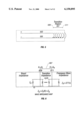
- FIG. 1 shows a side view of a prior art circuit board which can be used in a computer system or other electronic system.
- the circuit board 101 includes two power planes, a voltage plane 103 and a ground plane 105, embedded in the circuit board.
- the voltage plane 103 (such as a VCC plane) may be at a positive or a negative voltage potential (e.g. +5 VDC or -5 VDC).
- the voltage plane typically provides a voltage potential to electronic components of the electronic system incorporating the circuit board.
- Between the power planes is a layer of dielectric material such as prepreg.
- the outer surface of the circuit board 101 is shown in dashed lines.
- circuit boards such as 1) components located on the planar sides 109 or 111 e.g. ICs, other surface mounted electronic components, and electrical traces; 2) embedded structures e.g. plated vias, embedded conductive signal layers, and other embedded power planes; and 3) attachment or mounting mechanisms e.g. screw holes and shielding connectors.
- components located on the planar sides 109 or 111 e.g. ICs, other surface mounted electronic components, and electrical traces
- embedded structures e.g. plated vias, embedded conductive signal layers, and other embedded power planes
- attachment or mounting mechanisms e.g. screw holes and shielding connectors.
- TEM waves are generated from the edge of the circuit board 101 by RF currents in the parallel plane structure of the voltage 103 and ground 105 planes.
- the resultant EM wave profile 107 of the edge generated waves follows the model of co-linear, parallel plate, transmission line.
- the free air capacitance to ground completes the circuit (the receiver) in a similar manner to that of an intentional radio transmitter.
- FIG. 2 is a wave impedance map of the side of a prior art circuit board.
- An RF "induction region” or “impedance transition region” occurs at the abrupt impedance mismatch between the board impedance Z o (the impedance between the power planes) and the free space wave impedance Z a (approximately 377 ⁇ ) of the surrounding air.
- Typical board impedance values may range from less than 10 miliohms to more than 75 ohms.
- RF electrical currents in the power planes generate edge EM emissions to the surrounding air at the abrupt impedance mismatch.
- this approach to building a circuit board maximizes the power planes' transmitting efficiency of delivering TEM RF waves to surrounding free space, which is not desirable.
- the power plane structure will have several natural resonances based upon its physical dimensions.
- a standing wave resonance occurs when the EMI source has a wavelength ⁇ equal to one of the significant dimensions of the circuit board such as, for example, width or length for a rectangular board.
- a high "Q" or resonance potential is achieved when the source frequency or a harmonic of the source frequency is very close to one of the circuit board's natural resonance frequencies such that:
- c speed of light
- f frequency of main resonance
- ⁇ wavelength of the electromagnetic TEM wave.
- the speed of light may be 3 ⁇ 10 8 m/s or less depending on the type of media.
- Some circuit boards (such as a motherboard in a desktop computer system) have a resonant frequency of approximately 200 MHz.
- the resonant frequency is as high as 600 MHz or more. If a clock harmonic is also present at or near these resonant frequencies, the system can easily fail FCC limits.
- the tuned center frequency for each power plane circuit is a function of a number of parameters such as the size and shape of the circuit board power planes, the value and effective complex impedance of the power planes, the dielectric constant of the intermediate dielectric layer, and the separation between the voltage and ground planes.
- the circuit board For a circuit board having two solid, parallel plate power planes, the circuit board has one Q frequency.
- a circuit board with rectangular (length not equal to width) power planes has two Q frequencies, with the particular Q frequency depending upon which edge of the power plane the TEM wave emanates.
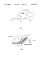
- FIG. 3 shows a perspective view of a prior art circuit board. In addition to showing the edge wave profile, FIG. 3 also shows the propagating direction of the generated EM waves.
- EM radiation generated from ICs e.g. a system processor
- signal traces propagate as RF differential currents and voltages between the voltage plane 303 and ground plane 305 to the edge of the circuit board.
- the largest voltage or current component of the generated waves occurs at the Q frequency of the power planes.
- these voltage waves reach the abrupt impedance mis-match at the edge of the circuit board, they generate EM waves as per the co-linear, parallel plate, transmission line model.
- I RF RF current
- E strength of the voltage field
- a prior art technique for reducing TEM waves generated from the edge of the circuit board is to offset the ground plane 405 from the voltage plane 407.
- An example of this technique is shown in U.S. Pat. No. 5,500,789, entitled “Printed Circuit Board EMI Shielding Apparatus And Associated Methods” which is hereby incorporated by reference in its entirety.
- TEM waves generated or launched from the edge of the voltage plane 407 are "captured” by the further extending ground plane 405 and returned to the system ground.
- a significant amount of EMI radiation is still generated from the edge of the circuit board.
- FIG. 5 shows a side view of a circuit board according to the present invention.
- Voltage plane 503 includes a transition region 507 located at the edge of the voltage plane.
- Transition region 507 has a geometric pattern that produces a deliberate increase in the impedance between the voltage plane 503 and the ground plane 505 in the transition region 507 from the interior side 509 of the transition region to the edge side 511 of the transition region.
- the transition region provides a deliberate increase in the board impedance from an impedance value at the interior of the board to an impedance value that "matches" the impedance of the surrounding air at the edge of the board so as to reduce the EM waves generated from the edge of the circuit board.
- the transition region provides a deliberate increase in board impedance based on the geometric pattern which is applied to the edge of the voltage plane.
- a result of this deliberate increase in impedance is a reduction in RF current between the beginning of the transition region and the edge of the circuit board.
- the "Q" of the entire circuit board is decreased in amplitude because there is no longer an abrupt impedance differential between the circuit board edge and free space.
- FIG. 6 is a wave impedance map of a side of a circuit board according to the present invention.
- Z o is the board power plane impedance, or the impedance between the voltage and ground planes, at an interior region of the power planes.
- the transition region broad impedance Z t (X) deliberately increases from approximately the value of Z o at the interior side 609 (where Z t (X interior ) approximately equals Z o ) towards the impedance of the surrounding air Z a at the edge side 611 of the transition region 611.
- the impedance value Z t (X edge ) at the edge side of the transition region may range from being slightly less (2 or 3 ohms) than Z a to somewhat less (10 ohms) depending upon the practical constraints and desired reduction in EM field intensity.
- Z t (X edge ) is to be no less than 377 Ohm.
- RF currents generated by ICs and traces located at an interior of the circuit board propagate along the voltage plane 503 towards the transition region 507.
- the geometric pattern provides a deliberate increase in the impedance between the power planes 503 and 505, which corresponds to providing an RF voltage drop to forming TEM waves.
- certain frequencies of RF current from the voltage power plane select the path into the ground plane 505 prior to reaching the edge side 511 of the transition region.
- the overall effect of this transition region is to provide a low pass filter function utilizing inter-planar inductance and bi-planar capacitance which significantly attenuates high frequency emissions. See FIG. 7A.
- the successive reduction in RF current in the transition region significantly reduces the power associated with the RF current at the edge side 511 of the transition region 507 such that the EM waves generate from the RF current reaching the edge are significantly reduced as well.
- the "poles" of the low pass frequency function can be adjusted by manipulating the inductance values of the transition region.
- the inductance values of the resultant low pass filter can be adjusted by varying the width between the stripes 751 of the power plane.
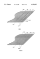
- FIG. 7B shows a perspective view of a circuit board according to the present invention.
- Transition region 707 of voltage plane 703 has a geometric configuration that provides a deliberate increase in the impedance between the voltage and ground planes 703 and 705 from the interior side of the transition region to the edge side of the transition region. It is understood that the individual segments of the transition region of the voltage plane 707 would be electrically coupled together.
- the width of the transition region is approximately 1/4 inch.
- a transition region width for other circuit boards may range from 0.1" ⁇ W ⁇ 3.0".
- Still other circuit boards may have transition regions of greater or lesser widths.
- One factor for determining the appropriate width of the transition region is the main circuit board resonance frequency of the voltage power plane structure. The lower the main circuit board resonance frequency, the greater the required width to significantly reduce the generated waves. For all frequencies of interest, a minimum desired width of a transition region is:
- h is the separation of the voltage plane and the ground plane.
- the width of a transition region is: ##EQU1## where ⁇ is the frequency of interest.
- the minimum desired transition region width is:
- the wavelengths are too large to practically provide an effective transition region to reduce EM waves at those frequencies.
- such low frequencies are typically well below the Q frequency of the voltage/ground plane structure such that the component of the EM waves generated at such frequencies is insignificant.
- the lower the frequency the lower the required tolerance is for the connector openings of the EMI shield.
- the width of the transition region is preferably just wide enough to be effective in reducing edge generated waves at the Q frequency or at other frequencies that make up a significant component of the EMI profile (e.g., the system processor clock frequencies).
- one advantage of the present invention is that it is effective in reducing edge waves at high frequencies which require a containment shield to be very robust, have minimal seams, and have maximized edge-to-edge contact.
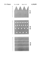
- FIGS. 8A, 8B, and 8C show top views of three exemplary geometric configurations of voltage plane transition regions for providing a deliberate increase in the impedance between a voltage and ground plane.
- the right sides of FIGS. 8A, 8B, and 8C are located towards the edge side of the transition region and the left sides are located towards an interior side of the transition region.
- geometric configurations of a transition region of a voltage plane that provide a deliberate increase in board impedance from the interior side to the edge side typically have a decrease in density of plane material (or an increase in void space) from the interior side to the edge side.
- the 8B includes a plurality of holes that increase in density from the interior side to the edge side of the transition region.
- the bases of the triangles are located towards the interior side of the board and the pointed ends are oriented towards the edge side of the board. This decrease in the density of plane material provides a deliberate increase in the board impedance in the transition region going from the interior side of the transition region towards the edge side of the transition region.
- FIGS. 9 through 14 are perspective views showing the positional orientation between power planes embedded in a circuit board. These Figures illustrate exemplary transition region geometric configurations for providing a deliberate increase in the impedance from an interior side of a transition region to an edge side of the transition region.
- the width of the transition regions in FIGS. 9-14 have been disproportionately exaggerated with respect to the width and length of the power planes so as to more clearly illustrate the geometric configuration of the transition region.
- Also not shown in FIGS. 9-14 are holes and other spaces in the power plane that allow for plated vias and other circuit board structures to pass though the circuit board. These conventional holes or spaces are not shown in the Figures of this application in order to more clearly illustrate the inventive aspects of the circuit boards according to the present invention. However it is understood that the circuit boards according to the present invention may include these conventional holes or spaces.
- FIG. 9 shows an example of a transition region having a striped geometric configuration.
- the stripes 917 of transition region 907 of the voltage plane 903 run parallel with edge 911 of transition region 907.
- the width of the stripes 917 decreases from the interior side 909 of the transition region to the edge side 911 of the transition region to provide a deliberate increase in impedance from the interior side 909 to the edge side 911.
- the shunt capacitance of each stripe combined with the series inductance of a small trace 919 (preferably copper with some boards) connecting each stripe in effect forms a multi-pole high frequency filter. See FIG. 7A.
- the change in width of the stripes from the board side to the edge side of the transition region may be varied to vary the desired rate of the deliberate increase in impedance.
- the spacings between the stripes may also be varied within a transition region to provide a deliberate increase in impedance.
- FIG. 10 shows an example of a transition region having a hole or void geometric configuration.
- transition region 1007 includes rows of holes 1008 which are voids in the voltage plane 1003 material.
- the number of holes in a row, the length of a row, and the density of the rows all increase from the interior side 1009 of the transition region 1007 to the edge side 1011 of the transition region to provide a deliberate increase in the board impedance.
- FIG. 11 shows an example of a dot transition region.
- the transition region of the voltage plane 1103 is made up of connected dots 1115 that decrease in density from the interior side 1109 to the edge side 1111 of the transition region to provide a deliberate increase in the board impedance.
- FIG. 12 shows an example of a transition region having a triangle (or stealth) geometric configuration.
- Transition region 1207 includes a plurality of triangles having the bases positioned towards the interior of the voltage plane 1203 and the pointed ends positioned toward the edge of the voltage plane.
- the resultant edge of the voltage plane has a saw-tooth form.
- the triangle shapes shown in FIG. 12 have straight slope edges. However, the slope edges may have other forms such as a logarithmic slope (see FIG. 14), a "stair-shaped" slope, or a stair-shaped logarithmic slope.
- FIG. 13 shows an example of a transition region having a grid geometric configuration.
- the grid configuration of FIG. 13 include a plurality of grid lines 1319 running parallel with the edge side 1311 of transition region 1307 and a plurality of grid lines 1321 ruling perpendicular to the edge side 1311.
- the parallel running grid lines 1319 decrease in density from the interior side 1309 to the edge side 1311 to provide a decrease in the density of the voltage plane 1303 from the interior side 1309 to the edge side 1311.
- other grid configurations may be used to provide a deliberate increase in the impedance from the interior side to the edge side.
- diagonal lines may be used.
- the grid lines 1321 running perpendicular to the edge side 1311 may extend from the interior of the voltage plane 1303 at varying lengths.
- the widths of the transition region grid lines may decrease from the interior side to the edge side of a transition region.
- FIG. 14 shows an example of a transition region having a logarithmic sloped triangle geometric configuration.
- the slopes 1415 of the triangles have a slope that follows a logarithmic function.
- An advantage of having a logarithmic slope is that the configuration provides the transition region with a deliberate increase in impedance that is exponential and thus more closely matches to the decline in RF current from the interior side 1409 to the edge side 1411 of the transition region.
- the power of the RF waves is:
- the impedance increases at a faster rate at the interior side 1409 of the transition region 1407 than at the edge side 1411. Having a faster deliberate increase at the interior side and a slower deliberate increase at the edge side is advantageous in that the change in impedance at the interior side is more dramatic where the intensity of the RF current is greater. As the RF current reaches the edge side 1411, the slower change in the deliberate increase has a less adverse affect in that the strength of the RF current has significantly decreased at that point.
- FIG. 18 is a graph showing a decrease in RF current across a transition region having a linear deliberate increase in impedance. From the board side to the edge side of the transition region, the RF current tapers off in a non linear manner. For a transition region of width w, a board impedance of Z b , with Z a being the impedance of air, the linear change in impedance is: ##EQU3##
- FIG. 19 is a graph showing a decrease in RF current across a transition region having a non linear deliberate increase in impedance.
- the RF current tapers off in a faster, more linear fashion, which reduces reflections of RF waves inside the power planes of the circuit board.
- FIGS. 8-14 are exemplary of geometric configurations that provide a deliberate increase in the board impedance in the transition region from the interior side to the edge side. Based upon the teachings presented herein, those skilled in the art will appreciate that other geometric configurations may be used to provide a transition region with a deliberate increase in board impedance.
- FIGS. 8-14 show only one perimeter side of a voltage plane having a transition region
- other circuit boards according to the present invention may include a transition region for each perimeter edge of the circuit board.
- a foot print of the voltage plane having a transition region geometric configuration(s) is designed with the use of a Computer Assisted Design (CAD) program.
- CAD Computer Assisted Design
- the resultant foot print is then photo etched during a photolithography process onto a solid conductive layer (such as a 1 ounce copper layer having a thickness of 1.4 mills) covering a layer of dielectric material such as a 5 mil layer of prepreg or FR-4 fiber glass resin laminate. Additional layers of dielectric and conductive layers are then added to the initial voltage/ground structure.
- circuit boards incorporating multiple voltage and ground layers such as a circuit board incorporating capacitive planes
- conductive and dielectric layer groups are conventionally formed separately and then sandwiched together to form a multi-layer circuit board. See the patent entitled “Printed Circuit Board (PCB) Including Channeled Capacitive Plane Structure", U.S. Pat. No. 5,912,809 , filed on Jan. 21, 1997 and having a common assignee, which is hereby incorporated by reference in its entirety.
- each co-extensive voltage plane may have a transition region for each side located at the perimeter of the circuit board.
- a single ground plane may be closely positioned between two voltage planes both having transition regions on the voltage plane edges at the perimeter of the circuit board.
- circuit boards incorporate multiple voltage planes in the same circuit board layer.
- PCB printed Circuit Board
- Another example is a circuit board having a layer of multiple conductive patches at the same potential and electrically coupled together.
- those voltage planes of the layer having edges at the perimeter of the circuit board would include a transition region having a deliberate increase in impedance for each perimeter side.
- all edges of a voltage plane, including those edges located in the interior of the circuit board adjacent to other voltage planes of the same layer would also have a transition region.
- the exemplary transition region configurations shown in FIGS. 8-14 have been shown incorporated with solid power planes. It is understood that a solid power plane may include via holes, drill holes, or other voids in the plane. However, the present invention may also be incorporated with other types of power planes such as cross hatch and slotted power planes. With these circuit boards, the density of the "non-solid" power plane material decreases from the interior side to the edge side of the transition region so as to provide a deliberate increase in the board impedance in accordance with the present invention. In one example of an embedded grid power plane, the spacings between the grid lines increase from the interior side to the edge side of the transition region.
- a deliberate increase in impedance from an interior side to an edge side of a transition region of a circuit board may also be achieved by providing the portion of the ground plane extending into the transition region with a geometric configuration such as those shown in FIGS. 8-14.
- FIG. 15 represents an alternative embodiment for providing a circuit board with a transition region having a deliberate increase in impedance from the interior side to the edge side of the transition region according to the present invention.
- the deliberate increase in board impedance is achieved by providing an increase in the distance between the voltage 1503 and ground 1505 planes from the interior side 1509 to the edge side 1511 of the transition region 1507.
- FIG. 16 is a side view of an exemplary circuit board according to the present invention having a deliberate increase in impedance from the interior side to the edge side of the transition region by proving an increase in the distance between the voltage plane and ground plane from the interior side to the edge side.
- the transition region portion 1607 of the voltage plane 1603 has a stair-step profile.
- Each horizontal (relative to the view shown in FIG. 16) layer of the transition portion of the voltage plane such as layer 1621 is formed by the successive etching of conductive layers during the formation of embedded trace layers located in an internal region of the circuit board.
- Each horizontal layer of the stair step is formed successively further away from ground plane 1605.
- Inter-planar vertical connections of the horizontal layers of the transition portion of the voltage plane are obtained by plated through holes, plated slots, or filled holes or slots interconnecting the horizontal layers.
- One advantage of the transition board of FIG. 16 is that the form of the effective slope of the transition region portion of the voltage plane can be more accurately controlled.
- An increase between the voltage and ground planes can also be achieved by sloping the ground plane away from the voltage plane or by sloping both planes away from each other.
- a deliberate increase in the board impedance in the transition region from the interior side to the edge side is obtained by providing the portion of the dielectric layer located between the voltage and ground plane with a material having an increasing dielectric constant from the interior side of the transition region to the edge side of the transition region.
- the increase of the dielectric constant of the transition region portion of the dielectric layer provides a deliberate increase in the impedance between the voltage and ground planes.
- Circuit boards including transition regions having a deliberate increase in board impedances according to the present invention may be utilized in a number of different types of computer systems and other types of electronic systems to reduce the EMI emissions of those systems.
- such circuit boards may be used in desktop computers such as the OPTIPLEX sold by DELL COMPUTER CORP.
- portable computers also referred to as notebook or laptop computers
- portable computers such as the LATITUDE CP family of portable computers and the INSPIRON 3000, 3200
- 7000 portable computers sold by the DELL COMPUTER CORP.
- servers such as the POWER EDGE 6300 sold by DELL COMPUTER CORP.
- These computer system types typically include a system processor and associated system memory (e.g. RAM) along with peripheral devices operably coupled to the system processor.
- the system processor typically is physically coupled to a circuit board such as a motherboard or a daughter card of the computer system.
- a circuit board such as a motherboard or a daughter card of the computer system.
- the motherboard, daughter card, and/or any other circuit boards incorporating power planes may include at their perimeters transition regions having a deliberate increase in impedance according to the present invention.
- FIG. 17 shows a perspective, cutaway view of a portable computer system incorporating a circuit board having a transition region according to the present invention.
- Portable computer system 1701 includes a system processor 1703 and system memory DRAM chips 1705 mounting to circuit board 1709.
- the edges of the circuit board include transition regions having deliberate increases in board impedances from a board impedance value at the interior of the circuit board towards a board impedance value of surrounding air.
- items typically found in a portable computer system such as a keyboard, power supply, I/O controllers, and other integrated circuits, some of which are mounted to circuit board 1709.
Abstract
Description
SE.sup.(dB) =A.sup.(dB)+ R.sup.(dB).
SE.sup.(dB) =20 log F1/F2.sup.(dB).
λ=c/f
W.sub.(mm) =20*h.sub.(mm)
W.sub.min =20.sup.(0.125) (mm)
W.sub.min =2.5.sub.(mm)
W.sub.min =75.sub.(mm) or 7.5.sub.(cm)
P.sub.waves =I.sup.2.sub.RFcurrent * Z.sub.board impedance.
Claims (43)
Priority Applications (1)
| Application Number | Priority Date | Filing Date | Title |
|---|---|---|---|
| US09/236,706 US6150895A (en) | 1999-01-25 | 1999-01-25 | Circuit board voltage plane impedance matching |
Applications Claiming Priority (1)
| Application Number | Priority Date | Filing Date | Title |
|---|---|---|---|
| US09/236,706 US6150895A (en) | 1999-01-25 | 1999-01-25 | Circuit board voltage plane impedance matching |
Publications (1)
| Publication Number | Publication Date |
|---|---|
| US6150895A true US6150895A (en) | 2000-11-21 |
Family
ID=22890608
Family Applications (1)
| Application Number | Title | Priority Date | Filing Date |
|---|---|---|---|
| US09/236,706 Expired - Lifetime US6150895A (en) | 1999-01-25 | 1999-01-25 | Circuit board voltage plane impedance matching |
Country Status (1)
| Country | Link |
|---|---|
| US (1) | US6150895A (en) |
Cited By (31)
| Publication number | Priority date | Publication date | Assignee | Title |
|---|---|---|---|---|
| US6347041B1 (en) * | 2000-01-21 | 2002-02-12 | Dell Usa, L.P. | Incremental phase correcting mechanisms for differential signals to decrease electromagnetic emissions |
| US20030038639A1 (en) * | 1999-12-23 | 2003-02-27 | Dell Products L.P. | Data processing systems having mismatched impedance components |
| US20030057966A1 (en) * | 2001-07-13 | 2003-03-27 | Kenji Shimazaki | Electromagnetic interference analysis method and apparatus |
| US6587908B2 (en) * | 1999-02-12 | 2003-07-01 | Hewlett-Packard Development Company, L.P. | Processor design with improved condition sensing |
| US20040050585A1 (en) * | 2002-09-17 | 2004-03-18 | International Business Machines Corporation | Method to obtain high density signal wires with low resistance in an electronic package |
| US6734755B2 (en) | 2002-05-16 | 2004-05-11 | Corning Incorporated | Broadband uniplanar coplanar transition |
| US6775122B1 (en) * | 1999-12-28 | 2004-08-10 | Intel Corporation | Circuit board with added impedance |
| US20040197284A1 (en) * | 2003-04-04 | 2004-10-07 | Frederic Auguste | Cosmetic composition comprising a volatile fatty phase |
| US20040201971A1 (en) * | 2003-04-08 | 2004-10-14 | Fessler John Thomas | Printed circuit board having outer power planes |
| US6900992B2 (en) * | 2001-09-18 | 2005-05-31 | Intel Corporation | Printed circuit board routing and power delivery for high frequency integrated circuits |
| US20060035607A1 (en) * | 2004-08-10 | 2006-02-16 | Sony Ericsson Mobile Communications Ab | Reduction of Near Field Electro-Magnetic Scattering Using High Impedance Metallization Terminations |
| US20060274472A1 (en) * | 2003-12-15 | 2006-12-07 | Kenichi Saito | Noise filter mounting structure |
| US7361843B2 (en) | 2005-09-28 | 2008-04-22 | Dell Products L.P. | AC coupling of power plane sections using improved capacitance stitching material |
| US20080143621A1 (en) * | 2006-11-30 | 2008-06-19 | Diaz Rodolfo E | Electromagnetic reactive edge treatment |
| US7465882B2 (en) | 2006-12-13 | 2008-12-16 | International Business Machines Corporation | Ceramic substrate grid structure for the creation of virtual coax arrangement |
| US20090290315A1 (en) * | 2006-07-20 | 2009-11-26 | Panasonic Corporation | Communication device and electronic apparatus using the same |
| US7675729B2 (en) | 2003-12-22 | 2010-03-09 | X2Y Attenuators, Llc | Internally shielded energy conditioner |
| US7688565B2 (en) | 1997-04-08 | 2010-03-30 | X2Y Attenuators, Llc | Arrangements for energy conditioning |
| US7733621B2 (en) | 1997-04-08 | 2010-06-08 | X2Y Attenuators, Llc | Energy conditioning circuit arrangement for integrated circuit |
| US7768763B2 (en) | 1997-04-08 | 2010-08-03 | X2Y Attenuators, Llc | Arrangement for energy conditioning |
| US7782587B2 (en) | 2005-03-01 | 2010-08-24 | X2Y Attenuators, Llc | Internally overlapped conditioners |
| US7817397B2 (en) | 2005-03-01 | 2010-10-19 | X2Y Attenuators, Llc | Energy conditioner with tied through electrodes |
| US8026777B2 (en) | 2006-03-07 | 2011-09-27 | X2Y Attenuators, Llc | Energy conditioner structures |
| US20120300872A1 (en) * | 2011-05-27 | 2012-11-29 | Samsung Electronics Co., Ltd. | In-band data communication system using wireless power |
| US20130192865A1 (en) * | 2010-03-15 | 2013-08-01 | Nec Corporation | Noise suppression structure |
| US20140118962A1 (en) * | 2012-10-29 | 2014-05-01 | Cisco Technology, Inc. | Current Redistribution in a Printed Circuit Board |
| US8927879B2 (en) | 2010-11-22 | 2015-01-06 | International Business Machines Corporation | Crosstalk reduction between signal layers in a multilayered package by variable-width mesh plane structures |
| US9054094B2 (en) | 1997-04-08 | 2015-06-09 | X2Y Attenuators, Llc | Energy conditioning circuit arrangement for integrated circuit |
| US9420734B2 (en) | 2014-04-01 | 2016-08-16 | Advanced Micro Devices, Inc. | Combined electromagnetic shield and thermal management device |
| US20170085243A1 (en) * | 2015-09-21 | 2017-03-23 | Intel Corporation | Impedance matching interconnect |
| US11277903B2 (en) * | 2019-03-28 | 2022-03-15 | Intel Corporation | Pattern-edged metal-plane resonance-suppression |
Citations (33)
| Publication number | Priority date | Publication date | Assignee | Title |
|---|---|---|---|---|
| US4760400A (en) * | 1986-07-15 | 1988-07-26 | Canadian Marconi Company | Sandwich-wire antenna |
| US4927742A (en) * | 1987-01-14 | 1990-05-22 | Kollmorgen Corporation | Multilayer printed wiring boards |
| US5010641A (en) * | 1989-06-30 | 1991-04-30 | Unisys Corp. | Method of making multilayer printed circuit board |
| US5025116A (en) * | 1989-01-27 | 1991-06-18 | Nippon Cmk Corp. | Printed wiring board having electromagnetic wave shielding layer |
| US5030800A (en) * | 1989-01-27 | 1991-07-09 | Nippon Cmk Corp. | Printed wiring board with an electronic wave shielding layer |
| US5079069A (en) * | 1989-08-23 | 1992-01-07 | Zycon Corporation | Capacitor laminate for use in capacitive printed circuit boards and methods of manufacture |
| US5112648A (en) * | 1990-07-18 | 1992-05-12 | Nippon Cmk Corp. | Method of manufacturing a printed circuit board |
| US5140110A (en) * | 1986-03-13 | 1992-08-18 | Nintendo Co. Ltd. | Printed circuit board capable of preventing electromagnetic interference |
| US5155655A (en) * | 1989-08-23 | 1992-10-13 | Zycon Corporation | Capacitor laminate for use in capacitive printed circuit boards and methods of manufacture |
| US5161086A (en) * | 1989-08-23 | 1992-11-03 | Zycon Corporation | Capacitor laminate for use in capacitive printed circuit boards and methods of manufacture |
| US5173150A (en) * | 1990-04-23 | 1992-12-22 | Mitsubishi Gas Chemical Co., Ltd. | Process for producing printed circuit board |
| US5196230A (en) * | 1990-04-18 | 1993-03-23 | Nippon Cmk Corp. | Method for connecting an electromagnetic wave shielding layer with a ground circuit in a printed circuit board |
| US5236736A (en) * | 1990-10-15 | 1993-08-17 | Nippon Cmk Corp. | Method for manufacturing an electromagnetic wave shield printed wiring board |
| US5262596A (en) * | 1990-10-15 | 1993-11-16 | Nippon Cmk Corp. | Printed wiring board shielded from electromagnetic wave |
| US5261153A (en) * | 1992-04-06 | 1993-11-16 | Zycon Corporation | In situ method for forming a capacitive PCB |
| US5293004A (en) * | 1991-09-02 | 1994-03-08 | Nippon Cmk Corp. | Printed circuit board having an electromagnetic shielding layer |
| US5291653A (en) * | 1991-09-30 | 1994-03-08 | Nippon Cmk Corp. | Manufacturing printed wiring boards having electromagnetic wave shielding |
| US5315069A (en) * | 1992-10-02 | 1994-05-24 | Compaq Computer Corp. | Electromagnetic radiation reduction technique using grounded conductive traces circumscribing internal planes of printed circuit boards |
| US5324766A (en) * | 1989-07-07 | 1994-06-28 | Mitsui Petrochemical Industries, Ltd. | Resin composition for forming plated layer and use thereof |
| US5416667A (en) * | 1992-07-03 | 1995-05-16 | Nippon Cmk Corp. | Printed wiring board having an electromagnetic wave shielding layer |
| US5418690A (en) * | 1993-06-11 | 1995-05-23 | International Business Machines Corporation | Multiple wiring and X section printed circuit board technique |
| US5428506A (en) * | 1990-08-02 | 1995-06-27 | International Business Machines Corp. | Circuit board EMI suppressor including a lossy dielectric layer |
| US5494781A (en) * | 1993-08-26 | 1996-02-27 | Matsushita Electric Works, Ltd. | Method for manufacturing printed circuit board |
| US5500789A (en) * | 1994-12-12 | 1996-03-19 | Dell Usa, L.P. | Printed circuit board EMI shielding apparatus and associated methods |
| US5633479A (en) * | 1994-07-26 | 1997-05-27 | Kabushiki Kaisha Toshiba | Multilayer wiring structure for attaining high-speed signal propagation |
| US5635767A (en) * | 1995-06-02 | 1997-06-03 | Motorola, Inc. | Semiconductor device having built-in high frequency bypass capacitor |
| US5639989A (en) * | 1994-04-19 | 1997-06-17 | Motorola Inc. | Shielded electronic component assembly and method for making the same |
| US5682124A (en) * | 1993-02-02 | 1997-10-28 | Ast Research, Inc. | Technique for increasing the range of impedances for circuit board transmission lines |
| US5841074A (en) * | 1996-03-12 | 1998-11-24 | International Business Machines Corporation | Backplane power distribution system having impedance variations in the form of spaced voids |
| US5912597A (en) * | 1994-03-31 | 1999-06-15 | Canon Kabushiki Kaisha | Printed circuit board |
| US5912809A (en) * | 1997-01-21 | 1999-06-15 | Dell Usa, L.P. | Printed circuit board (PCB) including channeled capacitive plane structure |
| US5926377A (en) * | 1997-03-31 | 1999-07-20 | Fujitsu Limited | Multilayer printed board |
| US5966294A (en) * | 1996-12-20 | 1999-10-12 | Nec Corporation | Printed circuit board for prevention of unintentional electromagnetic interference |
-
1999
- 1999-01-25 US US09/236,706 patent/US6150895A/en not_active Expired - Lifetime
Patent Citations (33)
| Publication number | Priority date | Publication date | Assignee | Title |
|---|---|---|---|---|
| US5140110A (en) * | 1986-03-13 | 1992-08-18 | Nintendo Co. Ltd. | Printed circuit board capable of preventing electromagnetic interference |
| US4760400A (en) * | 1986-07-15 | 1988-07-26 | Canadian Marconi Company | Sandwich-wire antenna |
| US4927742A (en) * | 1987-01-14 | 1990-05-22 | Kollmorgen Corporation | Multilayer printed wiring boards |
| US5025116A (en) * | 1989-01-27 | 1991-06-18 | Nippon Cmk Corp. | Printed wiring board having electromagnetic wave shielding layer |
| US5030800A (en) * | 1989-01-27 | 1991-07-09 | Nippon Cmk Corp. | Printed wiring board with an electronic wave shielding layer |
| US5010641A (en) * | 1989-06-30 | 1991-04-30 | Unisys Corp. | Method of making multilayer printed circuit board |
| US5324766A (en) * | 1989-07-07 | 1994-06-28 | Mitsui Petrochemical Industries, Ltd. | Resin composition for forming plated layer and use thereof |
| US5155655A (en) * | 1989-08-23 | 1992-10-13 | Zycon Corporation | Capacitor laminate for use in capacitive printed circuit boards and methods of manufacture |
| US5161086A (en) * | 1989-08-23 | 1992-11-03 | Zycon Corporation | Capacitor laminate for use in capacitive printed circuit boards and methods of manufacture |
| US5079069A (en) * | 1989-08-23 | 1992-01-07 | Zycon Corporation | Capacitor laminate for use in capacitive printed circuit boards and methods of manufacture |
| US5196230A (en) * | 1990-04-18 | 1993-03-23 | Nippon Cmk Corp. | Method for connecting an electromagnetic wave shielding layer with a ground circuit in a printed circuit board |
| US5173150A (en) * | 1990-04-23 | 1992-12-22 | Mitsubishi Gas Chemical Co., Ltd. | Process for producing printed circuit board |
| US5112648A (en) * | 1990-07-18 | 1992-05-12 | Nippon Cmk Corp. | Method of manufacturing a printed circuit board |
| US5428506A (en) * | 1990-08-02 | 1995-06-27 | International Business Machines Corp. | Circuit board EMI suppressor including a lossy dielectric layer |
| US5236736A (en) * | 1990-10-15 | 1993-08-17 | Nippon Cmk Corp. | Method for manufacturing an electromagnetic wave shield printed wiring board |
| US5262596A (en) * | 1990-10-15 | 1993-11-16 | Nippon Cmk Corp. | Printed wiring board shielded from electromagnetic wave |
| US5293004A (en) * | 1991-09-02 | 1994-03-08 | Nippon Cmk Corp. | Printed circuit board having an electromagnetic shielding layer |
| US5291653A (en) * | 1991-09-30 | 1994-03-08 | Nippon Cmk Corp. | Manufacturing printed wiring boards having electromagnetic wave shielding |
| US5261153A (en) * | 1992-04-06 | 1993-11-16 | Zycon Corporation | In situ method for forming a capacitive PCB |
| US5416667A (en) * | 1992-07-03 | 1995-05-16 | Nippon Cmk Corp. | Printed wiring board having an electromagnetic wave shielding layer |
| US5315069A (en) * | 1992-10-02 | 1994-05-24 | Compaq Computer Corp. | Electromagnetic radiation reduction technique using grounded conductive traces circumscribing internal planes of printed circuit boards |
| US5682124A (en) * | 1993-02-02 | 1997-10-28 | Ast Research, Inc. | Technique for increasing the range of impedances for circuit board transmission lines |
| US5418690A (en) * | 1993-06-11 | 1995-05-23 | International Business Machines Corporation | Multiple wiring and X section printed circuit board technique |
| US5494781A (en) * | 1993-08-26 | 1996-02-27 | Matsushita Electric Works, Ltd. | Method for manufacturing printed circuit board |
| US5912597A (en) * | 1994-03-31 | 1999-06-15 | Canon Kabushiki Kaisha | Printed circuit board |
| US5639989A (en) * | 1994-04-19 | 1997-06-17 | Motorola Inc. | Shielded electronic component assembly and method for making the same |
| US5633479A (en) * | 1994-07-26 | 1997-05-27 | Kabushiki Kaisha Toshiba | Multilayer wiring structure for attaining high-speed signal propagation |
| US5500789A (en) * | 1994-12-12 | 1996-03-19 | Dell Usa, L.P. | Printed circuit board EMI shielding apparatus and associated methods |
| US5635767A (en) * | 1995-06-02 | 1997-06-03 | Motorola, Inc. | Semiconductor device having built-in high frequency bypass capacitor |
| US5841074A (en) * | 1996-03-12 | 1998-11-24 | International Business Machines Corporation | Backplane power distribution system having impedance variations in the form of spaced voids |
| US5966294A (en) * | 1996-12-20 | 1999-10-12 | Nec Corporation | Printed circuit board for prevention of unintentional electromagnetic interference |
| US5912809A (en) * | 1997-01-21 | 1999-06-15 | Dell Usa, L.P. | Printed circuit board (PCB) including channeled capacitive plane structure |
| US5926377A (en) * | 1997-03-31 | 1999-07-20 | Fujitsu Limited | Multilayer printed board |
Non-Patent Citations (2)
| Title |
|---|
| Howard W. Johnson and Martin Graham, "High-Speed Digital Design: A Handbook of Black Magic", 1993, pp. 189-221. |
| Howard W. Johnson and Martin Graham, High Speed Digital Design: A Handbook of Black Magic , 1993, pp. 189 221. * |
Cited By (69)
| Publication number | Priority date | Publication date | Assignee | Title |
|---|---|---|---|---|
| US7733621B2 (en) | 1997-04-08 | 2010-06-08 | X2Y Attenuators, Llc | Energy conditioning circuit arrangement for integrated circuit |
| US8018706B2 (en) | 1997-04-08 | 2011-09-13 | X2Y Attenuators, Llc | Arrangement for energy conditioning |
| US9054094B2 (en) | 1997-04-08 | 2015-06-09 | X2Y Attenuators, Llc | Energy conditioning circuit arrangement for integrated circuit |
| US9036319B2 (en) | 1997-04-08 | 2015-05-19 | X2Y Attenuators, Llc | Arrangement for energy conditioning |
| US9019679B2 (en) | 1997-04-08 | 2015-04-28 | X2Y Attenuators, Llc | Arrangement for energy conditioning |
| US8004812B2 (en) | 1997-04-08 | 2011-08-23 | X2Y Attenuators, Llc | Energy conditioning circuit arrangement for integrated circuit |
| US7920367B2 (en) | 1997-04-08 | 2011-04-05 | X2Y Attenuators, Llc | Method for making arrangement for energy conditioning |
| US8587915B2 (en) | 1997-04-08 | 2013-11-19 | X2Y Attenuators, Llc | Arrangement for energy conditioning |
| US8023241B2 (en) | 1997-04-08 | 2011-09-20 | X2Y Attenuators, Llc | Arrangement for energy conditioning |
| US7688565B2 (en) | 1997-04-08 | 2010-03-30 | X2Y Attenuators, Llc | Arrangements for energy conditioning |
| US7916444B2 (en) | 1997-04-08 | 2011-03-29 | X2Y Attenuators, Llc | Arrangement for energy conditioning |
| US7768763B2 (en) | 1997-04-08 | 2010-08-03 | X2Y Attenuators, Llc | Arrangement for energy conditioning |
| US9373592B2 (en) | 1997-04-08 | 2016-06-21 | X2Y Attenuators, Llc | Arrangement for energy conditioning |
| US6587908B2 (en) * | 1999-02-12 | 2003-07-01 | Hewlett-Packard Development Company, L.P. | Processor design with improved condition sensing |
| US20030038639A1 (en) * | 1999-12-23 | 2003-02-27 | Dell Products L.P. | Data processing systems having mismatched impedance components |
| US6788073B2 (en) * | 1999-12-23 | 2004-09-07 | Dell Products L.P. | Data processing systems having mismatched impedance components |
| US6775122B1 (en) * | 1999-12-28 | 2004-08-10 | Intel Corporation | Circuit board with added impedance |
| US6347041B1 (en) * | 2000-01-21 | 2002-02-12 | Dell Usa, L.P. | Incremental phase correcting mechanisms for differential signals to decrease electromagnetic emissions |
| US20030057966A1 (en) * | 2001-07-13 | 2003-03-27 | Kenji Shimazaki | Electromagnetic interference analysis method and apparatus |
| US6754598B2 (en) * | 2001-07-13 | 2004-06-22 | Matsushita Electric Industrial Co., Ltd. | Electromagnetic interference analysis method and apparatus |
| US6900992B2 (en) * | 2001-09-18 | 2005-05-31 | Intel Corporation | Printed circuit board routing and power delivery for high frequency integrated circuits |
| US6734755B2 (en) | 2002-05-16 | 2004-05-11 | Corning Incorporated | Broadband uniplanar coplanar transition |
| US20040050585A1 (en) * | 2002-09-17 | 2004-03-18 | International Business Machines Corporation | Method to obtain high density signal wires with low resistance in an electronic package |
| US6762367B2 (en) | 2002-09-17 | 2004-07-13 | International Business Machines Corporation | Electronic package having high density signal wires with low resistance |
| US20040197284A1 (en) * | 2003-04-04 | 2004-10-07 | Frederic Auguste | Cosmetic composition comprising a volatile fatty phase |
| US20040201971A1 (en) * | 2003-04-08 | 2004-10-14 | Fessler John Thomas | Printed circuit board having outer power planes |
| US7016198B2 (en) | 2003-04-08 | 2006-03-21 | Lexmark International, Inc. | Printed circuit board having outer power planes |
| US7382216B2 (en) * | 2003-12-15 | 2008-06-03 | Murata Manufacturing Co., Ltd | Noise filter mounting structure |
| US20060274472A1 (en) * | 2003-12-15 | 2006-12-07 | Kenichi Saito | Noise filter mounting structure |
| US7675729B2 (en) | 2003-12-22 | 2010-03-09 | X2Y Attenuators, Llc | Internally shielded energy conditioner |
| WO2006022846A1 (en) | 2004-08-10 | 2006-03-02 | Sony Ericsson Mobile Communications Ab | Reduction of near field electro-magnetic scattering using high impedance metallization terminations |
| US20080214136A1 (en) * | 2004-08-10 | 2008-09-04 | Gerard James Hayes | Reduction of near field electro-magnetic scattering using high impedance metallization terminations |
| US20060035607A1 (en) * | 2004-08-10 | 2006-02-16 | Sony Ericsson Mobile Communications Ab | Reduction of Near Field Electro-Magnetic Scattering Using High Impedance Metallization Terminations |
| US8155616B2 (en) * | 2004-08-10 | 2012-04-10 | Sony Mobile Communications Ab | Reduction of near field electro-magnetic scattering using high impedance metallization terminations |
| US7376408B2 (en) * | 2004-08-10 | 2008-05-20 | Sony Ericsson Mobile Communications Ab | Reduction of near field electro-magnetic scattering using high impedance metallization terminations |
| US7974062B2 (en) | 2005-03-01 | 2011-07-05 | X2Y Attenuators, Llc | Internally overlapped conditioners |
| US7782587B2 (en) | 2005-03-01 | 2010-08-24 | X2Y Attenuators, Llc | Internally overlapped conditioners |
| US8547677B2 (en) | 2005-03-01 | 2013-10-01 | X2Y Attenuators, Llc | Method for making internally overlapped conditioners |
| US9001486B2 (en) | 2005-03-01 | 2015-04-07 | X2Y Attenuators, Llc | Internally overlapped conditioners |
| US8014119B2 (en) | 2005-03-01 | 2011-09-06 | X2Y Attenuators, Llc | Energy conditioner with tied through electrodes |
| US7817397B2 (en) | 2005-03-01 | 2010-10-19 | X2Y Attenuators, Llc | Energy conditioner with tied through electrodes |
| US7361843B2 (en) | 2005-09-28 | 2008-04-22 | Dell Products L.P. | AC coupling of power plane sections using improved capacitance stitching material |
| US8026777B2 (en) | 2006-03-07 | 2011-09-27 | X2Y Attenuators, Llc | Energy conditioner structures |
| US20090290315A1 (en) * | 2006-07-20 | 2009-11-26 | Panasonic Corporation | Communication device and electronic apparatus using the same |
| US8014161B2 (en) * | 2006-07-20 | 2011-09-06 | Panasonic Corporation | Communication device and electronic apparatus using the same |
| US20100315302A1 (en) * | 2006-11-30 | 2010-12-16 | Wemtec, Inc. | Electromagnetic reactive edge treatment |
| US20080143621A1 (en) * | 2006-11-30 | 2008-06-19 | Diaz Rodolfo E | Electromagnetic reactive edge treatment |
| US8035568B2 (en) * | 2006-11-30 | 2011-10-11 | Wemtec, Inc. | Electromagnetic reactive edge treatment |
| US7764241B2 (en) | 2006-11-30 | 2010-07-27 | Wemtec, Inc. | Electromagnetic reactive edge treatment |
| US7985927B2 (en) | 2006-12-13 | 2011-07-26 | International Business Machines Corporation | Ceramic substrate grid structure for the creation of virtual coax arrangement |
| US7897879B2 (en) | 2006-12-13 | 2011-03-01 | International Business Machines Corporation | Ceramic substrate grid structure for the creation of virtual coax arrangement |
| US20090113703A1 (en) * | 2006-12-13 | 2009-05-07 | International Business Machines Corporation | Ceramic substrate grid structure for the creation of virtual coax arrangement |
| US20090108465A1 (en) * | 2006-12-13 | 2009-04-30 | International Business Machines Corporation | Ceramic substrate grid structure for the creation of virtual coax arrangement |
| US7465882B2 (en) | 2006-12-13 | 2008-12-16 | International Business Machines Corporation | Ceramic substrate grid structure for the creation of virtual coax arrangement |
| US20130192865A1 (en) * | 2010-03-15 | 2013-08-01 | Nec Corporation | Noise suppression structure |
| US10375820B2 (en) | 2010-11-22 | 2019-08-06 | International Business Machines Corporation | Crosstalk reduction between signal layers in a multilayered package by variable-width mesh plane structures |
| US9955567B2 (en) | 2010-11-22 | 2018-04-24 | International Business Machines Corporation | Crosstalk reduction between signal layers in a multilayered package by variable-width mesh plane structures |
| US8927879B2 (en) | 2010-11-22 | 2015-01-06 | International Business Machines Corporation | Crosstalk reduction between signal layers in a multilayered package by variable-width mesh plane structures |
| US9509537B2 (en) * | 2011-05-27 | 2016-11-29 | Samsung Electronics Co., Ltd. | In-band data communication system using wireless power |
| US20120300872A1 (en) * | 2011-05-27 | 2012-11-29 | Samsung Electronics Co., Ltd. | In-band data communication system using wireless power |
| US9468090B2 (en) * | 2012-10-29 | 2016-10-11 | Cisco Technology, Inc. | Current redistribution in a printed circuit board |
| WO2014070253A1 (en) * | 2012-10-29 | 2014-05-08 | Cisco Technology, Inc. | Current redistribution in a printed circuit board |
| US20140118962A1 (en) * | 2012-10-29 | 2014-05-01 | Cisco Technology, Inc. | Current Redistribution in a Printed Circuit Board |
| US10548227B2 (en) | 2012-10-29 | 2020-01-28 | Cisco Technology, Inc. | Current redistribution in a printed circuit board |
| US11277918B2 (en) | 2012-10-29 | 2022-03-15 | Cisco Technology, Inc. | Current redistribution in a printed circuit board |
| US9420734B2 (en) | 2014-04-01 | 2016-08-16 | Advanced Micro Devices, Inc. | Combined electromagnetic shield and thermal management device |
| US20170085243A1 (en) * | 2015-09-21 | 2017-03-23 | Intel Corporation | Impedance matching interconnect |
| US11277903B2 (en) * | 2019-03-28 | 2022-03-15 | Intel Corporation | Pattern-edged metal-plane resonance-suppression |
| US11729900B2 (en) | 2019-03-28 | 2023-08-15 | Intel Corporation | Pattern-edged metal-plane resonance-suppression |
Similar Documents
| Publication | Publication Date | Title |
|---|---|---|
| US6150895A (en) | Circuit board voltage plane impedance matching | |
| US5926377A (en) | Multilayer printed board | |
| CA2146139C (en) | Electromagnetic radiation reduction technique using grounded conductive traces circumscribing internal planes of printed circuit boards | |
| EP0880150B1 (en) | Printed wiring board | |
| US6894230B2 (en) | Printed circuit board employing lossy power distribution network to reduce power plane resonances | |
| JP3055136B2 (en) | Printed circuit board | |
| US6215372B1 (en) | Method and apparatus for reducing electrical resonances in power and noise propagation in power distribution circuits employing plane conductors | |
| EP0631460B1 (en) | Printed circuit board | |
| US8907748B2 (en) | Common-mode suppression filter for microstrip 10-Gb/s differential lines | |
| US8248183B2 (en) | Circuit board pad having impedance matched to a transmission line and method for providing same | |
| US6215373B1 (en) | Method for edge termination of parallel conductive planes including estimating the characteristic impedance of the structure | |
| US6515868B1 (en) | Printed circuit board | |
| US6621373B1 (en) | Apparatus and method for utilizing a lossy dielectric substrate in a high speed digital system | |
| Xu et al. | Estimating the power bus impedance of printed circuit boards with embedded capacitance | |
| US5912597A (en) | Printed circuit board | |
| US6215076B1 (en) | Printed circuit board with noise suppression | |
| JP2004363347A (en) | Multilayer printed circuit board | |
| Zhang et al. | Power noise suppression using power-and-ground via pairs in multilayered printed circuit boards | |
| JP2735060B2 (en) | Printed circuit board, printed circuit board design method, and printed circuit board manufacturing apparatus | |
| JP2003218541A (en) | Circuit board structured to reduce emi | |
| US6703909B2 (en) | Covering sheet, triplate line using the sheet, signal bus for computer using the sheet and covering structure of electronic circuit using the sheet | |
| JPH09246681A (en) | Printed-wiring board | |
| JP2001203434A (en) | Printed wiring board and electrical apparatus | |
| US20090267711A1 (en) | High frequency circuit | |
| Gobinath et al. | Reduction of Near-End and Far-End Crosstalk in Microwave and Millimetre Wave Band of Parallel Transmission Lines using Meander Shaped DMS |
Legal Events
| Date | Code | Title | Description |
|---|---|---|---|
| AS | Assignment |
Owner name: DELL USA, L.P., TEXAS Free format text: ASSIGNMENT OF ASSIGNORS INTEREST;ASSIGNORS:STEIGERWALD, TODD A;SEBRING, MITCHELL C.;REEL/FRAME:009734/0490 Effective date: 19990122 |
|
| STCF | Information on status: patent grant |
Free format text: PATENTED CASE |
|
| FEPP | Fee payment procedure |
Free format text: PAYOR NUMBER ASSIGNED (ORIGINAL EVENT CODE: ASPN); ENTITY STATUS OF PATENT OWNER: LARGE ENTITY |
|
| FPAY | Fee payment |
Year of fee payment: 4 |
|
| FPAY | Fee payment |
Year of fee payment: 8 |
|
| FPAY | Fee payment |
Year of fee payment: 12 |
|
| AS | Assignment |
Owner name: BANK OF AMERICA, N.A., AS COLLATERAL AGENT, NORTH Free format text: PATENT SECURITY AGREEMENT (TERM LOAN);ASSIGNORS:DELL INC.;APPASSURE SOFTWARE, INC.;ASAP SOFTWARE EXPRESS, INC.;AND OTHERS;REEL/FRAME:031899/0261 Effective date: 20131029 Owner name: BANK OF AMERICA, N.A., AS ADMINISTRATIVE AGENT, TE Free format text: PATENT SECURITY AGREEMENT (ABL);ASSIGNORS:DELL INC.;APPASSURE SOFTWARE, INC.;ASAP SOFTWARE EXPRESS, INC.;AND OTHERS;REEL/FRAME:031898/0001 Effective date: 20131029 Owner name: BANK OF AMERICA, N.A., AS ADMINISTRATIVE AGENT, TEXAS Free format text: PATENT SECURITY AGREEMENT (ABL);ASSIGNORS:DELL INC.;APPASSURE SOFTWARE, INC.;ASAP SOFTWARE EXPRESS, INC.;AND OTHERS;REEL/FRAME:031898/0001 Effective date: 20131029 Owner name: BANK OF AMERICA, N.A., AS COLLATERAL AGENT, NORTH CAROLINA Free format text: PATENT SECURITY AGREEMENT (TERM LOAN);ASSIGNORS:DELL INC.;APPASSURE SOFTWARE, INC.;ASAP SOFTWARE EXPRESS, INC.;AND OTHERS;REEL/FRAME:031899/0261 Effective date: 20131029 Owner name: BANK OF NEW YORK MELLON TRUST COMPANY, N.A., AS FIRST LIEN COLLATERAL AGENT, TEXAS Free format text: PATENT SECURITY AGREEMENT (NOTES);ASSIGNORS:APPASSURE SOFTWARE, INC.;ASAP SOFTWARE EXPRESS, INC.;BOOMI, INC.;AND OTHERS;REEL/FRAME:031897/0348 Effective date: 20131029 Owner name: BANK OF NEW YORK MELLON TRUST COMPANY, N.A., AS FI Free format text: PATENT SECURITY AGREEMENT (NOTES);ASSIGNORS:APPASSURE SOFTWARE, INC.;ASAP SOFTWARE EXPRESS, INC.;BOOMI, INC.;AND OTHERS;REEL/FRAME:031897/0348 Effective date: 20131029 |
|
| AS | Assignment |
Owner name: DELL SOFTWARE INC., CALIFORNIA Free format text: RELEASE BY SECURED PARTY;ASSIGNOR:BANK OF AMERICA, N.A., AS ADMINISTRATIVE AGENT;REEL/FRAME:040065/0216 Effective date: 20160907 Owner name: WYSE TECHNOLOGY L.L.C., CALIFORNIA Free format text: RELEASE BY SECURED PARTY;ASSIGNOR:BANK OF AMERICA, N.A., AS ADMINISTRATIVE AGENT;REEL/FRAME:040065/0216 Effective date: 20160907 Owner name: APPASSURE SOFTWARE, INC., VIRGINIA Free format text: RELEASE BY SECURED PARTY;ASSIGNOR:BANK OF AMERICA, N.A., AS ADMINISTRATIVE AGENT;REEL/FRAME:040065/0216 Effective date: 20160907 Owner name: PEROT SYSTEMS CORPORATION, TEXAS Free format text: RELEASE BY SECURED PARTY;ASSIGNOR:BANK OF AMERICA, N.A., AS ADMINISTRATIVE AGENT;REEL/FRAME:040065/0216 Effective date: 20160907 Owner name: SECUREWORKS, INC., GEORGIA Free format text: RELEASE BY SECURED PARTY;ASSIGNOR:BANK OF AMERICA, N.A., AS ADMINISTRATIVE AGENT;REEL/FRAME:040065/0216 Effective date: 20160907 Owner name: CREDANT TECHNOLOGIES, INC., TEXAS Free format text: RELEASE BY SECURED PARTY;ASSIGNOR:BANK OF AMERICA, N.A., AS ADMINISTRATIVE AGENT;REEL/FRAME:040065/0216 Effective date: 20160907 Owner name: DELL PRODUCTS L.P., TEXAS Free format text: RELEASE BY SECURED PARTY;ASSIGNOR:BANK OF AMERICA, N.A., AS ADMINISTRATIVE AGENT;REEL/FRAME:040065/0216 Effective date: 20160907 Owner name: DELL MARKETING L.P., TEXAS Free format text: RELEASE BY SECURED PARTY;ASSIGNOR:BANK OF AMERICA, N.A., AS ADMINISTRATIVE AGENT;REEL/FRAME:040065/0216 Effective date: 20160907 Owner name: COMPELLANT TECHNOLOGIES, INC., MINNESOTA Free format text: RELEASE BY SECURED PARTY;ASSIGNOR:BANK OF AMERICA, N.A., AS ADMINISTRATIVE AGENT;REEL/FRAME:040065/0216 Effective date: 20160907 Owner name: DELL USA L.P., TEXAS Free format text: RELEASE BY SECURED PARTY;ASSIGNOR:BANK OF AMERICA, N.A., AS ADMINISTRATIVE AGENT;REEL/FRAME:040065/0216 Effective date: 20160907 Owner name: FORCE10 NETWORKS, INC., CALIFORNIA Free format text: RELEASE BY SECURED PARTY;ASSIGNOR:BANK OF AMERICA, N.A., AS ADMINISTRATIVE AGENT;REEL/FRAME:040065/0216 Effective date: 20160907 Owner name: ASAP SOFTWARE EXPRESS, INC., ILLINOIS Free format text: RELEASE BY SECURED PARTY;ASSIGNOR:BANK OF AMERICA, N.A., AS ADMINISTRATIVE AGENT;REEL/FRAME:040065/0216 Effective date: 20160907 Owner name: DELL INC., TEXAS Free format text: RELEASE BY SECURED PARTY;ASSIGNOR:BANK OF AMERICA, N.A., AS ADMINISTRATIVE AGENT;REEL/FRAME:040065/0216 Effective date: 20160907 |
|
| AS | Assignment |
Owner name: COMPELLENT TECHNOLOGIES, INC., MINNESOTA Free format text: RELEASE BY SECURED PARTY;ASSIGNOR:BANK OF AMERICA, N.A., AS COLLATERAL AGENT;REEL/FRAME:040040/0001 Effective date: 20160907 Owner name: FORCE10 NETWORKS, INC., CALIFORNIA Free format text: RELEASE BY SECURED PARTY;ASSIGNOR:BANK OF AMERICA, N.A., AS COLLATERAL AGENT;REEL/FRAME:040040/0001 Effective date: 20160907 Owner name: ASAP SOFTWARE EXPRESS, INC., ILLINOIS Free format text: RELEASE BY SECURED PARTY;ASSIGNOR:BANK OF AMERICA, N.A., AS COLLATERAL AGENT;REEL/FRAME:040040/0001 Effective date: 20160907 Owner name: WYSE TECHNOLOGY L.L.C., CALIFORNIA Free format text: RELEASE BY SECURED PARTY;ASSIGNOR:BANK OF AMERICA, N.A., AS COLLATERAL AGENT;REEL/FRAME:040040/0001 Effective date: 20160907 Owner name: DELL SOFTWARE INC., CALIFORNIA Free format text: RELEASE BY SECURED PARTY;ASSIGNOR:BANK OF AMERICA, N.A., AS COLLATERAL AGENT;REEL/FRAME:040040/0001 Effective date: 20160907 Owner name: CREDANT TECHNOLOGIES, INC., TEXAS Free format text: RELEASE BY SECURED PARTY;ASSIGNOR:BANK OF AMERICA, N.A., AS COLLATERAL AGENT;REEL/FRAME:040040/0001 Effective date: 20160907 Owner name: DELL USA L.P., TEXAS Free format text: RELEASE BY SECURED PARTY;ASSIGNOR:BANK OF AMERICA, N.A., AS COLLATERAL AGENT;REEL/FRAME:040040/0001 Effective date: 20160907 Owner name: DELL MARKETING L.P., TEXAS Free format text: RELEASE BY SECURED PARTY;ASSIGNOR:BANK OF AMERICA, N.A., AS COLLATERAL AGENT;REEL/FRAME:040040/0001 Effective date: 20160907 Owner name: DELL PRODUCTS L.P., TEXAS Free format text: RELEASE BY SECURED PARTY;ASSIGNOR:BANK OF AMERICA, N.A., AS COLLATERAL AGENT;REEL/FRAME:040040/0001 Effective date: 20160907 Owner name: DELL INC., TEXAS Free format text: RELEASE BY SECURED PARTY;ASSIGNOR:BANK OF AMERICA, N.A., AS COLLATERAL AGENT;REEL/FRAME:040040/0001 Effective date: 20160907 Owner name: PEROT SYSTEMS CORPORATION, TEXAS Free format text: RELEASE BY SECURED PARTY;ASSIGNOR:BANK OF AMERICA, N.A., AS COLLATERAL AGENT;REEL/FRAME:040040/0001 Effective date: 20160907 Owner name: SECUREWORKS, INC., GEORGIA Free format text: RELEASE BY SECURED PARTY;ASSIGNOR:BANK OF AMERICA, N.A., AS COLLATERAL AGENT;REEL/FRAME:040040/0001 Effective date: 20160907 Owner name: APPASSURE SOFTWARE, INC., VIRGINIA Free format text: RELEASE BY SECURED PARTY;ASSIGNOR:BANK OF AMERICA, N.A., AS COLLATERAL AGENT;REEL/FRAME:040040/0001 Effective date: 20160907 Owner name: DELL MARKETING L.P., TEXAS Free format text: RELEASE BY SECURED PARTY;ASSIGNOR:BANK OF NEW YORK MELLON TRUST COMPANY, N.A., AS COLLATERAL AGENT;REEL/FRAME:040065/0618 Effective date: 20160907 Owner name: CREDANT TECHNOLOGIES, INC., TEXAS Free format text: RELEASE BY SECURED PARTY;ASSIGNOR:BANK OF NEW YORK MELLON TRUST COMPANY, N.A., AS COLLATERAL AGENT;REEL/FRAME:040065/0618 Effective date: 20160907 Owner name: DELL PRODUCTS L.P., TEXAS Free format text: RELEASE BY SECURED PARTY;ASSIGNOR:BANK OF NEW YORK MELLON TRUST COMPANY, N.A., AS COLLATERAL AGENT;REEL/FRAME:040065/0618 Effective date: 20160907 Owner name: PEROT SYSTEMS CORPORATION, TEXAS Free format text: RELEASE BY SECURED PARTY;ASSIGNOR:BANK OF NEW YORK MELLON TRUST COMPANY, N.A., AS COLLATERAL AGENT;REEL/FRAME:040065/0618 Effective date: 20160907 Owner name: DELL INC., TEXAS Free format text: RELEASE BY SECURED PARTY;ASSIGNOR:BANK OF NEW YORK MELLON TRUST COMPANY, N.A., AS COLLATERAL AGENT;REEL/FRAME:040065/0618 Effective date: 20160907 Owner name: SECUREWORKS, INC., GEORGIA Free format text: RELEASE BY SECURED PARTY;ASSIGNOR:BANK OF NEW YORK MELLON TRUST COMPANY, N.A., AS COLLATERAL AGENT;REEL/FRAME:040065/0618 Effective date: 20160907 Owner name: APPASSURE SOFTWARE, INC., VIRGINIA Free format text: RELEASE BY SECURED PARTY;ASSIGNOR:BANK OF NEW YORK MELLON TRUST COMPANY, N.A., AS COLLATERAL AGENT;REEL/FRAME:040065/0618 Effective date: 20160907 Owner name: WYSE TECHNOLOGY L.L.C., CALIFORNIA Free format text: RELEASE BY SECURED PARTY;ASSIGNOR:BANK OF NEW YORK MELLON TRUST COMPANY, N.A., AS COLLATERAL AGENT;REEL/FRAME:040065/0618 Effective date: 20160907 Owner name: DELL SOFTWARE INC., CALIFORNIA Free format text: RELEASE BY SECURED PARTY;ASSIGNOR:BANK OF NEW YORK MELLON TRUST COMPANY, N.A., AS COLLATERAL AGENT;REEL/FRAME:040065/0618 Effective date: 20160907 Owner name: COMPELLENT TECHNOLOGIES, INC., MINNESOTA Free format text: RELEASE BY SECURED PARTY;ASSIGNOR:BANK OF NEW YORK MELLON TRUST COMPANY, N.A., AS COLLATERAL AGENT;REEL/FRAME:040065/0618 Effective date: 20160907 Owner name: FORCE10 NETWORKS, INC., CALIFORNIA Free format text: RELEASE BY SECURED PARTY;ASSIGNOR:BANK OF NEW YORK MELLON TRUST COMPANY, N.A., AS COLLATERAL AGENT;REEL/FRAME:040065/0618 Effective date: 20160907 Owner name: DELL USA L.P., TEXAS Free format text: RELEASE BY SECURED PARTY;ASSIGNOR:BANK OF NEW YORK MELLON TRUST COMPANY, N.A., AS COLLATERAL AGENT;REEL/FRAME:040065/0618 Effective date: 20160907 Owner name: ASAP SOFTWARE EXPRESS, INC., ILLINOIS Free format text: RELEASE BY SECURED PARTY;ASSIGNOR:BANK OF NEW YORK MELLON TRUST COMPANY, N.A., AS COLLATERAL AGENT;REEL/FRAME:040065/0618 Effective date: 20160907 |
|
| AS | Assignment |
Owner name: CREDIT SUISSE AG, CAYMAN ISLANDS BRANCH, AS COLLATERAL AGENT, NORTH CAROLINA Free format text: SECURITY AGREEMENT;ASSIGNORS:ASAP SOFTWARE EXPRESS, INC.;AVENTAIL LLC;CREDANT TECHNOLOGIES, INC.;AND OTHERS;REEL/FRAME:040134/0001 Effective date: 20160907 Owner name: THE BANK OF NEW YORK MELLON TRUST COMPANY, N.A., AS NOTES COLLATERAL AGENT, TEXAS Free format text: SECURITY AGREEMENT;ASSIGNORS:ASAP SOFTWARE EXPRESS, INC.;AVENTAIL LLC;CREDANT TECHNOLOGIES, INC.;AND OTHERS;REEL/FRAME:040136/0001 Effective date: 20160907 Owner name: CREDIT SUISSE AG, CAYMAN ISLANDS BRANCH, AS COLLAT Free format text: SECURITY AGREEMENT;ASSIGNORS:ASAP SOFTWARE EXPRESS, INC.;AVENTAIL LLC;CREDANT TECHNOLOGIES, INC.;AND OTHERS;REEL/FRAME:040134/0001 Effective date: 20160907 Owner name: THE BANK OF NEW YORK MELLON TRUST COMPANY, N.A., A Free format text: SECURITY AGREEMENT;ASSIGNORS:ASAP SOFTWARE EXPRESS, INC.;AVENTAIL LLC;CREDANT TECHNOLOGIES, INC.;AND OTHERS;REEL/FRAME:040136/0001 Effective date: 20160907 |
|
| AS | Assignment |
Owner name: WYSE TECHNOLOGY L.L.C., CALIFORNIA Free format text: RELEASE BY SECURED PARTY;ASSIGNOR:CREDIT SUISSE AG, CAYMAN ISLANDS BRANCH;REEL/FRAME:058216/0001 Effective date: 20211101 Owner name: SCALEIO LLC, MASSACHUSETTS Free format text: RELEASE BY SECURED PARTY;ASSIGNOR:CREDIT SUISSE AG, CAYMAN ISLANDS BRANCH;REEL/FRAME:058216/0001 Effective date: 20211101 Owner name: MOZY, INC., WASHINGTON Free format text: RELEASE BY SECURED PARTY;ASSIGNOR:CREDIT SUISSE AG, CAYMAN ISLANDS BRANCH;REEL/FRAME:058216/0001 Effective date: 20211101 Owner name: MAGINATICS LLC, CALIFORNIA Free format text: RELEASE BY SECURED PARTY;ASSIGNOR:CREDIT SUISSE AG, CAYMAN ISLANDS BRANCH;REEL/FRAME:058216/0001 Effective date: 20211101 Owner name: FORCE10 NETWORKS, INC., CALIFORNIA Free format text: RELEASE BY SECURED PARTY;ASSIGNOR:CREDIT SUISSE AG, CAYMAN ISLANDS BRANCH;REEL/FRAME:058216/0001 Effective date: 20211101 Owner name: EMC IP HOLDING COMPANY LLC, TEXAS Free format text: RELEASE BY SECURED PARTY;ASSIGNOR:CREDIT SUISSE AG, CAYMAN ISLANDS BRANCH;REEL/FRAME:058216/0001 Effective date: 20211101 Owner name: EMC CORPORATION, MASSACHUSETTS Free format text: RELEASE BY SECURED PARTY;ASSIGNOR:CREDIT SUISSE AG, CAYMAN ISLANDS BRANCH;REEL/FRAME:058216/0001 Effective date: 20211101 Owner name: DELL SYSTEMS CORPORATION, TEXAS Free format text: RELEASE BY SECURED PARTY;ASSIGNOR:CREDIT SUISSE AG, CAYMAN ISLANDS BRANCH;REEL/FRAME:058216/0001 Effective date: 20211101 Owner name: DELL SOFTWARE INC., CALIFORNIA Free format text: RELEASE BY SECURED PARTY;ASSIGNOR:CREDIT SUISSE AG, CAYMAN ISLANDS BRANCH;REEL/FRAME:058216/0001 Effective date: 20211101 Owner name: DELL PRODUCTS L.P., TEXAS Free format text: RELEASE BY SECURED PARTY;ASSIGNOR:CREDIT SUISSE AG, CAYMAN ISLANDS BRANCH;REEL/FRAME:058216/0001 Effective date: 20211101 Owner name: DELL MARKETING L.P., TEXAS Free format text: RELEASE BY SECURED PARTY;ASSIGNOR:CREDIT SUISSE AG, CAYMAN ISLANDS BRANCH;REEL/FRAME:058216/0001 Effective date: 20211101 Owner name: DELL INTERNATIONAL, L.L.C., TEXAS Free format text: RELEASE BY SECURED PARTY;ASSIGNOR:CREDIT SUISSE AG, CAYMAN ISLANDS BRANCH;REEL/FRAME:058216/0001 Effective date: 20211101 Owner name: DELL USA L.P., TEXAS Free format text: RELEASE BY SECURED PARTY;ASSIGNOR:CREDIT SUISSE AG, CAYMAN ISLANDS BRANCH;REEL/FRAME:058216/0001 Effective date: 20211101 Owner name: CREDANT TECHNOLOGIES, INC., TEXAS Free format text: RELEASE BY SECURED PARTY;ASSIGNOR:CREDIT SUISSE AG, CAYMAN ISLANDS BRANCH;REEL/FRAME:058216/0001 Effective date: 20211101 Owner name: AVENTAIL LLC, CALIFORNIA Free format text: RELEASE BY SECURED PARTY;ASSIGNOR:CREDIT SUISSE AG, CAYMAN ISLANDS BRANCH;REEL/FRAME:058216/0001 Effective date: 20211101 Owner name: ASAP SOFTWARE EXPRESS, INC., ILLINOIS Free format text: RELEASE BY SECURED PARTY;ASSIGNOR:CREDIT SUISSE AG, CAYMAN ISLANDS BRANCH;REEL/FRAME:058216/0001 Effective date: 20211101 |
|
| AS | Assignment |
Owner name: SCALEIO LLC, MASSACHUSETTS Free format text: RELEASE OF SECURITY INTEREST IN PATENTS PREVIOUSLY RECORDED AT REEL/FRAME (040136/0001);ASSIGNOR:THE BANK OF NEW YORK MELLON TRUST COMPANY, N.A., AS NOTES COLLATERAL AGENT;REEL/FRAME:061324/0001 Effective date: 20220329 Owner name: EMC IP HOLDING COMPANY LLC (ON BEHALF OF ITSELF AND AS SUCCESSOR-IN-INTEREST TO MOZY, INC.), TEXAS Free format text: RELEASE OF SECURITY INTEREST IN PATENTS PREVIOUSLY RECORDED AT REEL/FRAME (040136/0001);ASSIGNOR:THE BANK OF NEW YORK MELLON TRUST COMPANY, N.A., AS NOTES COLLATERAL AGENT;REEL/FRAME:061324/0001 Effective date: 20220329 Owner name: EMC CORPORATION (ON BEHALF OF ITSELF AND AS SUCCESSOR-IN-INTEREST TO MAGINATICS LLC), MASSACHUSETTS Free format text: RELEASE OF SECURITY INTEREST IN PATENTS PREVIOUSLY RECORDED AT REEL/FRAME (040136/0001);ASSIGNOR:THE BANK OF NEW YORK MELLON TRUST COMPANY, N.A., AS NOTES COLLATERAL AGENT;REEL/FRAME:061324/0001 Effective date: 20220329 Owner name: DELL MARKETING CORPORATION (SUCCESSOR-IN-INTEREST TO FORCE10 NETWORKS, INC. AND WYSE TECHNOLOGY L.L.C.), TEXAS Free format text: RELEASE OF SECURITY INTEREST IN PATENTS PREVIOUSLY RECORDED AT REEL/FRAME (040136/0001);ASSIGNOR:THE BANK OF NEW YORK MELLON TRUST COMPANY, N.A., AS NOTES COLLATERAL AGENT;REEL/FRAME:061324/0001 Effective date: 20220329 Owner name: DELL PRODUCTS L.P., TEXAS Free format text: RELEASE OF SECURITY INTEREST IN PATENTS PREVIOUSLY RECORDED AT REEL/FRAME (040136/0001);ASSIGNOR:THE BANK OF NEW YORK MELLON TRUST COMPANY, N.A., AS NOTES COLLATERAL AGENT;REEL/FRAME:061324/0001 Effective date: 20220329 Owner name: DELL INTERNATIONAL L.L.C., TEXAS Free format text: RELEASE OF SECURITY INTEREST IN PATENTS PREVIOUSLY RECORDED AT REEL/FRAME (040136/0001);ASSIGNOR:THE BANK OF NEW YORK MELLON TRUST COMPANY, N.A., AS NOTES COLLATERAL AGENT;REEL/FRAME:061324/0001 Effective date: 20220329 Owner name: DELL USA L.P., TEXAS Free format text: RELEASE OF SECURITY INTEREST IN PATENTS PREVIOUSLY RECORDED AT REEL/FRAME (040136/0001);ASSIGNOR:THE BANK OF NEW YORK MELLON TRUST COMPANY, N.A., AS NOTES COLLATERAL AGENT;REEL/FRAME:061324/0001 Effective date: 20220329 Owner name: DELL MARKETING L.P. (ON BEHALF OF ITSELF AND AS SUCCESSOR-IN-INTEREST TO CREDANT TECHNOLOGIES, INC.), TEXAS Free format text: RELEASE OF SECURITY INTEREST IN PATENTS PREVIOUSLY RECORDED AT REEL/FRAME (040136/0001);ASSIGNOR:THE BANK OF NEW YORK MELLON TRUST COMPANY, N.A., AS NOTES COLLATERAL AGENT;REEL/FRAME:061324/0001 Effective date: 20220329 Owner name: DELL MARKETING CORPORATION (SUCCESSOR-IN-INTEREST TO ASAP SOFTWARE EXPRESS, INC.), TEXAS Free format text: RELEASE OF SECURITY INTEREST IN PATENTS PREVIOUSLY RECORDED AT REEL/FRAME (040136/0001);ASSIGNOR:THE BANK OF NEW YORK MELLON TRUST COMPANY, N.A., AS NOTES COLLATERAL AGENT;REEL/FRAME:061324/0001 Effective date: 20220329 |
|
| AS | Assignment |
Owner name: SCALEIO LLC, MASSACHUSETTS Free format text: RELEASE OF SECURITY INTEREST IN PATENTS PREVIOUSLY RECORDED AT REEL/FRAME (045455/0001);ASSIGNOR:THE BANK OF NEW YORK MELLON TRUST COMPANY, N.A., AS NOTES COLLATERAL AGENT;REEL/FRAME:061753/0001 Effective date: 20220329 Owner name: EMC IP HOLDING COMPANY LLC (ON BEHALF OF ITSELF AND AS SUCCESSOR-IN-INTEREST TO MOZY, INC.), TEXAS Free format text: RELEASE OF SECURITY INTEREST IN PATENTS PREVIOUSLY RECORDED AT REEL/FRAME (045455/0001);ASSIGNOR:THE BANK OF NEW YORK MELLON TRUST COMPANY, N.A., AS NOTES COLLATERAL AGENT;REEL/FRAME:061753/0001 Effective date: 20220329 Owner name: EMC CORPORATION (ON BEHALF OF ITSELF AND AS SUCCESSOR-IN-INTEREST TO MAGINATICS LLC), MASSACHUSETTS Free format text: RELEASE OF SECURITY INTEREST IN PATENTS PREVIOUSLY RECORDED AT REEL/FRAME (045455/0001);ASSIGNOR:THE BANK OF NEW YORK MELLON TRUST COMPANY, N.A., AS NOTES COLLATERAL AGENT;REEL/FRAME:061753/0001 Effective date: 20220329 Owner name: DELL MARKETING CORPORATION (SUCCESSOR-IN-INTEREST TO FORCE10 NETWORKS, INC. AND WYSE TECHNOLOGY L.L.C.), TEXAS Free format text: RELEASE OF SECURITY INTEREST IN PATENTS PREVIOUSLY RECORDED AT REEL/FRAME (045455/0001);ASSIGNOR:THE BANK OF NEW YORK MELLON TRUST COMPANY, N.A., AS NOTES COLLATERAL AGENT;REEL/FRAME:061753/0001 Effective date: 20220329 Owner name: DELL PRODUCTS L.P., TEXAS Free format text: RELEASE OF SECURITY INTEREST IN PATENTS PREVIOUSLY RECORDED AT REEL/FRAME (045455/0001);ASSIGNOR:THE BANK OF NEW YORK MELLON TRUST COMPANY, N.A., AS NOTES COLLATERAL AGENT;REEL/FRAME:061753/0001 Effective date: 20220329 Owner name: DELL INTERNATIONAL L.L.C., TEXAS Free format text: RELEASE OF SECURITY INTEREST IN PATENTS PREVIOUSLY RECORDED AT REEL/FRAME (045455/0001);ASSIGNOR:THE BANK OF NEW YORK MELLON TRUST COMPANY, N.A., AS NOTES COLLATERAL AGENT;REEL/FRAME:061753/0001 Effective date: 20220329 Owner name: DELL USA L.P., TEXAS Free format text: RELEASE OF SECURITY INTEREST IN PATENTS PREVIOUSLY RECORDED AT REEL/FRAME (045455/0001);ASSIGNOR:THE BANK OF NEW YORK MELLON TRUST COMPANY, N.A., AS NOTES COLLATERAL AGENT;REEL/FRAME:061753/0001 Effective date: 20220329 Owner name: DELL MARKETING L.P. (ON BEHALF OF ITSELF AND AS SUCCESSOR-IN-INTEREST TO CREDANT TECHNOLOGIES, INC.), TEXAS Free format text: RELEASE OF SECURITY INTEREST IN PATENTS PREVIOUSLY RECORDED AT REEL/FRAME (045455/0001);ASSIGNOR:THE BANK OF NEW YORK MELLON TRUST COMPANY, N.A., AS NOTES COLLATERAL AGENT;REEL/FRAME:061753/0001 Effective date: 20220329 Owner name: DELL MARKETING CORPORATION (SUCCESSOR-IN-INTEREST TO ASAP SOFTWARE EXPRESS, INC.), TEXAS Free format text: RELEASE OF SECURITY INTEREST IN PATENTS PREVIOUSLY RECORDED AT REEL/FRAME (045455/0001);ASSIGNOR:THE BANK OF NEW YORK MELLON TRUST COMPANY, N.A., AS NOTES COLLATERAL AGENT;REEL/FRAME:061753/0001 Effective date: 20220329 |