US6151089A - Reflection type display with light waveguide with inclined and planar surface sections - Google Patents
Reflection type display with light waveguide with inclined and planar surface sections Download PDFInfo
- Publication number
- US6151089A US6151089A US09/233,519 US23351999A US6151089A US 6151089 A US6151089 A US 6151089A US 23351999 A US23351999 A US 23351999A US 6151089 A US6151089 A US 6151089A
- Authority
- US
- United States
- Prior art keywords
- light
- guide plate
- gap
- light guide
- substrate
- Prior art date
- Legal status (The legal status is an assumption and is not a legal conclusion. Google has not performed a legal analysis and makes no representation as to the accuracy of the status listed.)
- Expired - Fee Related
Links
Images


Classifications
-
- G—PHYSICS
- G02—OPTICS
- G02B—OPTICAL ELEMENTS, SYSTEMS OR APPARATUS
- G02B6/00—Light guides; Structural details of arrangements comprising light guides and other optical elements, e.g. couplings
- G02B6/0001—Light guides; Structural details of arrangements comprising light guides and other optical elements, e.g. couplings specially adapted for lighting devices or systems
- G02B6/0011—Light guides; Structural details of arrangements comprising light guides and other optical elements, e.g. couplings specially adapted for lighting devices or systems the light guides being planar or of plate-like form
- G02B6/0033—Means for improving the coupling-out of light from the light guide
- G02B6/0035—Means for improving the coupling-out of light from the light guide provided on the surface of the light guide or in the bulk of it
- G02B6/0045—Means for improving the coupling-out of light from the light guide provided on the surface of the light guide or in the bulk of it by shaping at least a portion of the light guide
- G02B6/0046—Tapered light guide, e.g. wedge-shaped light guide
- G02B6/0048—Tapered light guide, e.g. wedge-shaped light guide with stepwise taper
-
- G—PHYSICS
- G02—OPTICS
- G02F—OPTICAL DEVICES OR ARRANGEMENTS FOR THE CONTROL OF LIGHT BY MODIFICATION OF THE OPTICAL PROPERTIES OF THE MEDIA OF THE ELEMENTS INVOLVED THEREIN; NON-LINEAR OPTICS; FREQUENCY-CHANGING OF LIGHT; OPTICAL LOGIC ELEMENTS; OPTICAL ANALOGUE/DIGITAL CONVERTERS
- G02F1/00—Devices or arrangements for the control of the intensity, colour, phase, polarisation or direction of light arriving from an independent light source, e.g. switching, gating or modulating; Non-linear optics
- G02F1/01—Devices or arrangements for the control of the intensity, colour, phase, polarisation or direction of light arriving from an independent light source, e.g. switching, gating or modulating; Non-linear optics for the control of the intensity, phase, polarisation or colour
- G02F1/13—Devices or arrangements for the control of the intensity, colour, phase, polarisation or direction of light arriving from an independent light source, e.g. switching, gating or modulating; Non-linear optics for the control of the intensity, phase, polarisation or colour based on liquid crystals, e.g. single liquid crystal display cells
- G02F1/133—Constructional arrangements; Operation of liquid crystal cells; Circuit arrangements
- G02F1/1333—Constructional arrangements; Manufacturing methods
- G02F1/1335—Structural association of cells with optical devices, e.g. polarisers or reflectors
- G02F1/1336—Illuminating devices
- G02F1/133615—Edge-illuminating devices, i.e. illuminating from the side
-
- G—PHYSICS
- G02—OPTICS
- G02F—OPTICAL DEVICES OR ARRANGEMENTS FOR THE CONTROL OF LIGHT BY MODIFICATION OF THE OPTICAL PROPERTIES OF THE MEDIA OF THE ELEMENTS INVOLVED THEREIN; NON-LINEAR OPTICS; FREQUENCY-CHANGING OF LIGHT; OPTICAL LOGIC ELEMENTS; OPTICAL ANALOGUE/DIGITAL CONVERTERS
- G02F1/00—Devices or arrangements for the control of the intensity, colour, phase, polarisation or direction of light arriving from an independent light source, e.g. switching, gating or modulating; Non-linear optics
- G02F1/01—Devices or arrangements for the control of the intensity, colour, phase, polarisation or direction of light arriving from an independent light source, e.g. switching, gating or modulating; Non-linear optics for the control of the intensity, phase, polarisation or colour
- G02F1/13—Devices or arrangements for the control of the intensity, colour, phase, polarisation or direction of light arriving from an independent light source, e.g. switching, gating or modulating; Non-linear optics for the control of the intensity, phase, polarisation or colour based on liquid crystals, e.g. single liquid crystal display cells
- G02F1/133—Constructional arrangements; Operation of liquid crystal cells; Circuit arrangements
- G02F1/1333—Constructional arrangements; Manufacturing methods
- G02F1/1335—Structural association of cells with optical devices, e.g. polarisers or reflectors
- G02F1/1336—Illuminating devices
- G02F1/133616—Front illuminating devices
Definitions
- the present invention relates to a reflection type display device which performs display by using external light such as natural light, and more specifically, it relates to an illumination structure of a reflection type display device used as an auxiliary when external light is scarce.
- a display device using an electro-optical material such as a liquid crystal is shaped like a flat panel and is characterized by its thinness, light weight, and low consumption of electric power.
- a liquid crystal display device is used for a display of a portable information apparatus or the like.
- Differing from an emissive device such as an LED, a liquid crystal display device (LCD) performs display by transmitting and shutting out external light in response to a voltage. Therefore, the liquid crystal display device requires an illumination structure, which is generally classified into two types, i.e., a transmission type using a backlight and a reflection type using natural light.
- a display device of the transmission type a panel in which a liquid crystal as an electro-optical material is held between a pair of transparent substrates is fabricated, and a light source (backlight) for illumination is placed on the rear of the panel.
- the image is viewed from the front of the panel.
- a backlight is essential to the device of the transmission type, and, for example, a cold cathode fluorescent tube is used. From the viewpoint of the display device as a whole, the backlight consumes most of the electric power, which is unsuitable for displays of portable information apparatuses.
- a reflector is placed on the rear of the panel, and external light such as natural light enters from the front.
- the image is viewed also from the front of the panel by making use of the reflected light.
- the reflective type does not use a light source for supplying illumination light in the back, and thus the reflection type consumes relatively low electric power, which is suitable for displays of portable apparatuses.
- the reflection type display device the image cannot be viewed in an environment where external light is scarce, for example, at night, which remains a problem to be solved.
- a reflection type display device in accordance with the present invention is provided with a panel, a light guide plate, and a light source as fundamental components.
- the panel includes a transparent first substrate lying on the side of external incident light, a second substrate joined to the first substrate with a predetermined gap therebetween and lying on the reflection side, an electro-optical material held in the gap, and an electrode provided on at least one of the first substrate and the second substrate for applying a voltage to the electro-optical material.
- the light guide plate is composed of a transparent material, and is placed external to the first substrate.
- the light source is placed at the end of the light guide plate, and generates illumination light as required.
- the light guide plate normally transmits external light onto the first substrate and emits the external light reflected from the second substrate, and also, as required, guides illumination light onto the first substrate and emits the illumination light reflected from the second substrate.
- the light guide plate includes a planar section divided into bands and an inclined section lying between each band of the planar section.
- the light guide plate reflects the illumination light guided forward from the light source at each inclined section so as to guide it onto the first substrate, and emits the illumination light reflected from the second substrate through each planar section and inclined section.
- the width of the planar section is set at 15 or more times, or preferably at 20 or more times, the width of the inclined section.
- the thickness of the light guide plate decreases from the end where the light source lies toward the front. There is a difference in level between the adjacent planar sections, and the inclined section is provided so as to connect the difference in level.
- the light guide plate is provided with a groove so as to isolate the adjacent planar sections, and the inclined section is formed on the groove.
- the light guide plate is placed on the surface of the reflection type panel, and at the same time the light source is placed at the end of the light guide plate.
- the light source In a dark environment, the light source is turned on and the illumination light enters into the panel through the light guide plate for displaying the image.
- the light source In a bright environment, the light source is turned off and external light is directly used through the transparent light guide plate for displaying the image.
- the light guide plate is basically transparent, and thus it will not prevent the viewer from seeing the image even in a bright environment.
- the light source is turned on only when required, and thus the electric power consumed in the display as a whole can be greatly reduced, which is suitable for displays of portable information apparatuses.
- a further device is adopted in order to enhance the image quality. That is, by setting the width of the planar section of the light guide plate to 15 or more times the width of the inclined section, or preferably, 20 or more times, the light directed toward the viewer through the inclined section from the reflection type panel can be sufficiently weakened in comparison with the light emitting from the planar section toward the viewer. Thus, double images caused by a difference in refraction of the planar section and the inclined section can be reduced.
- the field of the present invention is not limited to the use for illuminating the panel of the reflection type panel as described above, and the present invention can be used for wider applications, such as an illumination apparatus for photographs and prints. Also, the present invention is applicable to other displays than those of display devices, such as clocks and signs, in which external light is used for displaying in the day time and illumination light from the light source is used at night.
- FIG. 1 is a schematic representation showing a reflection type display device in accordance with the present invention
- FIG. 2 is a schematic partial sectional view which shows a reflection type display device, as an embodiment of the present invention, in use in a dark environment;
- FIG. 3 is a schematic partial sectional view which shows the reflection type display device in use in a bright environment
- FIG. 4 is a schematic diagram which illustrates the function of the reflection type display device shown in FIGS. 2 and 3;
- FIG. 5 is a sectional view of a light guide plate in a reflection type display device as another embodiment of the present invention.
- FIG. 6 is a schematic diagram which illustrates the usage and the function of the light guide plate shown in FIG. 5;
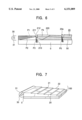
- FIG. 7 is a perspective view of a reflection type display device in accordance with the present invention.
- FIG. 7 is a schematic perspective view of a reflection type display device in accordance with the present invention, which includes a panel 0 and an illumination unit 100.
- the illumination unit 100 includes a light guide plate 20 and a light source 30.
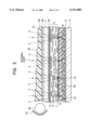
- FIG. 1 is a schematic representation showing a reflection type display device in accordance with the present invention. As shown in the drawing, the reflection type display device includes a panel 0, a light guide plate 20, and a light source 30 as fundamental components.
- the panel 0 includes a transparent first substrate 1 composed of, for example, glass, lying on the side of the external incident light, a second substrate 2 composed of, for example, glass, joined to the first substrate 1 with a predetermined gap therebetween and lying on the reflection side, and an electro-optical material 3a composed of, for example, a nematic liquid crystal, and an electrode (not shown in the drawing) composed of, for example, indium tin oxide (ITO), provided on at least one of the first substrate 1 and the second substrate 2 for applying a voltage to the electro-optical material 3a.
- micro-color filters of R, G, and B are provided on the side of the first substrate 1.
- a scattering type reflecting layer 8 composed of, for example, aluminum, is formed on the second substrate 2.
- the light guide plate 20 is placed external to the first substrate 1.
- the light source 30, for example, a cold cathode fluorescent tube, is placed at the end of the light guide plate 20 composed of an injection-molded piece of, for example, an acrylic resin, for generating illumination light as required.
- a reflecting mirror 31 is placed around the light source 30.
- the light guide plate 20, normally, transmits external light onto the panel 0 and emits the external light reflected from the panel 0, and, as required, guides illumination light onto the panel 0 and emits the illumination light reflected from the panel 0.
- the light guide plate 20 includes a planar section 22 divided into bands, and an inclined section 21 lying between the adjacent planar sections 22.
- the light guide plate 20 reflects the illumination light directed from the light source 30 at each inclined section 21 so as to guide it onto the first substrate 1, and emits the illumination light reflected from the second substrate 2 through each planar section 22 and inclined section 21.
- a width L1 of the planar section 22 is set at 15 or more times, or preferably at 20 or more times, a width L2 of the inclined section 21. That is, in the present invention, a width ratio between the planar section 22 and the inclined section 21 is set at 15 or more to 1, or preferably 20 or more to 1.
- the light entered into the panel 0 and reflected from the reflecting layer 8 reaches the viewer through the light guide plate 20. Most of the reflected light passes through the planar section 22, and only a little portion of the reflected light passes through the inclined section 21.
- a luminous energy ratio between the two is 15 or more to 1, or preferably 20 or more to 1, and the light passing through the inclined section 21 to be directed to the viewer can be reduced to such a degree that it is almost negligible. If no measures are taken with respect to the width ratio between the planar section 22 and the inclined section 21, a phenomenon of a double image occurs in which the pattern displayed on the panel 0 for the viewer is divided into two, i.e., a real image and a virtual image. In accordance with the present invention, this phenomenon can be effectively prevented.
- Table 1 shows the observations on a degree of a double image when the array pitch (L1+L2) of the light guide plate 20 is varied, with the width L2 of the inclined section 21 being fixed at 6 ⁇ m.
- the double image is weakened so as to be negligible.
- L1/L2 is 26.5.
- the array pitch (L1+L2) is 118 ⁇ m
- L1/L2 is 18.6 and the virtual image is slightly distinguishable.
- L1/L2 being 15 or more, the double image is practically suppressed, and preferably with L1/L2 being 20 or more, the double image is satisfactorily suppressed.
- FIG. 2 is a partial sectional view of a reflection type display device in accordance with the present invention when a light source 30 is turned on in a dark environment.
- the reflection type display device includes a panel 0, a light guide plate 20, a light source 30, and a polarizing plate 40 as fundamental components.
- the panel 0 includes a transparent first substrate 1 lying on the side of the external incident light, a second substrate 2 joined to the first substrate 1 with a predetermined gap therebetween and lying on the reflection side, an electro-optical material held between both substrates 1 and 2, and electrodes 10 and 11 provided on the first substrate 1 and the second substrate 2, respectively, for applying a voltage to the electro-optical material.
- the light guide plate 20 is composed of an injection-molded piece of a transparent material, for example, an acrylic resin, and is placed external to the first substrate 1 with the polarizing plate 40 therebetween.
- the light source 30 is placed at the end of the light guide plate 20, and generates illumination light as required.
- the light source 30 is composed of, for example, a cold cathode fluorescent tube, and is a so-called "edge light".
- a reflecting mirror 31 is provided behind the cylindrical light source 30.
- the light guide plate 20 normally transmits external light onto the first substrate 1 and emits the external light reflected from the second substrate 2, and also, as required, guides illumination light onto the first substrate 1 and emits the illumination light reflected from the second substrate 2.
- the thickness of the light guide plate 20 decreases from the end where the light source 30 lies toward the front. There is a difference in level between the adjacent planar sections 22, and an inclined section 21 is provided so as to connect the difference in level. The thickness of the light guide plate 20 decreases stepwise from the end where the light source 30 lies toward the front.
- the light guide plate 20 totally reflects the illumination light directed forward at each inclined section 21 so as to guide it onto the first substrate 1, and emits the illumination light reflected from the second substrate 2 through each planar section 22 and inclined section 21.
- the inclined section 21 of the light guide plate 20 is inclined at an angle of, for example, 45° in relation to the planar section 22. In the drawing, the angle of inclination is shown as ⁇ .
- the reflection type display device in use in a dark environment, and the light source 30 constituting the edge light is turned on.
- the illumination light radiating from the light source 30 illuminates the panel 0 through the light guide plate 20. That is, the illumination light advancing horizontally in the light guide plate 20 is totally reflected at the inclined section 21 and enters into the first substrate 1, while the illumination light reflected from the second substrate 2 is emitted through the planar section 22 and the inclined section 21 of the light guide plate 20.
- the width of the planar section 22 is set 15 or more times, or preferably, 20 or more times the width of the inclined section 21, the luminous energy of the light emitted from the inclined section 21 is relatively small, which is at a negligible level for the viewer. Therefore, a virtual image caused by the inclined section 21 is almost inconspicuous in comparison with a real image caused by the planar section 22, and thus the double image can be suppressed.
- the panel 0 uses a liquid crystal layer 3 mainly composed of nematic liquid crystal molecules 4 having positive dielectric anisotropy as an electro-optical material.
- the electro-optical material is not limited to a liquid crystal, and other materials may be used as the electro-optical material.
- a guest-host liquid crystal may be used instead of the nematic liquid crystal.
- the panel 0 is provided with a reflecting layer 8.
- the reflecting layer 8 lies on the side of the second substrate 2 for scattering and reflecting external light.
- the liquid crystal layer 3 is homogeneously aligned by upper and lower alignment layers 6 and 7. Electrodes 10 and 11 are formed on the first substrate 1 and the second substrate 2, respectively, for applying a voltage to the liquid crystal layer 3.
- the liquid crystal layer 3 is horizontally aligned in the absence of an applied voltage, and functions as a quarter-wavelength plate by appropriately setting the thickness. In the presence of an applied voltage, the liquid crystal molecules 4 are perpendicularly aligned and it loses the function as a quarter-wavelength plate. In this embodiment, a display is performed by combining the liquid crystal layer 3 which functions as a quarter-wavelength plate in response to an applied voltage with the polarizing plate 40.
- the reflecting layer 8 has a corrugated surface and scatters light. Accordingly, its paper-white appearance is suitable for the display background, and also, since it reflects the incident light with a relatively wide angle range, the viewing angle range is enlarged, and thus the display is easily viewed as well as the brightness of the display increasing.
- a transparent flattening layer 12 is provided between the reflecting layer 8 and the alignment layer 7 for compensating the corrugation.
- the reflecting layer 8 includes a resin layer 15 having a corrugation and a metal film 16 formed on the surface thereof, composed of, for example, aluminum.
- the resin layer 15 is a photosensitive resin layer on which the corrugation is patterned by means of photolithography.
- the photosensitive resin layer 15 is composed of, for example, a photo resist, and is applied on the entire surface of the substrate.
- the resin layer 15 is subjected to exposure treatment through a given mask, and is formed into, for example, a cylindrical pattern. Next, by heating to melt, the corrugation is formed stably.
- the metal film 16 composed of aluminum or the like having a predetermined thickness and a good reflectance is formed. If the depth of the corrugation is set at several ⁇ m, a good light scattering property is obtained and the reflecting layer 8 will have a white color.
- the flattening layer 12 is formed to compensate the corrugation.
- the flattening layer 12 is composed of a transparent organic substance such as an acrylic resin.
- the formation of the alignment layer 7 and rubbing treatment can be performed stably.
- the liquid crystal layer 3 is aligned homogeneously (horizontally) by the alignment layer 7 formed on the side of the second substrate 2 and the alignment layer 6 formed on the first substrate 1.
- the liquid crystal layer 3 may be aligned homeotropically (perpendicularly).
- nematic liquid crystal molecules 4 having negative dielectric anisotropy are used. The liquid crystal molecules 4 shift from the perpendicular alignment to the horizontal alignment in response to an applied voltage.
- micro-color filters of R, G, and B are provided on the first substrate 1 or the second substrate 2.
- the nematic liquid crystal molecules 4 are horizontally aligned, and the liquid crystal layer 3 functions as a quarter-wavelength plate.
- the illumination light radiating from the light source 30 is totally reflected at each inclined section 21 of the light guide plate 20 toward the polarizing plate 40.
- the illumination light is converted into a linearly polarized light by passing through the polarizing plate 40 and enters into the liquid crystal layer 3.
- the polarization axis (transmission axis) of the polarizing plate 40 is set at an angle of 45° in relation to the optic axis of the liquid crystal layer 3. Therefore, the linearly polarized light is converted into a circularly polarized light by passing through the liquid crystal layer 3.
- the circularly polarized light is reflected by the reflecting layer 8 and passes through the liquid crystal layer 3 in the reverse direction. As a result, the reflected circularly polarized light is converted into a linearly polarized light.
- the polarization axis of the reflected linearly polarized light is rotated by 90° from the incident linearly polarized light. Therefore, the reflected linearly polarized light cannot pass through the polarizing plate 40, resulting in a black display.
- the black-and-white display mode can be changed by switching on and off an applied voltage.
- FIG. 3 shows the reflection type display device shown in FIG. 2 in use in a bright environment.
- the display In a bright environment, because of an ample supply of external light such as natural light, the display is performed by making use of it. Therefore, the light source 30 is turned off. Thus, the electric power consumed by the display device as a whole can be reduced.
- the light guide plate 20 transmits the external light entering from the side of the viewer onto the first substrate 1, and emits the external light reflected from the second substrate 2 through the planar section 22 and the inclined section 21. Since the width of the planar section 22 is 15 or more times, or preferably 20 or more times, as large as the width of the inclined section 21, the light guide plate 20 does not hinder the viewer from seeing the display.
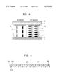
- FIG. 4 is a schematic diagram which illustrates the on-and-off mode of the reflection type display device shown in FIGS. 2 and 3.
- the left shows the ON state in which a white display is obtained.
- the right shows the OFF state in which a black display is obtained.
- the polarizing plate 40, the first substrate 1, the electrode 10, the liquid crystal layer 3, the electrode 11, the reflecting layer 8, and the second substrate 2 are deposited in that order from the top.
- the nematic liquid crystal molecules 4 are horizontally aligned, and the liquid crystal layer 3 functions as a quarter-wavelength plate.
- the liquid crystal molecules 4 changes from the horizontal alignment to a perpendicular alignment, and the liquid crystal layer 3 loses the function as a quarter-wavelength plate.
- the linearly polarized light passing through the polarizing plate 40 is converted into circularly polarized light by the liquid crystal layer 3, and is reflected by the reflecting layer 8.
- the reflected circularly polarized light is converted into an outgoing linearly polarized light by the liquid crystal layer 3. Since the polarization axis of the incident polarized light is orthogonal to that of the outgoing linearly polarized light, the outgoing linearly polarized light is absorbed by the polarizing plate 40, resulting in a black display.
- the liquid crystal layer 3 does not function as a quarter-wavelength plate, the incident linearly polarized light passing through the polarizing plate 40 is not affected by the liquid crystal layer 3, and passes though the polarizing plate 40 as an outgoing linearly polarized light, resulting in a white display.
- the contrast ratio between the white display and the black display is 15 or less. Accordingly, by setting the above-mentioned intensity ratio between the real image and the virtual image caused by the difference in refraction in the light guide plate so as to exceed the contrast ratio, the virtual image is substantially almost inconspicuous.
- the relative ratio between the width of the planar section and that of the inclined section is set at 15 or more such that the ratio between the quantity of the illumination light emitting from the planar section of the light guide plate and the quantity of the illumination light emitting from the inclined section exceeds the contrast ratio of 15 of the panel.
- FIG. 5 is a partial sectional view of a light guide plate in a reflection type display device as another embodiment of the present invention.
- a groove 20a is provided so as to isolate the adjacent planar sections 220, and an inclined section 211 is formed on the groove 20a.
- a vertical section 212 is also formed so as to face the inclined section 211.
- the inclined section 211 and the vertical section 212 are connected to each other by a bottom 213.
- the width of the planar section 220 is set, for example, at 201 ⁇ m
- the width of the inclined section is set, for example, at 6 ⁇ m
- the angle of inclination is set, for example, at 58°.
- the height of the vertical section 212 is set, for example, at 8.2 ⁇ m
- the width of the bottom 213 is set, for example, at 2 ⁇ m.
- FIG. 6 is a schematic diagram which illustrates the usage and the function of the light guide plate 20 shown in FIG. 5.
- the light guide plate 20 is joined to the panel 0 with an intervening layer 50 therebetween.
- a light source 30 is placed at the end of the light guide plate 20.
- the light source 30 is partially covered with a reflecting mirror 31.
- the light guide plate 20 includes the planar section 220 divided into bands and the groove 20a lying between the planar sections.
- the planar section 220 constitutes a light-emitting plane, and the groove 20a has the inclined section 211, the vertical section 212, and the bottom 213.
- the inclined section 211 totally reflects a portion of illumination light guided from the light source 30 onto the panel 0.
- the illumination light having different angles of incidence P1 is totally reflected by the inclined section 211 and enters into the panel 0 as illumination light P3.
- the vertical section 212 reenters illumination light P2 passing through the inclined section 211, which is the rest of the illumination light, into the light guide plate 20.
- the reentered illumination light is represented as P4.
- the planar section 220 emits the illumination light reflected from the panel 0.
- the angle of inclination of the planar section 220 in relation to the panel 0 is set small so that the display appearance viewed from the front of the panel 0 is not substantially changed. For example, the angle of inclination is approximately 20°.
- the inclined section 211 totally reflects the illumination light P1 guided from the light source 30, and also, the angle of inclination is set so that most of the illumination light reflected from the panel 0 can be totally reflected on the side of the light source 30.
- the angle of inclination is 58°.
- the angle of inclination of the vertical section 212 is larger than that of the opposing inclined section 211, and the reentered illumination light P4 passing through the inclined section 211 can be totally reflected within the light guide plate 20.
- the light guide plate 20 and the panel 0 are joined to each other with the intervening layer 50 therebetween, and by appropriately setting the refractive index of the intervening layer 50, the total reflection of the illumination light P4 at the interface between the light guide plate 20 and the panel 0 is achieved.
- the illumination light radiating from the light source 30 can be guided to a greater distance, resulting in uniform illumination.
- a light guide plate is placed on a reflection type panel, and a light source used as an auxiliary is placed at the end of the light guide plate.
- the light guide plate normally transmits external light onto the panel and emits the light reflected from the panel, and also, as required, guides illumination light onto the panel and emits the illumination light reflected from the panel. In a dark environment, the image can be viewed even in the reflection type panel by turning on the light source. On the other hand, in a bright environment where an ample supply of external light is available, the electric power is saved by turning off the light source.
- the light guide plate includes a planar section divided into bands and an inclined section lying between each band of the planar section.
- the light guide plate reflects the illumination light guided from the light source at each inclined section so as to guide it onto the first substrate, and emits the illumination light reflected from the second substrate through each planar section and inclined section.
- the width of the planar section is set at 15 or more times, or preferably at 20 or more times, the width of the inclined section.
Abstract
Description
I=I0×L2/(L1+L2)
              TABLE 1
______________________________________
                   Width of virtual
                                Intensity of
  L1 + L2 L1/L2 image virtual image
______________________________________
70.4 μm
        10.7       approximately 2 mm
                                Strong
  118 μm 18.6 approximately 2 mm Weak
  165 μm 26.5 approximately 2 mm Negligible
  254 μm 41.3 approximately 2 mm Negligible
  354 μm 58.0 approximately 2 mm Negligible
______________________________________
Claims (11)
Priority Applications (1)
| Application Number | Priority Date | Filing Date | Title |
|---|---|---|---|
| US09/233,519 US6151089A (en) | 1998-01-20 | 1999-01-20 | Reflection type display with light waveguide with inclined and planar surface sections |
Applications Claiming Priority (4)
| Application Number | Priority Date | Filing Date | Title |
|---|---|---|---|
| JP10022681A JPH11202785A (en) | 1998-01-20 | 1998-01-20 | Reflection type display device |
| JP10-022681 | 1998-01-20 | ||
| US09/046,765 US6266108B1 (en) | 1997-03-25 | 1998-03-24 | Reflective liquid crystal display device with a panel, a light guide plate and polarizing plate |
| US09/233,519 US6151089A (en) | 1998-01-20 | 1999-01-20 | Reflection type display with light waveguide with inclined and planar surface sections |
Related Parent Applications (1)
| Application Number | Title | Priority Date | Filing Date |
|---|---|---|---|
| US09/046,765 Continuation-In-Part US6266108B1 (en) | 1997-03-25 | 1998-03-24 | Reflective liquid crystal display device with a panel, a light guide plate and polarizing plate |
Publications (1)
| Publication Number | Publication Date |
|---|---|
| US6151089A true US6151089A (en) | 2000-11-21 |
Family
ID=26359939
Family Applications (1)
| Application Number | Title | Priority Date | Filing Date |
|---|---|---|---|
| US09/233,519 Expired - Fee Related US6151089A (en) | 1998-01-20 | 1999-01-20 | Reflection type display with light waveguide with inclined and planar surface sections |
Country Status (1)
| Country | Link |
|---|---|
| US (1) | US6151089A (en) |
Cited By (88)
| Publication number | Priority date | Publication date | Assignee | Title |
|---|---|---|---|---|
| US6243150B1 (en) * | 1998-03-26 | 2001-06-05 | Alps Electric Co., Ltd | Liquid crystal display device |
| US6323919B1 (en) * | 1998-10-02 | 2001-11-27 | Sony Corporation | Reflection type display with front light |
| US6407785B1 (en) * | 1998-10-05 | 2002-06-18 | Semiconductor Energy Laboratory Co., Ltd. | Reflection type semiconductor display device having optical fiber adjacent the surface of the main body |
| US6507378B1 (en) * | 1998-05-11 | 2003-01-14 | Nitto Denki Corporation | Reflection type liquid-crystal display unit |
| US6538711B2 (en) | 1998-07-31 | 2003-03-25 | Hitachi, Ltd. | Method of manufacturing reflective liquid crystal display device |
| US6585386B1 (en) * | 1998-04-14 | 2003-07-01 | Nitto Denko Corporation | Light pipe, surface light source device and reflection type liquid-crystal display device |
| US6590625B1 (en) * | 1999-05-24 | 2003-07-08 | Nitto Denko Corporation | Liquid-crystal display device |
| US6628352B1 (en) * | 1998-04-17 | 2003-09-30 | Sharp Kabushiki Kaisha | Liquid crystal display apparatus and electronic device incorporating the same wherein the optical guide having particular periodic structure |
| US6657684B2 (en) * | 2001-08-23 | 2003-12-02 | Seiko Epson Corporation | Reflective LCD with reflector having particular direction to illumination device |
| US6665029B2 (en) * | 2000-11-08 | 2003-12-16 | Nitto Denko Corporation | Optical path changing film and reflective liquid-crystal display device including same |
| US6686982B1 (en) * | 1999-04-13 | 2004-02-03 | Alps Electric Co., Ltd. | Reflection type liquid crystal display device in which oblique moiré fringe is not easily viewed and which is superior in display quality |
| US6738116B2 (en) * | 2000-12-01 | 2004-05-18 | Mitsubishi Denki Kabushiki Kaisha | Reflective liquid crystal display device |
| US20040105247A1 (en) * | 2002-12-03 | 2004-06-03 | Calvin Nate Howard | Diffusing backlight assembly |
| US6791635B1 (en) * | 1998-03-26 | 2004-09-14 | Enplas Corporation | Surface light source device of side light type and liquid crystal display |
| US6801184B2 (en) * | 2000-07-06 | 2004-10-05 | Benq Corporation | Backlight device |
| US6825899B2 (en) * | 2000-02-29 | 2004-11-30 | Alps Electric Co., Ltd. | Liquid crystal display device in which generation of moire fringes is prevented |
| US20060001036A1 (en) * | 2004-07-02 | 2006-01-05 | Gelcore, Llc | LED-based edge lit illumination system |
| US20060038769A1 (en) * | 2002-09-18 | 2006-02-23 | Koninklijke Philips Electronics N.V. | Display apparatus with scanning backlight |
| US7012660B1 (en) * | 1999-04-20 | 2006-03-14 | Nitto Denko Corporation | Liquid-crystal display device and light pipe |
| US20070019141A1 (en) * | 2004-12-28 | 2007-01-25 | Yuko Kizu | Liquid crystal display |
| US20070030696A1 (en) * | 2005-08-08 | 2007-02-08 | Innolux Display Corp. | Backlight module having interconnected light guide plate and light source cover |
| US7259806B1 (en) * | 1999-08-07 | 2007-08-21 | Lg.Philips Lcd Co., Ltd. | Liquid crystal display device with light absorbing layers |
| US20090063897A1 (en) * | 2002-02-14 | 2009-03-05 | Gravic, Inc. | Method of increasing system availability by assigning process pairs to processor pairs |
| US20090071594A1 (en) * | 2001-04-06 | 2009-03-19 | Ebert Composites Corporation | Method of Inserting Z-Axis Reinforcing Fibers into a Composite Laminate |
| US20090147535A1 (en) * | 2007-12-07 | 2009-06-11 | Qualcomm Incorporated | Light illumination of displays with front light guide and coupling elements |
| US7664350B2 (en) | 2007-09-10 | 2010-02-16 | Banyan Energy, Inc. | Compact optics for concentration, aggregation and illumination of light energy |
| US7672549B2 (en) | 2007-09-10 | 2010-03-02 | Banyan Energy, Inc. | Solar energy concentrator |
| US20100097897A1 (en) * | 2002-11-04 | 2010-04-22 | Tseng-Lu Chien | Time piece with led light means |
| US20100135038A1 (en) * | 2008-11-30 | 2010-06-03 | Handschy Mark A | Frontlights for reflective displays |
| US7750886B2 (en) | 2004-09-27 | 2010-07-06 | Qualcomm Mems Technologies, Inc. | Methods and devices for lighting displays |
| US7766498B2 (en) | 2006-06-21 | 2010-08-03 | Qualcomm Mems Technologies, Inc. | Linear solid state illuminator |
| US7777954B2 (en) | 2007-01-30 | 2010-08-17 | Qualcomm Mems Technologies, Inc. | Systems and methods of providing a light guiding layer |
| US7785693B2 (en) | 2001-04-06 | 2010-08-31 | Ebert Composites Corporation | Composite laminate structure |
| EP2251731A1 (en) * | 2004-09-27 | 2010-11-17 | Qualcomm Mems Technologies, Inc. | System and method of illuminating interferometric modulators using backlighting |
| US20100297365A1 (en) * | 2009-05-22 | 2010-11-25 | Curd Alistair P | Optical structure to reduce internal reflections |
| US7845841B2 (en) | 2006-08-28 | 2010-12-07 | Qualcomm Mems Technologies, Inc. | Angle sweeping holographic illuminator |
| US20100309540A1 (en) * | 1994-05-05 | 2010-12-09 | Qualcomm Mems Technologies, Inc. | Method and device for providing illumination to interferometric modulators |
| US7855827B2 (en) | 2006-10-06 | 2010-12-21 | Qualcomm Mems Technologies, Inc. | Internal optical isolation structure for integrated front or back lighting |
| US7864395B2 (en) | 2006-10-27 | 2011-01-04 | Qualcomm Mems Technologies, Inc. | Light guide including optical scattering elements and a method of manufacture |
| US7880954B2 (en) | 2004-03-05 | 2011-02-01 | Qualcomm Mems Technologies, Inc. | Integrated modulator illumination |
| CN101965478A (en) * | 2009-04-08 | 2011-02-02 | 松下电器产业株式会社 | Flat lighting device and liquid crystal display device using same |
| US7907319B2 (en) | 1995-11-06 | 2011-03-15 | Qualcomm Mems Technologies, Inc. | Method and device for modulating light with optical compensation |
| US7933475B2 (en) | 2006-02-17 | 2011-04-26 | Qualcomm Mems Technologies, Inc. | Method and apparatus for providing back-lighting in a display device |
| US7986451B2 (en) | 2004-09-27 | 2011-07-26 | Qualcomm Mems Technologies, Inc. | Optical films for directing light towards active areas of displays |
| US8040589B2 (en) | 2008-02-12 | 2011-10-18 | Qualcomm Mems Technologies, Inc. | Devices and methods for enhancing brightness of displays using angle conversion layers |
| US8045252B2 (en) | 2004-02-03 | 2011-10-25 | Qualcomm Mems Technologies, Inc. | Spatial light modulator with integrated optical compensation structure |
| US8049951B2 (en) | 2008-04-15 | 2011-11-01 | Qualcomm Mems Technologies, Inc. | Light with bi-directional propagation |
| US8061882B2 (en) | 2006-10-06 | 2011-11-22 | Qualcomm Mems Technologies, Inc. | Illumination device with built-in light coupler |
| US8107155B2 (en) | 2006-10-06 | 2012-01-31 | Qualcomm Mems Technologies, Inc. | System and method for reducing visual artifacts in displays |
| US8172417B2 (en) | 2009-03-06 | 2012-05-08 | Qualcomm Mems Technologies, Inc. | Shaped frontlight reflector for use with display |
| US8231257B2 (en) | 2009-01-13 | 2012-07-31 | Qualcomm Mems Technologies, Inc. | Large area light panel and screen |
| US8348489B2 (en) | 2008-01-30 | 2013-01-08 | Qualcomm Mems Technologies, Inc. | Thin illumination system |
| US8402647B2 (en) | 2010-08-25 | 2013-03-26 | Qualcomm Mems Technologies Inc. | Methods of manufacturing illumination systems |
| US8412010B2 (en) | 2007-09-10 | 2013-04-02 | Banyan Energy, Inc. | Compact optics for concentration and illumination systems |
| US8654061B2 (en) | 2008-02-12 | 2014-02-18 | Qualcomm Mems Technologies, Inc. | Integrated front light solution |
| US8674616B2 (en) | 2008-10-10 | 2014-03-18 | Qualcomm Mems Technologies, Inc. | Distributed illumination system |
| US8705914B2 (en) | 2007-09-10 | 2014-04-22 | Banyan Energy, Inc. | Redirecting optics for concentration and illumination systems |
| US8721149B2 (en) | 2008-01-30 | 2014-05-13 | Qualcomm Mems Technologies, Inc. | Illumination device having a tapered light guide |
| US8798425B2 (en) | 2007-12-07 | 2014-08-05 | Qualcomm Mems Technologies, Inc. | Decoupled holographic film and diffuser |
| US20140300838A1 (en) * | 2013-04-03 | 2014-10-09 | Delta Electronics, Inc. | Light Modulating Module and Image Display |
| US8872085B2 (en) | 2006-10-06 | 2014-10-28 | Qualcomm Mems Technologies, Inc. | Display device having front illuminator with turning features |
| US8902484B2 (en) | 2010-12-15 | 2014-12-02 | Qualcomm Mems Technologies, Inc. | Holographic brightness enhancement film |
| US8928967B2 (en) | 1998-04-08 | 2015-01-06 | Qualcomm Mems Technologies, Inc. | Method and device for modulating light |
| US8941631B2 (en) | 2007-11-16 | 2015-01-27 | Qualcomm Mems Technologies, Inc. | Simultaneous light collection and illumination on an active display |
| US8971675B2 (en) | 2006-01-13 | 2015-03-03 | Qualcomm Mems Technologies, Inc. | Interconnect structure for MEMS device |
| US8979349B2 (en) | 2009-05-29 | 2015-03-17 | Qualcomm Mems Technologies, Inc. | Illumination devices and methods of fabrication thereof |
| US9019183B2 (en) | 2006-10-06 | 2015-04-28 | Qualcomm Mems Technologies, Inc. | Optical loss structure integrated in an illumination apparatus |
| US9025235B2 (en) | 2002-12-25 | 2015-05-05 | Qualcomm Mems Technologies, Inc. | Optical interference type of color display having optical diffusion layer between substrate and electrode |
| US20150124316A1 (en) * | 2013-07-10 | 2015-05-07 | Boe Technology Group Co., Ltd. | Stereoscopic display device |
| US9110289B2 (en) | 1998-04-08 | 2015-08-18 | Qualcomm Mems Technologies, Inc. | Device for modulating light with multiple electrodes |
| US9291320B2 (en) | 2013-01-30 | 2016-03-22 | Cree, Inc. | Consolidated troffer |
| US9366799B2 (en) | 2013-03-15 | 2016-06-14 | Cree, Inc. | Optical waveguide bodies and luminaires utilizing same |
| US9366396B2 (en) | 2013-01-30 | 2016-06-14 | Cree, Inc. | Optical waveguide and lamp including same |
| US9389367B2 (en) | 2013-01-30 | 2016-07-12 | Cree, Inc. | Optical waveguide and luminaire incorporating same |
| US9442243B2 (en) | 2013-01-30 | 2016-09-13 | Cree, Inc. | Waveguide bodies including redirection features and methods of producing same |
| US9625638B2 (en) | 2013-03-15 | 2017-04-18 | Cree, Inc. | Optical waveguide body |
| US9690029B2 (en) | 2013-01-30 | 2017-06-27 | Cree, Inc. | Optical waveguides and luminaires incorporating same |
| US9798072B2 (en) | 2013-03-15 | 2017-10-24 | Cree, Inc. | Optical element and method of forming an optical element |
| US9869432B2 (en) | 2013-01-30 | 2018-01-16 | Cree, Inc. | Luminaires using waveguide bodies and optical elements |
| US9920901B2 (en) | 2013-03-15 | 2018-03-20 | Cree, Inc. | LED lensing arrangement |
| US10209429B2 (en) | 2013-03-15 | 2019-02-19 | Cree, Inc. | Luminaire with selectable luminous intensity pattern |
| US20190121171A1 (en) * | 2017-03-02 | 2019-04-25 | Boe Technology Group Co., Ltd. | Liquid crystal display panel, liquid crystal display device and display method thereof |
| US10416377B2 (en) | 2016-05-06 | 2019-09-17 | Cree, Inc. | Luminaire with controllable light emission |
| US10436970B2 (en) | 2013-03-15 | 2019-10-08 | Ideal Industries Lighting Llc | Shaped optical waveguide bodies |
| US11112083B2 (en) | 2013-03-15 | 2021-09-07 | Ideal Industries Lighting Llc | Optic member for an LED light fixture |
| US11378839B2 (en) * | 2020-07-20 | 2022-07-05 | Boe Technology Group Co., Ltd. | Transparent display panel, preparation method thereof and display device |
| US11474388B2 (en) * | 2020-07-15 | 2022-10-18 | Sichuan Longhua Film Co. Ltd. | Display panel and rollable display device |
| US11719882B2 (en) | 2016-05-06 | 2023-08-08 | Ideal Industries Lighting Llc | Waveguide-based light sources with dynamic beam shaping |
Citations (12)
| Publication number | Priority date | Publication date | Assignee | Title |
|---|---|---|---|---|
| US4914553A (en) * | 1984-07-26 | 1990-04-03 | Sharp Kabushiki Kaisha | Lighting device |
| US5050946A (en) * | 1990-09-27 | 1991-09-24 | Compaq Computer Corporation | Faceted light pipe |
| US5341231A (en) * | 1991-12-03 | 1994-08-23 | Sharp Kabushiki Kaisha | Liquid crystal display device with edge lit lightguide reflecting light to back reflector by total internal reflection |
| US5485354A (en) * | 1993-09-09 | 1996-01-16 | Precision Lamp, Inc. | Flat panel display lighting system |
| US5489999A (en) * | 1993-07-27 | 1996-02-06 | Sharp Kabushiki Kaisha | Liquid crystal display device having a circuit board disposed at a recess of a light guide plate |
| US5587816A (en) * | 1992-10-09 | 1996-12-24 | Asahi Glass Company Ltd. | LCD device including an illumination device having a polarized light separating sheet between a light guide and the display |
| US5608550A (en) * | 1994-06-24 | 1997-03-04 | Minnesota Mining And Manufacturing Company | Front-lit liquid crystal display having brightness enhancing film with microridges which directs light through the display to a reflector |
| US5703667A (en) * | 1996-05-31 | 1997-12-30 | Shimada Precision, Co., Ltd. | Light guide plates and light guide plate assembly utilizing diffraction grating |
| US5830542A (en) * | 1996-07-15 | 1998-11-03 | Sony Corporation | Reflective guest-host liquid-crystal display |
| US5838403A (en) * | 1996-02-14 | 1998-11-17 | Physical Optics Corporation | Liquid crystal display system with internally reflecting waveguide for backlighting and non-Lambertian diffusing |
| US5914760A (en) * | 1996-06-21 | 1999-06-22 | Casio Computer Co., Ltd. | Surface light source device and liquid crystal display device using the same |
| US5917565A (en) * | 1995-02-28 | 1999-06-29 | International Business Machines Corporation | Apparatus for increasing a polarization component, light guide unit, liquid crystal display and polarization method |
-
1999
- 1999-01-20 US US09/233,519 patent/US6151089A/en not_active Expired - Fee Related
Patent Citations (12)
| Publication number | Priority date | Publication date | Assignee | Title |
|---|---|---|---|---|
| US4914553A (en) * | 1984-07-26 | 1990-04-03 | Sharp Kabushiki Kaisha | Lighting device |
| US5050946A (en) * | 1990-09-27 | 1991-09-24 | Compaq Computer Corporation | Faceted light pipe |
| US5341231A (en) * | 1991-12-03 | 1994-08-23 | Sharp Kabushiki Kaisha | Liquid crystal display device with edge lit lightguide reflecting light to back reflector by total internal reflection |
| US5587816A (en) * | 1992-10-09 | 1996-12-24 | Asahi Glass Company Ltd. | LCD device including an illumination device having a polarized light separating sheet between a light guide and the display |
| US5489999A (en) * | 1993-07-27 | 1996-02-06 | Sharp Kabushiki Kaisha | Liquid crystal display device having a circuit board disposed at a recess of a light guide plate |
| US5485354A (en) * | 1993-09-09 | 1996-01-16 | Precision Lamp, Inc. | Flat panel display lighting system |
| US5608550A (en) * | 1994-06-24 | 1997-03-04 | Minnesota Mining And Manufacturing Company | Front-lit liquid crystal display having brightness enhancing film with microridges which directs light through the display to a reflector |
| US5917565A (en) * | 1995-02-28 | 1999-06-29 | International Business Machines Corporation | Apparatus for increasing a polarization component, light guide unit, liquid crystal display and polarization method |
| US5838403A (en) * | 1996-02-14 | 1998-11-17 | Physical Optics Corporation | Liquid crystal display system with internally reflecting waveguide for backlighting and non-Lambertian diffusing |
| US5703667A (en) * | 1996-05-31 | 1997-12-30 | Shimada Precision, Co., Ltd. | Light guide plates and light guide plate assembly utilizing diffraction grating |
| US5914760A (en) * | 1996-06-21 | 1999-06-22 | Casio Computer Co., Ltd. | Surface light source device and liquid crystal display device using the same |
| US5830542A (en) * | 1996-07-15 | 1998-11-03 | Sony Corporation | Reflective guest-host liquid-crystal display |
Cited By (129)
| Publication number | Priority date | Publication date | Assignee | Title |
|---|---|---|---|---|
| US8054532B2 (en) | 1994-05-05 | 2011-11-08 | Qualcomm Mems Technologies, Inc. | Method and device for providing illumination to interferometric modulators |
| US20100309540A1 (en) * | 1994-05-05 | 2010-12-09 | Qualcomm Mems Technologies, Inc. | Method and device for providing illumination to interferometric modulators |
| US7907319B2 (en) | 1995-11-06 | 2011-03-15 | Qualcomm Mems Technologies, Inc. | Method and device for modulating light with optical compensation |
| US6930735B2 (en) | 1998-03-26 | 2005-08-16 | Enplas Corporation | Surface light source device of side light type and liquid crystal display |
| US6791635B1 (en) * | 1998-03-26 | 2004-09-14 | Enplas Corporation | Surface light source device of side light type and liquid crystal display |
| US6243150B1 (en) * | 1998-03-26 | 2001-06-05 | Alps Electric Co., Ltd | Liquid crystal display device |
| US9110289B2 (en) | 1998-04-08 | 2015-08-18 | Qualcomm Mems Technologies, Inc. | Device for modulating light with multiple electrodes |
| US8928967B2 (en) | 1998-04-08 | 2015-01-06 | Qualcomm Mems Technologies, Inc. | Method and device for modulating light |
| US6585386B1 (en) * | 1998-04-14 | 2003-07-01 | Nitto Denko Corporation | Light pipe, surface light source device and reflection type liquid-crystal display device |
| US6882381B2 (en) | 1998-04-17 | 2005-04-19 | Sharp Kabushiki Kaisha | Liquid crystal display apparatus and electronic device incorporating the same |
| US20040061818A1 (en) * | 1998-04-17 | 2004-04-01 | Sharp Kabushiki Kaisha | Liquid crystal display apparatus and electronic device incorporating the same |
| US6628352B1 (en) * | 1998-04-17 | 2003-09-30 | Sharp Kabushiki Kaisha | Liquid crystal display apparatus and electronic device incorporating the same wherein the optical guide having particular periodic structure |
| US6507378B1 (en) * | 1998-05-11 | 2003-01-14 | Nitto Denki Corporation | Reflection type liquid-crystal display unit |
| US6538711B2 (en) | 1998-07-31 | 2003-03-25 | Hitachi, Ltd. | Method of manufacturing reflective liquid crystal display device |
| US6323919B1 (en) * | 1998-10-02 | 2001-11-27 | Sony Corporation | Reflection type display with front light |
| US20040257503A1 (en) * | 1998-10-05 | 2004-12-23 | Shunpei Yamazaki | Reflection type semiconductor display device |
| US6999137B2 (en) * | 1998-10-05 | 2006-02-14 | Semiconductor Energy Laboratory Co., Ltd. | Reflection type semiconductor display device |
| US20060092354A1 (en) * | 1998-10-05 | 2006-05-04 | Semiconductor Energy Laboratory Co., Ltd. | Reflection type semiconductor display device |
| US6407785B1 (en) * | 1998-10-05 | 2002-06-18 | Semiconductor Energy Laboratory Co., Ltd. | Reflection type semiconductor display device having optical fiber adjacent the surface of the main body |
| US7253854B2 (en) * | 1998-10-05 | 2007-08-07 | Semiconductor Energy Laboratory Co., Ltd. | Reflection type semiconductor display device |
| US6784952B2 (en) | 1998-10-05 | 2004-08-31 | Semiconductor Energy Laboratory Co., Ltd. | Reflection type semiconductor display device |
| US20020176035A1 (en) * | 1998-10-05 | 2002-11-28 | Semiconductor Energy Laboratory Co., Ltd. | Reflection type semiconductor display device |
| US6686982B1 (en) * | 1999-04-13 | 2004-02-03 | Alps Electric Co., Ltd. | Reflection type liquid crystal display device in which oblique moiré fringe is not easily viewed and which is superior in display quality |
| US7012660B1 (en) * | 1999-04-20 | 2006-03-14 | Nitto Denko Corporation | Liquid-crystal display device and light pipe |
| US6590625B1 (en) * | 1999-05-24 | 2003-07-08 | Nitto Denko Corporation | Liquid-crystal display device |
| US7259806B1 (en) * | 1999-08-07 | 2007-08-21 | Lg.Philips Lcd Co., Ltd. | Liquid crystal display device with light absorbing layers |
| US6825899B2 (en) * | 2000-02-29 | 2004-11-30 | Alps Electric Co., Ltd. | Liquid crystal display device in which generation of moire fringes is prevented |
| US20040212581A1 (en) * | 2000-07-06 | 2004-10-28 | Acer Communications And Multimedia Inc. | Backlight device |
| US7154469B2 (en) | 2000-07-06 | 2006-12-26 | Acer Communications And Multimedia Inc. | Backlight device |
| US6801184B2 (en) * | 2000-07-06 | 2004-10-05 | Benq Corporation | Backlight device |
| US6665029B2 (en) * | 2000-11-08 | 2003-12-16 | Nitto Denko Corporation | Optical path changing film and reflective liquid-crystal display device including same |
| US6738116B2 (en) * | 2000-12-01 | 2004-05-18 | Mitsubishi Denki Kabushiki Kaisha | Reflective liquid crystal display device |
| US20090071594A1 (en) * | 2001-04-06 | 2009-03-19 | Ebert Composites Corporation | Method of Inserting Z-Axis Reinforcing Fibers into a Composite Laminate |
| US7785693B2 (en) | 2001-04-06 | 2010-08-31 | Ebert Composites Corporation | Composite laminate structure |
| US6657684B2 (en) * | 2001-08-23 | 2003-12-02 | Seiko Epson Corporation | Reflective LCD with reflector having particular direction to illumination device |
| US20090063897A1 (en) * | 2002-02-14 | 2009-03-05 | Gravic, Inc. | Method of increasing system availability by assigning process pairs to processor pairs |
| US20060038769A1 (en) * | 2002-09-18 | 2006-02-23 | Koninklijke Philips Electronics N.V. | Display apparatus with scanning backlight |
| US8164984B2 (en) * | 2002-11-04 | 2012-04-24 | Tseng-Lu Chien | Time piece with LED light means |
| US20100097897A1 (en) * | 2002-11-04 | 2010-04-22 | Tseng-Lu Chien | Time piece with led light means |
| US20040105247A1 (en) * | 2002-12-03 | 2004-06-03 | Calvin Nate Howard | Diffusing backlight assembly |
| US9025235B2 (en) | 2002-12-25 | 2015-05-05 | Qualcomm Mems Technologies, Inc. | Optical interference type of color display having optical diffusion layer between substrate and electrode |
| US8045252B2 (en) | 2004-02-03 | 2011-10-25 | Qualcomm Mems Technologies, Inc. | Spatial light modulator with integrated optical compensation structure |
| US9019590B2 (en) | 2004-02-03 | 2015-04-28 | Qualcomm Mems Technologies, Inc. | Spatial light modulator with integrated optical compensation structure |
| US8111445B2 (en) | 2004-02-03 | 2012-02-07 | Qualcomm Mems Technologies, Inc. | Spatial light modulator with integrated optical compensation structure |
| US7880954B2 (en) | 2004-03-05 | 2011-02-01 | Qualcomm Mems Technologies, Inc. | Integrated modulator illumination |
| US20060001036A1 (en) * | 2004-07-02 | 2006-01-05 | Gelcore, Llc | LED-based edge lit illumination system |
| US8324640B2 (en) | 2004-07-02 | 2012-12-04 | GE Lighting Solutions, LLC | LED-based edge lit illumination system |
| EP2251731A1 (en) * | 2004-09-27 | 2010-11-17 | Qualcomm Mems Technologies, Inc. | System and method of illuminating interferometric modulators using backlighting |
| US8411026B2 (en) | 2004-09-27 | 2013-04-02 | Qualcomm Mems Technologies, Inc. | Methods and devices for lighting displays |
| US7750886B2 (en) | 2004-09-27 | 2010-07-06 | Qualcomm Mems Technologies, Inc. | Methods and devices for lighting displays |
| US8040588B2 (en) | 2004-09-27 | 2011-10-18 | Qualcomm Mems Technologies, Inc. | System and method of illuminating interferometric modulators using backlighting |
| US7986451B2 (en) | 2004-09-27 | 2011-07-26 | Qualcomm Mems Technologies, Inc. | Optical films for directing light towards active areas of displays |
| US20070019141A1 (en) * | 2004-12-28 | 2007-01-25 | Yuko Kizu | Liquid crystal display |
| US7375783B2 (en) * | 2004-12-28 | 2008-05-20 | Kabushiki Kaisha Toshiba | Liquid crystal display |
| US20070030696A1 (en) * | 2005-08-08 | 2007-02-08 | Innolux Display Corp. | Backlight module having interconnected light guide plate and light source cover |
| US8971675B2 (en) | 2006-01-13 | 2015-03-03 | Qualcomm Mems Technologies, Inc. | Interconnect structure for MEMS device |
| US7933475B2 (en) | 2006-02-17 | 2011-04-26 | Qualcomm Mems Technologies, Inc. | Method and apparatus for providing back-lighting in a display device |
| US7766498B2 (en) | 2006-06-21 | 2010-08-03 | Qualcomm Mems Technologies, Inc. | Linear solid state illuminator |
| US7845841B2 (en) | 2006-08-28 | 2010-12-07 | Qualcomm Mems Technologies, Inc. | Angle sweeping holographic illuminator |
| US8061882B2 (en) | 2006-10-06 | 2011-11-22 | Qualcomm Mems Technologies, Inc. | Illumination device with built-in light coupler |
| US7855827B2 (en) | 2006-10-06 | 2010-12-21 | Qualcomm Mems Technologies, Inc. | Internal optical isolation structure for integrated front or back lighting |
| US9019183B2 (en) | 2006-10-06 | 2015-04-28 | Qualcomm Mems Technologies, Inc. | Optical loss structure integrated in an illumination apparatus |
| US8107155B2 (en) | 2006-10-06 | 2012-01-31 | Qualcomm Mems Technologies, Inc. | System and method for reducing visual artifacts in displays |
| US8872085B2 (en) | 2006-10-06 | 2014-10-28 | Qualcomm Mems Technologies, Inc. | Display device having front illuminator with turning features |
| US7864395B2 (en) | 2006-10-27 | 2011-01-04 | Qualcomm Mems Technologies, Inc. | Light guide including optical scattering elements and a method of manufacture |
| US7777954B2 (en) | 2007-01-30 | 2010-08-17 | Qualcomm Mems Technologies, Inc. | Systems and methods of providing a light guiding layer |
| US7925129B2 (en) | 2007-09-10 | 2011-04-12 | Banyan Energy, Inc. | Compact optics for concentration, aggregation and illumination of light energy |
| US9229144B2 (en) | 2007-09-10 | 2016-01-05 | Banyan Energy Inc. | Redirecting optics for concentration and illumination systems |
| US7664350B2 (en) | 2007-09-10 | 2010-02-16 | Banyan Energy, Inc. | Compact optics for concentration, aggregation and illumination of light energy |
| US7672549B2 (en) | 2007-09-10 | 2010-03-02 | Banyan Energy, Inc. | Solar energy concentrator |
| US8705914B2 (en) | 2007-09-10 | 2014-04-22 | Banyan Energy, Inc. | Redirecting optics for concentration and illumination systems |
| US8412010B2 (en) | 2007-09-10 | 2013-04-02 | Banyan Energy, Inc. | Compact optics for concentration and illumination systems |
| US8941631B2 (en) | 2007-11-16 | 2015-01-27 | Qualcomm Mems Technologies, Inc. | Simultaneous light collection and illumination on an active display |
| US8798425B2 (en) | 2007-12-07 | 2014-08-05 | Qualcomm Mems Technologies, Inc. | Decoupled holographic film and diffuser |
| US20090147535A1 (en) * | 2007-12-07 | 2009-06-11 | Qualcomm Incorporated | Light illumination of displays with front light guide and coupling elements |
| US7949213B2 (en) * | 2007-12-07 | 2011-05-24 | Qualcomm Mems Technologies, Inc. | Light illumination of displays with front light guide and coupling elements |
| US9395479B2 (en) | 2008-01-30 | 2016-07-19 | Qualcomm Mems Technologies, Inc. | Illumination device having a tapered light guide |
| US8348489B2 (en) | 2008-01-30 | 2013-01-08 | Qualcomm Mems Technologies, Inc. | Thin illumination system |
| US8721149B2 (en) | 2008-01-30 | 2014-05-13 | Qualcomm Mems Technologies, Inc. | Illumination device having a tapered light guide |
| US8740439B2 (en) | 2008-01-30 | 2014-06-03 | Qualcomm Mems Technologies, Inc. | Thin illumination system |
| US9244212B2 (en) | 2008-01-30 | 2016-01-26 | Qualcomm Mems Technologies, Inc. | Illumination device having a tapered light guide |
| US9448353B2 (en) | 2008-01-30 | 2016-09-20 | Qualcomm Mems Technologies, Inc. | Illumination device having a tapered light guide |
| US8040589B2 (en) | 2008-02-12 | 2011-10-18 | Qualcomm Mems Technologies, Inc. | Devices and methods for enhancing brightness of displays using angle conversion layers |
| US8654061B2 (en) | 2008-02-12 | 2014-02-18 | Qualcomm Mems Technologies, Inc. | Integrated front light solution |
| US8049951B2 (en) | 2008-04-15 | 2011-11-01 | Qualcomm Mems Technologies, Inc. | Light with bi-directional propagation |
| US8674616B2 (en) | 2008-10-10 | 2014-03-18 | Qualcomm Mems Technologies, Inc. | Distributed illumination system |
| US20100135038A1 (en) * | 2008-11-30 | 2010-06-03 | Handschy Mark A | Frontlights for reflective displays |
| US8439546B2 (en) | 2009-01-13 | 2013-05-14 | Qualcomm Mems Technologies, Inc. | Large area light panel and screen |
| US8231257B2 (en) | 2009-01-13 | 2012-07-31 | Qualcomm Mems Technologies, Inc. | Large area light panel and screen |
| US8172417B2 (en) | 2009-03-06 | 2012-05-08 | Qualcomm Mems Technologies, Inc. | Shaped frontlight reflector for use with display |
| CN101965478A (en) * | 2009-04-08 | 2011-02-02 | 松下电器产业株式会社 | Flat lighting device and liquid crystal display device using same |
| US20110058122A1 (en) * | 2009-04-08 | 2011-03-10 | Shinichi Shikii | Surface illumination apparatus and liquid crystal display using same |
| US8233113B2 (en) * | 2009-04-08 | 2012-07-31 | Panasonic Corporation | Surface illumination apparatus and liquid crystal display using same |
| US20100297365A1 (en) * | 2009-05-22 | 2010-11-25 | Curd Alistair P | Optical structure to reduce internal reflections |
| US8252390B2 (en) * | 2009-05-22 | 2012-08-28 | Sharp Kabushiki Kaisha | Optical structure to reduce internal reflections |
| US8979349B2 (en) | 2009-05-29 | 2015-03-17 | Qualcomm Mems Technologies, Inc. | Illumination devices and methods of fabrication thereof |
| US9121979B2 (en) | 2009-05-29 | 2015-09-01 | Qualcomm Mems Technologies, Inc. | Illumination devices and methods of fabrication thereof |
| US8402647B2 (en) | 2010-08-25 | 2013-03-26 | Qualcomm Mems Technologies Inc. | Methods of manufacturing illumination systems |
| US8902484B2 (en) | 2010-12-15 | 2014-12-02 | Qualcomm Mems Technologies, Inc. | Holographic brightness enhancement film |
| US9581751B2 (en) | 2013-01-30 | 2017-02-28 | Cree, Inc. | Optical waveguide and lamp including same |
| US9823408B2 (en) | 2013-01-30 | 2017-11-21 | Cree, Inc. | Optical waveguide and luminaire incorporating same |
| US10436969B2 (en) | 2013-01-30 | 2019-10-08 | Ideal Industries Lighting Llc | Optical waveguide and luminaire incorporating same |
| US9366396B2 (en) | 2013-01-30 | 2016-06-14 | Cree, Inc. | Optical waveguide and lamp including same |
| US9389367B2 (en) | 2013-01-30 | 2016-07-12 | Cree, Inc. | Optical waveguide and luminaire incorporating same |
| US9291320B2 (en) | 2013-01-30 | 2016-03-22 | Cree, Inc. | Consolidated troffer |
| US9442243B2 (en) | 2013-01-30 | 2016-09-13 | Cree, Inc. | Waveguide bodies including redirection features and methods of producing same |
| US11644157B2 (en) | 2013-01-30 | 2023-05-09 | Ideal Industries Lighting Llc | Luminaires using waveguide bodies and optical elements |
| US9519095B2 (en) | 2013-01-30 | 2016-12-13 | Cree, Inc. | Optical waveguides |
| US9869432B2 (en) | 2013-01-30 | 2018-01-16 | Cree, Inc. | Luminaires using waveguide bodies and optical elements |
| US9690029B2 (en) | 2013-01-30 | 2017-06-27 | Cree, Inc. | Optical waveguides and luminaires incorporating same |
| US9625638B2 (en) | 2013-03-15 | 2017-04-18 | Cree, Inc. | Optical waveguide body |
| US9798072B2 (en) | 2013-03-15 | 2017-10-24 | Cree, Inc. | Optical element and method of forming an optical element |
| US10436970B2 (en) | 2013-03-15 | 2019-10-08 | Ideal Industries Lighting Llc | Shaped optical waveguide bodies |
| US9920901B2 (en) | 2013-03-15 | 2018-03-20 | Cree, Inc. | LED lensing arrangement |
| US10209429B2 (en) | 2013-03-15 | 2019-02-19 | Cree, Inc. | Luminaire with selectable luminous intensity pattern |
| US11112083B2 (en) | 2013-03-15 | 2021-09-07 | Ideal Industries Lighting Llc | Optic member for an LED light fixture |
| US9366799B2 (en) | 2013-03-15 | 2016-06-14 | Cree, Inc. | Optical waveguide bodies and luminaires utilizing same |
| US20140300838A1 (en) * | 2013-04-03 | 2014-10-09 | Delta Electronics, Inc. | Light Modulating Module and Image Display |
| US9360678B2 (en) * | 2013-04-03 | 2016-06-07 | Delta Electronics, Inc. | Light modulating module and image display |
| US9891441B2 (en) * | 2013-07-10 | 2018-02-13 | Boe Technology Group Co., Ltd. | Stereoscopic display device |
| US20150124316A1 (en) * | 2013-07-10 | 2015-05-07 | Boe Technology Group Co., Ltd. | Stereoscopic display device |
| US10416377B2 (en) | 2016-05-06 | 2019-09-17 | Cree, Inc. | Luminaire with controllable light emission |
| US10527785B2 (en) | 2016-05-06 | 2020-01-07 | Ideal Industries Lighting Llc | Waveguide-based light sources with dynamic beam shaping |
| US10890714B2 (en) | 2016-05-06 | 2021-01-12 | Ideal Industries Lighting Llc | Waveguide-based light sources with dynamic beam shaping |
| US11372156B2 (en) | 2016-05-06 | 2022-06-28 | Ideal Industries Lighting Llc | Waveguide-based light sources with dynamic beam shaping |
| US11719882B2 (en) | 2016-05-06 | 2023-08-08 | Ideal Industries Lighting Llc | Waveguide-based light sources with dynamic beam shaping |
| US20190121171A1 (en) * | 2017-03-02 | 2019-04-25 | Boe Technology Group Co., Ltd. | Liquid crystal display panel, liquid crystal display device and display method thereof |
| US11474388B2 (en) * | 2020-07-15 | 2022-10-18 | Sichuan Longhua Film Co. Ltd. | Display panel and rollable display device |
| US11378839B2 (en) * | 2020-07-20 | 2022-07-05 | Boe Technology Group Co., Ltd. | Transparent display panel, preparation method thereof and display device |
Similar Documents
| Publication | Publication Date | Title |
|---|---|---|
| US6151089A (en) | Reflection type display with light waveguide with inclined and planar surface sections | |
| US6108059A (en) | Reflective display having a laminated structure of a polarizer and quarter wave plate being attached to a light guide plate | |
| US6266108B1 (en) | Reflective liquid crystal display device with a panel, a light guide plate and polarizing plate | |
| US6163351A (en) | Backlight for liquid crystal display apparatus and liquid crystal display apparatus incorporating the same | |
| US7301591B2 (en) | Liquid crystal display device wherein the number of light emitting elements activated differs depending on whether display is performed by the first or second liquid crystal panel | |
| US6554440B2 (en) | Light pipe, plane light source unit and liquid-crystal display device | |
| JP2000200049A (en) | Reflection type display device | |
| JP3506841B2 (en) | Illumination device of reflective liquid crystal display device and reflective liquid crystal display device | |
| JP3381133B2 (en) | Liquid crystal display | |
| US6735373B2 (en) | Plane light source unit and liquid-crystal display device | |
| US7327417B2 (en) | Display device | |
| US7084941B2 (en) | Liquid crystal display device | |
| JP4122555B2 (en) | Reflective display device | |
| JPH0675218A (en) | Liquid crystal panel | |
| JP2000147487A (en) | Liquid crystal display device | |
| WO1998032047A1 (en) | Ambient illuminated electro-optic display device | |
| US20090310071A1 (en) | Transreflective display panel and display apparatus including the same | |
| KR100783810B1 (en) | Liquid crystal display apparatus employing polymer dispersed liquid crystal mode | |
| KR100880217B1 (en) | A Back light | |
| JPH07333610A (en) | Illumination device and display device using the same | |
| JP2007004162A (en) | Display panel assembly and display apparatus having the same | |
| JPH11202785A (en) | Reflection type display device | |
| JP3807944B2 (en) | Display device and lighting device | |
| KR101281668B1 (en) | Reflective polarizing plate and liquid crystal display device having thereof | |
| KR20010051562A (en) | Light pipe, surface light source unit and reflection type liquid-crystal display device |
Legal Events
| Date | Code | Title | Description |
|---|---|---|---|
| AS | Assignment |
Owner name: SONY CORPORATION, JAPAN Free format text: ASSIGNMENT OF ASSIGNORS INTEREST;ASSIGNORS:YANG, YING BAO;URABE, TETSUO;KINOSHITA, YUKIO;AND OTHERS;REEL/FRAME:010391/0441;SIGNING DATES FROM 19990906 TO 19991001 |
|
| FPAY | Fee payment |
Year of fee payment: 4 |
|
| FPAY | Fee payment |
Year of fee payment: 8 |
|
| REMI | Maintenance fee reminder mailed | ||
| LAPS | Lapse for failure to pay maintenance fees | ||
| LAPS | Lapse for failure to pay maintenance fees |
Free format text: PATENT EXPIRED FOR FAILURE TO PAY MAINTENANCE FEES (ORIGINAL EVENT CODE: EXP.); ENTITY STATUS OF PATENT OWNER: LARGE ENTITY |
|
| STCH | Information on status: patent discontinuation |
Free format text: PATENT EXPIRED DUE TO NONPAYMENT OF MAINTENANCE FEES UNDER 37 CFR 1.362 |
|
| FP | Lapsed due to failure to pay maintenance fee |
Effective date: 20121121 |