US6151248A - Dual floating gate EEPROM cell array with steering gates shared by adjacent cells - Google Patents
Dual floating gate EEPROM cell array with steering gates shared by adjacent cells Download PDFInfo
- Publication number
- US6151248A US6151248A US09/343,328 US34332899A US6151248A US 6151248 A US6151248 A US 6151248A US 34332899 A US34332899 A US 34332899A US 6151248 A US6151248 A US 6151248A
- Authority
- US
- United States
- Prior art keywords
- gates
- gate
- floating
- steering
- substrate
- Prior art date
- Legal status (The legal status is an assumption and is not a legal conclusion. Google has not performed a legal analysis and makes no representation as to the accuracy of the status listed.)
- Expired - Lifetime
Links
Images

Classifications
-
- G—PHYSICS
- G11—INFORMATION STORAGE
- G11C—STATIC STORES
- G11C16/00—Erasable programmable read-only memories
- G11C16/02—Erasable programmable read-only memories electrically programmable
- G11C16/04—Erasable programmable read-only memories electrically programmable using variable threshold transistors, e.g. FAMOS
- G11C16/0466—Erasable programmable read-only memories electrically programmable using variable threshold transistors, e.g. FAMOS comprising cells with charge storage in an insulating layer, e.g. metal-nitride-oxide-silicon [MNOS], silicon-oxide-nitride-oxide-silicon [SONOS]
- G11C16/0475—Erasable programmable read-only memories electrically programmable using variable threshold transistors, e.g. FAMOS comprising cells with charge storage in an insulating layer, e.g. metal-nitride-oxide-silicon [MNOS], silicon-oxide-nitride-oxide-silicon [SONOS] comprising two or more independent storage sites which store independent data
-
- G—PHYSICS
- G11—INFORMATION STORAGE
- G11C—STATIC STORES
- G11C11/00—Digital stores characterised by the use of particular electric or magnetic storage elements; Storage elements therefor
- G11C11/56—Digital stores characterised by the use of particular electric or magnetic storage elements; Storage elements therefor using storage elements with more than two stable states represented by steps, e.g. of voltage, current, phase, frequency
- G11C11/5621—Digital stores characterised by the use of particular electric or magnetic storage elements; Storage elements therefor using storage elements with more than two stable states represented by steps, e.g. of voltage, current, phase, frequency using charge storage in a floating gate
- G11C11/5628—Programming or writing circuits; Data input circuits
- G11C11/5635—Erasing circuits
-
- G—PHYSICS
- G11—INFORMATION STORAGE
- G11C—STATIC STORES
- G11C11/00—Digital stores characterised by the use of particular electric or magnetic storage elements; Storage elements therefor
- G11C11/56—Digital stores characterised by the use of particular electric or magnetic storage elements; Storage elements therefor using storage elements with more than two stable states represented by steps, e.g. of voltage, current, phase, frequency
- G11C11/5621—Digital stores characterised by the use of particular electric or magnetic storage elements; Storage elements therefor using storage elements with more than two stable states represented by steps, e.g. of voltage, current, phase, frequency using charge storage in a floating gate
- G11C11/5642—Sensing or reading circuits; Data output circuits
-
- G—PHYSICS
- G11—INFORMATION STORAGE
- G11C—STATIC STORES
- G11C16/00—Erasable programmable read-only memories
- G11C16/02—Erasable programmable read-only memories electrically programmable
- G11C16/04—Erasable programmable read-only memories electrically programmable using variable threshold transistors, e.g. FAMOS
- G11C16/0408—Erasable programmable read-only memories electrically programmable using variable threshold transistors, e.g. FAMOS comprising cells containing floating gate transistors
- G11C16/0441—Erasable programmable read-only memories electrically programmable using variable threshold transistors, e.g. FAMOS comprising cells containing floating gate transistors comprising cells containing multiple floating gate devices, e.g. separate read-and-write FAMOS transistors with connected floating gates
- G11C16/0458—Erasable programmable read-only memories electrically programmable using variable threshold transistors, e.g. FAMOS comprising cells containing floating gate transistors comprising cells containing multiple floating gate devices, e.g. separate read-and-write FAMOS transistors with connected floating gates comprising two or more independent floating gates which store independent data
-
- H—ELECTRICITY
- H10—SEMICONDUCTOR DEVICES; ELECTRIC SOLID-STATE DEVICES NOT OTHERWISE PROVIDED FOR
- H10B—ELECTRONIC MEMORY DEVICES
- H10B69/00—Erasable-and-programmable ROM [EPROM] devices not provided for in groups H10B41/00 - H10B63/00, e.g. ultraviolet erasable-and-programmable ROM [UVEPROM] devices
-
- G—PHYSICS
- G11—INFORMATION STORAGE
- G11C—STATIC STORES
- G11C2211/00—Indexing scheme relating to digital stores characterized by the use of particular electric or magnetic storage elements; Storage elements therefor
- G11C2211/56—Indexing scheme relating to G11C11/56 and sub-groups for features not covered by these groups
- G11C2211/561—Multilevel memory cell aspects
- G11C2211/5612—Multilevel memory cell with more than one floating gate
Definitions
- This invention relates generally to flash EEPROM (Electrically Erasable and Programmable Read Only Memory) systems, and, more specifically, to memory arrays of flash EEPROM cells that individually contain two floating gates and to systems that utilize them.
- flash EEPROM Electrically Erasable and Programmable Read Only Memory
- the floating gate of the cell is positioned over one portion of the channel and the word line (also referred to as a control gate) is positioned over the other channel portion as well as the floating gate.
- the word line also referred to as a control gate
- the word line extends over a row of floating gates.
- a modification of this split-channel flash EEPROM cell adds a steering gate positioned between the floating gate and the word line.
- Each steering gate of an array extends over one column of floating gates, perpendicular to the word line. The effect is relieve the word line from having to perform two functions at the same time when reading or programming a selected cell. Those two functions are (1) to serve as a gate of a select transistor, thus requiring a proper voltage to turn the select transistor on and off, and (2) to drive the voltage of the floating gate to a desired level through an electric field (capacitive) coupling between the word line and the floating gate. It is often difficult to perform both of these functions in an optimum manner with a single voltage.
- the floating gate of a cell is programmed by injecting electrons from the substrate to the floating gate. This is accomplished by having the proper doping in the channel region and applying the proper voltages to the source, drain and remaining gate(s). So called “source side" injection is preferred, being described in the foregoing U.S. Pat. No. 5,313,421.
- Two techniques of removing charge from floating gates to erase memory cells are used in both of the two types of memory cell arrays described above.
- One is to erase to the substrate by applying appropriate voltages to the source, drain and other gate(s) that cause electrons to tunnel through a portion of a dielectric layer between the floating gate and the substrate.
- the other erase technique is to transfer electrons from the floating gate to another gate through a tunnel dielectric layer positioned between them.
- a third erase gate is provided for that purpose.
- the floating gate is erased to the word line, without the necessity to add a fourth gate.
- flash EEPROM systems As in most all integrated circuit applications, the pressure to shrink the silicon substrate area required to implement some integrated circuit function also exists with flash EEPROM systems. It is continually desired increase the amount of digital data that can be stored in a given area of a silicon substrate, in order to increase the storage capacity of a given size memory card and other types packages, or to both increase capacity and decrease size.
- One way to increase the storage density of data is to store more than one bit of data per memory cell. This is accomplished by dividing a window of a floating gate charge level voltage range into more than two states. The use of four such states allows each cell to store two bits of data, eight states stores three bits of data per cell, and so on.
- a multiple state flash EEPROM structure and operation is described in U.S. Pat. Nos. 5,043,940 and 5,172,338, which patents are incorporated herein by this reference.
- Increased data density can also be achieved by reducing the physical size of the memory cells and/or the overall array.
- Shrinking the size of integrated circuits is commonly performed for all types of circuits as processing techniques improve over time to permit implementing smaller feature sizes. But there are usually limits of how far a given circuit layout can be shrunk in this manner since there is often at least one feature that is limited as to how much it can be shrunk, thus limiting the amount that the overall layout can be shrunk. When this happens, designers will turn to a new or different layout or architecture of the circuit being implemented in order to reduce the amount of silicon area required to perform its functions. The shrinking of the above-described flash EEPROM integrated circuit systems can reach similar limits.
- a flash EEPROM system using a dual floating gate memory cell is being utilized along with the storage of multiple states on each floating gate.
- two floating gates are included over its channel between source and drain diffusions with a select transistor in between them.
- a steering gate is included along each column of floating gates and a word line is provided thereover along each row of floating gates.
- the amount of current flowing through the cell is then a function of the amount of charge on the floating gate of interest but not of the other floating gate in the same cell.
- an array of dual floating gate flash EEPROM cells have steering gates with widths that extend over and are capacitively coupled with two adjacent floating gates of adjacent memory cells in a row. This reduces the number of steering gates by one-half and, in an embodiment where the floating gates are formed on the surface of the substrate, increases their individual widths by more than twice since they also extend over a source or drain diffusion that is positioned between the adjacent cells.
- the wider steering gate allows it to be formed more easily, need not be the minimum resolvable feature size, provides an increased level of conduction along its length, thus, when made of polysilicon material, reducing the number of contacts that must be made to it from metal conductors, and the making of those contacts becomes easier.
- floating gates are positioned along walls of trenches formed in the surface of the substrate, source and drain diffusions are provided at the bottom of the trenches, and the select transistor between the two floating gates of individual cells is formed on the surface of the substrate.
- the steering gate common to the floating gates in a particular trench is formed between them in the same trench, thus being oriented in cross-section in a direction that is orthogonal to the surface of the substrate.
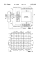
- FIG. 1 illustrates in block diagram form a flash EEPROM system utilizing the present invention
- FIG. 2 is a plan view of a first embodiment of a memory cell array of the present invention
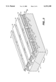
- FIG. 3 is an isometric view of the memory cell array of FIG. 2;
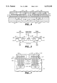
- FIG. 4 is a cross-sectional view of the memory cell array of FIGS. 2 and 3, taken at section I--I thereof,
- FIG. 5 is an electrical equivalent circuit of one of the memory cells of the array of FIGS. 2 and 3;
- FIG. 6 is an isometric view of a second embodiment of a memory cell array of present invention.
- FIG. 7 is a cross-sectional view of the memory cell array of FIG. 6, taken at section II--II thereof;
- FIG. 8 is a table giving example voltages of one way to operate either of the first or second embodiments of the present invention.
- FIG. 9 is a diagram showing an example of multiple states of operation of either of the first or second embodiments of the present invention.
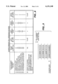
- FIG. 10 is a schematic diagram of a portion of a memory cell array according to the present invention.
- FIG. 1 An example memory system incorporating the various aspects of the present invention is generally illustrated in the block diagram of FIG. 1.
- a large number of individually addressable memory cells 11 are arranged in a regular array of rows and columns, although other physical arrangements of cells are certainly possible.
- Bit lines designated herein to extend along columns of the array 11 of cells, are electrically connected with a bit line decoder and driver circuit 13 through lines 15.
- Word lines which are designated in this description to extend along rows of the array 11 of cells, are electrically connected through lines 17 to a word line decoder and driver circuit 19.
- Steering gates which extend along columns of memory cells in the array 11, are electrically connected to a steering gate decoder and driver circuit 21 through lines 23.
- Each of the decoders 13, 19 and 21 receives memory cell addresses over a bus 25 from a memory controller 27.
- the decoder and driving circuits are also connected to the controller 27 over respective control and status signal lines 29, 31 and 33. Voltages applied to the steering gates and bit lines are coordinated through a bus 22 that interconnects the decoder and driver circuits 13 and 21.
- the controller 27 is connectable through lines 35 to a host device (not shown).
- the host may be a personal computer, notebook computer, digital camera, audio player, various other hand held electronic devices, and the like.
- the memory system of FIG. 1 will commonly be implemented in a card according to one of several existing physical and electrical standards, such as one from the PCMCIA, the CompactFlashTM Association, the MMCTM Association, and others.
- the lines 35 terminate in a connector on the card which interfaces with a complementary connector of the host device.
- the electrical interface of many cards follows the ATA standard, wherein the memory system appears to the host as if it was a magnetic disk drive. Other memory card interface standards also exist.
- memory systems of the type shown in FIG. 1 are permanently embedded in the host device.
- the decoder and driver circuits 13, 19 and 21 generate appropriate voltages in their respective lines of the array 11, as addressed over the bus 25, according to control signals in respective control and status lines 29, 31 and 33, to execute programming, reading and erasing functions. Any status signals, including voltage levels and other array parameters, are provided by the array 11 to the controller 27 over the same control and status lines 29, 31 and 33.
- a plurality of sense amplifiers within the circuit 13 receive current or voltage levels that are indicative of the states of addressed memory cells within the array 11, and provides the controller 27 with information about those states over lines 41 during a read operation.
- a large number of sense amplifiers are usually used in order to be able to read the states of a large number of memory cells in parallel.
- one row of cells is typically addressed at a time through the circuits 19 for accessing a number of cells in the addressed row that are selected by the circuits 13 and 21.
- all cells in each of many rows are typically addressed together as a block for simultaneous erasure.
- FIGS. 2--7 Two structural embodiments of the memory cell array 11 are shown in FIGS. 2--7, where the substrate and conductive elements are illustrated with little detail of dielectric layers that exist therebetween. This simplifies the Figures but it will be understood that appropriate oxide layers, those both grown and deposited, deposited silicon nitride layers, and other dielectrics commonly used are to be included between the conductive layers themselves and the conductive layers and the substrate.
- a usual silicon substrate 45 includes a planar top surface 47.
- Elongated diffusions 49, 51 and 53 are formed into the substrate 45 through the surface 47 by an initial ion implantation and subsequent diffusion, and serve as sources and drains of the memory cells formed between them.
- the diffusions are shown to be spaced apart in a first "x" direction, with lengths extending in a second "y” direction, these first and second directions being essentially orthogonal with each other.
- a large number of floating gates are included across the substrate surface 47 with suitable gate dielectric therebetween, in an array of rows and columns.
- floating gates 55-60 is adjacent to and parallel with another row of floating gates 62-67, for example, and a column of floating gates 69, 55, 62, 71 and 73 is adjacent to and parallel with a column of floating gates 75, 56, 63, 77 and 79.
- the floating gates are formed from a first layer of conductively doped polycrystalline silicon (“polysilicon”) that is deposited over the entire surface and then separated, by etching through a mask, into the individual floating gates.
- polysilicon conductively doped polycrystalline silicon
- the bit line decoder and driver circuit 13 (FIG. 1) is connected through lines 15 with all of the bit line source/drain diffusions of the array, including the diffusions 49, 51 and 53 of FIGS. 2-4.
- the sources and drains of columns of individual memory cells are connected to proper programming voltages for either reading or programming in response to addresses supplied over the bus 25 and control signals over the lines 19.
- FIGS. 2-4 uses one wider steering gate for every two columns of floating gates.
- Steering gates 81, 83 and 85 are elongated in the y-direction and have a width in the x-direction that extends across two adjacent columns of floating gates and a source/drain diffusion that is positioned in between them.
- the space between any two of the steering gates is at least as great as the space in the x-direction between adjacent columns of floating gates that are overlaid by the two steering gates, in order to allow a gate to be later formed at the substrate in this space.
- the steering gates are formed by etching a second layer of conductively doped polysilicon that is deposited over the entire surface over the first polysilicon layer and an appropriate inter-polysilicon layer dielectric.
- the steering gate decoder and driver circuit 21 (FIG. 1) connects though lines 23 to all the steering gates and is able to individually control their voltages in response to addresses provided on the bus 25, control signals in the lines 33, and data from the drivers and sense amplifiers 13.
- Word lines 91-95 of FIGS. 2-4 are elongated in the x-direction and extend over the steering gates with spaces between them in the y-direction that places each word line in alignment with a row of floating gates.
- the word lines are formed by etching a third layer of conductively doped polysilicon that is deposited over the entire surface on top of a dielectric that is first formed over the second polysilicon layer and regions exposed between the steering gates.
- the word lines allow selection of all the memory cells in its row for reading or writing.
- the select gate decoder and driver circuit 19 (FIG. 1) is connected with each word line in order to individually select one row of the cell array. Individual cells within a selected row are then enabled for reading or writing by the bit line and steering gate decoder and driver circuits 13 and 21.
- the gates in the foregoing structure are preferably made of doped polysilicon material, other suitable electrically conductive materials may be used in place of one or more of the three polysilicon layers described.
- the third layer for example, from which the word lines and select gates are formed, may be a polycide material, which is polysilicon with a conductive refractive metal silicide on its top, such as tungsten, in order to increase its conductivity.
- Polycides are generally not used in place of either the first or second polysilicon layers because the quality of oxide grown from a polycide is usually not satisfactory.
- metal conductor layers are included in separate layers, with connections made to respective metal lines through any intermediate layers at periodical intervals along the lengths of the polysilicon elements and diffusions. Since all of the diffusions and polysilicon elements of the embodiment of FIGS. 2-4 need to be separately driven, there is a one-to-one correspondence between the number of these metal lines and the number of diffusions and polysilicon elements.
- One advantage of reducing the number of steering gates by one-half, a result of the present invention, is that the number of corresponding metal lines necessary to be connected to the steering gates is also reduced by one-half This is significant because present processing techniques are generally not able to form the metal lines with the same small pitch as diffusions and polysilicon elements.
- the reduction in number of metal conductors in any integrated circuit has the potential of reducing its size and complexity, to improve its operation, and increase the manufacturing yield.
- FIG. 5 An electrical equivalent circuit is given in FIG. 5, where equivalent elements are identified by the same reference numbers as in FIGS. 2-4 but with a prime (') added.
- the illustrated cell shares the source and drain diffusions with its neighboring cells. Conduction through the cell's channel in the substrate between the adjacent diffusions 49 and 51 is controlled by different gate elements in three different regions. A first region to the left (L1-left) has the floating gate 56 immediately above it and the steering gate 81 capacitively coupled with it. A second region to the right (L1-right) is controlled in a similar manner by the floating gate 57 and the steering gate 83.
- a third region L2, in between the first two, is controlled by a select gate 99 that is part of the word line 92 formed from the third polysilicon layer with a gate dielectric layer between it and the substrate surface 47.
- a select gate 99 that is part of the word line 92 formed from the third polysilicon layer with a gate dielectric layer between it and the substrate surface 47.
- the level of conduction of electrons through the cell's channel between the diffusions 49 and 51 is thus affected by the electric fields imparted by these different gate elements to their respective channel regions by the voltages placed on the gates.
- the voltage on a floating gate is dependent upon the level of net electrical charge it carries plus all displacement charge that is capacitively coupled from other gates and nodes.
- the level of conduction that is permitted through the channel portion under a floating gate is controlled by the voltage on that floating gate.
- the voltage on the select gate 99 simply turns the channel on and off to any conduction in order to select individual cells for connection with their source/drain regions.
- An individual cell can be considered as a series connection of three transistors, one for each of the three different regions of the channel, as illustrated in the equivalent circuit of FIG. 5.
- the gate elements 56, 57 and 99 are the only gates that control conduction through the memory cell shown in FIG. 4, but the voltages on gates 56 and 57 are affected by the voltages on other gate, source and drain elements through capacitive coupling with them.
- Another advantage of spanning two floating gate columns with a single steering gate is that the level of capacitive coupling between the floating and steering gates is increased while the coupling between the floating gate and the word line is decreased. Since the steering gate 81, for example, extends across an edge 101 of the floating gate 56 in the x-direction, that edge is shielded from coupling with the word line 92. Instead of the word line 92 extending downward between adjacent floating gates 55 and 56, as is most likely the case when the steering gate is no wider in the x-direction than the floating gate which it overlies, coupling of the word line with the floating gate edge 101 is eliminated by the steering gate extending across to the adjacent floating gate 55 and thereby providing a shield between the word line 92 and the edge 101 of the floating gate.
- Coupling between the floating gate 56 and the steering gate 81 is then optionally but desirably further increased by extending a portion 109 the steering gate 81 downward adjacent the floating gate edge 101. Coupling between the floating gate 56 and the word line 92 is then effectively reduced to the small area along an opposite floating gate edge 103. This significant reduction of the capacitive coupling between the floating gate and word line is very beneficial. By increasing the amount of coupling between steering and floating gates relative to the coupling of the floating gate with the substrate and the word line, less voltage need be applied to the steering gate to bring about a desired result in the memory cell's channel portion under that floating gate.
- a benefit that results from a reduced steering gate voltage is a reduced stress on the dielectric layer between the steering gate and the substrate, and on the dielectric layer between the steering gate and the word line, since the substrate and word line are typically operated at lower voltages than the steering gate during reading and programming operations.
- One of the two floating gates of a single memory cell is selected for programming or reading by placing a voltage on the steering gate above the other floating gate of the cell that is sufficient to cause the channel region under the other floating gate become adequately conductive no matter what charge (which is related to its state) is carried by that other (non-selected) floating gate.
- that cell's select transistor When that cell's select transistor is turned on by a sufficient voltage applied to its word line, it is only the selected floating gate that responds to reading or programming operations directed to the cell.
- current through the cell between its source and drain is then dependent upon the charge carried by the selected floating gate without regard to the charge on the other floating gate.
- the voltage placed on the steering gate over the non-selected floating gate to render the channel portion under the non-selected floating gate conductive is also coupled to an adjacent floating gate of an adjacent cell through the same steering gate, impact on the adjacent cell is avoided by placing proper voltage conditions on the other elements of the adjacent cell.
- the memory cell floating gates of the embodiment of FIGS. 2-4 are preferably programmed by placing voltages on its bit lines (source and drain diffusions) and its two steering gates that cause electrons to obtain enough energy in the substrate channel region to be injected across the gate dielectric onto the selected floating gate.
- a preferred technique for this is "source side injection,” described in the afore referenced U.S. Pat. Nos. 5,313,421 and 5,712,180.
- the memory cells of the embodiment of FIGS. 2-4 may be designed and operated so that electrons are removed from the selected floating gates to either the channel or the select gate of the word line.
- the dielectric between the floating gate edge 103 and the select gate 99 is preferably a thin layer of oxide that has been grown on the floating gate edge and through which electrons tunnel when appropriate voltages are placed on the various elements of the cell. The same is provided between the floating gate edge 105 and the select gate 99.
- the dielectric between the edges of the floating gates and the select gate may be made thicker and of a type that reduces the coupling between them.
- the dashed lines of FIG. 5 illustrate the coupling that exists when erasing to the select gate.
- the embodiment of FIGS. 2-4 is modified somewhat.
- the dielectric between the select gate 99 and the adjacent floating gate edges 103 and 105 is made to be thicker to prevent erasing of the floating gates to the select gate.
- the thickness of the gate dielectric between an underside of the floating gates and the substrate surface 47 is made thinner, such as about 100 Angstroms, to facilitate electrons tunneling through it.
- the cells to be simultaneously erased as a block are grouped together and isolated on the substrate from other blocks.
- n-well is formed in a p-substrate, and a p-well carrying the block of cells is positioned within the n-well that isolates the block from others.
- An appropriate erase voltage is then applied to the p-wells of the blocks to be erased, while other blocks are not affected.
- Another advantage of using the wider steering gates of the present invention, particularly when the floating gates are erased to the select gates of the word lines carrying a high voltage, is that the steering gates separate the word lines from the diffusions, thereby eliminating possible breakdown of a dielectric that exists between the word line and the diffusion in prior dual gate structures.
- the word line is typically raised to a level in excess of 10 volts and sometimes to 20 volts or more during erase, while other voltages applied to the cell are usually 5 volts or less.
- the voltage gradient across the select gate dielectric can be reduced by making it thicker or selected to have a dielectric constant that is higher than normally used but that can adversely affect operation of the select transistor.
- the cell may be operated with a lower voltage difference between the select gate and the substrate during erase.
- the wider steering gates also help make the reduced select transistor gate dielectric voltage possible because they increase the proportion of the floating gates' coupling with the steering gates vs. that with the substrate channel and word line, so an increase of the substrate channel voltage, which results from the positive source and drain potentials during erase, is not translated into a very significant increase of the floating gate voltage.
- the steering gates when maintained at ground potential, for example, are better able to hold their floating gates near ground because of this increased capacitive coupling. Since there is some degree of coupling between the substrate channel and the floating gates, and because increasing the voltages on the diffusions places added strains on other dielectrics and junctions, there is a limit of how high this voltage can be made.
- the word line is raised to about 20 volts and the bit line diffusions to about 5 volts during erase.
- the result of reducing the voltage differential between the select gate and the substrate channel is to reduce the degree to which some characteristic of the select gate dielectric must be altered (such as its thickness or composition) from what is optimal for operation of the select transistor.
- the amount of area taken by each cell can be further reduced by taking advantage of the feature of adjacent floating gate columns sharing a common steering gate.
- the first embodiment of FIGS. 2-4 wherein the floating gates are arranged in a plane parallel to the planar surface of the substrate, can be modified to place a majority of the floating gates along opposing sides of a trench with the common steering gate positioned between them.
- An example of such a modified structure is illustrated in FIGS. 6 and 7.
- the cells are horizontally compacted in the x-direction by extending the floating gates down into trenches in the substrate.
- This configuration also allows the floating gates to be made larger in effective length without increasing the horizontal (x-direction) extent of the dual floating gate memory cell, since the floating gates are extended downward into the trenches, thus increasing the density of the floating gates and consequently of the data stored in an array of a given area for floating gates of a given length.
- trenches 115-118 are formed in a planar top surface 121 of a semiconductive substrate 119.
- the trenches are elongated in the y-direction across the substrate, are parallel with each other and are spaced apart in the x-direction. It is preferable, in order to minimize the size of each cell, that the side walls of the trenches be perpendicular with the substrate surface 121 but this makes it difficult to form by present processing technology. Therefore, the trench walls are slightly tilted in the x-direction away from a center of the trench by an angle ⁇ .
- the angle ⁇ is made as small as possible, less than about 15 degrees, as permitted by the processing technology that forms the floating gates.
- the trenches are formed as an initial step by choosing an etching technology and materials to provide the trenches with the desired side wall angle ⁇ .
- source and drain diffusions 131-134 are implanted in the bottom of the trenches and they subsequently diffuse outwardly and slightly up along the trench side walls.
- a layer of floating gate oxide dielectric is formed over the structure, particularly along the side walls of the trenches.
- Floating gates 123-130 are then formed from a first doped polysilicon layer that is etched away through a mask to leave the floating gates isolated from one another. It is this etching step, which, for accurate dimensional control, is highly anisotropic, that is facilitated by the trench sidewalls having a slight angle ⁇ from the vertical. It is then easier to remove all of the first polysilicon layer from the trench walls and bottom in between the areas of polysilicon that are desired to remain as the floating gates.
- each trench is made to have a length in the y-direction that matches the dimension of the floating gate in that direction.
- Opposing end walls (not shown) in the y-direction are preferably also sloped in order to make it easier to remove some of the first polysilicon layer from those end walls.
- a single mask can be used to separate the first polysilicon layer into two floating gates in each trench and to subsequently implant the source and drain regions along lines extending through the trenches and between them.
- steering gates 137-140 are formed by depositing a second layer of polysilicon to fill the spaces remaining in the trenches between the dielectric layers covering the floating gates. This also covers the top of the first polysilicon structure with the second polysilicon layer, which is then etched though a mask to form separate steering gates that are elongated in the y-direction. The first polysilicon layer strips are then etched, self-aligned with edges of the second polysilicon layer steering gates, to form isolated floating gate islands. As in the embodiment of FIGS. 2-4, each steering gate is capacitively coupled with adjacent floating gates of adjacent cells and extends across a diffusion that exists between the cells.
- Word lines 143 and 145 are formed from a third polysilicon layer, with select gates extending downward as part of each word line polysilicon into each dual floating gate cell along its row.
- Select gates 146-148 are illustrated in FIGS. 6 and 7 as elements of three respective contiguous cells along a row.
- a select transistor is formed in the channel region L2 on the surface 121 of the substrate 119 under the select gate 147.
- a left L1 channel region extends on one side of the region L2 to the diffusion 132, and a right L1 channel region extends on the other side of the region L2 to the diffusion 133.
- each of the L1 channel regions includes a portion on the surface 121 and most of a sidewall of one of the trenches 116 and 117.
- the same considerations of erasing the floating gates of a cell to either the substrate 119 or to the select gate 147 that were discussed with respect to the first embodiment apply to this embodiment as well.
- the channel is advantageously raised in voltage when the high erase voltage is applied to the select gate in order to reduce stress on the select transistor dielectric between the select gate 147 and the substrate surface 121.
- This second cell array embodiment also has the same advantages discussed above with respect to the first embodiment, except that the width of the steering gates will usually be a minimum feature size that the current processing techniques can implement.
- the advantages of facilitating future scaling of the circuit and making it easier to electrically contact the steering gates, as discussed above for the first embodiment, are thus reduced in the second embodiment.
- the steering gates in the second embodiment do have an increased cross-section, with a resulting increased conductivity that reduces the frequency of the contacts that must be provided between the steering gates and metal conductors of another layer. And there are one-half the number of steering gates, thus requiring only one-half the number of metal conductors connected to them.
- the coupling between a floating gate and its steering gate is increased relative to the coupling between the floating gate and its word line and substrate, as in the first embodiment.
- the word lines and their select gates in the second embodiment are even further isolated from the diffusions than in the first embodiment since the diffusions are removed to the bottom of the trenches, in addition to interposing the select gates therebetween.
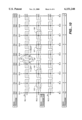
- Example operating voltages to program, read and erase the memory cells of the array of the first embodiment are given in a table of FIG. 8. Except where noted herein, the same operating voltages are applied to the cells of the array of the second embodiment.
- Lines (1)-(7) pertain to the operation of the type of cells that are erased to the select gates (word lines), while line (8) shows a modification for operating the type of cells that are erased to the substrate.
- the substrate portion in which the cells are formed contains p-type doping and the bit line diffusions are of n-type. The substrate is held at ground potential throughout these operations.
- the second line (2) of the FIG. 8 table gives an example set of voltages for erasing the type of cells designed to be erased to the word line's select gate.
- a high erase voltage V E in a range of 10-25 volts with 20 volts preferred, is applied by driver circuits 19 to all the word lines whose memory cell floating gates are to be erased.
- This is usually at least one defined block of cells including all cells in a large number of contiguous rows, in order to amortize the time of an erase operation over a very large number of memory cells.
- fewer cells may be simultaneously erased.
- the erase block can, alternatively, even be limited to a single row of cells.
- the steering gates of the cells along the one or more selected rows are set to a low voltage by the driving circuit 21, such as zero volts, in order to maintain, by the high degree of capacitive coupling between the steering and floating gates, the voltage of the floating gates at a low level.
- the resulting potential difference between the floating gates and their respective select gates (word lines) causes electron tunneling through the intermediate dielectric.
- the bit line diffusions of all the cells being simultaneously erased are raised above zero by one or more volts by the driving circuit 13.
- this increased voltage appearing in the floating gate channel regions from their adjacent source or drain also causes the voltage of the floating gate to be increased somewhat, thus diminishing the voltage difference between the floating and select gates, but this is acceptable in light of the advantages to the construction and operation of the select transistor that the higher substrate channel voltage brings about.
- bit line diffusions 5 volts is applied to the bit line diffusions, which, as can be seen from the table of FIG. 8, is the highest voltage that is ever applied to the bit lines, during any operation. Consequently, this is the maximum voltage that the junctions formed by the diffusions with the substrate are designed to safely withstand, the substrate being held at ground potential during all operations. This limited required maximum voltage facilitates both the design of this junction and its scalability.
- Lines (3) and (4) give example voltages for reading the state of the two floating gates of a memory cell, line (3) for the left floating gate and line (4) for the right floating gate.
- the cell is enabled by the select gate being raised to a voltage V SR sufficient to turn on the cell's select transistor to enable current flow through the channel.
- V SR 2 volts for a select transistor floating gate to be read is held at zero volts, for optimal read precision, especially when used in conjunction with a multi-level storage operation, by minimizing additional coupling from the bit line to the floating gate being read.
- the other bit line is given a level equal to an optimum sensing bias of the sense amplifier within the circuit 13 that is used in the reading process, such as one volt.
- the higher voltage on the bit line adjacent the floating gate not being read also assists in over driving that floating gate, further limiting its impact on sensing the charge level of the targeted floating gate.
- FIG. 9 illustrates operating with a floating gate voltage window divided into four states, thus storing 2 bits per floating gate and 4 bits of information per memory cell. Operation with even more states is desirable to further increase the density of data that can be stored in a given memory cell array. For example, 16 state operation results in storing 4 bits of data per floating gate and 8 bits of information per memory cell.
- the steering gate over the floating gate being read has a voltage V M applied to it and the steering gate over the other floating gate of the cell is raised to V BR , as shown in lines (3) and (4) of the table of FIG. 8.
- the voltage V BR is made to be high enough, an example being 8 volts, to render the cell's channel portion under the non-selected floating gate sufficiently conductive, no matter what the programmed state of the non-selected floating gate.
- the voltage V M is scanned or stepped between two voltages during the reading step, and its value when the cell current passes through a defined threshold is detected by the sense amplifiers within the circuit 13. This detected value of V M is indicative of the state (FIG. 9) in which the selected floating gate has been programmed.
- Example voltages for programming one floating gate of a dual floating gate cell are given in lines (5) and (6) of the table of FIG. 8.
- the select gate is raised sufficiently to turn on the cell's select transistor.
- the voltage V SP may be different from the voltage V SR used during reading in order to optimize the source side injection programming speed.
- the bit line diffusion on the same side of the cell as the floating gate selected to be programmed is raised to a maximum bit line voltage, 5 volts in this example, during the programming operation. This voltage is made high enough to enable a high enough field to be built up across the gap between the floating and select gate channels to obtain source side hot electron programming.
- the bit line diffusion on the same side of the cell as the non-selected floating gate is held at zero volts during programming.
- the steering gate over the non-selected floating gate is raised to a voltage V BP that is sufficient to render sufficiently conductive the channel region under the non-selected floating gate in order to pose no interference to programming of the target floating gate, no matter what floating gate voltage exists on the non-selected floating gate, within a programming window range of floating gate voltages.
- the voltage V BP is made higher than the voltage V BR used during reading in order to turn on that portion of the cell channel harder in light of higher voltages being applied to other elements of the cell.
- a voltage V P is applied to the steering gate over the selected floating gate with a level that drives the selected floating gate to a voltage that assists in creating the desired field conditions in the channel below it for hot electron programming. For example, the voltage V P within the range of 5-12 volts is suitable.
- This voltage may vary during the programming operation.
- the appropriate set of programming voltages is first applied to a erased cell, followed by the appropriate set of reading voltages, and, if the reading step does not indicate that the selected floating gate has been programmed to the desired voltage state, which may be the programming state for binary storage or one of the variable storage states for multi-level storage, programming voltages are again applied which may in part be different from the earlier set.
- a last line (7) of the table of FIG. 8 shows voltages that are applied to those cells within a row selected for programming that are themselves not to be programmed. That is, the number of cells programmed at the same time within one row of a segmented portion of an array are spaced alternately along the row with other cells in between them that are not being programmed. It is these other cells not being programmed that receive the voltages of line (7) of the table of FIG. 8.
- the opposing bit line diffusions are maintained at the same voltage in order to prevent any current from flowing, in the channel, such as both zero or both 5 volts.
- the "x" indicates that the voltages on the steering gates of these cells do not matter, in either case.
- erase voltage conditions of line (8) are applied instead of those of line (2).
- Both the p-well containing a block of cells to be erased and its surrounding n-well are raised to the erase voltage V E , within an example range of 10-25 volts with 20 volts preferred. (During reading and programming such cells, their wells are held at ground potential.)
- a positive voltage V SE is preferably applied to the select gates during erase in order to reduce the voltage applied across the select gate dielectric, since an excessive voltage differential between the substrate and select gate can damage the dielectric material or cause it to be made thicker than otherwise desirable for operation of the cells.
- the voltages of the table of FIG. 8 are shown applied to a portion of an array of memory cells, represented schematically, for simultaneously programming or reading the states of multiple floating gates along a selected row.
- Bit lines are labeled in FIG. 10 as BL1, BL2, etc.
- steering gate connections are identified as SG1, SG2, etc.
- Word lines are denoted as WL1, WL2, etc.
- a typical cell 151 is labeled with the same reference numbers of the cell illustrated in FIGS. 4 and 5 but with a double prime (") added. An array of 3 rows and 8 columns of such cells are shown. Using the voltages of the table of FIG.
- floating gates within cell halves 153, 155, 157 and 159 are either being read or programmed at the same time, depending upon whether the read or program voltages are being applied to the word lines, bit lines and steering gates. That is one floating gate from every other cell along the selected row. The remaining intermediate cells of the selected row have equal voltages applied to their bit lines, so no current flows through the channels of those cells. An entire row, or designated portion of a row, of cells may be read or programmed by a sequence of four simultaneous such operations. Alternatively, in order to reduce the power required for each read or to space the sense amplifiers further apart along the columns, one floating gate from every fourth cell along the selected row may be read, while the voltages of the bit lines of cells intermediate of those being read are made equal.
Landscapes
- Engineering & Computer Science (AREA)
- Computer Hardware Design (AREA)
- Microelectronics & Electronic Packaging (AREA)
- Non-Volatile Memory (AREA)
Abstract
Description
Claims (31)
Priority Applications (3)
| Application Number | Priority Date | Filing Date | Title |
|---|---|---|---|
| US09/343,328 US6151248A (en) | 1999-06-30 | 1999-06-30 | Dual floating gate EEPROM cell array with steering gates shared by adjacent cells |
| US09/634,694 US6266278B1 (en) | 1999-06-30 | 2000-08-08 | Dual floating gate EEPROM cell array with steering gates shared adjacent cells |
| US09/904,945 US6344993B1 (en) | 1999-06-30 | 2001-07-13 | Dual floating gate EEPROM cell array with steering gates shared by adjacent cells |
Applications Claiming Priority (1)
| Application Number | Priority Date | Filing Date | Title |
|---|---|---|---|
| US09/343,328 US6151248A (en) | 1999-06-30 | 1999-06-30 | Dual floating gate EEPROM cell array with steering gates shared by adjacent cells |
Related Child Applications (1)
| Application Number | Title | Priority Date | Filing Date |
|---|---|---|---|
| US09/634,694 Continuation US6266278B1 (en) | 1999-06-30 | 2000-08-08 | Dual floating gate EEPROM cell array with steering gates shared adjacent cells |
Publications (1)
| Publication Number | Publication Date |
|---|---|
| US6151248A true US6151248A (en) | 2000-11-21 |
Family
ID=23345655
Family Applications (3)
| Application Number | Title | Priority Date | Filing Date |
|---|---|---|---|
| US09/343,328 Expired - Lifetime US6151248A (en) | 1999-06-30 | 1999-06-30 | Dual floating gate EEPROM cell array with steering gates shared by adjacent cells |
| US09/634,694 Expired - Lifetime US6266278B1 (en) | 1999-06-30 | 2000-08-08 | Dual floating gate EEPROM cell array with steering gates shared adjacent cells |
| US09/904,945 Expired - Fee Related US6344993B1 (en) | 1999-06-30 | 2001-07-13 | Dual floating gate EEPROM cell array with steering gates shared by adjacent cells |
Family Applications After (2)
| Application Number | Title | Priority Date | Filing Date |
|---|---|---|---|
| US09/634,694 Expired - Lifetime US6266278B1 (en) | 1999-06-30 | 2000-08-08 | Dual floating gate EEPROM cell array with steering gates shared adjacent cells |
| US09/904,945 Expired - Fee Related US6344993B1 (en) | 1999-06-30 | 2001-07-13 | Dual floating gate EEPROM cell array with steering gates shared by adjacent cells |
Country Status (1)
| Country | Link |
|---|---|
| US (3) | US6151248A (en) |
Cited By (175)
| Publication number | Priority date | Publication date | Assignee | Title |
|---|---|---|---|---|
| US6266278B1 (en) * | 1999-06-30 | 2001-07-24 | Sandisk Corporation | Dual floating gate EEPROM cell array with steering gates shared adjacent cells |
| US6304484B1 (en) * | 1999-12-27 | 2001-10-16 | Hyundai Electronics Industries Co., Ltd. | Multi-bit flash memory cell and programming method using the same |
| US6324097B1 (en) * | 1999-08-26 | 2001-11-27 | Mosel Vitelic Inc. | Single poly non-volatile memory structure and its fabricating method |
| US6420231B1 (en) | 1999-06-30 | 2002-07-16 | Sandisk Corporation | Processing techniques for making a dual floating gate EEPROM cell array |
| US6462375B1 (en) * | 2002-04-01 | 2002-10-08 | Silicon Based Technology Corp. | Scalable dual-bit flash memory cell and its contactless flash memory array |
| US6469342B1 (en) * | 2001-10-29 | 2002-10-22 | Macronix International Co., Ltd. | Silicon nitride read only memory that prevents antenna effect |
| US6479858B2 (en) * | 1997-07-09 | 2002-11-12 | Advanced Micro Devices, Inc. | Method and apparatus for a semiconductor device with adjustable threshold voltage |
| WO2002097820A2 (en) * | 2001-05-31 | 2002-12-05 | Sandisk Corporation | Pair wise programming method for dual cell eeprom |
| US6512263B1 (en) | 2000-09-22 | 2003-01-28 | Sandisk Corporation | Non-volatile memory cell array having discontinuous source and drain diffusions contacted by continuous bit line conductors and methods of forming |
| US6522580B2 (en) * | 2001-06-27 | 2003-02-18 | Sandisk Corporation | Operating techniques for reducing effects of coupling between storage elements of a non-volatile memory operated in multiple data states |
| US20030039146A1 (en) * | 2001-08-25 | 2003-02-27 | Choi Woong Lim | Non-volatile semiconductor memory and method of operating the same |
| US6532172B2 (en) | 2001-05-31 | 2003-03-11 | Sandisk Corporation | Steering gate and bit line segmentation in non-volatile memories |
| US6542407B1 (en) | 2002-01-18 | 2003-04-01 | Sandisk Corporation | Techniques of recovering data from memory cells affected by field coupling with adjacent memory cells |
| US6563728B2 (en) * | 2000-06-12 | 2003-05-13 | Sony Corporation | Semiconductor memory device and method for operation thereof |
| US20030109093A1 (en) * | 2001-10-31 | 2003-06-12 | Eliyahou Harari | Multi-state non-volatile integrated circuit memory systems that employ dielectric storage elements |
| US20030161185A1 (en) * | 2002-02-28 | 2003-08-28 | Sandisk Corporation | Method and system for efficiently reading and programming of dual cell memory elements |
| WO2003073290A1 (en) | 2002-02-22 | 2003-09-04 | Sandisk Corporation | Pipelined parallel programming operation in a non-volatile memory system |
| US6620683B1 (en) | 2001-12-04 | 2003-09-16 | Taiwan Semiconductor Manufacturing Company | Twin-bit memory cell having shared word lines and shared bit-line contacts for electrically erasable and programmable read-only memory (EEPROM) and method of manufacturing the same |
| US6627927B2 (en) * | 2002-01-30 | 2003-09-30 | Ching-Yuan Wu | Dual-bit flash memory cells for forming high-density memory arrays |
| US6639309B2 (en) | 2002-03-28 | 2003-10-28 | Sandisk Corporation | Memory package with a controller on one side of a printed circuit board and memory on another side of the circuit board |
| US6646916B2 (en) * | 2001-04-13 | 2003-11-11 | Seiko Epson Corporation | Non-volatile semiconductor memory device |
| US6645813B1 (en) | 2002-01-16 | 2003-11-11 | Taiwan Semiconductor Manufacturing Company | Flash EEPROM with function bit by bit erasing |
| US20030209751A1 (en) * | 2001-05-18 | 2003-11-13 | Sandisk Corporation | Floating gate memory cells utilizing substrate trenches to scale down their size |
| US6650591B2 (en) * | 2001-05-31 | 2003-11-18 | Seiko Epson Corporation | Nonvolatile semiconductor memory device |
| US20040000688A1 (en) * | 2001-05-18 | 2004-01-01 | Sandisk Corporation | Non-volatile memory cells utilizing substrate trenches |
| US6684289B1 (en) | 2000-11-22 | 2004-01-27 | Sandisk Corporation | Techniques for operating non-volatile memory systems with data sectors having different sizes than the sizes of the pages and/or blocks of the memory |
| US20040056299A1 (en) * | 2002-09-19 | 2004-03-25 | Yi Ding | Nonvolatile memory cell with a floating gate at least partially located in a trench in a semiconductor substrate |
| US20040070021A1 (en) * | 2002-10-09 | 2004-04-15 | Yuan Jack H. | Flash memory array with increased coupling between floating and control gates |
| US20040095797A1 (en) * | 2001-08-08 | 2004-05-20 | Sandisk Corporation | Scalable self-aligned dual floating gate memory cell array and methods of forming the array |
| US6747896B2 (en) | 2002-05-06 | 2004-06-08 | Multi Level Memory Technology | Bi-directional floating gate nonvolatile memory |
| US6781877B2 (en) | 2002-09-06 | 2004-08-24 | Sandisk Corporation | Techniques for reducing effects of coupling between storage elements of adjacent rows of memory cells |
| US20040179404A1 (en) * | 2001-12-18 | 2004-09-16 | Quader Khandker N. | Method and system for programming and inhibiting multi-level, non-volatile memory cells |
| US6798012B1 (en) * | 1999-12-10 | 2004-09-28 | Yueh Yale Ma | Dual-bit double-polysilicon source-side injection flash EEPROM cell |
| US20040190347A1 (en) * | 2001-09-17 | 2004-09-30 | Raul-Adrian Cernea | Dynamic column block selection |
| US20040196694A1 (en) * | 2003-04-07 | 2004-10-07 | Bomy Chen | Bi-directional read/program non-volatile floating gate memory cell with independent controllable control gates, and array thereof, and method of formation |
| US20040195615A1 (en) * | 2003-04-07 | 2004-10-07 | Bomy Chen | Bi-directional read/program non-volatile floating gate memory cell and array thereof, and method of formation |
| US20040214393A1 (en) * | 2003-04-23 | 2004-10-28 | Geeng-Chuan Chern | Non-volatile floating gate memory cell with floating gates formed as spacers, and an array thereof, and a method of manufacturing |
| US6818512B1 (en) * | 2002-01-04 | 2004-11-16 | Taiwan Semiconductor Manufacturing Company | Split-gate flash with source/drain multi-sharing |
| US20040232496A1 (en) * | 2003-05-21 | 2004-11-25 | Jian Chen | Use of voids between elements in semiconductor structures for isolation |
| US20040257877A1 (en) * | 2003-06-20 | 2004-12-23 | Raul-Adrian Cernea | Source controlled operation of non-volatile memories |
| US20040259291A1 (en) * | 2003-06-23 | 2004-12-23 | Sandisk Corporation | Method for efficiently producing removable peripheral cards |
| US20040262668A1 (en) * | 2003-06-24 | 2004-12-30 | Taiwan Semicondutor Manufacturing Co. | Novel dual bit split gate flash memory |
| US20050003616A1 (en) * | 2003-06-20 | 2005-01-06 | Jeffrey Lutze | Self aligned non-volatile memory cell and process for fabrication |
| US20050007801A1 (en) * | 2001-09-17 | 2005-01-13 | Ron Barzilai | Multi-purpose non-volatile memory card |
| US20050014298A1 (en) * | 2003-07-17 | 2005-01-20 | Takiar Hem P. | Memory card with raised portion |
| US20050011671A1 (en) * | 2003-07-17 | 2005-01-20 | Takiar Hem P. | Memory card with and without enclosure |
| US20050012137A1 (en) * | 2003-07-18 | 2005-01-20 | Amitay Levi | Nonvolatile memory cell having floating gate, control gate and separate erase gate, an array of such memory cells, and method of manufacturing |
| US20050037573A1 (en) * | 2003-08-12 | 2005-02-17 | Kwan-Ju Koh | Flash memories and methods of fabricating the same |
| US20050056887A1 (en) * | 2003-09-17 | 2005-03-17 | Micron Technologies, Inc. | DRAM access transistor and method of formation |
| US20050072999A1 (en) * | 2003-10-06 | 2005-04-07 | George Matamis | Bitline direction shielding to avoid cross coupling between adjacent cells for NAND flash memory |
| KR100485502B1 (en) * | 2002-09-19 | 2005-04-27 | 동부아남반도체 주식회사 | Nonvolatile memory device and method for manufacturing thereof |
| US6888758B1 (en) | 2004-01-21 | 2005-05-03 | Sandisk Corporation | Programming non-volatile memory |
| US20050099849A1 (en) * | 2003-11-07 | 2005-05-12 | Lutze Jeffrey W. | Flash memory programming using gate induced junction leakage current |
| US20050102466A1 (en) * | 2003-01-28 | 2005-05-12 | Jian Chen | Non-volatile semiconductor memory with large erase blocks storing cycle counts |
| US6894930B2 (en) | 2002-06-19 | 2005-05-17 | Sandisk Corporation | Deep wordline trench to shield cross coupling between adjacent cells for scaled NAND |
| US20050104116A1 (en) * | 2003-11-13 | 2005-05-19 | Bomy Chen | Stacked gate memory cell with erase to gate, array, and method of manufacturing |
| US6897522B2 (en) | 2001-10-31 | 2005-05-24 | Sandisk Corporation | Multi-state non-volatile integrated circuit memory systems that employ dielectric storage elements |
| US20050141387A1 (en) * | 2003-12-31 | 2005-06-30 | Raul-Adrian Cernea | Flexible and area efficient column redundancy for non-volatile memories |
| US6914820B1 (en) | 2002-05-06 | 2005-07-05 | Multi Level Memory Technology | Erasing storage nodes in a bi-directional nonvolatile memory cell |
| US20050157549A1 (en) * | 2004-01-21 | 2005-07-21 | Nima Mokhlesi | Non-volatile memory cell using high-k material and inter-gate programming |
| US20050162924A1 (en) * | 2004-01-27 | 2005-07-28 | Guterman Daniel C. | Variable current sinking for coarse/fine programming of non-volatile memory |
| US20050162923A1 (en) * | 2004-01-27 | 2005-07-28 | Guterman Daniel C. | Charge packet metering for coarse/fine programming of non-volatile memory |
| US20050162916A1 (en) * | 2004-01-27 | 2005-07-28 | Guterman Daniel C. | Efficient verification for coarse/fine programming of non-volatile memory |
| US20050162927A1 (en) * | 2002-06-19 | 2005-07-28 | Henry Chien | Deep wordline trench to shield cross coupling between adjacent cells for scaled NAND |
| US20050195635A1 (en) * | 2004-03-08 | 2005-09-08 | Conley Kevin M. | Flash controller cache architecture |
| US20050199939A1 (en) * | 2004-03-12 | 2005-09-15 | Lutze Jeffrey W. | Self aligned non-volatile memory cells and processes for fabrication |
| US20050218444A1 (en) * | 2001-04-25 | 2005-10-06 | Seong-Gyun Kim | Non-volatile memory device |
| US20050237777A1 (en) * | 2004-04-22 | 2005-10-27 | Tsung-Min Hsieh | Nonvolatile memory device and method for fabricating the same |
| US20050239245A1 (en) * | 2001-12-10 | 2005-10-27 | Sharp Kabushiki Kaisha | Nonvolatile semiconductor memory and method of operating the same |
| US20050248988A1 (en) * | 2004-05-05 | 2005-11-10 | Guterman Daniel C | Boosting to control programming of non-volatile memory |
| US20060008983A1 (en) * | 2004-07-06 | 2006-01-12 | Macronix International Co., Ltd. | Method for manufacturing a multiple-gate charge trapping non-volatile memory |
| US20060007741A1 (en) * | 2004-07-06 | 2006-01-12 | Macronix International Co., Ltd. | Charge trapping non-volatile memory with two trapping locations per gate, and method for operating same |
| US20060007732A1 (en) * | 2004-07-06 | 2006-01-12 | Macronix International Co., Ltd. | Charge trapping non-volatile memory and method for operating same |
| US20060007735A1 (en) * | 2004-07-06 | 2006-01-12 | Macronix International Co., Ltd | Memory array including multiple-gate charge trapping non-volatile cells |
| US20060007742A1 (en) * | 2004-07-06 | 2006-01-12 | Macronix International Co., Ltd. | Charge trapping non-volatile memory and method for gate-by-gate erase for same |
| US20060039198A1 (en) * | 2004-05-05 | 2006-02-23 | Guterman Daniel C | Bitline governed approach for coarse/fine programming |
| US20060104120A1 (en) * | 2004-11-16 | 2006-05-18 | Hemink Gerrit J | High speed programming system with reduced over programming |
| US20060108648A1 (en) * | 2004-11-23 | 2006-05-25 | Yuan Jack H | Memory with self-aligned trenches for narrow gap isolation regions |
| US20060120165A1 (en) * | 2004-11-16 | 2006-06-08 | Hemink Gerrit J | Faster programming of higher level states in multi-level cell flash memory |
| US20060134864A1 (en) * | 2004-12-22 | 2006-06-22 | Masaaki Higashitani | Multi-thickness dielectric for semiconductor memory |
| EP1688959A1 (en) * | 2005-02-04 | 2006-08-09 | STMicroelectronics S.r.l. | Method for programming a memory device suitable to minimize the lateral coupling effects between memory cells |
| US20060261399A1 (en) * | 2005-05-20 | 2006-11-23 | Yuniarto Widjaja | Split gate NAND flash memory structure and array, method of programming, erasing and reading thereof, and method of manufacturing |
| JP2006332640A (en) * | 2005-05-20 | 2006-12-07 | Silicon Storage Technology Inc | Bidirectional split gate nand flash memory structure, array, programming method of the same, erasing method, readout method and manufacturing method |
| US7158420B2 (en) | 2005-04-29 | 2007-01-02 | Macronix International Co., Ltd. | Inversion bit line, charge trapping non-volatile memory and method of operating same |
| US20070059945A1 (en) * | 2005-09-12 | 2007-03-15 | Nima Mohklesi | Atomic layer deposition with nitridation and oxidation |
| US7206235B1 (en) | 2005-10-14 | 2007-04-17 | Sandisk Corporation | Apparatus for controlled programming of non-volatile memory exhibiting bit line coupling |
| US20070088940A1 (en) * | 2005-10-13 | 2007-04-19 | Sandisk Corporation | Initialization of flash storage via an embedded controller |
| US20070086247A1 (en) * | 2005-10-14 | 2007-04-19 | Lutze Jeffrey W | Method for controlled programming of non-volatile memory exhibiting bit line coupling |
| US20070087504A1 (en) * | 2005-10-18 | 2007-04-19 | Pham Tuan D | Integration process flow for flash devices with low gap fill aspect ratio |
| US20070106842A1 (en) * | 2005-11-04 | 2007-05-10 | Conley Kevin M | Enhanced first level storage caching methods using nonvolatile memory |
| US20070103977A1 (en) * | 2005-11-08 | 2007-05-10 | Conley Kevin M | Retargetable memory cell redundancy methods |
| US7221591B1 (en) | 2002-05-06 | 2007-05-22 | Samsung Electronics Co., Ltd. | Fabricating bi-directional nonvolatile memory cells |
| US7237074B2 (en) | 2003-06-13 | 2007-06-26 | Sandisk Corporation | Tracking cells for a memory system |
| US20070168564A1 (en) * | 2005-11-04 | 2007-07-19 | Conley Kevin M | Enhanced first level storage cache using nonvolatile memory |
| JP2007520876A (en) * | 2003-12-10 | 2007-07-26 | サンディスク コーポレイション | Pillar structure cell flash memory technology |
| US20070272968A1 (en) * | 2006-05-23 | 2007-11-29 | Oki Electric Industry Co., Ltd. | Semiconductor device and a method of manufacturing the same |
| US20070277735A1 (en) * | 2006-06-02 | 2007-12-06 | Nima Mokhlesi | Systems for Atomic Layer Deposition of Oxides Using Krypton as an Ion Generating Feeding Gas |
| US20070281105A1 (en) * | 2006-06-02 | 2007-12-06 | Nima Mokhlesi | Atomic Layer Deposition of Oxides Using Krypton as an Ion Generating Feeding Gas |
| US20070281082A1 (en) * | 2006-06-02 | 2007-12-06 | Nima Mokhlesi | Flash Heating in Atomic Layer Deposition |
| US20070297245A1 (en) * | 2006-06-22 | 2007-12-27 | Nima Mokhlesi | System for non-real time reprogramming of non-volatile memory to achieve tighter distribution of threshold voltages |
| US20070297226A1 (en) * | 2006-06-22 | 2007-12-27 | Nima Mokhlesi | Method for non-real time reprogramming of non-volatile memory to achieve tighter distribution of threshold voltages |
| WO2008021736A2 (en) | 2006-08-16 | 2008-02-21 | Sandisk Corporation | Nonvolatile memories with shaped floating gates |
| US20080044972A1 (en) * | 2006-08-16 | 2008-02-21 | Nima Mokhlesi | Methods of Forming Nonvolatile Memories with Shaped Floating Gates |
| US20080049392A1 (en) * | 2003-07-17 | 2008-02-28 | Sandisk Corporation | Peripheral card with hidden test pins |
| US20080070363A1 (en) * | 2006-09-19 | 2008-03-20 | Nima Mokhlesi | Method of Making an Array of Non-Volatile Memory Cells With Floating Gates Formed of Spacers in Substrate Trenches |
| US20080067572A1 (en) * | 2006-09-19 | 2008-03-20 | Nima Mokhlesi | Array of Non-Volatile Memory Cells With Floating Gates Formed of Spacers in Substrate Trenches |
| WO2008036552A2 (en) * | 2006-09-19 | 2008-03-27 | Sandisk Corporation | Array of non-volatile memory cells with floating gates formed of spacers in substrate trenches |
| US20080074920A1 (en) * | 2006-09-21 | 2008-03-27 | Henry Chien | Nonvolatile Memory with Reduced Coupling Between Floating Gates |
| US20080076217A1 (en) * | 2006-09-21 | 2008-03-27 | Henry Chien | Methods of Reducing Coupling Between Floating Gates in Nonvolatile Memory |
| US20080084751A1 (en) * | 2006-10-10 | 2008-04-10 | Yan Li | Variable program voltage increment values in non-volatile memory program operations |
| US20080084752A1 (en) * | 2006-10-10 | 2008-04-10 | Yan Li | Systems utilizing variable program voltage increment values in non-volatile memory program operations |
| US20080096317A1 (en) * | 2006-10-20 | 2008-04-24 | Warren Middlekauff | Method for producing portable memory devices |
| US20080116502A1 (en) * | 2004-02-13 | 2008-05-22 | Lutze Jeffrey W | Non-volatile memory with epitaxial regions for limiting cross coupling between floating gates |
| US7381615B2 (en) | 2004-11-23 | 2008-06-03 | Sandisk Corporation | Methods for self-aligned trench filling with grown dielectric for high coupling ratio in semiconductor devices |
| US20080149996A1 (en) * | 2006-12-21 | 2008-06-26 | Nima Mokhlesi | Flash NAND Memory Cell Array With Charge Storage Elements Positioned in Trenches |
| US20080153226A1 (en) * | 2006-12-21 | 2008-06-26 | Nima Mokhlesi | Method of Forming a Flash NAND Memory Cell Array With Charge Storage Elements Positioned in Trenches |
| US20080157169A1 (en) * | 2006-12-28 | 2008-07-03 | Yuan Jack H | Shield plates for reduced field coupling in nonvolatile memory |
| US20080160680A1 (en) * | 2006-12-28 | 2008-07-03 | Yuan Jack H | Methods of fabricating shield plates for reduced field coupling in nonvolatile memory |
| US20080185582A1 (en) * | 2006-10-20 | 2008-08-07 | Warren Middlekauff | Portable memory devices |
| KR100852506B1 (en) | 2004-05-05 | 2008-08-18 | 샌디스크 코포레이션 | Boosting to control programming of non-volatile memory |
| US7426140B2 (en) | 2005-01-03 | 2008-09-16 | Macronix International Co., Ltd. | Bandgap engineered split gate memory |
| US7473589B2 (en) | 2005-12-09 | 2009-01-06 | Macronix International Co., Ltd. | Stacked thin film transistor, non-volatile memory devices and methods for fabricating the same |
| US20090010068A1 (en) * | 2007-07-03 | 2009-01-08 | Shih-Chung Lee | Systems for Coarse/Fine Program Verification in Non-Volatile Memory Using Different Reference Levels for Improved Sensing |
| US20090010067A1 (en) * | 2007-07-03 | 2009-01-08 | Shih-Chung Lee | Coarse/fine program verification in non-volatile memory using different reference levels for improved sensing |
| EP2015310A2 (en) | 2003-09-17 | 2009-01-14 | SanDisk Corporation | Methods for identifying non-volatile memory elements with poor subthreshold slope or weak transconductance |
| US20090016113A1 (en) * | 2007-07-10 | 2009-01-15 | Silicon Storage Technology, Inc. | Non-diffusion junction split-gate nonvolatile memory cells and arrays, methods of programming, erasing, and reading thereof, and methods of manufacture |
| US20090039414A1 (en) * | 2007-08-09 | 2009-02-12 | Macronix International Co., Ltd. | Charge trapping memory cell with high speed erase |
| US20090070518A1 (en) * | 2007-09-07 | 2009-03-12 | Shai Traister | Adaptive Block List Management |
| US20090108328A1 (en) * | 2007-10-24 | 2009-04-30 | Yuniarto Widjaja | Array Of Non-volatile Memory Cells |
| US7646667B2 (en) | 2000-02-17 | 2010-01-12 | Sandisk Corporation | Flash EEprom system with simultaneous multiple data sector programming and storage of physical block characteristics in other designated blocks |
| US20100024732A1 (en) * | 2006-06-02 | 2010-02-04 | Nima Mokhlesi | Systems for Flash Heating in Atomic Layer Deposition |
| US7745285B2 (en) | 2007-03-30 | 2010-06-29 | Sandisk Corporation | Methods of forming and operating NAND memory with side-tunneling |
| US7755132B2 (en) | 2006-08-16 | 2010-07-13 | Sandisk Corporation | Nonvolatile memories with shaped floating gates |
| US7763927B2 (en) | 2005-12-15 | 2010-07-27 | Macronix International Co., Ltd. | Non-volatile memory device having a nitride-oxide dielectric layer |
| EP2228744A1 (en) | 2005-03-09 | 2010-09-15 | Sandisk Corporation | Portable memory storage device with biometric identification security |
| WO2010114682A1 (en) | 2009-03-30 | 2010-10-07 | Sandisk Corporation | Fabricating and operating a memory array having a multi-level cell region and a single-level cell region |
| US7811890B2 (en) | 2006-10-11 | 2010-10-12 | Macronix International Co., Ltd. | Vertical channel transistor structure and manufacturing method thereof |
| WO2011005427A1 (en) | 2009-06-24 | 2011-01-13 | Sandisk Corporation | Pointer based column selection techniques in non-volatile memories |
| US20110032762A1 (en) * | 2008-02-29 | 2011-02-10 | Hiroshi Watanabe | Multi-dot flash memory |
| WO2011022386A1 (en) | 2009-08-19 | 2011-02-24 | Sandisk Corporation | Selective memory cell program and erase |
| US7907450B2 (en) | 2006-05-08 | 2011-03-15 | Macronix International Co., Ltd. | Methods and apparatus for implementing bit-by-bit erase of a flash memory device |
| US7973366B2 (en) | 2006-02-13 | 2011-07-05 | Macronix International Co., Ltd. | Dual-gate, sonos, non-volatile memory cells and arrays thereof |
| US8027195B2 (en) | 2009-06-05 | 2011-09-27 | SanDisk Technologies, Inc. | Folding data stored in binary format into multi-state format within non-volatile memory devices |
| US8040744B2 (en) | 2009-01-05 | 2011-10-18 | Sandisk Technologies Inc. | Spare block management of non-volatile memories |
| WO2011133412A1 (en) | 2010-04-22 | 2011-10-27 | Sandisk Corporation | P-type control gate in non-volatile storage and methods for forming same |
| US8094500B2 (en) | 2009-01-05 | 2012-01-10 | Sandisk Technologies Inc. | Non-volatile memory and method with write cache partitioning |
| WO2012009266A1 (en) | 2010-07-13 | 2012-01-19 | SanDisk Technologies, Inc. | Fast random access to non-volatile storage |
| US8102705B2 (en) | 2009-06-05 | 2012-01-24 | Sandisk Technologies Inc. | Structure and method for shuffling data within non-volatile memory devices |
| US8144512B2 (en) | 2009-12-18 | 2012-03-27 | Sandisk Technologies Inc. | Data transfer flows for on-chip folding |
| US8244960B2 (en) | 2009-01-05 | 2012-08-14 | Sandisk Technologies Inc. | Non-volatile memory and method with write cache partition management methods |
| US20130121085A1 (en) * | 2011-05-13 | 2013-05-16 | Nhan Do | Method Of Operating A Split Gate Flash Memory Cell With Coupling Gate |
| US8468294B2 (en) | 2009-12-18 | 2013-06-18 | Sandisk Technologies Inc. | Non-volatile memory with multi-gear control using on-chip folding of data |
| WO2013138028A1 (en) | 2012-03-15 | 2013-09-19 | Sandisk Technologies Inc. | Techniques for accessing column selecting shift register with skipped entries in non-volatile memories |
| US8681548B2 (en) | 2012-05-03 | 2014-03-25 | Sandisk Technologies Inc. | Column redundancy circuitry for non-volatile memory |
| US8700840B2 (en) | 2009-01-05 | 2014-04-15 | SanDisk Technologies, Inc. | Nonvolatile memory with write cache having flush/eviction methods |
| US8711625B2 (en) | 2009-07-06 | 2014-04-29 | Sandisk Technologies Inc. | Bad column management with bit information in non-volatile memory systems |
| WO2014071175A1 (en) | 2012-11-02 | 2014-05-08 | SanDisk Technologies, Inc. | Integration of single-level and multi-level flash cells having different tunnel oxide thicknesses |
| US8725935B2 (en) | 2009-12-18 | 2014-05-13 | Sandisk Technologies Inc. | Balanced performance for on-chip folding of non-volatile memories |
| US20140151780A1 (en) * | 2012-11-30 | 2014-06-05 | SK Hynix Inc. | Nonvolatile memory device and method of fabricating the same |
| US8772858B2 (en) | 2006-10-11 | 2014-07-08 | Macronix International Co., Ltd. | Vertical channel memory and manufacturing method thereof and operating method using the same |
| US8897080B2 (en) | 2012-09-28 | 2014-11-25 | Sandisk Technologies Inc. | Variable rate serial to parallel shift register |
| TWI469147B (en) * | 2011-05-10 | 2015-01-11 | Macronix Int Co Ltd | Method of programming memory |
| US9076506B2 (en) | 2012-09-28 | 2015-07-07 | Sandisk Technologies Inc. | Variable rate parallel to serial shift register |
| US9224502B1 (en) | 2015-01-14 | 2015-12-29 | Sandisk Technologies Inc. | Techniques for detection and treating memory hole to local interconnect marginality defects |
| US9240405B2 (en) | 2011-04-19 | 2016-01-19 | Macronix International Co., Ltd. | Memory with off-chip controller |
| US9269446B1 (en) | 2015-04-08 | 2016-02-23 | Sandisk Technologies Inc. | Methods to improve programming of slow cells |
| US9293468B2 (en) | 2012-11-30 | 2016-03-22 | SK Hynix Inc. | Nonvolatile memory device |
| US9342446B2 (en) | 2011-03-29 | 2016-05-17 | SanDisk Technologies, Inc. | Non-volatile memory system allowing reverse eviction of data updates to non-volatile binary cache |
| US9490035B2 (en) | 2012-09-28 | 2016-11-08 | SanDisk Technologies, Inc. | Centralized variable rate serializer and deserializer for bad column management |
| US9564219B2 (en) | 2015-04-08 | 2017-02-07 | Sandisk Technologies Llc | Current based detection and recording of memory hole-interconnect spacing defects |
| US9934872B2 (en) | 2014-10-30 | 2018-04-03 | Sandisk Technologies Llc | Erase stress and delta erase loop count methods for various fail modes in non-volatile memory |
| US10032524B2 (en) | 2015-02-09 | 2018-07-24 | Sandisk Technologies Llc | Techniques for determining local interconnect defects |
| USRE47311E1 (en) | 2005-01-03 | 2019-03-19 | Macronix International Co., Ltd. | Silicon on insulator and thin film transistor bandgap engineered split gate memory |
| US11289171B1 (en) * | 2020-10-02 | 2022-03-29 | Sandisk Technologies Llc | Multi-level ultra-low power inference engine accelerator |
| TWI763480B (en) * | 2020-05-29 | 2022-05-01 | 台灣積體電路製造股份有限公司 | Method of testing a memory circuit and memory circuit |
Families Citing this family (73)
| Publication number | Priority date | Publication date | Assignee | Title |
|---|---|---|---|---|
| US7071060B1 (en) * | 1996-02-28 | 2006-07-04 | Sandisk Corporation | EEPROM with split gate source side infection with sidewall spacers |
| KR100400808B1 (en) | 1997-06-24 | 2003-10-08 | 매사츄세츠 인스티튜트 오브 테크놀러지 | CONTROLLING THREADING DISLOCATION DENSITIES IN Ge ON Si USING GRADED GeSi LAYERS AND PLANARIZATION |
| TW439231B (en) * | 2000-01-11 | 2001-06-07 | Winbond Electronics Corp | Multi-level memory cell |
| US6602613B1 (en) | 2000-01-20 | 2003-08-05 | Amberwave Systems Corporation | Heterointegration of materials using deposition and bonding |
| AU2001263211A1 (en) | 2000-05-26 | 2001-12-11 | Amberwave Systems Corporation | Buried channel strained silicon fet using an ion implanted doped layer |
| JP2004519090A (en) * | 2000-08-07 | 2004-06-24 | アンバーウェーブ システムズ コーポレイション | Gate technology for strained surface channel and strained buried channel MOSFET devices |
| JP2004507084A (en) | 2000-08-16 | 2004-03-04 | マサチューセッツ インスティテュート オブ テクノロジー | Manufacturing process of semiconductor products using graded epitaxial growth |
| US6649480B2 (en) | 2000-12-04 | 2003-11-18 | Amberwave Systems Corporation | Method of fabricating CMOS inverter and integrated circuits utilizing strained silicon surface channel MOSFETs |
| US20020100942A1 (en) * | 2000-12-04 | 2002-08-01 | Fitzgerald Eugene A. | CMOS inverter and integrated circuits utilizing strained silicon surface channel MOSFETs |
| US6703688B1 (en) | 2001-03-02 | 2004-03-09 | Amberwave Systems Corporation | Relaxed silicon germanium platform for high speed CMOS electronics and high speed analog circuits |
| US6830976B2 (en) | 2001-03-02 | 2004-12-14 | Amberwave Systems Corproation | Relaxed silicon germanium platform for high speed CMOS electronics and high speed analog circuits |
| US6724008B2 (en) | 2001-03-02 | 2004-04-20 | Amberwave Systems Corporation | Relaxed silicon germanium platform for high speed CMOS electronics and high speed analog circuits |
| US6723661B2 (en) * | 2001-03-02 | 2004-04-20 | Amberwave Systems Corporation | Relaxed silicon germanium platform for high speed CMOS electronics and high speed analog circuits |
| JP4715024B2 (en) * | 2001-05-08 | 2011-07-06 | セイコーエプソン株式会社 | Program method for nonvolatile semiconductor memory device |
| WO2002103760A2 (en) * | 2001-06-14 | 2002-12-27 | Amberware Systems Corporation | Method of selective removal of sige alloys |
| US7301180B2 (en) | 2001-06-18 | 2007-11-27 | Massachusetts Institute Of Technology | Structure and method for a high-speed semiconductor device having a Ge channel layer |
| US6916727B2 (en) * | 2001-06-21 | 2005-07-12 | Massachusetts Institute Of Technology | Enhancement of P-type metal-oxide-semiconductor field effect transistors |
| US6730551B2 (en) | 2001-08-06 | 2004-05-04 | Massachusetts Institute Of Technology | Formation of planar strained layers |
| US6974735B2 (en) * | 2001-08-09 | 2005-12-13 | Amberwave Systems Corporation | Dual layer Semiconductor Devices |
| US7138649B2 (en) | 2001-08-09 | 2006-11-21 | Amberwave Systems Corporation | Dual-channel CMOS transistors with differentially strained channels |
| WO2003025984A2 (en) | 2001-09-21 | 2003-03-27 | Amberwave Systems Corporation | Semiconductor structures employing strained material layers with defined impurity gradients and methods for fabricating same |
| AU2002341803A1 (en) | 2001-09-24 | 2003-04-07 | Amberwave Systems Corporation | Rf circuits including transistors having strained material layers |
| US7060632B2 (en) | 2002-03-14 | 2006-06-13 | Amberwave Systems Corporation | Methods for fabricating strained layers on semiconductor substrates |
| TW533585B (en) * | 2002-05-02 | 2003-05-21 | Macronix Int Co Ltd | Structure of two-bit mask read-only memory device and fabricating method thereof |
| US6816412B2 (en) * | 2002-05-21 | 2004-11-09 | Broadcom Corporation | Non-volatile memory cell techniques |
| US20030227057A1 (en) | 2002-06-07 | 2003-12-11 | Lochtefeld Anthony J. | Strained-semiconductor-on-insulator device structures |
| US6995430B2 (en) | 2002-06-07 | 2006-02-07 | Amberwave Systems Corporation | Strained-semiconductor-on-insulator device structures |
| WO2003105204A2 (en) * | 2002-06-07 | 2003-12-18 | Amberwave Systems Corporation | Semiconductor devices having strained dual channel layers |
| US6982474B2 (en) | 2002-06-25 | 2006-01-03 | Amberwave Systems Corporation | Reacted conductive gate electrodes |
| EP1530800B1 (en) * | 2002-08-23 | 2016-12-14 | Taiwan Semiconductor Manufacturing Company, Ltd. | Semiconductor heterostructures having reduced dislocation pile-ups and related methods |
| JP2004152924A (en) * | 2002-10-30 | 2004-05-27 | Renesas Technology Corp | Semiconductor memory element and semiconductor device |
| US6894915B2 (en) * | 2002-11-15 | 2005-05-17 | Micron Technology, Inc. | Method to prevent bit line capacitive coupling |
| US6819594B2 (en) * | 2003-01-06 | 2004-11-16 | Ememory Technology Inc. | Electrically erasable programmable logic device |
| US6744664B1 (en) * | 2003-01-30 | 2004-06-01 | Silicon-Based Technology Corp. | Dual-bit floating-gate flash cell structure and its contactless flash memory arrays |
| US6962851B2 (en) * | 2003-03-19 | 2005-11-08 | Promos Technologies, Inc. | Nonvolatile memories and methods of fabrication |
| US6995060B2 (en) * | 2003-03-19 | 2006-02-07 | Promos Technologies Inc. | Fabrication of integrated circuit elements in structures with protruding features |
| US6962852B2 (en) | 2003-03-19 | 2005-11-08 | Promos Technologies Inc. | Nonvolatile memories and methods of fabrication |
| US6893921B2 (en) * | 2003-04-10 | 2005-05-17 | Mosel Vitelic, Inc. | Nonvolatile memories with a floating gate having an upward protrusion |
| US7214585B2 (en) * | 2003-05-16 | 2007-05-08 | Promos Technologies Inc. | Methods of fabricating integrated circuits with openings that allow electrical contact to conductive features having self-aligned edges |
| US6902974B2 (en) * | 2003-05-16 | 2005-06-07 | Promos Technologies Inc. | Fabrication of conductive gates for nonvolatile memories from layers with protruding portions |
| US6974739B2 (en) * | 2003-05-16 | 2005-12-13 | Promos Technologies Inc. | Fabrication of dielectric on a gate surface to insulate the gate from another element of an integrated circuit |
| US6846712B2 (en) * | 2003-05-16 | 2005-01-25 | Promos Technologies Inc. | Fabrication of gate dielectric in nonvolatile memories having select, floating and control gates |
| US6885044B2 (en) | 2003-07-30 | 2005-04-26 | Promos Technologies, Inc. | Arrays of nonvolatile memory cells wherein each cell has two conductive floating gates |
| US7060565B2 (en) * | 2003-07-30 | 2006-06-13 | Promos Technologies Inc. | Fabrication of dielectric for a nonvolatile memory cell having multiple floating gates |
| US7101757B2 (en) * | 2003-07-30 | 2006-09-05 | Promos Technologies, Inc. | Nonvolatile memory cells with buried channel transistors |
| US6951782B2 (en) * | 2003-07-30 | 2005-10-04 | Promos Technologies, Inc. | Nonvolatile memory cell with multiple floating gates formed after the select gate and having upward protrusions |
| US7169667B2 (en) * | 2003-07-30 | 2007-01-30 | Promos Technologies Inc. | Nonvolatile memory cell with multiple floating gates formed after the select gate |
| US7052947B2 (en) * | 2003-07-30 | 2006-05-30 | Promos Technologies Inc. | Fabrication of gate dielectric in nonvolatile memories in which a memory cell has multiple floating gates |
| US20050239250A1 (en) * | 2003-08-11 | 2005-10-27 | Bohumil Lojek | Ultra dense non-volatile memory array |
| US6977869B2 (en) * | 2003-11-21 | 2005-12-20 | United Microelectronics Corp. | Non-volatile memory and method of operation |
| JP3884439B2 (en) * | 2004-03-02 | 2007-02-21 | 株式会社東芝 | Semiconductor device |
| US7148104B2 (en) * | 2004-03-10 | 2006-12-12 | Promos Technologies Inc. | Fabrication of conductive lines interconnecting first conductive gates in nonvolatile memories having second conductive gates provided by conductive gate lines, wherein the adjacent conductive gate lines for the adjacent columns are spaced from each other, and non-volatile memory structures |
| US7238575B2 (en) * | 2004-03-10 | 2007-07-03 | Promos Technologies, Inc. | Fabrication of conductive lines interconnecting conductive gates in nonvolatile memories, and non-volatile memory structures |
| JP4223427B2 (en) * | 2004-03-30 | 2009-02-12 | 株式会社ルネサステクノロジ | Nonvolatile semiconductor memory device and data rewriting method thereof |
| US20050259467A1 (en) * | 2004-05-18 | 2005-11-24 | Micron Technology, Inc. | Split gate flash memory cell with ballistic injection |
| KR100634266B1 (en) * | 2004-09-02 | 2006-10-13 | 삼성전자주식회사 | Non-volatile memory device, method of manufacturing the same and method of operating the same |
| TWI253719B (en) * | 2004-11-15 | 2006-04-21 | Powerchip Semiconductor Corp | Manufacturing method of flash memory |
| US7393733B2 (en) | 2004-12-01 | 2008-07-01 | Amberwave Systems Corporation | Methods of forming hybrid fin field-effect transistor structures |
| US7276760B2 (en) * | 2005-02-25 | 2007-10-02 | Micron Technology, Inc. | Low power memory subsystem with progressive non-volatility |
| US7547599B2 (en) * | 2005-05-26 | 2009-06-16 | Micron Technology, Inc. | Multi-state memory cell |
| KR100678479B1 (en) * | 2005-07-20 | 2007-02-02 | 삼성전자주식회사 | Non volatile memory devices having a three-transistor memory cell and methods of fabricating the same |
| KR100725375B1 (en) * | 2006-05-11 | 2007-06-07 | 삼성전자주식회사 | Non volatile memory integrate circuit and fabricating method thereof |
| KR100843141B1 (en) * | 2006-05-19 | 2008-07-02 | 삼성전자주식회사 | Non volatile memory integrate circuit and fabricating method thereof |
| JP5311784B2 (en) * | 2006-10-11 | 2013-10-09 | ルネサスエレクトロニクス株式会社 | Semiconductor device |
| US7400525B1 (en) * | 2007-01-11 | 2008-07-15 | International Business Machines Corporation | Memory cell with independent-gate controlled access devices and memory using the cell |
| US7817478B2 (en) * | 2008-03-31 | 2010-10-19 | Micron Technology, Inc. | Erase degradation reduction in non-volatile memory |
| JP2010003916A (en) * | 2008-06-20 | 2010-01-07 | Elpida Memory Inc | Semiconductor device and method of manufacturing the same |
| US8004900B2 (en) * | 2009-03-17 | 2011-08-23 | Sandisk Technologies Inc. | Controlling select gate voltage during erase to improve endurance in non-volatile memory |
| CN102779552B (en) * | 2011-05-11 | 2015-09-09 | 旺宏电子股份有限公司 | The method for programming of memory cell in the method for programming of memory body and memory array |
| US8861281B2 (en) * | 2011-05-11 | 2014-10-14 | Macronix International Co., Ltd. | Method of programming memory and memory apparatus utilizing the method |
| US9142305B2 (en) | 2012-06-28 | 2015-09-22 | Sandisk Technologies Inc. | System to reduce stress on word line select transistor during erase operation |
| FR3048114B1 (en) | 2016-02-22 | 2018-03-30 | Stmicroelectronics (Rousset) Sas | METHOD OF IMPROVING THE WRITE OPERATION IN AN EEPROM MEMORY AND CORRESPONDING DEVICE |
| CN107342288B (en) * | 2016-04-29 | 2020-08-04 | 硅存储技术公司 | Split gate type dual bit non-volatile memory cell |
Citations (36)
| Publication number | Priority date | Publication date | Assignee | Title |
|---|---|---|---|---|
| JPS5543862A (en) * | 1978-09-25 | 1980-03-27 | Hitachi Ltd | Semiconductor nonvolatile memory |
| EP0051158A1 (en) * | 1980-10-27 | 1982-05-12 | International Business Machines Corporation | Electrically alterable double dense memory |
| US4336603A (en) * | 1980-06-18 | 1982-06-22 | International Business Machines Corp. | Three terminal electrically erasable programmable read only memory |
| US4417264A (en) * | 1982-03-09 | 1983-11-22 | Rca Corporation | Electrically alterable, nonvolatile floating gate memory device |
| JPS58222561A (en) * | 1982-06-18 | 1983-12-24 | Toshiba Corp | Semiconductor memory device |
| US4855955A (en) * | 1988-04-08 | 1989-08-08 | Seeq Technology, Inc. | Three transistor high endurance eeprom cell |
| US5021999A (en) * | 1987-12-17 | 1991-06-04 | Mitsubishi Denki Kabushiki Kaisha | Non-volatile semiconductor memory device with facility of storing tri-level data |
| US5043940A (en) * | 1988-06-08 | 1991-08-27 | Eliyahou Harari | Flash EEPROM memory systems having multistate storage cells |
| US5070032A (en) * | 1989-03-15 | 1991-12-03 | Sundisk Corporation | Method of making dense flash eeprom semiconductor memory structures |
| US5095461A (en) * | 1988-12-28 | 1992-03-10 | Kabushiki Kaisha Toshiba | Erase circuitry for a non-volatile semiconductor memory device |
| US5095344A (en) * | 1988-06-08 | 1992-03-10 | Eliyahou Harari | Highly compact eprom and flash eeprom devices |
| US5159570A (en) * | 1987-12-22 | 1992-10-27 | Texas Instruments Incorporated | Four memory state EEPROM |
| US5172338A (en) * | 1989-04-13 | 1992-12-15 | Sundisk Corporation | Multi-state EEprom read and write circuits and techniques |
| US5210047A (en) * | 1991-12-12 | 1993-05-11 | Woo Been Jon K | Process for fabricating a flash EPROM having reduced cell size |
| US5278439A (en) * | 1991-08-29 | 1994-01-11 | Ma Yueh Y | Self-aligned dual-bit split gate (DSG) flash EEPROM cell |
| US5297148A (en) * | 1989-04-13 | 1994-03-22 | Sundisk Corporation | Flash eeprom system |
| US5313421A (en) * | 1992-01-14 | 1994-05-17 | Sundisk Corporation | EEPROM with split gate source side injection |
| US5315541A (en) * | 1992-07-24 | 1994-05-24 | Sundisk Corporation | Segmented column memory array |
| US5343063A (en) * | 1990-12-18 | 1994-08-30 | Sundisk Corporation | Dense vertical programmable read only memory cell structure and processes for making them |
| US5364806A (en) * | 1991-08-29 | 1994-11-15 | Hyundai Electronics Industries Co., Ltd. | Method of making a self-aligned dual-bit split gate (DSG) flash EEPROM cell |
| US5411905A (en) * | 1994-04-29 | 1995-05-02 | International Business Machines Corporation | Method of making trench EEPROM structure on SOI with dual channels |
| US5412600A (en) * | 1991-10-09 | 1995-05-02 | Mitsubishi Denki Kabushiki Kaisha | Non-volatile semiconductor device with selecting transistor formed between adjacent memory transistors |
| US5414693A (en) * | 1991-08-29 | 1995-05-09 | Hyundai Electronics Industries Co., Ltd. | Self-aligned dual-bit split gate (DSG) flash EEPROM cell |
| JPH07226449A (en) * | 1994-02-10 | 1995-08-22 | Mitsubishi Electric Corp | Semiconductor memory device capable of electrically writing and erasing and its manufacture and memory recognition |
| US5486714A (en) * | 1994-07-18 | 1996-01-23 | United Microelectronics Corporation | Trench EEPROM with tunnel oxide in trench |
| US5576567A (en) * | 1990-06-28 | 1996-11-19 | Texas Instruments Incorporated | Vertical memory cell array and method of fabrication |
| US5606521A (en) * | 1995-06-28 | 1997-02-25 | Philips Electronics North America Corp. | Electrically erasable and programmable read only memory with non-uniform dielectric thickness |
| US5616510A (en) * | 1992-11-02 | 1997-04-01 | Wong; Chun C. D. | Method for making multimedia storage system with highly compact memory cells |
| US5636160A (en) * | 1991-07-16 | 1997-06-03 | Kabushiki Kaisha Toshiba | Nonvolatile semiconductor memory having a stress relaxing voltage applied to erase gate during data write |
| US5643814A (en) * | 1994-12-07 | 1997-07-01 | Lg Semicon Co., Ltd. | Method of making an EEPROM with an erase gate |
| US5661053A (en) * | 1994-05-25 | 1997-08-26 | Sandisk Corporation | Method of making dense flash EEPROM cell array and peripheral supporting circuits formed in deposited field oxide with the use of spacers |
| US5712180A (en) * | 1992-01-14 | 1998-01-27 | Sundisk Corporation | EEPROM with split gate source side injection |
| US5714412A (en) * | 1996-12-02 | 1998-02-03 | Taiwan Semiconductor Manufacturing Company, Ltd | Multi-level, split-gate, flash memory cell and method of manufacture thereof |
| US5786612A (en) * | 1995-10-25 | 1998-07-28 | Mitsubishi Denki Kabushiki Kaisha | Semiconductor device comprising trench EEPROM |
| US5812449A (en) * | 1995-05-16 | 1998-09-22 | Hyundai Electronics Industries Co., Ltd. | Flash EEPROM cell, method of manufacturing the same, method of programming and method of reading the same |
| US5991201A (en) * | 1998-04-27 | 1999-11-23 | Motorola Inc. | Non-volatile memory with over-program protection and method therefor |
Family Cites Families (4)
| Publication number | Priority date | Publication date | Assignee | Title |
|---|---|---|---|---|
| JPH05175460A (en) * | 1991-12-26 | 1993-07-13 | Sharp Corp | Semiconductor memory |
| US5544103A (en) * | 1992-03-03 | 1996-08-06 | Xicor, Inc. | Compact page-erasable eeprom non-volatile memory |
| JPH11330426A (en) * | 1998-05-12 | 1999-11-30 | Mitsubishi Electric Corp | Nonvolatile semiconductor memory device and method for manufacturing the same |
| US6151248A (en) * | 1999-06-30 | 2000-11-21 | Sandisk Corporation | Dual floating gate EEPROM cell array with steering gates shared by adjacent cells |
-
1999
- 1999-06-30 US US09/343,328 patent/US6151248A/en not_active Expired - Lifetime
-
2000
- 2000-08-08 US US09/634,694 patent/US6266278B1/en not_active Expired - Lifetime
-
2001
- 2001-07-13 US US09/904,945 patent/US6344993B1/en not_active Expired - Fee Related
Patent Citations (39)
| Publication number | Priority date | Publication date | Assignee | Title |
|---|---|---|---|---|
| JPS5543862A (en) * | 1978-09-25 | 1980-03-27 | Hitachi Ltd | Semiconductor nonvolatile memory |
| US4336603A (en) * | 1980-06-18 | 1982-06-22 | International Business Machines Corp. | Three terminal electrically erasable programmable read only memory |
| EP0051158A1 (en) * | 1980-10-27 | 1982-05-12 | International Business Machines Corporation | Electrically alterable double dense memory |
| US4380057A (en) * | 1980-10-27 | 1983-04-12 | International Business Machines Corporation | Electrically alterable double dense memory |
| US4417264A (en) * | 1982-03-09 | 1983-11-22 | Rca Corporation | Electrically alterable, nonvolatile floating gate memory device |
| JPS58222561A (en) * | 1982-06-18 | 1983-12-24 | Toshiba Corp | Semiconductor memory device |
| US5021999A (en) * | 1987-12-17 | 1991-06-04 | Mitsubishi Denki Kabushiki Kaisha | Non-volatile semiconductor memory device with facility of storing tri-level data |
| US5159570A (en) * | 1987-12-22 | 1992-10-27 | Texas Instruments Incorporated | Four memory state EEPROM |
| US4855955A (en) * | 1988-04-08 | 1989-08-08 | Seeq Technology, Inc. | Three transistor high endurance eeprom cell |
| US5043940A (en) * | 1988-06-08 | 1991-08-27 | Eliyahou Harari | Flash EEPROM memory systems having multistate storage cells |
| US5095344A (en) * | 1988-06-08 | 1992-03-10 | Eliyahou Harari | Highly compact eprom and flash eeprom devices |
| US5095461A (en) * | 1988-12-28 | 1992-03-10 | Kabushiki Kaisha Toshiba | Erase circuitry for a non-volatile semiconductor memory device |
| US5070032A (en) * | 1989-03-15 | 1991-12-03 | Sundisk Corporation | Method of making dense flash eeprom semiconductor memory structures |
| US5297148A (en) * | 1989-04-13 | 1994-03-22 | Sundisk Corporation | Flash eeprom system |
| US5172338A (en) * | 1989-04-13 | 1992-12-15 | Sundisk Corporation | Multi-state EEprom read and write circuits and techniques |
| US5172338B1 (en) * | 1989-04-13 | 1997-07-08 | Sandisk Corp | Multi-state eeprom read and write circuits and techniques |
| US5576567A (en) * | 1990-06-28 | 1996-11-19 | Texas Instruments Incorporated | Vertical memory cell array and method of fabrication |
| US5343063A (en) * | 1990-12-18 | 1994-08-30 | Sundisk Corporation | Dense vertical programmable read only memory cell structure and processes for making them |
| US5636160A (en) * | 1991-07-16 | 1997-06-03 | Kabushiki Kaisha Toshiba | Nonvolatile semiconductor memory having a stress relaxing voltage applied to erase gate during data write |
| US5414693A (en) * | 1991-08-29 | 1995-05-09 | Hyundai Electronics Industries Co., Ltd. | Self-aligned dual-bit split gate (DSG) flash EEPROM cell |
| US5364806A (en) * | 1991-08-29 | 1994-11-15 | Hyundai Electronics Industries Co., Ltd. | Method of making a self-aligned dual-bit split gate (DSG) flash EEPROM cell |
| US5278439A (en) * | 1991-08-29 | 1994-01-11 | Ma Yueh Y | Self-aligned dual-bit split gate (DSG) flash EEPROM cell |
| WO1995019047A1 (en) * | 1991-08-29 | 1995-07-13 | Hyundai Electronics Industries Co., Ltd. | A self-aligned dual-bit split gate (dsg) flash eeprom cell |
| US5412600A (en) * | 1991-10-09 | 1995-05-02 | Mitsubishi Denki Kabushiki Kaisha | Non-volatile semiconductor device with selecting transistor formed between adjacent memory transistors |
| US5210047A (en) * | 1991-12-12 | 1993-05-11 | Woo Been Jon K | Process for fabricating a flash EPROM having reduced cell size |
| US5712180A (en) * | 1992-01-14 | 1998-01-27 | Sundisk Corporation | EEPROM with split gate source side injection |
| US5313421A (en) * | 1992-01-14 | 1994-05-17 | Sundisk Corporation | EEPROM with split gate source side injection |
| US5315541A (en) * | 1992-07-24 | 1994-05-24 | Sundisk Corporation | Segmented column memory array |
| US5616510A (en) * | 1992-11-02 | 1997-04-01 | Wong; Chun C. D. | Method for making multimedia storage system with highly compact memory cells |
| JPH07226449A (en) * | 1994-02-10 | 1995-08-22 | Mitsubishi Electric Corp | Semiconductor memory device capable of electrically writing and erasing and its manufacture and memory recognition |
| US5411905A (en) * | 1994-04-29 | 1995-05-02 | International Business Machines Corporation | Method of making trench EEPROM structure on SOI with dual channels |
| US5661053A (en) * | 1994-05-25 | 1997-08-26 | Sandisk Corporation | Method of making dense flash EEPROM cell array and peripheral supporting circuits formed in deposited field oxide with the use of spacers |
| US5486714A (en) * | 1994-07-18 | 1996-01-23 | United Microelectronics Corporation | Trench EEPROM with tunnel oxide in trench |
| US5643814A (en) * | 1994-12-07 | 1997-07-01 | Lg Semicon Co., Ltd. | Method of making an EEPROM with an erase gate |
| US5812449A (en) * | 1995-05-16 | 1998-09-22 | Hyundai Electronics Industries Co., Ltd. | Flash EEPROM cell, method of manufacturing the same, method of programming and method of reading the same |
| US5606521A (en) * | 1995-06-28 | 1997-02-25 | Philips Electronics North America Corp. | Electrically erasable and programmable read only memory with non-uniform dielectric thickness |
| US5786612A (en) * | 1995-10-25 | 1998-07-28 | Mitsubishi Denki Kabushiki Kaisha | Semiconductor device comprising trench EEPROM |
| US5714412A (en) * | 1996-12-02 | 1998-02-03 | Taiwan Semiconductor Manufacturing Company, Ltd | Multi-level, split-gate, flash memory cell and method of manufacture thereof |
| US5991201A (en) * | 1998-04-27 | 1999-11-23 | Motorola Inc. | Non-volatile memory with over-program protection and method therefor |
Non-Patent Citations (10)
| Title |
|---|
| Alberts et al., "Multi-Bit Storage FET EAROM Cell", IBM Technical Disclosure Bulletin, vol. 24, No. 7A, Dec. 1981, pp. 3311-3314. |
| Alberts et al., Multi Bit Storage FET EAROM Cell , IBM Technical Disclosure Bulletin, vol. 24, No. 7A, Dec. 1981, pp. 3311 3314. * |
| Kamiya et al., "EPROM Cell with igh Gate Injection Efficiency", Int'l Electron Device Mtg., Technical Digest, Dec. 13, 1982, pp. 741-744. |
| Kamiya et al., EPROM Cell with igh Gate Injection Efficiency , Int l Electron Device Mtg., Technical Digest, Dec. 13, 1982, pp. 741 744. * |
| Kuo et al., "TEFET--A High Density, Low Erase Voltage, Trench Flash EEPROM", 1994 Symposium on VLSI Technology, Honolulu, Jun. 7-9, 1994, pp. 51-52. |
| Kuo et al., TEFET A High Density, Low Erase Voltage, Trench Flash EEPROM , 1994 Symposium on VLSI Technology, Honolulu, Jun. 7 9, 1994, pp. 51 52. * |
| Ma et al., "A Dual-bit Split-Gate EEPROM (DSG) Cell in Contactless Array for Single-Vcc High Density Flash Memories", 1994 IEEE pp. 3.5.1 thru 3.5.4. |
| Ma et al., A Dual bit Split Gate EEPROM (DSG) Cell in Contactless Array for Single Vcc High Density Flash Memories , 1994 IEEE pp. 3.5.1 thru 3.5.4. * |
| Pein et al, "Performance of the #-D Sidewall Flash EPROM Cell", International Electron Devices Meeting Technical Digest, Washington DC, Dec. 5-8, 1993, pp. 2.1.1 thru 2.1.4. |
| Pein et al, Performance of the D Sidewall Flash EPROM Cell , International Electron Devices Meeting Technical Digest, Washington DC, Dec. 5 8, 1993, pp. 2.1.1 thru 2.1.4. * |
Cited By (460)
| Publication number | Priority date | Publication date | Assignee | Title |
|---|---|---|---|---|
| US6479858B2 (en) * | 1997-07-09 | 2002-11-12 | Advanced Micro Devices, Inc. | Method and apparatus for a semiconductor device with adjustable threshold voltage |
| US6420231B1 (en) | 1999-06-30 | 2002-07-16 | Sandisk Corporation | Processing techniques for making a dual floating gate EEPROM cell array |
| US6266278B1 (en) * | 1999-06-30 | 2001-07-24 | Sandisk Corporation | Dual floating gate EEPROM cell array with steering gates shared adjacent cells |
| US6324097B1 (en) * | 1999-08-26 | 2001-11-27 | Mosel Vitelic Inc. | Single poly non-volatile memory structure and its fabricating method |
| US6798012B1 (en) * | 1999-12-10 | 2004-09-28 | Yueh Yale Ma | Dual-bit double-polysilicon source-side injection flash EEPROM cell |
| US6304484B1 (en) * | 1999-12-27 | 2001-10-16 | Hyundai Electronics Industries Co., Ltd. | Multi-bit flash memory cell and programming method using the same |
| US7889590B2 (en) | 2000-02-17 | 2011-02-15 | Sandisk Corporation | Flash EEPROM system with simultaneous multiple data sector programming and storage of physical block characteristics in other designated blocks |
| US8797798B2 (en) | 2000-02-17 | 2014-08-05 | Sandisk Corporation | Flash EEPROM system with simultaneous multiple data sector programming and storage of physical block characteristics in other designated blocks |
| US7889554B2 (en) | 2000-02-17 | 2011-02-15 | Sandisk Corporation | Flash EEPROM system with simultaneous multiple data sector programming and storage of physical block characteristics in other designated blocks |
| US8503240B2 (en) | 2000-02-17 | 2013-08-06 | Sandisk Corporation | Flash EEPROM system with simultaneous multiple data sector programming and storage of physical block characteristics in other designated blocks |
| US8223547B2 (en) | 2000-02-17 | 2012-07-17 | Sandisk Corporation | Flash EEprom system with simultaneous multiple data sector programming and storage of physical block characteristics in other designated blocks |
| US7646666B2 (en) | 2000-02-17 | 2010-01-12 | Sandisk Corporation | Flash EEPROM system with simultaneous multiple data sector programming and storage of physical block characteristics in other designated blocks |
| US7646667B2 (en) | 2000-02-17 | 2010-01-12 | Sandisk Corporation | Flash EEprom system with simultaneous multiple data sector programming and storage of physical block characteristics in other designated blocks |
| US6563728B2 (en) * | 2000-06-12 | 2003-05-13 | Sony Corporation | Semiconductor memory device and method for operation thereof |
| US20040190333A1 (en) * | 2000-09-22 | 2004-09-30 | Yuan Jack H. | Non-volatile memory cell array having discontinuous source and drain diffusions contacted by continuous bit line conductors and methods of forming |
| US6953964B2 (en) | 2000-09-22 | 2005-10-11 | Sandisk Corporation | Non-volatile memory cell array having discontinuous source and drain diffusions contacted by continuous bit line conductors and methods of forming |
| US20060007767A1 (en) * | 2000-09-22 | 2006-01-12 | Yuan Jack H | Non-volatile memory cell array having discontinuous source and drain diffusions contacted by continuous bit line conductors and methods of forming |
| US7541237B2 (en) | 2000-09-22 | 2009-06-02 | Sandisk Corporation | Non-volatile memory cell array having discontinuous source and drain diffusions contacted by continuous bit line conductors and methods of forming |
| US6723604B2 (en) | 2000-09-22 | 2004-04-20 | Sandisk Corporation | Non-volatile memory cell array having discontinuous source and drain diffusions contacted by continuous bit line conductors and methods of forming |
| US7288455B2 (en) | 2000-09-22 | 2007-10-30 | Sandisk Corporation | Method of forming non-volatile memory cell array having discontinuous source and drain diffusions contacted by continuous bit line conductors |
| US6512263B1 (en) | 2000-09-22 | 2003-01-28 | Sandisk Corporation | Non-volatile memory cell array having discontinuous source and drain diffusions contacted by continuous bit line conductors and methods of forming |
| US7032065B2 (en) | 2000-11-22 | 2006-04-18 | Sandisk Corporation | Techniques for operating non-volatile memory systems with data sectors having different sizes than the sizes of the pages and/or blocks of the memory |
| US6684289B1 (en) | 2000-11-22 | 2004-01-27 | Sandisk Corporation | Techniques for operating non-volatile memory systems with data sectors having different sizes than the sizes of the pages and/or blocks of the memory |
| US7171513B2 (en) | 2000-11-22 | 2007-01-30 | Sandisk Corporation | Techniques for operating non-volatile memory systems with data sectors having different sizes than the sizes of the pages and/or blocks of the memory |
| US6646916B2 (en) * | 2001-04-13 | 2003-11-11 | Seiko Epson Corporation | Non-volatile semiconductor memory device |
| US7075144B2 (en) * | 2001-04-25 | 2006-07-11 | Samsung Electronics Co., Ltd. | Non-volatile memory device |
| US20050218444A1 (en) * | 2001-04-25 | 2005-10-06 | Seong-Gyun Kim | Non-volatile memory device |
| US20040000688A1 (en) * | 2001-05-18 | 2004-01-01 | Sandisk Corporation | Non-volatile memory cells utilizing substrate trenches |
| US20060227620A1 (en) * | 2001-05-18 | 2006-10-12 | Eliyahou Harari | Non-Volatile Memory Cells Utilizing Substrate Trenches |
| US6894343B2 (en) | 2001-05-18 | 2005-05-17 | Sandisk Corporation | Floating gate memory cells utilizing substrate trenches to scale down their size |
| US7491999B2 (en) | 2001-05-18 | 2009-02-17 | Sandisk Corporation | Non-volatile memory cells utilizing substrate trenches |
| US20040212006A1 (en) * | 2001-05-18 | 2004-10-28 | Eliyahou Harari | Non-volatile memory cells utilizing substrate trenches |
| US20030209751A1 (en) * | 2001-05-18 | 2003-11-13 | Sandisk Corporation | Floating gate memory cells utilizing substrate trenches to scale down their size |
| US6936887B2 (en) | 2001-05-18 | 2005-08-30 | Sandisk Corporation | Non-volatile memory cells utilizing substrate trenches |
| US6650591B2 (en) * | 2001-05-31 | 2003-11-18 | Seiko Epson Corporation | Nonvolatile semiconductor memory device |
| KR100906751B1 (en) * | 2001-05-31 | 2009-07-09 | 쌘디스크 코포레이션 | Dual cell reading and writing technique |
| EP2009643A1 (en) | 2001-05-31 | 2008-12-31 | SanDisk Corporation | Steering gate and bit line segmentation in non-volatile memories |
| EP1610338A1 (en) * | 2001-05-31 | 2005-12-28 | SanDisk Corporation | Steering gate and bit line segmentation in non-volatile memories |
| EP1860661A1 (en) * | 2001-05-31 | 2007-11-28 | SanDisk Corporation | Floating gate memory cell reading and writing technique |
| US6532172B2 (en) | 2001-05-31 | 2003-03-11 | Sandisk Corporation | Steering gate and bit line segmentation in non-volatile memories |
| WO2002097820A2 (en) * | 2001-05-31 | 2002-12-05 | Sandisk Corporation | Pair wise programming method for dual cell eeprom |
| WO2002097820A3 (en) * | 2001-05-31 | 2004-02-19 | Sandisk Corp | Pair wise programming method for dual cell eeprom |
| US6493269B1 (en) | 2001-05-31 | 2002-12-10 | Sandisk Corporation | Dual cell reading and writing technique |
| US7061798B2 (en) | 2001-06-27 | 2006-06-13 | Sandisk Corporation | Operating techniques for reducing effects of coupling between storage elements of a non-volatile memory operated in multiple data states |
| US6522580B2 (en) * | 2001-06-27 | 2003-02-18 | Sandisk Corporation | Operating techniques for reducing effects of coupling between storage elements of a non-volatile memory operated in multiple data states |
| US20050276101A1 (en) * | 2001-06-27 | 2005-12-15 | Jian Chen | Operating techniques for reducing effects of coupling between storage elements of a non-volatile memory operated in multiple data states |
| US6807095B2 (en) | 2001-06-27 | 2004-10-19 | Sandisk Corporation | Multi-state nonvolatile memory capable of reducing effects of coupling between storage elements |
| US20050047223A1 (en) * | 2001-06-27 | 2005-03-03 | Jian Chen | Operating techniques for reducing effects of coupling between storage elements of a non-volatile memory operated in multiple data states |
| US7224613B2 (en) | 2001-06-27 | 2007-05-29 | Sandisk Corporation | Operating techniques for reducing effects of coupling between storage elements of a non-volatile memory operated in multiple data states |
| US20040095797A1 (en) * | 2001-08-08 | 2004-05-20 | Sandisk Corporation | Scalable self-aligned dual floating gate memory cell array and methods of forming the array |
| US7211866B2 (en) | 2001-08-08 | 2007-05-01 | Sandisk Corporation | Scalable self-aligned dual floating gate memory cell array and methods of forming the array |
| US6953970B2 (en) * | 2001-08-08 | 2005-10-11 | Sandisk Corporation | Scalable self-aligned dual floating gate memory cell array and methods of forming the array |
| US7858472B2 (en) | 2001-08-08 | 2010-12-28 | Sandisk Corporation | Scalable self-aligned dual floating gate memory cell array and methods of forming the array |
| US20040175888A1 (en) * | 2001-08-08 | 2004-09-09 | Yuan Jack H. | Scalable self-aligned dual floating gate memory cell array and methods of forming the array |
| US6762092B2 (en) * | 2001-08-08 | 2004-07-13 | Sandisk Corporation | Scalable self-aligned dual floating gate memory cell array and methods of forming the array |
| US20070161191A1 (en) * | 2001-08-08 | 2007-07-12 | Yuan Jack H | Scalable Self-Aligned Dual Floating Gate Memory Cell Array And Methods Of Forming The Array |
| US20050201154A1 (en) * | 2001-08-08 | 2005-09-15 | Yuan Jack H. | Scalable self-aligned dual floating gate memory cell array and methods of forming the array |
| US20030039146A1 (en) * | 2001-08-25 | 2003-02-27 | Choi Woong Lim | Non-volatile semiconductor memory and method of operating the same |
| US6788573B2 (en) * | 2001-08-25 | 2004-09-07 | Woong Lim Choi | Non-volatile semiconductor memory and method of operating the same |
| US20050007801A1 (en) * | 2001-09-17 | 2005-01-13 | Ron Barzilai | Multi-purpose non-volatile memory card |
| US20040190347A1 (en) * | 2001-09-17 | 2004-09-30 | Raul-Adrian Cernea | Dynamic column block selection |
| US6985388B2 (en) | 2001-09-17 | 2006-01-10 | Sandisk Corporation | Dynamic column block selection |
| US7554842B2 (en) | 2001-09-17 | 2009-06-30 | Sandisk Corporation | Multi-purpose non-volatile memory card |
| US7586793B2 (en) | 2001-09-17 | 2009-09-08 | Sandisk Corporation | Dynamic column block selection |
| US20090244987A1 (en) * | 2001-09-17 | 2009-10-01 | Raul-Adrian Cernea | Dynamic Column Block Selection |
| US7768841B2 (en) | 2001-09-17 | 2010-08-03 | Sandisk Corporation | Dynamic column block selection |
| US6469342B1 (en) * | 2001-10-29 | 2002-10-22 | Macronix International Co., Ltd. | Silicon nitride read only memory that prevents antenna effect |
| US20050157551A1 (en) * | 2001-10-31 | 2005-07-21 | Eliyahou Harari | Multi-state non-volatile integrated circuit memory systems that employ dielectric storage elements |
| US7479677B2 (en) | 2001-10-31 | 2009-01-20 | Sandisk Corporation | Multi-state non-volatile integrated circuit memory systems that employ dielectric storage elements |
| US20030109093A1 (en) * | 2001-10-31 | 2003-06-12 | Eliyahou Harari | Multi-state non-volatile integrated circuit memory systems that employ dielectric storage elements |
| US7579247B2 (en) | 2001-10-31 | 2009-08-25 | Sandisk Corporation | Multi-state non-volatile integrated circuit memory systems that employ dielectric storage elements |
| US6925007B2 (en) | 2001-10-31 | 2005-08-02 | Sandisk Corporation | Multi-state non-volatile integrated circuit memory systems that employ dielectric storage elements |
| US7342279B2 (en) | 2001-10-31 | 2008-03-11 | Sandisk Corporation | Multi-state non-volatile integrated circuit memory systems that employ dielectric storage elements |
| US7341918B2 (en) | 2001-10-31 | 2008-03-11 | Sandisk Corporation | Multi-state non-volatile integrated circuit memory systems that employ dielectric storage elements |
| US6897522B2 (en) | 2001-10-31 | 2005-05-24 | Sandisk Corporation | Multi-state non-volatile integrated circuit memory systems that employ dielectric storage elements |
| US7834392B2 (en) | 2001-10-31 | 2010-11-16 | Sandisk Corporation | Multi-state non-volatile integrated circuit memory systems that employ dielectric storage elements |
| US6620683B1 (en) | 2001-12-04 | 2003-09-16 | Taiwan Semiconductor Manufacturing Company | Twin-bit memory cell having shared word lines and shared bit-line contacts for electrically erasable and programmable read-only memory (EEPROM) and method of manufacturing the same |
| US7326991B2 (en) * | 2001-12-10 | 2008-02-05 | Sharp Kabushiki Kaisha | Nonvolatile semiconductor memory and method of operating the same |
| US20050239245A1 (en) * | 2001-12-10 | 2005-10-27 | Sharp Kabushiki Kaisha | Nonvolatile semiconductor memory and method of operating the same |
| US7095654B2 (en) | 2001-12-18 | 2006-08-22 | Sandisk Corporation | Method and system for programming and inhibiting multi-level, non-volatile memory cells |
| US20040179404A1 (en) * | 2001-12-18 | 2004-09-16 | Quader Khandker N. | Method and system for programming and inhibiting multi-level, non-volatile memory cells |
| US6967872B2 (en) | 2001-12-18 | 2005-11-22 | Sandisk Corporation | Method and system for programming and inhibiting multi-level, non-volatile memory cells |
| US20060007736A1 (en) * | 2001-12-18 | 2006-01-12 | Quader Khandker N | Method and system for programming and inhibiting multi-level, non-volatile memory cells |
| US6944068B2 (en) | 2001-12-18 | 2005-09-13 | Sandisk Corporation | Method and system for programming and inhibiting multi-level, non-volatile memory cells |
| US6818512B1 (en) * | 2002-01-04 | 2004-11-16 | Taiwan Semiconductor Manufacturing Company | Split-gate flash with source/drain multi-sharing |
| US20050012135A1 (en) * | 2002-01-04 | 2005-01-20 | Chia-Ta Hsieh | Split-gate flash with source/drain multi-sharing |
| US20050232007A1 (en) * | 2002-01-16 | 2005-10-20 | Taiwan Semiconductor Manufacturing Company | Flash EEPROM with function bit by bit erasing |
| US6933555B2 (en) | 2002-01-16 | 2005-08-23 | Taiwan Semiconductor Manufacturing Co., Ltd. | Flash EEPROM with function bit by bit erasing |
| US6645813B1 (en) | 2002-01-16 | 2003-11-11 | Taiwan Semiconductor Manufacturing Company | Flash EEPROM with function bit by bit erasing |
| US20040084732A1 (en) * | 2002-01-16 | 2004-05-06 | Taiwan Semiconductor Manufacturing Company | Flash EEPROM with function bit by bit erasing |
| US6847553B2 (en) | 2002-01-18 | 2005-01-25 | Sandisk Corporation | Techniques of recovering data from memory cells affected by field coupling with adjacent memory cells |
| US6542407B1 (en) | 2002-01-18 | 2003-04-01 | Sandisk Corporation | Techniques of recovering data from memory cells affected by field coupling with adjacent memory cells |
| US20030137888A1 (en) * | 2002-01-18 | 2003-07-24 | Jian Chen | Techniques of recovering data from memory cells affected by field coupling with adjacent memory cells |
| US7102924B2 (en) | 2002-01-18 | 2006-09-05 | Sandisk Corporation | Techniques of recovering data from memory cells affected by field coupling with adjacent memory cells |
| US20050117401A1 (en) * | 2002-01-18 | 2005-06-02 | Jian Chen | Techniques of recovering data from memory cells affected by field coupling with adjacent memory cells |
| US6627927B2 (en) * | 2002-01-30 | 2003-09-30 | Ching-Yuan Wu | Dual-bit flash memory cells for forming high-density memory arrays |
| WO2003073290A1 (en) | 2002-02-22 | 2003-09-04 | Sandisk Corporation | Pipelined parallel programming operation in a non-volatile memory system |
| US6934195B2 (en) | 2002-02-28 | 2005-08-23 | Sandisk Corporation | Method and system for efficiently reading and programming of dual cell memory elements |
| US6795349B2 (en) | 2002-02-28 | 2004-09-21 | Sandisk Corporation | Method and system for efficiently reading and programming of dual cell memory elements |
| US20050024946A1 (en) * | 2002-02-28 | 2005-02-03 | Sandisk Corporation | Method and system for efficiently reading and programmming of dual cell memory elements |
| US20030161185A1 (en) * | 2002-02-28 | 2003-08-28 | Sandisk Corporation | Method and system for efficiently reading and programming of dual cell memory elements |
| WO2003075281A1 (en) | 2002-02-28 | 2003-09-12 | Sandisk Corporation | Method and system for efficiently reading and programming of dual cell memory elements |
| US7429781B2 (en) | 2002-03-28 | 2008-09-30 | Sandisk Corporation | Memory package |
| US20040036155A1 (en) * | 2002-03-28 | 2004-02-26 | Wallace Robert F. | Memory package |
| US7064003B2 (en) | 2002-03-28 | 2006-06-20 | Sandisk Corporation | Memory package |
| US6797538B2 (en) | 2002-03-28 | 2004-09-28 | Sandisk Corporation | Memory package |
| US20060128101A1 (en) * | 2002-03-28 | 2006-06-15 | Wallace Robert F | Memory package |
| US6639309B2 (en) | 2002-03-28 | 2003-10-28 | Sandisk Corporation | Memory package with a controller on one side of a printed circuit board and memory on another side of the circuit board |
| US20050018505A1 (en) * | 2002-03-28 | 2005-01-27 | Wallace Robert F. | Memory package |
| US6462375B1 (en) * | 2002-04-01 | 2002-10-08 | Silicon Based Technology Corp. | Scalable dual-bit flash memory cell and its contactless flash memory array |
| US7355891B2 (en) | 2002-05-06 | 2008-04-08 | Samsung Electronics Co., Ltd. | Fabricating bi-directional nonvolatile memory cells |
| US7221591B1 (en) | 2002-05-06 | 2007-05-22 | Samsung Electronics Co., Ltd. | Fabricating bi-directional nonvolatile memory cells |
| US6747896B2 (en) | 2002-05-06 | 2004-06-08 | Multi Level Memory Technology | Bi-directional floating gate nonvolatile memory |
| US6826084B1 (en) | 2002-05-06 | 2004-11-30 | Multi Level Memory Technology | Accessing individual storage nodes in a bi-directional nonvolatile memory cell |
| US6914820B1 (en) | 2002-05-06 | 2005-07-05 | Multi Level Memory Technology | Erasing storage nodes in a bi-directional nonvolatile memory cell |
| US6898121B2 (en) | 2002-06-19 | 2005-05-24 | Sandisk Corporation | Deep wordline trench to shield cross coupling between adjacent cells for scaled NAND |
| US7170786B2 (en) | 2002-06-19 | 2007-01-30 | Sandisk Corporation | Deep wordline trench to shield cross coupling between adjacent cells for scaled NAND |
| USRE43417E1 (en) | 2002-06-19 | 2012-05-29 | SanDisk Technologies, Inc | Deep wordline trench to shield cross coupling between adjacent cells for scaled NAND |
| US6894930B2 (en) | 2002-06-19 | 2005-05-17 | Sandisk Corporation | Deep wordline trench to shield cross coupling between adjacent cells for scaled NAND |
| US20050162927A1 (en) * | 2002-06-19 | 2005-07-28 | Henry Chien | Deep wordline trench to shield cross coupling between adjacent cells for scaled NAND |
| US6870768B2 (en) | 2002-09-06 | 2005-03-22 | Sandisk Corporation | Techniques for reducing effects of coupling between storage elements of adjacent rows of memory cells |
| US20050146931A1 (en) * | 2002-09-06 | 2005-07-07 | Raul-Adrian Cernea | Techniques for reducing effects of coupling between storage elements of adjacent rows of memory cells |
| US7046548B2 (en) | 2002-09-06 | 2006-05-16 | Sandisk Corporation | Techniques for reducing effects of coupling between storage elements of adjacent rows of memory cells |
| US6781877B2 (en) | 2002-09-06 | 2004-08-24 | Sandisk Corporation | Techniques for reducing effects of coupling between storage elements of adjacent rows of memory cells |
| US20040207006A1 (en) * | 2002-09-19 | 2004-10-21 | Yi Ding | Nonvolatile memory cell with a floating gate at least partially located in a trench in a semiconductor substrate |
| US7057231B2 (en) | 2002-09-19 | 2006-06-06 | Promos Technologies, Inc. | Nonvolatile memory cell with a floating gate at least partially located in a trench in a semiconductor substrate |
| KR100485502B1 (en) * | 2002-09-19 | 2005-04-27 | 동부아남반도체 주식회사 | Nonvolatile memory device and method for manufacturing thereof |
| US7005338B2 (en) | 2002-09-19 | 2006-02-28 | Promos Technologies Inc. | Nonvolatile memory cell with a floating gate at least partially located in a trench in a semiconductor substrate |
| US20040056299A1 (en) * | 2002-09-19 | 2004-03-25 | Yi Ding | Nonvolatile memory cell with a floating gate at least partially located in a trench in a semiconductor substrate |
| US20040070021A1 (en) * | 2002-10-09 | 2004-04-15 | Yuan Jack H. | Flash memory array with increased coupling between floating and control gates |
| US7170131B2 (en) | 2002-10-09 | 2007-01-30 | Sandisk Corporation | Flash memory array with increased coupling between floating and control gates |
| US20070122980A1 (en) * | 2002-10-09 | 2007-05-31 | Yuan Jack H | Flash Memory Array with Increased Coupling Between Floating and Control Gates |
| US6908817B2 (en) | 2002-10-09 | 2005-06-21 | Sandisk Corporation | Flash memory array with increased coupling between floating and control gates |
| US7517756B2 (en) | 2002-10-09 | 2009-04-14 | Sandisk Corporation | Flash memory array with increased coupling between floating and control gates |
| US20050102466A1 (en) * | 2003-01-28 | 2005-05-12 | Jian Chen | Non-volatile semiconductor memory with large erase blocks storing cycle counts |
| US6944063B2 (en) | 2003-01-28 | 2005-09-13 | Sandisk Corporation | Non-volatile semiconductor memory with large erase blocks storing cycle counts |
| US7307881B2 (en) | 2003-01-28 | 2007-12-11 | Sandisk Corporation | Non-volatile semiconductor memory with large erase blocks storing cycle counts |
| US7085161B2 (en) | 2003-01-28 | 2006-08-01 | Sandisk Corporation | Non-volatile semiconductor memory with large erase blocks storing cycle counts |
| US20060206770A1 (en) * | 2003-01-28 | 2006-09-14 | Jian Chen | Non-Volatile Semiconductor Memory With Large Erase Blocks Storing Cycle Counts |
| US7394692B2 (en) | 2003-01-28 | 2008-07-01 | Sandisk Corporation | Non-volatile semiconductor memory with large erase blocks storing cycle counts |
| EP1975942A1 (en) | 2003-01-28 | 2008-10-01 | SanDisk Corporation | Non-volatile semiconductor memory with large erase blocks storing cycle counts |
| JP2004312020A (en) * | 2003-04-07 | 2004-11-04 | Silicon Storage Technology Inc | Bidirectional reading/programming nonvolatile floating gate memory cell, its array and fabricating method |
| US7190018B2 (en) | 2003-04-07 | 2007-03-13 | Silicon Storage Technology, Inc. | Bi-directional read/program non-volatile floating gate memory cell with independent controllable control gates, and array thereof, and method of formation |
| US20050237807A1 (en) * | 2003-04-07 | 2005-10-27 | Bomy Chen | Bi-directional read/program non-volatile floating gate memory cell and array thereof, and method of formation |
| US7205198B2 (en) | 2003-04-07 | 2007-04-17 | Silicon Storage Technology, Inc. | Method of making a bi-directional read/program non-volatile floating gate memory cell |
| US20070020854A1 (en) * | 2003-04-07 | 2007-01-25 | Silicon Storage Technology Inc. | Be-directional read/program non-volatile floating gate memory cell with independent controllable control gates, and array thereof, and method of formation |
| US20040196694A1 (en) * | 2003-04-07 | 2004-10-07 | Bomy Chen | Bi-directional read/program non-volatile floating gate memory cell with independent controllable control gates, and array thereof, and method of formation |
| US6936883B2 (en) * | 2003-04-07 | 2005-08-30 | Silicon Storage Technology, Inc. | Bi-directional read/program non-volatile floating gate memory cell and array thereof, and method of formation |
| US7151021B2 (en) * | 2003-04-07 | 2006-12-19 | Silicon Storage Technology, Inc. | Bi-directional read/program non-volatile floating gate memory cell and array thereof, and method of formation |
| US20040195615A1 (en) * | 2003-04-07 | 2004-10-07 | Bomy Chen | Bi-directional read/program non-volatile floating gate memory cell and array thereof, and method of formation |
| US7008846B2 (en) | 2003-04-23 | 2006-03-07 | Silicon Storage Technology, Inc. | Non-volatile floating gate memory cell with floating gates formed as spacers, and an array thereof, and a method of manufacturing |
| US20040214393A1 (en) * | 2003-04-23 | 2004-10-28 | Geeng-Chuan Chern | Non-volatile floating gate memory cell with floating gates formed as spacers, and an array thereof, and a method of manufacturing |
| US7045849B2 (en) | 2003-05-21 | 2006-05-16 | Sandisk Corporation | Use of voids between elements in semiconductor structures for isolation |
| US20040232496A1 (en) * | 2003-05-21 | 2004-11-25 | Jian Chen | Use of voids between elements in semiconductor structures for isolation |
| US7569465B2 (en) | 2003-05-21 | 2009-08-04 | Sandisk Corporation | Use of voids between elements in semiconductor structures for isolation |
| US8072817B2 (en) | 2003-06-13 | 2011-12-06 | Sandisk Technologies Inc. | Tracking cells for a memory system |
| US20100202199A1 (en) * | 2003-06-13 | 2010-08-12 | Guterman Daniel C | Tracking cells for a memory system |
| US20110141816A1 (en) * | 2003-06-13 | 2011-06-16 | Sandisk Corporation | Tracking Cells For A Memory System |
| US7237074B2 (en) | 2003-06-13 | 2007-06-26 | Sandisk Corporation | Tracking cells for a memory system |
| US7916552B2 (en) | 2003-06-13 | 2011-03-29 | Sandisk Corporation | Tracking cells for a memory system |
| US7504686B2 (en) | 2003-06-20 | 2009-03-17 | Sandisk Corporation | Self-aligned non-volatile memory cell |
| US7105406B2 (en) * | 2003-06-20 | 2006-09-12 | Sandisk Corporation | Self aligned non-volatile memory cell and process for fabrication |
| US20050003616A1 (en) * | 2003-06-20 | 2005-01-06 | Jeffrey Lutze | Self aligned non-volatile memory cell and process for fabrication |
| US20070076485A1 (en) * | 2003-06-20 | 2007-04-05 | Jeffrey Lutze | Self-Aligned Non-Volatile Memory Cell and Process for Fabrication |
| US6950348B2 (en) | 2003-06-20 | 2005-09-27 | Sandisk Corporation | Source controlled operation of non-volatile memories |
| US20040257877A1 (en) * | 2003-06-20 | 2004-12-23 | Raul-Adrian Cernea | Source controlled operation of non-volatile memories |
| US20060018184A1 (en) * | 2003-06-20 | 2006-01-26 | Raul-Adrian Cernea | Source controlled operation of non-volatile memories |
| CN102034828B (en) * | 2003-06-20 | 2012-10-17 | 桑迪士克股份有限公司 | Floating gate structures with vertical projections |
| US7173860B2 (en) | 2003-06-20 | 2007-02-06 | Sandisk Corporation | Source controlled operation of non-volatile memories |
| US20040259291A1 (en) * | 2003-06-23 | 2004-12-23 | Sandisk Corporation | Method for efficiently producing removable peripheral cards |
| US7094633B2 (en) | 2003-06-23 | 2006-08-22 | Sandisk Corporation | Method for efficiently producing removable peripheral cards |
| US20060267165A1 (en) * | 2003-06-23 | 2006-11-30 | Sandisk Corporation | Method for efficiently producing removable peripheral cards |
| US8354749B2 (en) | 2003-06-23 | 2013-01-15 | Sandisk Technologies Inc. | Method for efficiently producing removable peripheral cards |
| US6930348B2 (en) | 2003-06-24 | 2005-08-16 | Taiwan Semiconductor Manufacturing Co., Ltd. | Dual bit split gate flash memory |
| US20040262668A1 (en) * | 2003-06-24 | 2004-12-30 | Taiwan Semicondutor Manufacturing Co. | Novel dual bit split gate flash memory |
| US7306161B2 (en) | 2003-07-17 | 2007-12-11 | Sandisk Corporation | Memory card with chamfer |
| US7307848B2 (en) | 2003-07-17 | 2007-12-11 | Sandisk Corporation | Memory card with raised portion |
| US7864540B2 (en) | 2003-07-17 | 2011-01-04 | Sandisk Corporation | Peripheral card with sloped edges |
| US20050105360A1 (en) * | 2003-07-17 | 2005-05-19 | Takiar Hem P. | Memory card with adapter |
| US20050013106A1 (en) * | 2003-07-17 | 2005-01-20 | Takiar Hem P. | Peripheral card with hidden test pins |
| US7306160B2 (en) | 2003-07-17 | 2007-12-11 | Sandisk Corporation | Memory card with adapter |
| US20050148217A1 (en) * | 2003-07-17 | 2005-07-07 | Takiar Hem P. | Memory card with chamfer |
| US20050014298A1 (en) * | 2003-07-17 | 2005-01-20 | Takiar Hem P. | Memory card with raised portion |
| US20080049392A1 (en) * | 2003-07-17 | 2008-02-28 | Sandisk Corporation | Peripheral card with hidden test pins |
| US20050011671A1 (en) * | 2003-07-17 | 2005-01-20 | Takiar Hem P. | Memory card with and without enclosure |
| US20050111280A1 (en) * | 2003-07-17 | 2005-05-26 | Takiar Hem P. | Memory card with push-push connector |
| US7416132B2 (en) | 2003-07-17 | 2008-08-26 | Sandisk Corporation | Memory card with and without enclosure |
| US7336498B2 (en) | 2003-07-17 | 2008-02-26 | Sandisk Corporation | Memory card with push-push connector |
| US20050012137A1 (en) * | 2003-07-18 | 2005-01-20 | Amitay Levi | Nonvolatile memory cell having floating gate, control gate and separate erase gate, an array of such memory cells, and method of manufacturing |
| US20050213386A1 (en) * | 2003-07-18 | 2005-09-29 | Amitay Levi | Nonvolatile memory cell having floating gate, control gate and separate erase gate, an array of such memory cells, and method of manufacturing |
| US7227217B2 (en) | 2003-07-18 | 2007-06-05 | Silicon Storage Technology, Inc. | Nonvolatile memory cell having floating gate, control gate and separate erase gate, an array of such memory cells, and method of manufacturing |
| US20050037573A1 (en) * | 2003-08-12 | 2005-02-17 | Kwan-Ju Koh | Flash memories and methods of fabricating the same |
| US7176517B2 (en) | 2003-08-12 | 2007-02-13 | Dongbu Electronics Co., Ltd. | Flash memories and methods of fabricating the same |
| US20070111445A1 (en) * | 2003-08-12 | 2007-05-17 | Kwan-Ju Koh | Flash memories and methods of fabricating the same |
| US7351631B2 (en) | 2003-08-12 | 2008-04-01 | Dongbu Electronics Co., Ltd. | Flash memories and methods of fabricating the same |
| US20070176232A1 (en) * | 2003-09-17 | 2007-08-02 | Tran Luan C | DRAM access transistor and method of formation |
| US7518184B2 (en) | 2003-09-17 | 2009-04-14 | Micron Technology, Inc. | DRAM access transistor |
| US20050106820A1 (en) * | 2003-09-17 | 2005-05-19 | Micron Technology, Inc. | Dram access transistor and method of formation |
| US7221020B2 (en) | 2003-09-17 | 2007-05-22 | Micron Technology, Inc. | Method to construct a self aligned recess gate for DRAM access devices |
| EP2015310A2 (en) | 2003-09-17 | 2009-01-14 | SanDisk Corporation | Methods for identifying non-volatile memory elements with poor subthreshold slope or weak transconductance |
| US20050056887A1 (en) * | 2003-09-17 | 2005-03-17 | Micron Technologies, Inc. | DRAM access transistor and method of formation |
| US20060240634A1 (en) * | 2003-09-17 | 2006-10-26 | Tran Luan C | DRAM access transistor and method of formation |
| US7205606B2 (en) * | 2003-09-17 | 2007-04-17 | Micron Technology, Inc. | DRAM access transistor |
| US7547604B2 (en) | 2003-09-17 | 2009-06-16 | Micron Technology, Inc. | Method of forming a recessed gate structure on a substrate having insulating columns and removing said insulating columns after forming a conductive region of the gate structure |
| US7221008B2 (en) | 2003-10-06 | 2007-05-22 | Sandisk Corporation | Bitline direction shielding to avoid cross coupling between adjacent cells for NAND flash memory |
| US20050072999A1 (en) * | 2003-10-06 | 2005-04-07 | George Matamis | Bitline direction shielding to avoid cross coupling between adjacent cells for NAND flash memory |
| US20050099849A1 (en) * | 2003-11-07 | 2005-05-12 | Lutze Jeffrey W. | Flash memory programming using gate induced junction leakage current |
| US7057931B2 (en) | 2003-11-07 | 2006-06-06 | Sandisk Corporation | Flash memory programming using gate induced junction leakage current |
| US20050104116A1 (en) * | 2003-11-13 | 2005-05-19 | Bomy Chen | Stacked gate memory cell with erase to gate, array, and method of manufacturing |
| US7242050B2 (en) * | 2003-11-13 | 2007-07-10 | Silicon Storage Technology, Inc. | Stacked gate memory cell with erase to gate, array, and method of manufacturing |
| US7439572B2 (en) | 2003-11-13 | 2008-10-21 | Silicon Storage Technology, Inc. | Stacked gate memory cell with erase to gate, array, and method of manufacturing |
| US20060091449A1 (en) * | 2003-11-13 | 2006-05-04 | Bomy Chen | Stacked gate memory cell with erase to gate, array, and method of manufacturing |
| JP2007520876A (en) * | 2003-12-10 | 2007-07-26 | サンディスク コーポレイション | Pillar structure cell flash memory technology |
| US7170802B2 (en) | 2003-12-31 | 2007-01-30 | Sandisk Corporation | Flexible and area efficient column redundancy for non-volatile memories |
| US20050141387A1 (en) * | 2003-12-31 | 2005-06-30 | Raul-Adrian Cernea | Flexible and area efficient column redundancy for non-volatile memories |
| US20070103976A1 (en) * | 2003-12-31 | 2007-05-10 | Raul-Adrian Cernea | Flexible and Area Efficient Column Redundancy for Non-Volatile Memories |
| US7405985B2 (en) | 2003-12-31 | 2008-07-29 | Sandisk Corporation | Flexible and area efficient column redundancy for non-volatile memories |
| US20050157552A1 (en) * | 2004-01-21 | 2005-07-21 | Gertjan Hemink | Programming non-volatile memory |
| US20070025145A1 (en) * | 2004-01-21 | 2007-02-01 | Sandisk Corporation | Non-volatile memory cell using high-k material and inter-gate programming |
| US20060008999A1 (en) * | 2004-01-21 | 2006-01-12 | Nima Mohklesi | Creating a dielectric layer using ALD to deposit multiple components |
| US20060027882A1 (en) * | 2004-01-21 | 2006-02-09 | Nima Mokhlesi | Dielectric layer created using ALD to deposit multiple components |
| US7154779B2 (en) | 2004-01-21 | 2006-12-26 | Sandisk Corporation | Non-volatile memory cell using high-k material inter-gate programming |
| US7035146B2 (en) | 2004-01-21 | 2006-04-25 | Sandisk Corporation | Programming non-volatile memory |
| US7405968B2 (en) | 2004-01-21 | 2008-07-29 | Sandisk Corporation | Non-volatile memory cell using high-K material and inter-gate programming |
| US20050157549A1 (en) * | 2004-01-21 | 2005-07-21 | Nima Mokhlesi | Non-volatile memory cell using high-k material and inter-gate programming |
| US6888758B1 (en) | 2004-01-21 | 2005-05-03 | Sandisk Corporation | Programming non-volatile memory |
| US20060245245A1 (en) * | 2004-01-21 | 2006-11-02 | Nima Mokhlesi | Non-volatile memory cell using high-k material and inter-gate programming |
| US20060203563A1 (en) * | 2004-01-27 | 2006-09-14 | Sandisk Corporation | Charge packet metering for coarse/fine programming of non-volatile memory |
| US7068539B2 (en) | 2004-01-27 | 2006-06-27 | Sandisk Corporation | Charge packet metering for coarse/fine programming of non-volatile memory |
| US20060221700A1 (en) * | 2004-01-27 | 2006-10-05 | Sandisk Corporation | Charge packet metering for coarse/fine programming of non-volatile memory |
| US20070058436A1 (en) * | 2004-01-27 | 2007-03-15 | Guterman Daniel C | Efficient verification for coarse/fine programming of non volatile memory |
| US20050162916A1 (en) * | 2004-01-27 | 2005-07-28 | Guterman Daniel C. | Efficient verification for coarse/fine programming of non-volatile memory |
| US7139198B2 (en) | 2004-01-27 | 2006-11-21 | Sandisk Corporation | Efficient verification for coarse/fine programming of non-volatile memory |
| US20070091685A1 (en) * | 2004-01-27 | 2007-04-26 | Guterman Daniel C | Efficient verification for coarse/fine programming of non-volatile memory |
| US7453730B2 (en) | 2004-01-27 | 2008-11-18 | Sandisk Corporation | Charge packet metering for coarse/fine programming of non-volatile memory |
| US7518928B2 (en) | 2004-01-27 | 2009-04-14 | Sandisk Corporation | Efficient verification for coarse/fine programming of non volatile memory |
| US7002843B2 (en) | 2004-01-27 | 2006-02-21 | Sandisk Corporation | Variable current sinking for coarse/fine programming of non-volatile memory |
| US7447075B2 (en) | 2004-01-27 | 2008-11-04 | Sandisk Corporation | Charge packet metering for coarse/fine programming of non-volatile memory |
| US20060067121A1 (en) * | 2004-01-27 | 2006-03-30 | Guterman Daniel C | Variable current sinking for coarse/fine programming of non-volatile memory |
| US7414887B2 (en) | 2004-01-27 | 2008-08-19 | Sandisk Corporation | Variable current sinking for coarse/fine programming of non-volatile memory |
| US20050162923A1 (en) * | 2004-01-27 | 2005-07-28 | Guterman Daniel C. | Charge packet metering for coarse/fine programming of non-volatile memory |
| US7317638B2 (en) | 2004-01-27 | 2008-01-08 | Sandisk Corporation | Efficient verification for coarse/fine programming of non-volatile memory |
| US20050162924A1 (en) * | 2004-01-27 | 2005-07-28 | Guterman Daniel C. | Variable current sinking for coarse/fine programming of non-volatile memory |
| US7834386B2 (en) | 2004-02-13 | 2010-11-16 | Sandisk Corporation | Non-volatile memory with epitaxial regions for limiting cross coupling between floating gates |
| US20080124865A1 (en) * | 2004-02-13 | 2008-05-29 | Lutze Jeffrey W | Method for forming non-volatile memory with shield plate for limiting cross coupling between floating gates |
| US20080116502A1 (en) * | 2004-02-13 | 2008-05-22 | Lutze Jeffrey W | Non-volatile memory with epitaxial regions for limiting cross coupling between floating gates |
| US7807533B2 (en) | 2004-02-13 | 2010-10-05 | Sandisk Corporation | Method for forming non-volatile memory with shield plate for limiting cross coupling between floating gates |
| US7173863B2 (en) | 2004-03-08 | 2007-02-06 | Sandisk Corporation | Flash controller cache architecture |
| US20050195635A1 (en) * | 2004-03-08 | 2005-09-08 | Conley Kevin M. | Flash controller cache architecture |
| EP2264605A1 (en) | 2004-03-08 | 2010-12-22 | Sandisk Corporation | Flash controller cache architecture |
| US20080250202A1 (en) * | 2004-03-08 | 2008-10-09 | Sandisk Corporation | Flash controller cache architecture |
| US7408834B2 (en) | 2004-03-08 | 2008-08-05 | Sandisck Corporation Llp | Flash controller cache architecture |
| US9678877B2 (en) | 2004-03-08 | 2017-06-13 | Sandisk Technologies Llc | Flash controller cache architecture |
| US20070143545A1 (en) * | 2004-03-08 | 2007-06-21 | Conley Kevin M | Flash Controller Cache Architecture |
| US20050199939A1 (en) * | 2004-03-12 | 2005-09-15 | Lutze Jeffrey W. | Self aligned non-volatile memory cells and processes for fabrication |
| US20070111422A1 (en) * | 2004-03-12 | 2007-05-17 | Lutze Jeffrey W | Self Aligned Non-Volatile Memory Cells and Processes for Fabrication |
| US7436019B2 (en) | 2004-03-12 | 2008-10-14 | Sandisk Corporation | Non-volatile memory cells shaped to increase coupling to word lines |
| US7183153B2 (en) | 2004-03-12 | 2007-02-27 | Sandisk Corporation | Method of manufacturing self aligned non-volatile memory cells |
| US7020018B2 (en) * | 2004-04-22 | 2006-03-28 | Solid State System Co., Ltd. | Nonvolatile memory device and method for fabricating the same |
| US20050237777A1 (en) * | 2004-04-22 | 2005-10-27 | Tsung-Min Hsieh | Nonvolatile memory device and method for fabricating the same |
| KR100852506B1 (en) | 2004-05-05 | 2008-08-18 | 샌디스크 코포레이션 | Boosting to control programming of non-volatile memory |
| US20060050561A1 (en) * | 2004-05-05 | 2006-03-09 | Guterman Daniel C | Bitline governed approach for program control of non-volatile memory |
| US20060039198A1 (en) * | 2004-05-05 | 2006-02-23 | Guterman Daniel C | Bitline governed approach for coarse/fine programming |
| US7280408B2 (en) | 2004-05-05 | 2007-10-09 | Sandisk Corporation | Bitline governed approach for programming non-volatile memory |
| US20060198192A1 (en) * | 2004-05-05 | 2006-09-07 | Guterman Daniel C | Boosting to control programming of non-volatile memory |
| US7301812B2 (en) | 2004-05-05 | 2007-11-27 | Sandisk Corporation | Boosting to control programming of non-volatile memory |
| US7088621B2 (en) | 2004-05-05 | 2006-08-08 | Sandisk Corporation | Bitline governed approach for coarse/fine programming |
| US7411827B2 (en) | 2004-05-05 | 2008-08-12 | Sandisk Corporation | Boosting to control programming of non-volatile memory |
| US20080068891A1 (en) * | 2004-05-05 | 2008-03-20 | Guterman Daniel C | Boosting to control programming of non-volatile memory |
| US7023733B2 (en) | 2004-05-05 | 2006-04-04 | Sandisk Corporation | Boosting to control programming of non-volatile memory |
| US7020026B2 (en) | 2004-05-05 | 2006-03-28 | Sandisk Corporation | Bitline governed approach for program control of non-volatile memory |
| US20050248988A1 (en) * | 2004-05-05 | 2005-11-10 | Guterman Daniel C | Boosting to control programming of non-volatile memory |
| US7387932B2 (en) | 2004-07-06 | 2008-06-17 | Macronix International Co., Ltd. | Method for manufacturing a multiple-gate charge trapping non-volatile memory |
| US7209386B2 (en) * | 2004-07-06 | 2007-04-24 | Macronix International Co., Ltd. | Charge trapping non-volatile memory and method for gate-by-gate erase for same |
| US20060007741A1 (en) * | 2004-07-06 | 2006-01-12 | Macronix International Co., Ltd. | Charge trapping non-volatile memory with two trapping locations per gate, and method for operating same |
| US20060008983A1 (en) * | 2004-07-06 | 2006-01-12 | Macronix International Co., Ltd. | Method for manufacturing a multiple-gate charge trapping non-volatile memory |
| US7120059B2 (en) | 2004-07-06 | 2006-10-10 | Macronix International Co., Ltd. | Memory array including multiple-gate charge trapping non-volatile cells |
| US7106625B2 (en) * | 2004-07-06 | 2006-09-12 | Macronix International Co, Td | Charge trapping non-volatile memory with two trapping locations per gate, and method for operating same |
| US20060007742A1 (en) * | 2004-07-06 | 2006-01-12 | Macronix International Co., Ltd. | Charge trapping non-volatile memory and method for gate-by-gate erase for same |
| US20060007735A1 (en) * | 2004-07-06 | 2006-01-12 | Macronix International Co., Ltd | Memory array including multiple-gate charge trapping non-volatile cells |
| US20060007732A1 (en) * | 2004-07-06 | 2006-01-12 | Macronix International Co., Ltd. | Charge trapping non-volatile memory and method for operating same |
| US7485530B2 (en) | 2004-07-06 | 2009-02-03 | Macronix International Co., Ltd. | Method for manufacturing a multiple-gate charge trapping non-volatile memory |
| US7173859B2 (en) | 2004-11-16 | 2007-02-06 | Sandisk Corporation | Faster programming of higher level states in multi-level cell flash memory |
| US20060120165A1 (en) * | 2004-11-16 | 2006-06-08 | Hemink Gerrit J | Faster programming of higher level states in multi-level cell flash memory |
| US7092290B2 (en) | 2004-11-16 | 2006-08-15 | Sandisk Corporation | High speed programming system with reduced over programming |
| US20060104120A1 (en) * | 2004-11-16 | 2006-05-18 | Hemink Gerrit J | High speed programming system with reduced over programming |
| US7402886B2 (en) | 2004-11-23 | 2008-07-22 | Sandisk Corporation | Memory with self-aligned trenches for narrow gap isolation regions |
| US20060108648A1 (en) * | 2004-11-23 | 2006-05-25 | Yuan Jack H | Memory with self-aligned trenches for narrow gap isolation regions |
| US20060108647A1 (en) * | 2004-11-23 | 2006-05-25 | Yuan Jack H | Self-aligned trench filling for narrow gap isolation regions |
| US7416956B2 (en) | 2004-11-23 | 2008-08-26 | Sandisk Corporation | Self-aligned trench filling for narrow gap isolation regions |
| US7615820B2 (en) | 2004-11-23 | 2009-11-10 | Sandisk Corporation | Self-aligned trenches with grown dielectric for high coupling ratio in semiconductor devices |
| US7381615B2 (en) | 2004-11-23 | 2008-06-03 | Sandisk Corporation | Methods for self-aligned trench filling with grown dielectric for high coupling ratio in semiconductor devices |
| US20060134864A1 (en) * | 2004-12-22 | 2006-06-22 | Masaaki Higashitani | Multi-thickness dielectric for semiconductor memory |
| US7482223B2 (en) | 2004-12-22 | 2009-01-27 | Sandisk Corporation | Multi-thickness dielectric for semiconductor memory |
| US7426140B2 (en) | 2005-01-03 | 2008-09-16 | Macronix International Co., Ltd. | Bandgap engineered split gate memory |
| US8094497B2 (en) | 2005-01-03 | 2012-01-10 | Macronix International Co., Ltd. | Multi-gate bandgap engineered memory |
| US7688626B2 (en) | 2005-01-03 | 2010-03-30 | Macronix International Co., Ltd. | Depletion mode bandgap engineered memory |
| US8730726B2 (en) | 2005-01-03 | 2014-05-20 | Macronix International Co., Ltd. | Multi-gate bandgap engineered memory |
| USRE47311E1 (en) | 2005-01-03 | 2019-03-19 | Macronix International Co., Ltd. | Silicon on insulator and thin film transistor bandgap engineered split gate memory |
| US20100155823A1 (en) * | 2005-01-03 | 2010-06-24 | Macronix International Co., Ltd. | Depletion mode bandgap engineered memory |
| US8315095B2 (en) | 2005-01-03 | 2012-11-20 | Macronix International Co., Ltd. | Multi-gate bandgap engineered memory |
| EP1688959A1 (en) * | 2005-02-04 | 2006-08-09 | STMicroelectronics S.r.l. | Method for programming a memory device suitable to minimize the lateral coupling effects between memory cells |
| US7471571B2 (en) | 2005-02-04 | 2008-12-30 | Angelo Visconti | Method for programming a memory device suitable to minimize the lateral coupling effects between memory cells |
| US20060203544A1 (en) * | 2005-02-04 | 2006-09-14 | Stmicroelectronics S.R.L. | Method for programming a memory device suitable to minimize the lateral coupling effects between memory cells |
| EP2228744A1 (en) | 2005-03-09 | 2010-09-15 | Sandisk Corporation | Portable memory storage device with biometric identification security |
| US7158420B2 (en) | 2005-04-29 | 2007-01-02 | Macronix International Co., Ltd. | Inversion bit line, charge trapping non-volatile memory and method of operating same |
| US7247907B2 (en) | 2005-05-20 | 2007-07-24 | Silicon Storage Technology, Inc. | Bidirectional split gate NAND flash memory structure and array, method of programming, erasing and reading thereof, and method of manufacturing |
| US8780642B2 (en) | 2005-05-20 | 2014-07-15 | Silicon Storage Technology, Inc. | Split gate NAND flash memory structure and array, method of programming, erasing and reading thereof, and method of manufacturing |
| US20060261399A1 (en) * | 2005-05-20 | 2006-11-23 | Yuniarto Widjaja | Split gate NAND flash memory structure and array, method of programming, erasing and reading thereof, and method of manufacturing |
| US9892790B2 (en) | 2005-05-20 | 2018-02-13 | Silicon Storage Technology, Inc. | Method of programming a continuous-channel flash memory device |
| JP2006332640A (en) * | 2005-05-20 | 2006-12-07 | Silicon Storage Technology Inc | Bidirectional split gate nand flash memory structure, array, programming method of the same, erasing method, readout method and manufacturing method |
| US9449693B2 (en) | 2005-05-20 | 2016-09-20 | Silicon Storage Technology, Inc. | Split gate NAND flash memory structure and array, method of programming, erasing and reading thereof, and method of manufacturing |
| US7242051B2 (en) | 2005-05-20 | 2007-07-10 | Silicon Storage Technology, Inc. | Split gate NAND flash memory structure and array, method of programming, erasing and reading thereof, and method of manufacturing |
| US7808839B2 (en) | 2005-05-20 | 2010-10-05 | Silicon Storage Technology, Inc. | Split gate NAND flash memory structure and array, method of programming, erasing and reading thereof, and method of manufacturing |
| US20060273378A1 (en) * | 2005-05-20 | 2006-12-07 | Feng Gao | Bidirectional split gate nand flash memory structure and array, method of programming, erasing and reading thereof, and method of manufacturing |
| US7544569B2 (en) | 2005-05-20 | 2009-06-09 | Silicon Storage Technology, Inc. | Bidirectional split gate NAND flash memory structure and array, method of programming, erasing and reading thereof, and method of manufacturing |
| US20070020853A1 (en) * | 2005-05-20 | 2007-01-25 | Silicon Storage Technology, Inc. | Bidirectional split gate NAND flash memory structure and array, method of programming, erasing and reading thereof, and method of manufacturing |
| TWI405205B (en) * | 2005-05-20 | 2013-08-11 | Silicon Storage Tech Inc | Bidirectional split gate nand flash memory structure and array, method of programming, erasing and reading thereof, and method of manufacturing |
| JP2013033977A (en) * | 2005-05-20 | 2013-02-14 | Silicon Storage Technology Inc | Bidirectional split gate nand flash memory structure and array, programming method thereof, erasing method and reading method, and manufacturing method |
| US20100322015A1 (en) * | 2005-05-20 | 2010-12-23 | Silicon Storage Technology, Inc. | Split Gate NAND Flash Memory Structure and Array, Method of Programming, Erasing and Reading Thereof, and Method of Manufacturing |
| US20070059945A1 (en) * | 2005-09-12 | 2007-03-15 | Nima Mohklesi | Atomic layer deposition with nitridation and oxidation |
| US7640424B2 (en) | 2005-10-13 | 2009-12-29 | Sandisk Corporation | Initialization of flash storage via an embedded controller |
| EP2053501A2 (en) | 2005-10-13 | 2009-04-29 | SanDisk Corporation | Initialization of flash storage via an embedded controller |
| US9245634B2 (en) | 2005-10-13 | 2016-01-26 | Sandisk Technologies Inc. | Initialization of flash storage via an embedded controller |
| US20070088940A1 (en) * | 2005-10-13 | 2007-04-19 | Sandisk Corporation | Initialization of flash storage via an embedded controller |
| US20100070693A1 (en) * | 2005-10-13 | 2010-03-18 | Sandisk Corporation | Initialization of flash storage via an embedded controller |
| US7206235B1 (en) | 2005-10-14 | 2007-04-17 | Sandisk Corporation | Apparatus for controlled programming of non-volatile memory exhibiting bit line coupling |
| US20070086247A1 (en) * | 2005-10-14 | 2007-04-19 | Lutze Jeffrey W | Method for controlled programming of non-volatile memory exhibiting bit line coupling |
| US20070086251A1 (en) * | 2005-10-14 | 2007-04-19 | Lutze Jeffrey W | Apparatus for controlled programming of non-volatile memory exhibiting bit line coupling |
| US7286406B2 (en) | 2005-10-14 | 2007-10-23 | Sandisk Corporation | Method for controlled programming of non-volatile memory exhibiting bit line coupling |
| TWI384588B (en) * | 2005-10-18 | 2013-02-01 | Sandisk Technologies Inc | Integration process flow for flash devices with low gap fill aspect ratio |
| US7541240B2 (en) | 2005-10-18 | 2009-06-02 | Sandisk Corporation | Integration process flow for flash devices with low gap fill aspect ratio |
| US20070087504A1 (en) * | 2005-10-18 | 2007-04-19 | Pham Tuan D | Integration process flow for flash devices with low gap fill aspect ratio |
| US20070106842A1 (en) * | 2005-11-04 | 2007-05-10 | Conley Kevin M | Enhanced first level storage caching methods using nonvolatile memory |
| US7634585B2 (en) | 2005-11-04 | 2009-12-15 | Sandisk Corporation | In-line cache using nonvolatile memory between host and disk device |
| US20070168564A1 (en) * | 2005-11-04 | 2007-07-19 | Conley Kevin M | Enhanced first level storage cache using nonvolatile memory |
| US7379330B2 (en) | 2005-11-08 | 2008-05-27 | Sandisk Corporation | Retargetable memory cell redundancy methods |
| US20070103978A1 (en) * | 2005-11-08 | 2007-05-10 | Conley Kevin M | Memory with retargetable memory cell redundancy |
| US20070103977A1 (en) * | 2005-11-08 | 2007-05-10 | Conley Kevin M | Retargetable memory cell redundancy methods |
| US7447066B2 (en) | 2005-11-08 | 2008-11-04 | Sandisk Corporation | Memory with retargetable memory cell redundancy |
| US7999295B2 (en) | 2005-12-09 | 2011-08-16 | Macronix International Co., Ltd. | Stacked thin film transistor, non-volatile memory devices and methods for fabricating the same |
| US7473589B2 (en) | 2005-12-09 | 2009-01-06 | Macronix International Co., Ltd. | Stacked thin film transistor, non-volatile memory devices and methods for fabricating the same |
| US8481388B2 (en) | 2005-12-15 | 2013-07-09 | Macronix International Co., Ltd. | Non-volatile memory device having a nitride-oxide dielectric layer |
| US20100311217A1 (en) * | 2005-12-15 | 2010-12-09 | Macronix International Co., Ltd. | Non-Volatile Memory Device Having A Nitride-Oxide Dielectric Layer |
| US7763927B2 (en) | 2005-12-15 | 2010-07-27 | Macronix International Co., Ltd. | Non-volatile memory device having a nitride-oxide dielectric layer |
| US7973366B2 (en) | 2006-02-13 | 2011-07-05 | Macronix International Co., Ltd. | Dual-gate, sonos, non-volatile memory cells and arrays thereof |
| US7907450B2 (en) | 2006-05-08 | 2011-03-15 | Macronix International Co., Ltd. | Methods and apparatus for implementing bit-by-bit erase of a flash memory device |
| US7618861B2 (en) * | 2006-05-23 | 2009-11-17 | Oki Semiconductor Co., Ltd. | Method of manufacturing non-volatile memory device using multiple element isolation regions and perpendicular extensive device regions |
| US20070272968A1 (en) * | 2006-05-23 | 2007-11-29 | Oki Electric Industry Co., Ltd. | Semiconductor device and a method of manufacturing the same |
| US20100024732A1 (en) * | 2006-06-02 | 2010-02-04 | Nima Mokhlesi | Systems for Flash Heating in Atomic Layer Deposition |
| US20070277735A1 (en) * | 2006-06-02 | 2007-12-06 | Nima Mokhlesi | Systems for Atomic Layer Deposition of Oxides Using Krypton as an Ion Generating Feeding Gas |
| US20070281105A1 (en) * | 2006-06-02 | 2007-12-06 | Nima Mokhlesi | Atomic Layer Deposition of Oxides Using Krypton as an Ion Generating Feeding Gas |
| US20070281082A1 (en) * | 2006-06-02 | 2007-12-06 | Nima Mokhlesi | Flash Heating in Atomic Layer Deposition |
| US7633802B2 (en) | 2006-06-22 | 2009-12-15 | Sandisk Corporation | Non-real time reprogramming of non-volatile memory to achieve tighter distribution of threshold voltages |
| US20070297226A1 (en) * | 2006-06-22 | 2007-12-27 | Nima Mokhlesi | Method for non-real time reprogramming of non-volatile memory to achieve tighter distribution of threshold voltages |
| US7486561B2 (en) | 2006-06-22 | 2009-02-03 | Sandisk Corporation | Method for non-real time reprogramming of non-volatile memory to achieve tighter distribution of threshold voltages |
| US7489549B2 (en) | 2006-06-22 | 2009-02-10 | Sandisk Corporation | System for non-real time reprogramming of non-volatile memory to achieve tighter distribution of threshold voltages |
| US20070297245A1 (en) * | 2006-06-22 | 2007-12-27 | Nima Mokhlesi | System for non-real time reprogramming of non-volatile memory to achieve tighter distribution of threshold voltages |
| US20090103356A1 (en) * | 2006-06-22 | 2009-04-23 | Nima Mokhlesi | Non-real time reprogramming of non-volatile memory to achieve tighter distribution of threshold voltages |
| US7755132B2 (en) | 2006-08-16 | 2010-07-13 | Sandisk Corporation | Nonvolatile memories with shaped floating gates |
| US20080044972A1 (en) * | 2006-08-16 | 2008-02-21 | Nima Mokhlesi | Methods of Forming Nonvolatile Memories with Shaped Floating Gates |
| US7494860B2 (en) | 2006-08-16 | 2009-02-24 | Sandisk Corporation | Methods of forming nonvolatile memories with L-shaped floating gates |
| WO2008021736A2 (en) | 2006-08-16 | 2008-02-21 | Sandisk Corporation | Nonvolatile memories with shaped floating gates |
| EP2472570A2 (en) | 2006-08-16 | 2012-07-04 | SanDisk Technologies, Inc. | Nonvolatile memories with shaped floating gates |
| JP2010504644A (en) * | 2006-09-19 | 2010-02-12 | サンディスク コーポレイション | Nonvolatile memory cell array having floating gate formed from spacer in substrate trench |
| JP4903873B2 (en) * | 2006-09-19 | 2012-03-28 | サンディスク コーポレイション | Nonvolatile memory cell array having floating gate formed from spacers in substrate trench and method for manufacturing the same |
| WO2008036552A3 (en) * | 2006-09-19 | 2008-09-12 | Sandisk Corp | Array of non-volatile memory cells with floating gates formed of spacers in substrate trenches |
| WO2008036552A2 (en) * | 2006-09-19 | 2008-03-27 | Sandisk Corporation | Array of non-volatile memory cells with floating gates formed of spacers in substrate trenches |
| US7696044B2 (en) | 2006-09-19 | 2010-04-13 | Sandisk Corporation | Method of making an array of non-volatile memory cells with floating gates formed of spacers in substrate trenches |
| CN101517707B (en) * | 2006-09-19 | 2011-05-11 | 桑迪士克股份有限公司 | Non-volatile memory and method for forming non-volatile memory unit array |
| US20080070363A1 (en) * | 2006-09-19 | 2008-03-20 | Nima Mokhlesi | Method of Making an Array of Non-Volatile Memory Cells With Floating Gates Formed of Spacers in Substrate Trenches |
| US7646054B2 (en) | 2006-09-19 | 2010-01-12 | Sandisk Corporation | Array of non-volatile memory cells with floating gates formed of spacers in substrate trenches |
| US20080067572A1 (en) * | 2006-09-19 | 2008-03-20 | Nima Mokhlesi | Array of Non-Volatile Memory Cells With Floating Gates Formed of Spacers in Substrate Trenches |
| US20100047979A1 (en) * | 2006-09-21 | 2010-02-25 | Henry Chien | Method of reducing coupling between floating gates in nonvolatile memory |
| US20080076217A1 (en) * | 2006-09-21 | 2008-03-27 | Henry Chien | Methods of Reducing Coupling Between Floating Gates in Nonvolatile Memory |
| US7615445B2 (en) | 2006-09-21 | 2009-11-10 | Sandisk Corporation | Methods of reducing coupling between floating gates in nonvolatile memory |
| US20110111583A1 (en) * | 2006-09-21 | 2011-05-12 | Henry Chien | Method of reducing coupling between floating gates in nonvolatile memory |
| US7910434B2 (en) | 2006-09-21 | 2011-03-22 | Sandisk Corporation | Method of reducing coupling between floating gates in nonvolatile memory |
| US8288225B2 (en) | 2006-09-21 | 2012-10-16 | Sandisk Technologies Inc. | Method of reducing coupling between floating gates in nonvolatile memory |
| US20080074920A1 (en) * | 2006-09-21 | 2008-03-27 | Henry Chien | Nonvolatile Memory with Reduced Coupling Between Floating Gates |
| US7450426B2 (en) | 2006-10-10 | 2008-11-11 | Sandisk Corporation | Systems utilizing variable program voltage increment values in non-volatile memory program operations |
| US7474561B2 (en) | 2006-10-10 | 2009-01-06 | Sandisk Corporation | Variable program voltage increment values in non-volatile memory program operations |
| US20080084751A1 (en) * | 2006-10-10 | 2008-04-10 | Yan Li | Variable program voltage increment values in non-volatile memory program operations |
| US20080084752A1 (en) * | 2006-10-10 | 2008-04-10 | Yan Li | Systems utilizing variable program voltage increment values in non-volatile memory program operations |
| US9246015B2 (en) | 2006-10-11 | 2016-01-26 | Macronix International Co., Ltd. | Vertical channel transistor structure and manufacturing method thereof |
| US20110012192A1 (en) * | 2006-10-11 | 2011-01-20 | Macronix International Co., Ltd. | Vertical Channel Transistor Structure and Manufacturing Method Thereof |
| US8772858B2 (en) | 2006-10-11 | 2014-07-08 | Macronix International Co., Ltd. | Vertical channel memory and manufacturing method thereof and operating method using the same |
| US7811890B2 (en) | 2006-10-11 | 2010-10-12 | Macronix International Co., Ltd. | Vertical channel transistor structure and manufacturing method thereof |
| US8013332B2 (en) | 2006-10-20 | 2011-09-06 | Sandisk Technologies Inc. | Portable memory devices |
| US7928010B2 (en) | 2006-10-20 | 2011-04-19 | Sandisk Corporation | Method for producing portable memory devices |
| US20080185582A1 (en) * | 2006-10-20 | 2008-08-07 | Warren Middlekauff | Portable memory devices |
| US20080096317A1 (en) * | 2006-10-20 | 2008-04-24 | Warren Middlekauff | Method for producing portable memory devices |
| US20080149996A1 (en) * | 2006-12-21 | 2008-06-26 | Nima Mokhlesi | Flash NAND Memory Cell Array With Charge Storage Elements Positioned in Trenches |
| US7642160B2 (en) | 2006-12-21 | 2010-01-05 | Sandisk Corporation | Method of forming a flash NAND memory cell array with charge storage elements positioned in trenches |
| US7800161B2 (en) | 2006-12-21 | 2010-09-21 | Sandisk Corporation | Flash NAND memory cell array with charge storage elements positioned in trenches |
| US20080153226A1 (en) * | 2006-12-21 | 2008-06-26 | Nima Mokhlesi | Method of Forming a Flash NAND Memory Cell Array With Charge Storage Elements Positioned in Trenches |
| US20080160680A1 (en) * | 2006-12-28 | 2008-07-03 | Yuan Jack H | Methods of fabricating shield plates for reduced field coupling in nonvolatile memory |
| US20080157169A1 (en) * | 2006-12-28 | 2008-07-03 | Yuan Jack H | Shield plates for reduced field coupling in nonvolatile memory |
| US7745285B2 (en) | 2007-03-30 | 2010-06-29 | Sandisk Corporation | Methods of forming and operating NAND memory with side-tunneling |
| US8248859B2 (en) | 2007-03-30 | 2012-08-21 | Sandisk Corporation | Methods of forming and operating NAND memory with side-tunneling |
| US20100226182A1 (en) * | 2007-03-30 | 2010-09-09 | Nima Mokhlesi | Methods of forming and operating nand memory with side-tunneling |
| US7508715B2 (en) | 2007-07-03 | 2009-03-24 | Sandisk Corporation | Coarse/fine program verification in non-volatile memory using different reference levels for improved sensing |
| US20090010067A1 (en) * | 2007-07-03 | 2009-01-08 | Shih-Chung Lee | Coarse/fine program verification in non-volatile memory using different reference levels for improved sensing |
| US20090010068A1 (en) * | 2007-07-03 | 2009-01-08 | Shih-Chung Lee | Systems for Coarse/Fine Program Verification in Non-Volatile Memory Using Different Reference Levels for Improved Sensing |
| US7599224B2 (en) | 2007-07-03 | 2009-10-06 | Sandisk Corporation | Systems for coarse/fine program verification in non-volatile memory using different reference levels for improved sensing |
| US20100220533A1 (en) * | 2007-07-10 | 2010-09-02 | Changyuan Chen | Non-diffusion junction split-gate nonvolatile memory cells and arrays, methods of programming, erasing, and reading thereof, and methods of manufacture |
| US20090016113A1 (en) * | 2007-07-10 | 2009-01-15 | Silicon Storage Technology, Inc. | Non-diffusion junction split-gate nonvolatile memory cells and arrays, methods of programming, erasing, and reading thereof, and methods of manufacture |
| US8164135B2 (en) | 2007-07-10 | 2012-04-24 | Silicon Storage Technology, Inc. | Non-diffusion junction split-gate nonvolatile memory cells and arrays, methods of programming, erasing, and reading thereof, and methods of manufacture |
| TWI416712B (en) * | 2007-07-10 | 2013-11-21 | Silicon Storage Tech Inc | Non-diffusion junction split-gate nonvolatile memory cells and arrays, methods of programming, erasing and reading thereof, and methods of manufacture |
| US7723774B2 (en) | 2007-07-10 | 2010-05-25 | Silicon Storage Technology, Inc. | Non-diffusion junction split-gate nonvolatile memory cells and arrays, methods of programming, erasing, and reading thereof, and methods of manufacture |
| US8343840B2 (en) | 2007-08-09 | 2013-01-01 | Macronix International Co., Ltd. | Blocking dielectric engineered charge trapping memory cell with high speed erase |
| US7737488B2 (en) | 2007-08-09 | 2010-06-15 | Macronix International Co., Ltd. | Blocking dielectric engineered charge trapping memory cell with high speed erase |
| US20090039414A1 (en) * | 2007-08-09 | 2009-02-12 | Macronix International Co., Ltd. | Charge trapping memory cell with high speed erase |
| US20090070518A1 (en) * | 2007-09-07 | 2009-03-12 | Shai Traister | Adaptive Block List Management |
| US7818493B2 (en) | 2007-09-07 | 2010-10-19 | Sandisk Corporation | Adaptive block list management |
| US7800159B2 (en) * | 2007-10-24 | 2010-09-21 | Silicon Storage Technology, Inc. | Array of contactless non-volatile memory cells |
| US20090108328A1 (en) * | 2007-10-24 | 2009-04-30 | Yuniarto Widjaja | Array Of Non-volatile Memory Cells |
| US20110032762A1 (en) * | 2008-02-29 | 2011-02-10 | Hiroshi Watanabe | Multi-dot flash memory |
| US8223546B2 (en) * | 2008-02-29 | 2012-07-17 | Kabushiki Kaisha Toshiba | Multi-dot flash memory |
| US8700840B2 (en) | 2009-01-05 | 2014-04-15 | SanDisk Technologies, Inc. | Nonvolatile memory with write cache having flush/eviction methods |
| US8040744B2 (en) | 2009-01-05 | 2011-10-18 | Sandisk Technologies Inc. | Spare block management of non-volatile memories |
| US8094500B2 (en) | 2009-01-05 | 2012-01-10 | Sandisk Technologies Inc. | Non-volatile memory and method with write cache partitioning |
| US8244960B2 (en) | 2009-01-05 | 2012-08-14 | Sandisk Technologies Inc. | Non-volatile memory and method with write cache partition management methods |
| WO2010114682A1 (en) | 2009-03-30 | 2010-10-07 | Sandisk Corporation | Fabricating and operating a memory array having a multi-level cell region and a single-level cell region |
| US8102705B2 (en) | 2009-06-05 | 2012-01-24 | Sandisk Technologies Inc. | Structure and method for shuffling data within non-volatile memory devices |
| US8027195B2 (en) | 2009-06-05 | 2011-09-27 | SanDisk Technologies, Inc. | Folding data stored in binary format into multi-state format within non-volatile memory devices |
| US8228729B2 (en) | 2009-06-05 | 2012-07-24 | Sandisk Technologies Inc. | Structure and method for shuffling data within non-volatile memory devices |
| US7974124B2 (en) | 2009-06-24 | 2011-07-05 | Sandisk Corporation | Pointer based column selection techniques in non-volatile memories |
| WO2011005427A1 (en) | 2009-06-24 | 2011-01-13 | Sandisk Corporation | Pointer based column selection techniques in non-volatile memories |
| US9748001B2 (en) | 2009-07-06 | 2017-08-29 | Sandisk Technologies Llc | Bad column management with bit information in non-volatile memory systems |
| US8711625B2 (en) | 2009-07-06 | 2014-04-29 | Sandisk Technologies Inc. | Bad column management with bit information in non-volatile memory systems |
| WO2011022386A1 (en) | 2009-08-19 | 2011-02-24 | Sandisk Corporation | Selective memory cell program and erase |
| US8725935B2 (en) | 2009-12-18 | 2014-05-13 | Sandisk Technologies Inc. | Balanced performance for on-chip folding of non-volatile memories |
| US8144512B2 (en) | 2009-12-18 | 2012-03-27 | Sandisk Technologies Inc. | Data transfer flows for on-chip folding |
| US8468294B2 (en) | 2009-12-18 | 2013-06-18 | Sandisk Technologies Inc. | Non-volatile memory with multi-gear control using on-chip folding of data |
| WO2011133412A1 (en) | 2010-04-22 | 2011-10-27 | Sandisk Corporation | P-type control gate in non-volatile storage and methods for forming same |
| WO2012009266A1 (en) | 2010-07-13 | 2012-01-19 | SanDisk Technologies, Inc. | Fast random access to non-volatile storage |
| US9342446B2 (en) | 2011-03-29 | 2016-05-17 | SanDisk Technologies, Inc. | Non-volatile memory system allowing reverse eviction of data updates to non-volatile binary cache |
| US9240405B2 (en) | 2011-04-19 | 2016-01-19 | Macronix International Co., Ltd. | Memory with off-chip controller |
| TWI469147B (en) * | 2011-05-10 | 2015-01-11 | Macronix Int Co Ltd | Method of programming memory |
| US8711636B2 (en) * | 2011-05-13 | 2014-04-29 | Silicon Storage Technology, Inc. | Method of operating a split gate flash memory cell with coupling gate |
| US9245638B2 (en) | 2011-05-13 | 2016-01-26 | Silicon Storage Technology, Inc. | Method of operating a split gate flash memory cell with coupling gate |
| US20130121085A1 (en) * | 2011-05-13 | 2013-05-16 | Nhan Do | Method Of Operating A Split Gate Flash Memory Cell With Coupling Gate |
| US8842473B2 (en) | 2012-03-15 | 2014-09-23 | Sandisk Technologies Inc. | Techniques for accessing column selecting shift register with skipped entries in non-volatile memories |
| WO2013138028A1 (en) | 2012-03-15 | 2013-09-19 | Sandisk Technologies Inc. | Techniques for accessing column selecting shift register with skipped entries in non-volatile memories |
| US8681548B2 (en) | 2012-05-03 | 2014-03-25 | Sandisk Technologies Inc. | Column redundancy circuitry for non-volatile memory |
| US9076506B2 (en) | 2012-09-28 | 2015-07-07 | Sandisk Technologies Inc. | Variable rate parallel to serial shift register |
| US8897080B2 (en) | 2012-09-28 | 2014-11-25 | Sandisk Technologies Inc. | Variable rate serial to parallel shift register |
| US9490035B2 (en) | 2012-09-28 | 2016-11-08 | SanDisk Technologies, Inc. | Centralized variable rate serializer and deserializer for bad column management |
| WO2014071175A1 (en) | 2012-11-02 | 2014-05-08 | SanDisk Technologies, Inc. | Integration of single-level and multi-level flash cells having different tunnel oxide thicknesses |
| US20140151780A1 (en) * | 2012-11-30 | 2014-06-05 | SK Hynix Inc. | Nonvolatile memory device and method of fabricating the same |
| US9293468B2 (en) | 2012-11-30 | 2016-03-22 | SK Hynix Inc. | Nonvolatile memory device |
| US9934872B2 (en) | 2014-10-30 | 2018-04-03 | Sandisk Technologies Llc | Erase stress and delta erase loop count methods for various fail modes in non-volatile memory |
| US9224502B1 (en) | 2015-01-14 | 2015-12-29 | Sandisk Technologies Inc. | Techniques for detection and treating memory hole to local interconnect marginality defects |
| US10032524B2 (en) | 2015-02-09 | 2018-07-24 | Sandisk Technologies Llc | Techniques for determining local interconnect defects |
| US9564219B2 (en) | 2015-04-08 | 2017-02-07 | Sandisk Technologies Llc | Current based detection and recording of memory hole-interconnect spacing defects |
| US9269446B1 (en) | 2015-04-08 | 2016-02-23 | Sandisk Technologies Inc. | Methods to improve programming of slow cells |
| TWI763480B (en) * | 2020-05-29 | 2022-05-01 | 台灣積體電路製造股份有限公司 | Method of testing a memory circuit and memory circuit |
| US11289171B1 (en) * | 2020-10-02 | 2022-03-29 | Sandisk Technologies Llc | Multi-level ultra-low power inference engine accelerator |
| US20220108759A1 (en) * | 2020-10-02 | 2022-04-07 | Sandisk Technologies Llc | Multi-level ultra-low power inference engine accelerator |
Also Published As
| Publication number | Publication date |
|---|---|
| US6266278B1 (en) | 2001-07-24 |
| US6344993B1 (en) | 2002-02-05 |
Similar Documents
| Publication | Publication Date | Title |
|---|---|---|
| US6151248A (en) | Dual floating gate EEPROM cell array with steering gates shared by adjacent cells | |
| US6420231B1 (en) | Processing techniques for making a dual floating gate EEPROM cell array | |
| US6091633A (en) | Memory array architecture utilizing global bit lines shared by multiple cells | |
| US7170131B2 (en) | Flash memory array with increased coupling between floating and control gates | |
| US6861700B2 (en) | Eeprom with split gate source side injection | |
| US5712180A (en) | EEPROM with split gate source side injection | |
| US7087951B2 (en) | Non-volatile memory cells utilizing substrate trenches | |
| US6512263B1 (en) | Non-volatile memory cell array having discontinuous source and drain diffusions contacted by continuous bit line conductors and methods of forming | |
| JP3245054B2 (en) | Manufacturing method of memory array, programming method and memory array | |
| US6933555B2 (en) | Flash EEPROM with function bit by bit erasing | |
| US20050012135A1 (en) | Split-gate flash with source/drain multi-sharing | |
| US6894343B2 (en) | Floating gate memory cells utilizing substrate trenches to scale down their size |
Legal Events
| Date | Code | Title | Description |
|---|---|---|---|
| AS | Assignment |
Owner name: SANDISK CORPORATION, CALIFORNIA Free format text: ASSIGNMENT OF ASSIGNORS INTEREST;ASSIGNORS:HARARI, ELIYAHOU;GUTERMAN, DANIEL C.;SAMACHISA, GEORGE;AND OTHERS;REEL/FRAME:010330/0700 Effective date: 19991014 |
|
| STCF | Information on status: patent grant |
Free format text: PATENTED CASE |
|
| FPAY | Fee payment |
Year of fee payment: 4 |
|
| FPAY | Fee payment |
Year of fee payment: 8 |
|
| AS | Assignment |
Owner name: SANDISK TECHNOLOGIES INC., TEXAS Free format text: ASSIGNMENT OF ASSIGNORS INTEREST;ASSIGNOR:SANDISK CORPORATION;REEL/FRAME:026302/0171 Effective date: 20110404 |
|
| FPAY | Fee payment |
Year of fee payment: 12 |
|
| AS | Assignment |
Owner name: SANDISK TECHNOLOGIES LLC, TEXAS Free format text: CHANGE OF NAME;ASSIGNOR:SANDISK TECHNOLOGIES INC;REEL/FRAME:038813/0004 Effective date: 20160516 |