US6151259A - Semiconductor memory device - Google Patents
Semiconductor memory device Download PDFInfo
- Publication number
- US6151259A US6151259A US09/396,211 US39621199A US6151259A US 6151259 A US6151259 A US 6151259A US 39621199 A US39621199 A US 39621199A US 6151259 A US6151259 A US 6151259A
- Authority
- US
- United States
- Prior art keywords
- control voltage
- terminal
- holding circuit
- voltage holding
- connection
- Prior art date
- Legal status (The legal status is an assumption and is not a legal conclusion. Google has not performed a legal analysis and makes no representation as to the accuracy of the status listed.)
- Expired - Lifetime
Links
- 239000004065 semiconductor Substances 0.000 title claims abstract description 88
- 230000004044 response Effects 0.000 claims abstract description 11
- 239000000872 buffer Substances 0.000 claims description 22
- 230000008878 coupling Effects 0.000 description 28
- 238000010168 coupling process Methods 0.000 description 28
- 238000005859 coupling reaction Methods 0.000 description 28
- 230000002950 deficient Effects 0.000 description 26
- 238000010586 diagram Methods 0.000 description 15
- 230000007257 malfunction Effects 0.000 description 12
- 238000003491 array Methods 0.000 description 2
- 230000000295 complement effect Effects 0.000 description 2
- 230000000694 effects Effects 0.000 description 2
- 238000005516 engineering process Methods 0.000 description 1
- 230000002265 prevention Effects 0.000 description 1
Images
Classifications
-
- G—PHYSICS
- G11—INFORMATION STORAGE
- G11C—STATIC STORES
- G11C5/00—Details of stores covered by group G11C11/00
- G11C5/02—Disposition of storage elements, e.g. in the form of a matrix array
-
- G—PHYSICS
- G11—INFORMATION STORAGE
- G11C—STATIC STORES
- G11C29/00—Checking stores for correct operation ; Subsequent repair; Testing stores during standby or offline operation
- G11C29/70—Masking faults in memories by using spares or by reconfiguring
- G11C29/78—Masking faults in memories by using spares or by reconfiguring using programmable devices
- G11C29/785—Masking faults in memories by using spares or by reconfiguring using programmable devices with redundancy programming schemes
- G11C29/789—Masking faults in memories by using spares or by reconfiguring using programmable devices with redundancy programming schemes using non-volatile cells or latches
-
- G—PHYSICS
- G11—INFORMATION STORAGE
- G11C—STATIC STORES
- G11C29/00—Checking stores for correct operation ; Subsequent repair; Testing stores during standby or offline operation
- G11C29/70—Masking faults in memories by using spares or by reconfiguring
- G11C29/78—Masking faults in memories by using spares or by reconfiguring using programmable devices
- G11C29/83—Masking faults in memories by using spares or by reconfiguring using programmable devices with reduced power consumption
-
- G—PHYSICS
- G11—INFORMATION STORAGE
- G11C—STATIC STORES
- G11C29/00—Checking stores for correct operation ; Subsequent repair; Testing stores during standby or offline operation
- G11C29/70—Masking faults in memories by using spares or by reconfiguring
- G11C29/78—Masking faults in memories by using spares or by reconfiguring using programmable devices
- G11C29/84—Masking faults in memories by using spares or by reconfiguring using programmable devices with improved access time or stability
- G11C29/848—Masking faults in memories by using spares or by reconfiguring using programmable devices with improved access time or stability by adjacent switching
Definitions
- the present invention relates to a semiconductor memory device used as a SRAM, DRAM, PROM, EPROM, EEPROM and the like and more particularly to a semiconductor memory device having redundancy memory cells provided in the direction of a column.
- Memory capacity of a semiconductor memory device tends to grow year by year. Accordingly, a chip area is increasing and, at the same time, a pattern is being scaled down further. As a result, it is becoming difficult to completely curb the occurrence of defective memory cells which cannot write or read data exactly or normally in one semiconductor memory device. To solve this, by mounting excessive memory cells (i.e., redundancy memory cells) that can provide additional memory capacity than required and by replacing defective memory cells with these redundancy memory cells, a yield of the semiconductor memory device is conventionally improved.
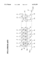
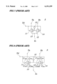
- FIG. 6 is a diagram showing a concept of electrical configurations of important features of a conventional semiconductor memory device disclosed in the above application.
- This semiconductor memory device as shown in FIG. 6, is provided with "n" pieces of memory-cell columns 1 1 to 1 n , each having two or more memory cells. Of these memory-cell columns, the column 1 n is a redundancy memory-cell column.
- Each of the memory-cell columns 1 1 to 1 n is connected to input-output nodes 2 1 to 2 n through each of corresponding bit lines.
- switches 3 1 to 3 n-1 Between the input-output nodes 2 1 to 2 n adjacent to each other are placed "(n-1)" pieces of switches 3 1 to 3 n-1 .
- a terminal Ta of each of these switches 3 1 to 3 n-1 is connected to a left side of each of input-output nodes 2 as shown in the drawing.
- a terminal Tb of each switch 3 is connected to a right side of each of input-output nodes 2 1 to 2 n as shown in the drawing and a terminal Tc of the switch 3 is connected to each of corresponding input-output lines 4 1 to 4 n-1 .
- more than one word line is mounted in the direction of a row to connect each of memory-cell columns 1 1 to 1 n .
- a desired memory cell is selected to allow reading and/or writing.
- circuits including a sense amplifier, column selecting circuit, read/write buffer and the like, required to make the memory cell read or write data.
- FIG. 7 is a circuit diagram of a switch constituting the conventional semiconductor memory device.
- the switch 3 is composed of transfer NMOS transistors (hereinafter referred to as transistors) 11 and 12, transfer PMOS transistors (hereinafter referred to as transistors) 13 and 14 and an inverter 15.
- transistors transfer NMOS transistors
- transistors 13 and 14 transfer PMOS transistors
- inverter 15 When a "high" level control voltage is applied to the terminal Td of the switch 3, the transfer NMOS 11 is turned on and the transfer PMOS 14 is turned off.
- an output voltage of the inverter 15 goes "high", the transfer NMOS 12 is turned off and the transfer PMOS 13 is turned on. This causes the terminal Tc to be connected to the terminal Ta.
- any one of memory cells constituting the memory-cell column 1 4 is a defective memory cell (the memory-cell column containing defective memory cells is referred hereinafter to as a defective memory-cell column)
- a fuse 5 4 is turned off and the terminal Tc of all switches 3 1 to 3 3 disposed on the left side of the memory-cell column 1 4 is connected to the terminal Ta and the switching is made so that the switch can be connected to input-output nodes 2 1 to 2 3 disposed on the left side of these switches and, at the same time, the terminal Tc of all switches 3 4 to 3 n-1 disposed on the right side of the memory-cell column 1 4 is connected to the terminal Tb and the switching is made so that the switch can be connected to input-output nodes 2 4 to 2 n-1 disposed on the right side of these switches.
- the terminal Td of the switch 3 disposed far from the position of the ground GND (for example, the switch 3 1 ) is hardly held at the ground potential and is driven in a state of easily picking up noises occurring in the surrounding atmosphere because of resistance and capacitance of fuses 5 2 to 5 n connected between the switch and the position of the ground GND and of the wiring installed to connect these fuses therewith.
- a gate and drain of the transfer NMOS 11 are coupled respectively to a gate and drain of the transfer NMOS 12 owing to floating capacitance C NGD between the gates and the drains of the transfer NMOSs 11 and 12 (see FIG. 7), while a gate and source of the transfer PMOS 13 are coupled respectively to a gate and source of the transfer PMOS 14 owing to floating capacitance C PGS between the gates and the sources of the transfer PMOSs 13 and 14 (see FIG.
- the gate voltage of each transistor may be changed instantaneously from a "low” to a "high” (this is called “coupling noise”). Because of this, there are some cases where the transfer NMOS 12 and transfer PMOS 14 become in the OFF state though it should be originally in the ON state, while the transfer NMOS 11 and transfer PMOS 13 become in the ON state though it should be originally in the OFF state. Then, if the terminal Ta of the switch 3 1 is once connected to the terminal Ta, data is erroneously written in the defective memory-cell column 1 1 to which data should not be originally written.
- the terminal Td of the switch 3 disposed far from the power source (for example, the switch 3 n-1 ) is hardly held at the supply voltage Vcc and is driven in a state of easily picking up noises occurring in the surrounding atmosphere because of the resistance and capacitance of fuses 5 1 to 5 n connected between the switch 3 and the power source and of the wiring installed to connect these fuses therewith.
- the read-out data may contain values being shifted by one bit, causing malfunctions of equipment employing this semiconductor memory device.
- the value of read data may be entirely different from that of data which should have been stored initially and the malfunction of the equipment using this semiconductor memory device is inevitable.
- a semiconductor memory device comprising:
- input-output lines the number of which is smaller than that of the memory-cell columns
- switches mounted so as to correspond to the input-output lines and to connect, in response to a control voltage, either of the memory-cell columns adjacent to each other to corresponding input-output lines;
- more than one defective-position setting means connected in series, one terminal of which is held at a "high” level potential and the other terminal of which is held at a “high” or “low” level potential, and wherein a voltage of a point of connection between these means is applied, as the control voltage, to two or more switches; and at least one control voltage holding circuit to hold the control voltage supplied to two or more switches at a "high” or “low” level.
- a semiconductor memory device comprising:
- two or more memory-cell column groups each having more than one memory-cell column consisting of two or more memory cells
- column selecting circuits to select, in response to a column address signal, any one of the memory-cell column groups
- more than one defective-position setting means connected in series, one terminal of which is held at a "high” level potential and the other terminal of which is held at a “low” level potential, and wherein a voltage of a point of connection between these means is supplied, as the control voltage, to said two or more switches;
- At least one control voltage holding circuit to hold the control voltage supplied to two or more switches at a "high” or “low” level.
- a preferable mode is one wherein the control voltage holding circuit comprises a first control voltage holding circuit to hold, in accordance with shut-off states of the defective-position setting means disposed in the vicinity of the control voltage holding circuit, the control voltage supplied to the switches to a "high” or “low” level and wherein the control voltage holding circuit is provided for each said point of connection, for every other point of connection or for every predetermined numbers of the point of connection.
- a preferable mode is one wherein the control voltage holding circuit comprises a second control voltage holding circuit to hold the control voltage supplied to the switches at a "high" level and a third control voltage holding circuit to hold the control voltage supplied to the switches at a "low” level, and wherein the second control voltage holding circuit is provided for each point of connection, for every other point of connection or for every predetermined numbers of the point of connection disposed between one end of the line to which the point of connection is coupled and approximate center position of the line, or in the vicinity of the last one of points of connection constituting one third of the total points of connection counted from one end of said line to which the point of connection is coupled, and wherein the third control voltage holding circuit is provided for each point of connection, for every other point of connection or for every predetermined numbers of point of connection disposed between the other end of the line to which the point of connection is coupled and approximate center position of the line, or in the vicinity of the last one of points of connection constituting one third of the total points of connection counted from the other end of the line to which
- a preferable mode is one wherein the first control voltage holding circuit is disposed at a center of the line to which the point of connection is coupled.
- a preferable mode is one wherein the first control voltage holding circuit comprises a first inverter the output terminal of which is connected to a corresponding point of connection and a second inverter the input terminal of which is connected to an output terminal of the first inverter and the output terminal of which is connected to an input terminal of said first inverter.
- a preferable mode is one wherein the second control voltage holding circuit comprises an n-channel MOS transistor the drain of which is connected to a corresponding point of connection and the source voltage of which is held “low” and an inverter the input terminal of which is connected to the drain and the output terminal of which is connected to a gate of the n-channel MOS transistor.
- a preferable mode is one wherein the third control voltage holding circuit comprises a p-channel MOS transistor the drain of which is connected to a corresponding point of connection and the source voltage of which is held "high" and an inverter the input terminal of which is connected to the drain and the output terminal of which is connected to a gate of the p-channel MOS transistor.
- the defective-position setting means is composed of fuses.
- the defective-position setting means is composed of transistors or transfer gates.
- a preferable mode is one wherein the semiconductor memory device comprises a fuse one terminal of which is held at a "high” level potential, a resistor one terminal of which is connected to the fuse and the other terminal of which is held at a "low” level potential, a voltage holding circuit composed of at least one n-channel MOS transistor and of a buffer the input terminal of which is connected to a point of connection between the fuse and the resistor and the other terminal of which is connected to the other terminal of two or more defective-position setting means connected in series and wherein the potential of other terminal of two or more defective-position setting means connected in series is held “high” or “low” by said voltage holding circuit.
- a preferable mode is one wherein the voltage holding circuit has a flip-flop composed of at least two inverters, instead of said buffer.
- a preferable mode is one wherein the inverter comprises an n-channel MOS transistor and p-channel MOS transistor and when SN represents the size of said n-channel MOS transistor constituting the buffer or an n-channel MOS transistor constituting an inverter of the flip-flop, Sp representing the size of a p-channel MOS constituting a first inverter of the first control voltage holding circuit or constituting the third control voltage holding circuit and k representing the number of the first and third control voltage holding circuit, the following formula (1) is satisfied:
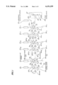
- FIG. 1 is a block diagram showing electrical configurations of important features of the semiconductor memory device according to a first embodiment of the present invention
- FIG. 2 is a circuit diagram showing electrical configurations of a control voltage holding circuit constituting the semiconductor memory device
- FIG. 3 is also a circuit diagram showing electrical configurations of a control voltage holding circuit constituting the semiconductor memory device
- FIG. 4 is a circuit diagram showing electrical configurations of a control voltage holding circuit constituting a semiconductor memory device according to a second embodiment of the present invention.
- FIG. 5 is a block diagram showing electrical configurations of important features of a semiconductor memory device according to a third embodiment of the present invention.
- FIG. 6 is a diagram showing a concept of electrical configurations of important features of a conventional semiconductor memory device
- FIG. 7 is a circuit diagram of a switch constituting the conventional semiconductor memory device.
- FIG. 8 is a circuit diagram to describe shortcomings of the conventional memory device.
- FIG. 1 is a block diagram showing electrical configurations of important features of a semiconductor memory device according to a first embodiment of the present invention.
- the semiconductor memory device is provided with "n" pieces of memory-cell columns 21 1 to 21 n each having two or more memory cells and being connected to each of corresponding input-output nodes 22 1 to 22 n via bit lines; the memory-cell column 21 n being a redundancy memory-cell column. It is also provided with "(n-1)" pieces of switches 23 1 to 23 n-1 , each terminal Ta of these switches 23 being connected to the input-output nodes 22 disposed above the terminal as shown in FIG. 1; each terminal Tb of these switches being connected to a right side of each of the input-output notes 22 as shown in FIG. 1 and each terminal Tc of these switches 23 being connected to each of corresponding input-output lines 24 1 to 24 n-1 . Electrical configurations and operations of these switches 23 are the same as those of the switches 3 in FIG. 6 and descriptions of them are omitted accordingly.
- the semiconductor memory device is provided with "(n-1)" pieces of fuses 25 1 to 25 n-1 , which are all connected in series and to one terminal of which a supply voltage Vcc is applied and the other terminal of which is connected to a voltage holding circuit 26.
- a point of connection between these fuses 25 being adjacent to each other is connected to each terminal Td of the switches 23 and a voltage at the point of connection between these fuses 25 being adjacent to each other is applied to the corresponding switches 23 as a control voltage.
- the voltage holding circuit 26 is adapted to hold the other terminal of the fuse 25 n-1 at the supply voltage Vcc or a ground potential GND, which is composed of a fuse 27, a buffer 28 and a resistor 29.
- a supply voltage Vcc To one terminal of the fuse 27 is applied a supply voltage Vcc and the other terminal of the fuse is connected to the position of the ground GND through the resistor 29.
- An input terminal of the buffer 28 is connected to a point of connection between the fuse 27 and the resistor 29 and an output terminal of the buffer 28 is connected to the other terminal of the fuse 25 n-1 .
- the voltage holding circuit 26 is so operated that it holds the other terminal of the fuse 25 n-1 at the supply voltage Vcc while the fuse remains in the ON state and at the ground potential GND while the fuse is in the OFF state.
- the buffer 28 serves to hold the voltage of the other terminal of the fuse 25 n-1 at a high level when the power is applied to the semiconductor memory device while all the fuses 25 1 to 25 n-1 and the fuse 27 are in the ON state regardless of the length of time required for the power to reach a predetermined voltage, and to put the semiconductor memory -- device into the test mode when any defective memory cell is detected.
- each of the terminal Td of the switches from 23 1 to 23.sub.(n-3)/2 is connected respectively to each of control voltage holding circuits 30 1 to 30.sub.(n-3)/2 and each of the terminal Td of the switches from 23.sub.(n-1)/2 to 23.sub.(n-1) is connected respectively to each of control voltage holding circuits 31.sub.(n-1)/2 to 31.sub.(n-1).
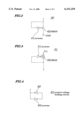
- FIG. 2 is a circuit diagram showing electrical configurations of the control voltage holding circuit 30.
- the control voltage holding circuit 30 is composed of an inverter 41 and a NMOS 42.
- An input terminal of the inverter 41 is connected to the NMOS 42 and a point of connection between these is connected to the terminal Td of the corresponding switch -- 23.
- an output terminal of the inverter 41 is connected to the NMOS 42 and a source of the NMOS is grounded.
- FIG. 3 is a circuit diagram showing electrical configurations of the control voltage holding circuit 31.
- the control voltage holding circuit 31 consists of an inverter 51 and a PMOS 52.
- An input terminal of the inverter 51 is connected to a drain of the PMOS and a point of connection between these is connected to the terminal Td of the corresponding switch 23.
- An output terminal of the inverter 51 is connected to a gate of the PMOS 52 and to a source of the PMOS is applied the supply voltage Vcc.
- a gate and drain of the transfer NMOS 11 are coupled respectively to a gate and drain of the transfer NMOS 12 owing to floating capacitance C NGD of the transfer NMOSs 11 and 12 (see FIG. 7), while a gate and source of the transfer PMOS 13 are coupled respectively to a gate and source of the transfer PMOS 14 owing to floating capacitance C PGS (see FIG. 7).
- a gate and source of the transfer NMOS 11 are coupled to a gate and source of the transfer NMOS 12 owing to floating capacitance C NGS of the transfer NMOSs 11 and 12 (see FIG. 8), while a gate of the transfer PMOS 13 is coupled to a drain of the transfer PMOS 14 owing to floating capacitance C PGD (see FIG. 8).
- the gate and source of the transfer NMOS 11 are coupled respectively to a gate and source of the transfer NMOS 12 owing to floating capacitance C NGS of the transfer NMOSs 11 and 12 (see FIG. 8), while the gate and drain of the transfer PMOS 13 are coupled respectively to the gate and drain of the transfer PMOS 14 owing to floating capacitance C PGD (see FIG. 8).
- control voltage holding circuit 30 is provided to hold the voltage at each terminal Td of switches 23 1 to 23.sub.(n-1)/2 at the ground potential, when the fuse 25 disposed near to the position of the supply voltage Vcc is turned off, coupling noise can be reduced while data are written into the memory-cell column 21 connected to the switch 23 disposed far from the position of the ground GND. By this, a malfunction can be prevented when data are written/read.
- control voltage holding circuit 31 is provided to hold the voltage at each terminal Td of switches 23.sub.(n+1) to 23.sub.(n-1) at the ground potential, when the fuse 25 disposed near to the position of the ground GND is turned off, the coupling noise can be reduced while data are written into the memory-cell column 21 connected to the switch 23 disposed far from the power source Vcc. By this, a malfunction can be prevented when data are written/read.
- FIG. 4 is a circuit diagram showing electrical configurations of a control voltage holding circuit 61 constituting the semiconductor memory device according to a second embodiment of the present invention.
- the control voltage holding circuit 61 is composed of two inverters 62 and 63. An output terminal of the inverter 62 is connected to the input terminal of the inverter 63 and a point of connection between these inverters is connected to the terminal Td of the switch 23. Moreover, an input terminal of the inverter 62 is connected to an output of the inverter 63.
- a gate and a source of the transfer NMOS 11 are coupled respectively to a gate and source of the transfer NMOS 12 owing to floating capacitance C NGS of the transfer NMOSs 11 and 12 (see FIG. 8), while a gate and drain of the transfer PMOS 13 are coupled to a gate and drain of the transfer PMOS 14 owing to floating capacitance C PGD (see FIG. 7).
- the gate and source of the transfer NMOS 11 are coupled respectively to the gate and the source of the transfer NMOS 12 owing to floating capacitance C NGS of the transfer NMOSs 11 and 12 (see FIG. 8), while the gate and drain of the transfer PMOS 13 are coupled respectively to the gate and drain of the transfer PMOS 14 owing to floating capacitance C PGD (see FIG. 8).
- a gate and drain of the transfer NMOS 11 are coupled respectively to a gate and drain of the transfer NMOS 12 owing to floating capacitance C NGD of the transfer NMOSs 11 and 12 (see FIG. 8), while a gate and source of the transfer PMOS 13 are coupled respectively to a gate and source of the transfer PMOS 14 owing to floating capacitance C PGS (see FIG. 8).
- the gate and source of the transfer NMOS 11 are coupled respectively to the gate and the source of the transfer NMOS 12 owing to floating capacitance C NGS of the transfer NMOSs 11 and 12 (see FIG. 8), while the gate and drain of the transfer PMOS 13 are coupled respectively to the gate and drain of the transfer PMOS 14 owing to floating capacitance C PGD (see FIG. 8).
- the control voltage holding circuit 61 is provided to hold the voltage at each terminal Td of switches 23 at the ground potential or at the supply voltage Vcc, when the fuse 25 disposed near to the power source Vcc is turned off, the coupling noise can be reduced while data are written into the memory-cell column 21 connected to the switch 23 disposed far from the position of the ground GND and when the fuse 25 disposed near to the position of the ground GND is turned off, the coupling noise can be reduced while data are written into the memory-cell column 21 connected to the switch 23 disposed far from the power source Vcc. By this, a malfunction can be prevented when data are written/read.
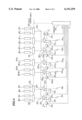
- FIG. 5 is a block diagram showing electrical configurations of important features of the semiconductor memory device according to a third embodiment of the present invention.
- the same reference numbers in FIG. 5 designate corresponding parts in FIG. 1 and the description of the parts is omitted.
- NMOS transistors 33 1 to 33 n are provided as defective-position setting means, instead of the fuses 25 1 to 25 n-1 used in FIG. 1.
- Each source of the NMOS transistors 33 1 to 33 n-1 is connected in series to each drain of the NMOS transistors disposed adjacent to each other.
- the drain of the NMOS transistor 33 1 is connected to the power source Vcc.
- the source of the NMOS transistor 33 n is connected to a ground GND.
- Each gate of the NMOS transistors 33 1 to 33 n is connected to a register 34.
- column selecting circuits 32 1 to 32 n are connected to input-output nodes 22 1 to 22 n .
- To the column selecting circuits 32 1 to 32 n are connected multiple memory-cell column group 20 1 to 20 n and 21 1 to 21 n .
- the column selecting circuits 32 1 to 32 n are adapted to select either the memory-cell column group 20 1 to 20 n or the memory-cell column group 21 1 to 21 n in response to a column address signal and to connect the selected memory-cell column group to the input-output nodes 22 1 to 22 n .
- the register 34 prestores setting signals r 1 to r n to turn off any one of the transistors 33 1 to 33 n and to turn on other remaining transistors.
- the setting signals r 1 to r n correspond to the register column the number of which is equivalent to that of the memory-cell column group.
- the register 34 selects one of the register columns in response to the column address signal and outputs the setting signal.
- two memory-cell column groups are provided, two register columns are mounted and the switching can be performed by one column address signal. If, for example, four memory-cell column groups are provided per one input-output line, four register-columns may be mounted and switching may be made by two column address signals accordingly.
- the register 34 reads out the signals "011 . . . 11" as the setting signal from the first register columns r11 to rn1 and feeds them to a gate of each of the transistors 33 1 to 33 n . This causes the transistor 33 1 to be off and transistors 33 2 to 33 n to be turned on and, as a result, all the control voltages go "low". Since the subsequent operations are the same as those in the first embodiment, their description is omitted.
- the register 34 reads out the signals "111 . . . 10" as the setting signal from the second register columns r12 to rn2 and feeds them to the gate of each of transistors 33 1 to 33 n .
- This causes the transistor 33 n to be on and transistors 33 1 to 33 n-1 to be turned off and, as a result, all the control voltages go "high". Since the subsequent operations are the same as those in the first embodiment, their description is omitted.
- a redundancy circuit can be constructed by using only one set of the switches 23 1 to 23 n-1 to cover two or more memory-cell column groups, allowing the reduction of a chip area of the semiconductor memory device as well as the reduction of the fraction defective, i.e., the maximum use of non-defective memory-cell columns other than defective one or ones occurred in one semiconductor memory device.
- the NMOS transistors are used as the transistors 33 1 to 33 n , however, PMOS transistors may be used by appropriately setting a logical level of a potential to be supplied to the gate, or a transfer gate may be employed as well. Also, as in the second embodiment, the grounding position or types of switches as well as the voltage holding circuit 61 can be changed appropriately so as to be the most suited ones.
- the control voltage holding circuit is provided for each switch 23. However, it may be provided for every other switch or for every predetermined numbers of switches. Or, the control voltage holding circuit 30 or 61 may be connected to the terminal Td of the switch 23, out of (n-1) switches 23 1 to 23 n-1 , placed between the position of the supply voltage Vcc and the center position on a horizontal line, for example, in the vicinity of the last one of switches constituting one third of the total switches counted from the side of the power source Vcc.
- control voltage holding circuit 31 or 61, or both the circuits 31 and 61 may be connected to the terminal Td of the switch 23 placed between the voltage holding circuit 26 and the center position on the horizontal line, for example, in the vicinity of the last one of switches constituting one third of the total switches counted from the side of the voltage holding circuit 26.
- control voltage holding circuit 61 may be connected to the terminal Td of the switch 23 placed approximately in the center of the horizontal line.
- the semiconductor memory device is provided with a single input-output line for 1 bit of data, however, the invention is not limited to this.
- it may be provided with a complementary input-output for 1 bit of data as in the case of a DRAM or SRAM fabricated with CMOS technology where the complementary input-output line is introduced.
- the present invention can be applied to a semiconductor memory device composed of more than one memory block consisting of two or more memory-cell columns and redundancy memory-cell columns.
- the voltage holding circuit 26 is composed of the fuse 27, buffer 28 and resistor 29.
- the voltage holding circuit 26 can be constructed without using the buffer 28, and can also be configured using a flip flop consisting of two inverters, instead of the buffer. The use of the flip flop can give more efficient effects to the voltage holding circuit at power-on.
- the voltage holding circuit 26 may be so configured that a supply voltage Vcc is applied to one terminal of a resistor, to the other terminal of which one terminal of a fuse is connected and the other terminal of the fuse is grounded.
- SN represents the size of the NMOS constituting the buffer 28
- Sp representing the size of the PMOS constituting the PMOS 52 or the inverter 62
- k representing the number of the control voltage holding circuit 31 and 61 mounted therein.
- the supply voltage Vcc from the leftmost position in the drawing and to the fuses placed in the rightmost position is connected the voltage holding circuit 26.
- the voltage holding circuit 26 may be connected to the fuse placed in the leftmost position in the drawing and the supply voltage Vcc may be applied to the fuse from the rightmost position.
- the supply voltage Vcc or the ground GND is not necessarily required as a potential to be applied to the fuses connected in series or the voltage holding circuit 26, and simply a "high” or “low” voltage may be used if only the applied voltage can serve to connect the terminal Tc of the switch 23 to the terminal Ta or Tb.
Abstract
Description
2·SN≧kSp (1)
2·SN≧k·Sp (2)
Claims (17)
2·SN≧k·Sp (3).
2·SN≧k·Sp (4).
Applications Claiming Priority (2)
| Application Number | Priority Date | Filing Date | Title |
|---|---|---|---|
| JP10-262109 | 1998-09-16 | ||
| JP26210998A JP3178430B2 (en) | 1998-09-16 | 1998-09-16 | Semiconductor storage device |
Publications (1)
| Publication Number | Publication Date |
|---|---|
| US6151259A true US6151259A (en) | 2000-11-21 |
Family
ID=17371171
Family Applications (1)
| Application Number | Title | Priority Date | Filing Date |
|---|---|---|---|
| US09/396,211 Expired - Lifetime US6151259A (en) | 1998-09-16 | 1999-09-15 | Semiconductor memory device |
Country Status (4)
| Country | Link |
|---|---|
| US (1) | US6151259A (en) |
| JP (1) | JP3178430B2 (en) |
| KR (1) | KR100299001B1 (en) |
| TW (1) | TW440856B (en) |
Cited By (4)
| Publication number | Priority date | Publication date | Assignee | Title |
|---|---|---|---|---|
| US6507524B1 (en) * | 2000-11-30 | 2003-01-14 | Lsi Logic Corporation | Integrated circuit memory having column redundancy |
| US6639855B2 (en) * | 2001-11-14 | 2003-10-28 | Fujitsu Limited | Semiconductor device having a defect relief function of relieving a failure |
| KR100884007B1 (en) * | 2002-05-22 | 2009-02-17 | 후지쯔 마이크로일렉트로닉스 가부시키가이샤 | Semiconductor device |
| US10783954B2 (en) * | 2015-12-17 | 2020-09-22 | Taiwan Semiconductor Manufacturing Co., Ltd. | Semiconductor memory with respective power voltages for memory cells |
Families Citing this family (1)
| Publication number | Priority date | Publication date | Assignee | Title |
|---|---|---|---|---|
| JP6360610B1 (en) | 2017-11-22 | 2018-07-18 | 力晶科技股▲ふん▼有限公司 | Redundant circuit for SRAM device, SRAM device, and semiconductor device |
Citations (3)
| Publication number | Priority date | Publication date | Assignee | Title |
|---|---|---|---|---|
| US4672240A (en) * | 1983-02-07 | 1987-06-09 | Westinghouse Electric Corp. | Programmable redundancy circuit |
| JPH07122096A (en) * | 1990-09-28 | 1995-05-12 | Intergraph Corp | High-speed redundant row and column for semiconductor memory |
| US5715202A (en) * | 1994-12-22 | 1998-02-03 | Kabushiki Kaisha Toshiba | Semiconductor memory device |
-
1998
- 1998-09-16 JP JP26210998A patent/JP3178430B2/en not_active Expired - Fee Related
-
1999
- 1999-09-14 TW TW088115949A patent/TW440856B/en not_active IP Right Cessation
- 1999-09-15 US US09/396,211 patent/US6151259A/en not_active Expired - Lifetime
- 1999-09-16 KR KR1019990039759A patent/KR100299001B1/en not_active IP Right Cessation
Patent Citations (3)
| Publication number | Priority date | Publication date | Assignee | Title |
|---|---|---|---|---|
| US4672240A (en) * | 1983-02-07 | 1987-06-09 | Westinghouse Electric Corp. | Programmable redundancy circuit |
| JPH07122096A (en) * | 1990-09-28 | 1995-05-12 | Intergraph Corp | High-speed redundant row and column for semiconductor memory |
| US5715202A (en) * | 1994-12-22 | 1998-02-03 | Kabushiki Kaisha Toshiba | Semiconductor memory device |
Cited By (6)
| Publication number | Priority date | Publication date | Assignee | Title |
|---|---|---|---|---|
| US6507524B1 (en) * | 2000-11-30 | 2003-01-14 | Lsi Logic Corporation | Integrated circuit memory having column redundancy |
| US6639855B2 (en) * | 2001-11-14 | 2003-10-28 | Fujitsu Limited | Semiconductor device having a defect relief function of relieving a failure |
| KR100865340B1 (en) * | 2001-11-14 | 2008-10-27 | 후지쯔 마이크로일렉트로닉스 가부시키가이샤 | Semiconductor device |
| KR100884007B1 (en) * | 2002-05-22 | 2009-02-17 | 후지쯔 마이크로일렉트로닉스 가부시키가이샤 | Semiconductor device |
| US10783954B2 (en) * | 2015-12-17 | 2020-09-22 | Taiwan Semiconductor Manufacturing Co., Ltd. | Semiconductor memory with respective power voltages for memory cells |
| US11264088B2 (en) | 2015-12-17 | 2022-03-01 | Taiwan Semiconductor Manufacturing Co., Ltd. | Semiconductor memory with respective power voltages for memory cells |
Also Published As
| Publication number | Publication date |
|---|---|
| JP2000090687A (en) | 2000-03-31 |
| TW440856B (en) | 2001-06-16 |
| KR100299001B1 (en) | 2001-11-07 |
| KR20000023200A (en) | 2000-04-25 |
| JP3178430B2 (en) | 2001-06-18 |
Similar Documents
| Publication | Publication Date | Title |
|---|---|---|
| KR950007456B1 (en) | Redundant circuit | |
| US8711614B1 (en) | Memory elements with increased write margin and soft error upset immunity | |
| US5406516A (en) | Semiconductor memory device | |
| US7345945B2 (en) | Line driver circuit for a semiconductor memory device | |
| KR20100082046A (en) | Asynchronous multi-bit otp memory cell and asynchronous multi-bit otp memory device, programming method and read out method of the same | |
| US9412436B1 (en) | Memory elements with soft error upset immunity | |
| US4987560A (en) | Semiconductor memory device | |
| US6262924B1 (en) | Programmable semiconductor memory device | |
| JPH1011993A (en) | Semiconductor memory device | |
| US5446700A (en) | Decoder circuit having CMOS inverter circuits | |
| US4641285A (en) | Line change-over circuit and semiconductor memory using the same | |
| US6501817B2 (en) | Area efficient redundancy multiplexer circuit technique for integrated circuit devices providing significantly reduced parasitic capacitance | |
| US7924605B2 (en) | Semiconductor memory device | |
| US5696716A (en) | Programmable memory element | |
| EP0419760A2 (en) | Zero standby power, radiation hardened, memory redundancy circuit | |
| US6151259A (en) | Semiconductor memory device | |
| KR950000029B1 (en) | Decoder circuit of eprom for avoiding erronous operation caused by parastic capacitors | |
| US6269033B1 (en) | Semiconductor memory device having redundancy unit for data line compensation | |
| KR100454118B1 (en) | Semiconductor memory device and test method thereof | |
| US5299163A (en) | Semiconductor memory device with discriminator for diagnostic mode of operation | |
| US8014212B2 (en) | Semiconductor device and control method thereof | |
| US7639557B1 (en) | Configurable random-access-memory circuitry | |
| US6982912B2 (en) | Semiconductor memory device | |
| US20030026124A1 (en) | Semiconductor memory device | |
| US5293561A (en) | Write-in voltage source incorporated in electrically erasable programmable read only memory device with redundant memory cell array |
Legal Events
| Date | Code | Title | Description |
|---|---|---|---|
| AS | Assignment |
Owner name: NEC CORPORATION, JAPAN Free format text: ASSIGNMENT OF ASSIGNORS INTEREST;ASSIGNOR:HORI, MINEYUKI;REEL/FRAME:010252/0848 Effective date: 19990906 |
|
| STCF | Information on status: patent grant |
Free format text: PATENTED CASE |
|
| FEPP | Fee payment procedure |
Free format text: PAYOR NUMBER ASSIGNED (ORIGINAL EVENT CODE: ASPN); ENTITY STATUS OF PATENT OWNER: LARGE ENTITY |
|
| AS | Assignment |
Owner name: NEC ELECTRONICS CORPORATION, JAPAN Free format text: ASSIGNMENT OF ASSIGNORS INTEREST;ASSIGNOR:NEC CORPORATION;REEL/FRAME:013751/0721 Effective date: 20021101 |
|
| FPAY | Fee payment |
Year of fee payment: 4 |
|
| FPAY | Fee payment |
Year of fee payment: 8 |
|
| AS | Assignment |
Owner name: RENESAS ELECTRONICS CORPORATION, JAPAN Free format text: CHANGE OF NAME;ASSIGNOR:NEC ELECTRONICS CORPORATION;REEL/FRAME:025375/0948 Effective date: 20100401 |
|
| FPAY | Fee payment |
Year of fee payment: 12 |
|
| AS | Assignment |
Owner name: RENESAS ELECTRONICS CORPORATION, JAPAN Free format text: CHANGE OF ADDRESS;ASSIGNOR:RENESAS ELECTRONICS CORPORATION;REEL/FRAME:044928/0001 Effective date: 20150806 |