US6151667A - Telecommunication device, more particularly, mobile radio terminal - Google Patents
Telecommunication device, more particularly, mobile radio terminal Download PDFInfo
- Publication number
- US6151667A US6151667A US08/931,396 US93139697A US6151667A US 6151667 A US6151667 A US 6151667A US 93139697 A US93139697 A US 93139697A US 6151667 A US6151667 A US 6151667A
- Authority
- US
- United States
- Prior art keywords
- address
- counter
- processor
- bus
- telecommunication device
- Prior art date
- Legal status (The legal status is an assumption and is not a legal conclusion. Google has not performed a legal analysis and makes no representation as to the accuracy of the status listed.)
- Expired - Lifetime
Links
Images
Classifications
-
- H—ELECTRICITY
- H04—ELECTRIC COMMUNICATION TECHNIQUE
- H04W—WIRELESS COMMUNICATION NETWORKS
- H04W88/00—Devices specially adapted for wireless communication networks, e.g. terminals, base stations or access point devices
- H04W88/02—Terminal devices
-
- Y—GENERAL TAGGING OF NEW TECHNOLOGICAL DEVELOPMENTS; GENERAL TAGGING OF CROSS-SECTIONAL TECHNOLOGIES SPANNING OVER SEVERAL SECTIONS OF THE IPC; TECHNICAL SUBJECTS COVERED BY FORMER USPC CROSS-REFERENCE ART COLLECTIONS [XRACs] AND DIGESTS
- Y02—TECHNOLOGIES OR APPLICATIONS FOR MITIGATION OR ADAPTATION AGAINST CLIMATE CHANGE
- Y02D—CLIMATE CHANGE MITIGATION TECHNOLOGIES IN INFORMATION AND COMMUNICATION TECHNOLOGIES [ICT], I.E. INFORMATION AND COMMUNICATION TECHNOLOGIES AIMING AT THE REDUCTION OF THEIR OWN ENERGY USE
- Y02D30/00—Reducing energy consumption in communication networks
- Y02D30/70—Reducing energy consumption in communication networks in wireless communication networks
Definitions
- the invention relates to a telecommunication device, more particularly, a mobile radio terminal, comprising at least one processor for processing data, to which processor at least one data memory is assigned which is coupled to the processor via data and address lines of a bus system.
- processors and data memories are coupled to each other by bus systems which have a certain number of data lines and address lines depending on the system configuration.
- the bus systems also have control lines over which control signals are exchanged between the processors and the data memories.
- microprocessors or signal processors are used as processors here.
- data memories used are RAM, ROM, EPROM and Flash EPROM.
- One processor may be assigned various data memories to which the processor has access. For loading data of a data memory, the respective processor applies addresses to the address lines of the bus system and transmits them to the data memory. The data memory then transmits the associated data over the data lines of the bus system to the processor.
- the addressing over the data lines of the bus system is effected at the cost of a power consumption that is considerable for many applications.
- the power consumption especially in telecommunication devices using a battery or an accumulator as an energy source, is a critical magnitude (for example, for mobile terminals).
- the addressing over data bus address lines leads to certain minimum data memory access times of a processor, so that the speed with which the program runs can be carried out by the processor is restricted accordingly.
- a first address counter is assigned to the data memory, in that the first address counter is used for delivering addresses to the data memory and in that means are provided which effect an initialization of the first address counter by a transmission of an address generated by the processor over the bus system to the first address counter in the case where an address generated by the first address counter differs from an address generated in parallel by the processor.
- the first address counter produces the addresses necessary for addressing the data memory.
- the count of the first address counter and thus the address produced thereby are adapted to the address produced by the processor.
- the adaptation is effected by initialization of the address counter and subsequent change of the count.
- the address counter is to be initialized when there is a difference between two subsequent addresses produced by the processor, which difference exceeds an incrementation or decrementation step of the first counter, ie when there is an address jump.
- the address change may be made by simply adapting the count of the first address counter.
- the adaptation may be effected by transmitting a control signal of the processor address logic over a single control line to the first address counter.
- the power consumption of the telecommunication device may be reduced, because addressing over parallel address lines is replaced by transmitting the control signal to the first address counter for incrementing and decrementing same and by supplying the address generated by the first address counter without utilizing the address lines of the bus system, which costs less power.
- the access time to the data memory is reduced, because generating new addresses by changing the count of the first address counter and addressing the data memory by the addresses thus generated by the first address counter requires less time than the conventional addressing over the address lines of the bus system of the telecommunication device.
- the increased processing speed may be further increased by a cache memory arranged in the processor.
- the processor is assigned a second address counter, and means are provided for the parallel initialization and parallel change of the counts of the first and second address counters.
- the processor With the second address counter, the processor has a means available with which it can simulate the count of the first address counter. Whether a transmission of an address to the first address counter over the address lines of the bus system is necessary may be established by evaluation of the second address counter in the processor, which thus leads to little circuitry and cost.
- a comparator unit is provided, which is used for comparing the addresses generated by the processor with the counts of the second address counter and causes the respective address generated by the processor to be loaded into the second address counter and over the bus system into the first address counter when a difference is found between two compared values.
- the comparator unit undertakes to make the comparisons and carry out control functions or transmitting an address to the first address counter.
- the addressing of the data memory can be carried out faster. The cost of hardware for realizing this embodiment is low.
- a serial transmission of address data over the bus system to the first address counter makes it possible to save on address lines.
- this advantage is at the expense of more time for the transmission of the address over the bus system.
- the data memory and the first address counter and/or, on the other hand, also the processor, the second address counter and the comparator unit are arranged on one common chip, so that the arrangement of the telecommunication device according to the invention is realized cost effectively and with the fewest possible separate components when mass produced.
- the number of address lines of the bus system is smaller than the number of address bits per address, that a certain number of most significant address bits of an address are transmitted to the first address counter and that, subsequently, the count of the first address counter is changed via control signals generated by the processor logic so as to reconstruct the least significant address bits which have not been transmitted.
- the reduced number of address lines which are necessary for a more cost-effective realization of the bus system and for a reduced power consumption of the telecommunication device, the access time increases by leaps and bounds, compared to the conventional devices which process the same address lengths.
- the reconstruction of the address bits not transmitted by address lines to the first address counter and thus to the data memory, by the change of the count of the first counter via control signals which may be transmitted over a single separate control line, however, is fast and needs only little control circuitry.
- the invention likewise relates to a method of addressing a data memory by means of a processor which is coupled to the data memory via a bus system.
- the method implies that an address counter assigned to the data memory delivers addresses to the data memory and that, in the case where a current address generated by the address counter differs from an address generated in parallel by the processor, the address counter is initialized in that the current address generated by the processor is transmitted to the address counter over the bus system.
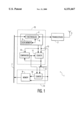
- the FIGURE shows a telecommunication device according to the invention.
- the telecommunication device 1 shown in the FIGURE is arranged here as a mobile radio terminal. It comprises a transceiver 2 to which a transceiver antenna 3 is connected.
- the transceiver 2 communicates with a processor 4 which may be arranged, for example, as a microprocessor or a signal processor.
- the processor 4 is used for processing receive signals received by the transceiver 2 and transmit signals transmitted by the transceiver 2.
- the processor represents a central controller controlling the functions of the telecommunication device 1 and includes a cache memory 5 which communicates with the further units of the processor 4 combined to a function block 6.
- the cache memory 5 is used as a buffer memory and accelerates in customary fashion the control functions and the signal/data processing of the processor 4.
- the program/cache memory allows of returns to the internal cash memory, without the necessity of accessing an external data memory 9 again.
- the telecommunication device 1 includes a bus system formed by a data bus 7 and an address bus 8. They are shown in bold lines for clarity.
- the bus system further includes a control bus (not shown) over whose control lines the processor 4 exchanges control signals with other components of the telecommunication device.
- the telecommunication device 1 includes a data memory 9 already mentioned, for storing data necessary for executing programs. For reading data, the data memory 9 is addressed by the processor 4, which will be further explained hereinafter.
- the telecommunication device 1 arranged as a mobile radio terminal comprises a plurality of processors, in this case a microprocessor and a signal processor. Furthermore, it includes here a plurality of data memories (RAM memory, EPROM memory and Flash EPROM memory). To represent the principle of the invention, however, it is sufficient to refer only to a single processor 4 and a single data memory 9.
- the data memory 9 is assigned a first address counter 10 whose counts are applied as addresses to the data memory 9.
- Processor 4 are assigned a second address counter 11 and a comparator unit 12 to which elements the processor 4 applies addresses in parallel.
- the comparator unit 12 compares the addresses generated by the processor with the respective count of the address counter 11. For the case where the count of the address counter 11 does not exactly match the address produced by the processor 4, the comparator unit 12 applies a control signal both to the second address counter 11 and to the first address counter 10, which control signal causes an address that has just been generated by the processor to be loaded into the two address counters 10 and 11 (initialization of the address counters 10 and 11).
- the address generated by the processor 4 is then loaded into the address counter 11 and converted into a respective count of the address counter 11. This address is loaded into the address counter 10 over the address bus 8.
- the output of the address counter 11 is in the present case coupled to the address bus 8, while the input of the address counter 10 is coupled to the address bus 8.
- the comparator unit 12 For all cases where the comparator unit 12 establishes that the address produced by the processor 4 matches the count of the address counter 11, this comparator unit neither effects an initialization of the address counters 10 and 11, nor a transmission of an address over the address bus as described above. This is always the case when two addresses generated successively by the processor do not imply a leap of address, ie the new address of a respective pair of addresses is the result of a simple incrementation or decrementation of the old address. For such cases which essentially occur more frequently than program leaps in program runs, the address counter 10 simulates the generation of an address by the processor 4, ie its count correctly shows the address generated by the processor 4. The same holds for the address counter 11.
- the address counters 10 and 11 are supplied with a control signal over a control line 13 each time an address is generated by the processor 4, which control signal causes the address counters 10 and 11 to increment or decrement.
- a control signal applied to the address counters 10 and 11 over the control line 13 is at the same time applied to the data memory 9, so that a data word belonging to the address produced by the address counter 10 is read out and this data word is transmitted by the data bus 7 to the processor 4, which further processes the transmitted data word.
- the power consumption of the telecommunication device 1, which power consumption is determined by the addressing of the data memory 9, can be reduced, because the data memory 9 is only addressed over the address bus 8 when the address counters 10 and 11 are initialized.
- the address bus is not used and the address lines may remain deactivated and save energy.
- the access times to the data memory 9 are reduced, because when addressing takes place without the use of address bus 8, the customary address control measures, for controlling the transmission of addresses by the address bus 8, may be omitted.
- a further embodiment of the invention may be provided in that the number of address lines of the address bus 8 are reduced. The number of address lines are then smaller than the number of address bits per address word.
- the address counters 10 and 11 are initialized, a predefined number of most significant address bits are transmitted over the address bus 8. For reconstructing the least significant and not transmitted address bits of an address with which the address counters 10 and 11 are to be initialized, there is thus provided that control signals generated by the processor 4 are transmitted to the address counters 10 and 11 over the control line 13, which control signals cause incrementation and decrementation steps to be effected in accordance with the desired address with which the address counters 10 and 11 are to be initialized.
- the control signals used are then bordered by two control signals which control the data memory 9 in such a way that data are not read from the data memory 9 during the reconstruction of the least significant address bits.
- the reduced number of address lines only leads to an accordingly reduced number of connections via which address bits are applied to the address bus or via which address bits transmitted over the address bus 8 are received.
- the data memory 9 and the address counter 10 are arranged on a common chip 14.
- the processor 4, the address counter 11 and the comparator unit 12 form part of a common chip 15.
- the expenditure and hardware for realizing the address counters 10 and 11 and the comparator unit 12 are then reduced especially when the telecommunication device 1 is mass produced.
- the chips 14 and 15 may be realized in a more compact way because of a reduced number of pins, so that their required space is reduced.
Abstract
Description
Claims (18)
Applications Claiming Priority (2)
| Application Number | Priority Date | Filing Date | Title |
|---|---|---|---|
| DE19638772 | 1996-09-21 | ||
| DE19638772A DE19638772A1 (en) | 1996-09-21 | 1996-09-21 | Telecommunication device, in particular mobile radio terminal |
Publications (1)
| Publication Number | Publication Date |
|---|---|
| US6151667A true US6151667A (en) | 2000-11-21 |
Family
ID=7806467
Family Applications (1)
| Application Number | Title | Priority Date | Filing Date |
|---|---|---|---|
| US08/931,396 Expired - Lifetime US6151667A (en) | 1996-09-21 | 1997-09-16 | Telecommunication device, more particularly, mobile radio terminal |
Country Status (4)
| Country | Link |
|---|---|
| US (1) | US6151667A (en) |
| EP (1) | EP0831666A3 (en) |
| JP (1) | JP4005675B2 (en) |
| DE (1) | DE19638772A1 (en) |
Cited By (3)
| Publication number | Priority date | Publication date | Assignee | Title |
|---|---|---|---|---|
| US6400633B1 (en) * | 2000-02-11 | 2002-06-04 | Advanced Micro Devices, Inc. | Power-saving modes for memories |
| US20090257527A1 (en) * | 2008-04-14 | 2009-10-15 | Wolfram Kluge | Transmission circuit, transmission method, and use |
| US8693679B1 (en) * | 2010-07-22 | 2014-04-08 | Adtran, Inc. | Communications system and associated method for reducing power consumption of a telecommunications device |
Families Citing this family (1)
| Publication number | Priority date | Publication date | Assignee | Title |
|---|---|---|---|---|
| DE102015007331B4 (en) | 2015-06-12 | 2021-07-01 | Psg Germany Gmbh | Double diaphragm pump |
Citations (13)
| Publication number | Priority date | Publication date | Assignee | Title |
|---|---|---|---|---|
| EP0020908A1 (en) * | 1979-06-18 | 1981-01-07 | International Business Machines Corporation | Data processing system comprising a common bus communication system in which the width of the address field is greater than the number of lines on the bus |
| US4347618A (en) * | 1980-06-30 | 1982-08-31 | Stephen P. Kavouras | Apparatus for processing weather radar information |
| US4479178A (en) * | 1981-07-02 | 1984-10-23 | Texas Instruments Incorporated | Quadruply time-multiplex information bus |
| US4484261A (en) * | 1981-01-19 | 1984-11-20 | Texas Instruments Incorporated | Data processing system having interlinked fast and slow memory means and interlinked program counters |
| US5278839A (en) * | 1990-04-18 | 1994-01-11 | Hitachi, Ltd. | Semiconductor integrated circuit having self-check and self-repair capabilities |
| US5307471A (en) * | 1990-01-31 | 1994-04-26 | Nec Corporation | Memory controller for sub-memory unit such as disk drives |
| US5367657A (en) * | 1992-10-01 | 1994-11-22 | Intel Corporation | Method and apparatus for efficient read prefetching of instruction code data in computer memory subsystems |
| US5390333A (en) * | 1990-02-06 | 1995-02-14 | Alcatel Network Systems, Inc. | Switch array power reduction apparatus |
| US5440299A (en) * | 1993-10-01 | 1995-08-08 | Motorola, Inc. | Method and apparatus for equalizing battery life in a selective call communication system |
| WO1995028677A1 (en) * | 1994-04-13 | 1995-10-26 | Ericsson Inc. | Efficient addressing of large memories |
| US5812559A (en) * | 1991-10-02 | 1998-09-22 | Fujitsu Limited | Controlling method and apparatus for examination of multiport RAM(s) |
| US5892978A (en) * | 1996-07-24 | 1999-04-06 | Vlsi Technology, Inc. | Combined consective byte update buffer |
| US5933859A (en) * | 1995-05-19 | 1999-08-03 | Micron Electronics, Inc. | Processor to memory interface logic for use in a computer system using a multiplexed memory address |
-
1996
- 1996-09-21 DE DE19638772A patent/DE19638772A1/en not_active Withdrawn
-
1997
- 1997-09-15 EP EP97202819A patent/EP0831666A3/en not_active Withdrawn
- 1997-09-16 US US08/931,396 patent/US6151667A/en not_active Expired - Lifetime
- 1997-09-19 JP JP25489697A patent/JP4005675B2/en not_active Expired - Lifetime
Patent Citations (13)
| Publication number | Priority date | Publication date | Assignee | Title |
|---|---|---|---|---|
| EP0020908A1 (en) * | 1979-06-18 | 1981-01-07 | International Business Machines Corporation | Data processing system comprising a common bus communication system in which the width of the address field is greater than the number of lines on the bus |
| US4347618A (en) * | 1980-06-30 | 1982-08-31 | Stephen P. Kavouras | Apparatus for processing weather radar information |
| US4484261A (en) * | 1981-01-19 | 1984-11-20 | Texas Instruments Incorporated | Data processing system having interlinked fast and slow memory means and interlinked program counters |
| US4479178A (en) * | 1981-07-02 | 1984-10-23 | Texas Instruments Incorporated | Quadruply time-multiplex information bus |
| US5307471A (en) * | 1990-01-31 | 1994-04-26 | Nec Corporation | Memory controller for sub-memory unit such as disk drives |
| US5390333A (en) * | 1990-02-06 | 1995-02-14 | Alcatel Network Systems, Inc. | Switch array power reduction apparatus |
| US5278839A (en) * | 1990-04-18 | 1994-01-11 | Hitachi, Ltd. | Semiconductor integrated circuit having self-check and self-repair capabilities |
| US5812559A (en) * | 1991-10-02 | 1998-09-22 | Fujitsu Limited | Controlling method and apparatus for examination of multiport RAM(s) |
| US5367657A (en) * | 1992-10-01 | 1994-11-22 | Intel Corporation | Method and apparatus for efficient read prefetching of instruction code data in computer memory subsystems |
| US5440299A (en) * | 1993-10-01 | 1995-08-08 | Motorola, Inc. | Method and apparatus for equalizing battery life in a selective call communication system |
| WO1995028677A1 (en) * | 1994-04-13 | 1995-10-26 | Ericsson Inc. | Efficient addressing of large memories |
| US5933859A (en) * | 1995-05-19 | 1999-08-03 | Micron Electronics, Inc. | Processor to memory interface logic for use in a computer system using a multiplexed memory address |
| US5892978A (en) * | 1996-07-24 | 1999-04-06 | Vlsi Technology, Inc. | Combined consective byte update buffer |
Cited By (4)
| Publication number | Priority date | Publication date | Assignee | Title |
|---|---|---|---|---|
| US6400633B1 (en) * | 2000-02-11 | 2002-06-04 | Advanced Micro Devices, Inc. | Power-saving modes for memories |
| US20090257527A1 (en) * | 2008-04-14 | 2009-10-15 | Wolfram Kluge | Transmission circuit, transmission method, and use |
| US8041316B2 (en) * | 2008-04-14 | 2011-10-18 | Atmel Corporation | Transmission circuit, transmission method, and use |
| US8693679B1 (en) * | 2010-07-22 | 2014-04-08 | Adtran, Inc. | Communications system and associated method for reducing power consumption of a telecommunications device |
Also Published As
| Publication number | Publication date |
|---|---|
| EP0831666A3 (en) | 2000-04-12 |
| EP0831666A2 (en) | 1998-03-25 |
| JPH10136050A (en) | 1998-05-22 |
| JP4005675B2 (en) | 2007-11-07 |
| DE19638772A1 (en) | 1998-03-26 |
Similar Documents
| Publication | Publication Date | Title |
|---|---|---|
| US6002638A (en) | Memory device having a switchable clock output and method therefor | |
| US4694394A (en) | Microprocessor system having a multiplexed address/data bus which communicates with a plurality of memory and input/output devices including TTL output gates | |
| US5345573A (en) | High speed burst read address generation with high speed transfer | |
| KR100390058B1 (en) | Communication system with a master station and at least one slave station | |
| US6483183B1 (en) | Integrated circuit (IC) package with a microcontroller having an n-bit bus and up to n-pins coupled to the microcontroller | |
| US6151667A (en) | Telecommunication device, more particularly, mobile radio terminal | |
| KR960035290A (en) | Method and apparatus for bus loading distribution in a data processing system | |
| CN101310231A (en) | Serial bus system, node device and an input/output card that can be connected to the node device | |
| US5893923A (en) | Microcontroller utilizing a circuit to select during reset process an internal or external memory as base memory | |
| US5214423A (en) | Random number generation using volatile RAM | |
| US6138188A (en) | Buffer management device and method for improving buffer usage and access performance in data processing system | |
| US6874013B2 (en) | Data processing arrangement and memory system | |
| US7020730B2 (en) | Method for operating a microprocessor configuration and microprocessor configuration | |
| US7457171B2 (en) | Integrated semiconductor memory with transmission of data via a data interface | |
| US6795911B1 (en) | Computing device having instructions which access either a permanently fixed default memory bank or a memory bank specified by an immediately preceding bank selection instruction | |
| US5307475A (en) | Slave controller utilizing eight least/most significant bits for accessing sixteen bit data words | |
| US6240496B1 (en) | Architecture and configuring method for a computer expansion board | |
| US6597690B1 (en) | Method and apparatus employing associative memories to implement limited switching | |
| EP0352806A2 (en) | Cache memory and access controller using such memory | |
| US6480910B1 (en) | Digital interface unit with selective input registers providing control values to output registers that simultaneously output the control values when activated by control line | |
| US5357619A (en) | Paged memory scheme | |
| KR0175606B1 (en) | Data interface apparatus between pc main processor and pc card | |
| KR100664334B1 (en) | Data processing arrangement and memory system | |
| US5355458A (en) | Microcomputer with table address forcing for different size memories | |
| KR0174509B1 (en) | Apparatus for controlling access mode of memory and method |
Legal Events
| Date | Code | Title | Description |
|---|---|---|---|
| AS | Assignment |
Owner name: U.S. PHILIPS CORPORATION, NEW YORK Free format text: ASSIGNMENT OF ASSIGNORS INTEREST;ASSIGNOR:WALTERS, ECKHARD;REEL/FRAME:008947/0740 Effective date: 19971020 |
|
| STCF | Information on status: patent grant |
Free format text: PATENTED CASE |
|
| FPAY | Fee payment |
Year of fee payment: 4 |
|
| AS | Assignment |
Owner name: NXP B.V., NETHERLANDS Free format text: ASSIGNMENT OF ASSIGNORS INTEREST;ASSIGNOR:U.S. PHILIPS CORPORATION;REEL/FRAME:018635/0755 Effective date: 20061127 |
|
| FPAY | Fee payment |
Year of fee payment: 8 |
|
| FPAY | Fee payment |
Year of fee payment: 12 |
|
| AS | Assignment |
Owner name: ERICSSON MODEMS SA, SWITZERLAND Free format text: ASSIGNMENT OF ASSIGNORS INTEREST;ASSIGNORS:NXP B.V.;ST WIRELESS SA;ST-ERICSSON SA;SIGNING DATES FROM 20080714 TO 20130802;REEL/FRAME:033215/0430 |
|
| AS | Assignment |
Owner name: ERICSSON MODEMS SA, SWITZERLAND Free format text: CORRECTIVE ASSIGNMENT TO CORRECT THE ASSIGNORS PREVIOUSLY RECORDED ON REEL 033215 FRAME 0430. ASSIGNOR(S) HEREBY CONFIRMS THE ASSIGNORS: NXP B.V., ST WIRELESS SA, ST-ERICSSON SA, ST-ERICSSON AT SAASSIGNEE: ERICSSON MODEMS SA;ASSIGNORS:NXP B.V.;ST WIRELESS SA;ST-ERICSSON SA;AND OTHERS;SIGNING DATES FROM 20080714 TO 20130802;REEL/FRAME:033352/0184 |
|
| AS | Assignment |
Owner name: ERICSSON MODEMS SA, SWITZERLAND Free format text: RECORD CHANGE OF ADDRESS;ASSIGNOR:ERICSSON MODEMS SA;REEL/FRAME:033521/0517 Effective date: 20090212 |
|
| AS | Assignment |
Owner name: TELEFONAKTIEBOLAGET L M ERICSSON (PUBL), SWEDEN Free format text: NUNC PRO TUNC ASSIGNMENT;ASSIGNOR:ERICSSON AB;REEL/FRAME:035931/0001 Effective date: 20150520 Owner name: ERICSSON AB, SWEDEN Free format text: NUNC PRO TUNC ASSIGNMENT;ASSIGNOR:ERICSSON MODEMS SA;REEL/FRAME:035948/0147 Effective date: 20150410 |