US6188017B1 - Electromagnetic interference (EMI) shielding apparatus - Google Patents
Electromagnetic interference (EMI) shielding apparatus Download PDFInfo
- Publication number
- US6188017B1 US6188017B1 US09/307,364 US30736499A US6188017B1 US 6188017 B1 US6188017 B1 US 6188017B1 US 30736499 A US30736499 A US 30736499A US 6188017 B1 US6188017 B1 US 6188017B1
- Authority
- US
- United States
- Prior art keywords
- bracket
- circuit board
- compressible member
- connector
- end wall
- Prior art date
- Legal status (The legal status is an assumption and is not a legal conclusion. Google has not performed a legal analysis and makes no representation as to the accuracy of the status listed.)
- Expired - Fee Related
Links
Images

Classifications
-
- H—ELECTRICITY
- H05—ELECTRIC TECHNIQUES NOT OTHERWISE PROVIDED FOR
- H05K—PRINTED CIRCUITS; CASINGS OR CONSTRUCTIONAL DETAILS OF ELECTRIC APPARATUS; MANUFACTURE OF ASSEMBLAGES OF ELECTRICAL COMPONENTS
- H05K9/00—Screening of apparatus or components against electric or magnetic fields
- H05K9/0007—Casings
- H05K9/0015—Gaskets or seals
-
- Y—GENERAL TAGGING OF NEW TECHNOLOGICAL DEVELOPMENTS; GENERAL TAGGING OF CROSS-SECTIONAL TECHNOLOGIES SPANNING OVER SEVERAL SECTIONS OF THE IPC; TECHNICAL SUBJECTS COVERED BY FORMER USPC CROSS-REFERENCE ART COLLECTIONS [XRACs] AND DIGESTS
- Y10—TECHNICAL SUBJECTS COVERED BY FORMER USPC
- Y10S—TECHNICAL SUBJECTS COVERED BY FORMER USPC CROSS-REFERENCE ART COLLECTIONS [XRACs] AND DIGESTS
- Y10S439/00—Electrical connectors
- Y10S439/939—Electrical connectors with grounding to metal mounting panel
Definitions
- This invention relates generally to the field of electromagnetic interference (EMI) shields, and in particular, to an EMI shield for a circuit board assembly that prevents unacceptable levels of electromagnetic radiation from exiting the circuit board assembly.
- EMI electromagnetic interference
- Electronic chassis typically include a plurality of circuit board assemblies.
- Each circuit board assembly is comprised of at least one printed circuit board that is attached to C-shaped channel member that serves as the faceplate for the assembly.
- the printed circuit board typically includes at least one surface mounted connector (such as, for example, an F-series connector).
- the channel member typically has at least one opening therein to allow a portion of the connector to extend through the opening in the bracket to enable a technician to plug an input cable or cord into the connector.
- EMI electromagnetic interference
- Shielding components are available which can be used to reduce EMI emissions that exit through an opening formed in the channel member.
- a flat metal nut is positioned over the connector on the outer surface of the channel member, and is mechanically attached to the channel.
- fastening tools to manually fasten these nuts to the channel.
- the installation of these nuts with fastening tools may also create unacceptable loads on the solder joints of the connectors, which may cause the joints to fail.
- rigid metal nuts do not provide any flexibility to compensate for components that are out of tolerance, which may result in excessive amounts of electromagnetic radiation exiting the assembly through gaps formed between the components.
- flat metal nuts typically occupy a considerable amount of space on the outer surface of the channel, which limits the number of available input/output connections and the amount of artwork on the outer surface.
- the outer surface of the channel must be masked before painting to ensure that there is metal to metal contact between the nut and the surface of the channel. Once installed, the nut itself typically has to be painted to match the color of the outer surface. This two step painting process also increases manufacturing costs.
- a circuit board assembly includes a bracket and a circuit board attached to the bracket.
- the circuit board includes a connector for insertion through an opening in the bracket.
- a compressible member includes an outer conductive portion and is positioned between the connector and an inner surface of the bracket. The compressible member is in contact with the connector and the inner surface of the bracket to prevent electromagnetic emissions from exiting through the opening in the bracket.
- the compressible member may preferably be comprised of a foam body and may preferably compress between 5% to 60%.
- the compressible member may preferably include an opening formed therein for receiving the connector.
- the outer conductive portion may preferably be comprised of metalized fabric. The outer conductive portion of the compressible member may preferably be in contact with the inner surface of the bracket.
- the bracket may preferably include a flange portion, and the outer conductive portion of the compressible member may preferably be in contact with the flange portion.
- the outer conductive portion of the compressible member may preferably include a first flat surface in contact with the flange portion.
- the outer conductive portion of the compressible member may preferably be in contact with the circuit board to provide continuous electrical grounding between the circuit board and the bracket.
- the outer conductive portion of the compressible member may preferably include a second flat surface in contact with the circuit board.
- a circuit board assembly including a bracket and a circuit board attached to the bracket is provided.
- the circuit board includes a connector for insertion through an opening in the bracket.
- a compressible member includes an outer conductive portion. The compressible member is positioned between the connector and an inner surface of the bracket. The compressible member is compressed, and electromagnetic emissions are prevented from exiting through the opening in the bracket.
- the outer conductive portion of the compressible member may preferably be in contact with the circuit board and the circuit board may preferably be grounded to the bracket.
- a circuit board assembly including a bracket and a circuit board is provided.
- the circuit board includes a connector.
- a compressible member includes an outer conductive portion. The compressible member is positioned between the connector and an inner surface of the bracket. A portion of the connector is positioned through an opening in the bracket and the compressible member is compressed between the connector and the inner surface of the bracket.
- the circuit board is fastened to the bracket.
- the circuit board may preferably be in contact with the compressible member.
- a flange portion of the bracket may preferably be in contact with the compressible member.
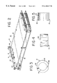
- FIG. 1 is a perspective exploded view of a preferred embodiment of an electromagnetic interference (EMI) shielding apparatus that is made in accordance with the invention
- FIG. 2 is an assembled view of the embodiment of FIG. 1;
- FIG. 3 is a front view of the compressible member of the embodiment of FIG. 1;
- FIG. 4 is a top view of the compressible member of FIG. 2;
- FIG. 5 is a side view of the compressible member of FIG. 2 with a portion broken away to show the foam body and the outer conductive portion.
- an electromagnetic interference (EMI) shielding apparatus 10 includes a circuit board assembly 12 and a compressible member 14 .
- the circuit board assembly 12 may preferably be any circuit board assembly that is slidably positioned in an electronic chassis (not shown) for high speed telecommunication and networking applications.
- the circuit board assembly 12 includes a bracket 16 and a circuit board 18 attached to the bracket 16 .
- a second circuit board 19 may also be attached to the bracket 16 .
- the bracket 16 serves as a faceplate for the circuit board assembly 12 .
- the size and shape of the bracket 16 may vary depending on the size and configuration of the circuit board 18 .
- the bracket 16 may preferably be any suitable rigid material such as, for example, metal.
- the bracket 16 includes an inner surface 20 and a flange portion 24 that extends along the length of the bracket 16 . As shown in FIG. 2, the bracket 16 may also preferably include a second flange portion 25 opposite flange portion 24 . Referring to FIG. 1, an opening 26 is formed in the bracket 16 to receive a connector 30 mounted on the circuit board 18 . A second opening 28 may preferably be formed in the bracket 16 to receive a second connector 32 . The number of openings in the bracket 16 may vary depending upon the number of connectors mounted in the circuit board 18 .
- the connector 30 is positioned on the circuit board 18 for insertion through the opening 26 in the bracket 16 .
- the connector 30 may preferably be surface mounted to the circuit board 18 .
- the circuit board 18 may preferably be any conventional printed circuit board.
- the connector 30 may preferably be any electronic connector such as, for example, a right-angled F-Series Connector.
- the compressible member 14 includes an outer conductive portion 34 .
- the compressible member 14 is positioned between the connector 30 and the inner surface 20 of the bracket 16 .
- the compressible member 14 is in contact with the connector 30 and the inner surface 20 of the bracket (see FIG. 2) to prevent electromagnetic emissions from exiting through the opening 26 in the bracket 16 .
- the compressible member 14 may preferably have a foam body 40 that is covered by the outer conductive portion 34 (see FIG. 5 ).
- the foam material may preferably be rated to comply with UL requirements, and in particular, UL1950.
- the outer conductive portion 34 of compressible member 14 may preferably be comprised of metalized fabric.
- the compressible member 14 may preferably compress between 5% to 60%. For the embodiment shown in FIGS. 1-2, the compressible member 14 has been found to provide maximum shielding effectiveness when compressed at least about 30%. The inherent flexibility of the compressible member 14 prevents excessive amounts of electromagnetic radiation from exiting the assembly 12 through gaps between components that are out of tolerance.
- the compressible member 14 includes an opening 15 formed therein for receiving the connector 30 .
- the outer conductive portion 34 of the compressible member 14 is in contact with the inner surface 20 of the bracket 16 .
- the outer conductive portion 34 of the compressible member 34 is also in contact with the flange portion 24 .
- the advantage of this arrangement is that the compressible member 14 provides continuous electrical grounding between the circuit board 18 and the bracket 16 .
- the bracket 16 is therefore grounded to the electronic chassis (not shown) when the circuit board assembly 12 is installed in the chassis.
- the outer conductive portion 34 of the compressible member 14 includes a first flat surface 36 and a second flat surface 38 .
- the first flat surface 36 is in contact with the flange portion 24
- the second flat surface is in contact with circuit board 18 .
- the flat surfaces ensure the electrical grounding between the circuit board 18 and the bracket 16 .
- the compressible member 14 is positioned between the connector 30 and an inner surface 20 of the bracket 16 .
- the compressible member 14 is positioned so that the stem portion 31 of the connector 30 is inserted through the opening 15 in the compressible member 14 .
- the bracket 16 is then positioned so that the stem portion 31 of the connector 30 is inserted through the opening 26 in the bracket 16 .
- the compressible member 14 is compressed between the connector 30 and the inner surface 20 of the bracket 16 .
- the compressible member 14 contacts the circuit board 18 and the flange portion 24 of the bracket 16 thereby electrically grounding the circuit board 18 to the bracket 16 .
- the circuit board 18 is then fastened to the bracket 16 .
Abstract
Description
Claims (12)
Priority Applications (1)
| Application Number | Priority Date | Filing Date | Title |
|---|---|---|---|
| US09/307,364 US6188017B1 (en) | 1999-05-07 | 1999-05-07 | Electromagnetic interference (EMI) shielding apparatus |
Applications Claiming Priority (1)
| Application Number | Priority Date | Filing Date | Title |
|---|---|---|---|
| US09/307,364 US6188017B1 (en) | 1999-05-07 | 1999-05-07 | Electromagnetic interference (EMI) shielding apparatus |
Publications (1)
| Publication Number | Publication Date |
|---|---|
| US6188017B1 true US6188017B1 (en) | 2001-02-13 |
Family
ID=23189427
Family Applications (1)
| Application Number | Title | Priority Date | Filing Date |
|---|---|---|---|
| US09/307,364 Expired - Fee Related US6188017B1 (en) | 1999-05-07 | 1999-05-07 | Electromagnetic interference (EMI) shielding apparatus |
Country Status (1)
| Country | Link |
|---|---|
| US (1) | US6188017B1 (en) |
Cited By (5)
| Publication number | Priority date | Publication date | Assignee | Title |
|---|---|---|---|---|
| US6552914B1 (en) * | 2000-03-27 | 2003-04-22 | Aten International Co., Ltd. | Circuit board assembly mechanism |
| US20050088832A1 (en) * | 2003-10-24 | 2005-04-28 | Po-Chang Su | ESD protection structure and device utilizing the same |
| US20060081389A1 (en) * | 2004-10-14 | 2006-04-20 | Pille James D | Aesthetically colored EMI shields |
| US20060080825A1 (en) * | 2004-10-14 | 2006-04-20 | Pille James D | Methods related to electromagnetic interference shielding |
| US20130044451A1 (en) * | 2011-08-19 | 2013-02-21 | Hon Hai Precision Industry Co., Ltd. | Electronic device with electromagnetic shielding function |
Citations (2)
| Publication number | Priority date | Publication date | Assignee | Title |
|---|---|---|---|---|
| US5317105A (en) * | 1992-12-18 | 1994-05-31 | Alcatel Network Systems, Inc. | EMI/RFI gasket apparatus |
| US5980275A (en) * | 1995-08-21 | 1999-11-09 | International Business Machines, Corp. | Electronic circuit board interface mounting bracket |
-
1999
- 1999-05-07 US US09/307,364 patent/US6188017B1/en not_active Expired - Fee Related
Patent Citations (2)
| Publication number | Priority date | Publication date | Assignee | Title |
|---|---|---|---|---|
| US5317105A (en) * | 1992-12-18 | 1994-05-31 | Alcatel Network Systems, Inc. | EMI/RFI gasket apparatus |
| US5980275A (en) * | 1995-08-21 | 1999-11-09 | International Business Machines, Corp. | Electronic circuit board interface mounting bracket |
Cited By (7)
| Publication number | Priority date | Publication date | Assignee | Title |
|---|---|---|---|---|
| US6552914B1 (en) * | 2000-03-27 | 2003-04-22 | Aten International Co., Ltd. | Circuit board assembly mechanism |
| US20050088832A1 (en) * | 2003-10-24 | 2005-04-28 | Po-Chang Su | ESD protection structure and device utilizing the same |
| US7088592B2 (en) * | 2003-10-24 | 2006-08-08 | Asustek Computer Inc. | ESD protection structure and device utilizing the same |
| US20060081389A1 (en) * | 2004-10-14 | 2006-04-20 | Pille James D | Aesthetically colored EMI shields |
| US20060080825A1 (en) * | 2004-10-14 | 2006-04-20 | Pille James D | Methods related to electromagnetic interference shielding |
| US20130044451A1 (en) * | 2011-08-19 | 2013-02-21 | Hon Hai Precision Industry Co., Ltd. | Electronic device with electromagnetic shielding function |
| US8537568B2 (en) * | 2011-08-19 | 2013-09-17 | Fu Tai Hua Industry (Shenzhen) Co., Ltd. | Electronic device with electromagnetic shielding function |
Similar Documents
| Publication | Publication Date | Title |
|---|---|---|
| US5769667A (en) | Low cost filtered and shielded electronic connector | |
| US5975953A (en) | EMI by-pass gasket for shielded connectors | |
| US5847938A (en) | Press-fit shields for electronic assemblies, and methods for assembling the same | |
| EP1187268B1 (en) | Coaxial connector module and method of fabricating same | |
| US5311408A (en) | Electronic assembly with improved grounding and EMI shielding | |
| EP1208618B1 (en) | Control device and soldering method | |
| US5899755A (en) | Integrated circuit test socket with enhanced noise imminity | |
| US5748449A (en) | Electrical enclosure for radio | |
| CN1152972A (en) | Assembly of shielded conenctors and a board having plated holes | |
| EP0661918A1 (en) | Electronic component enclosure for rf shielding | |
| US6140575A (en) | Shielded electronic circuit assembly | |
| US5823827A (en) | Low cost filtered and shielded electronic connector | |
| US5520554A (en) | Cable connection and shielding device | |
| US6188017B1 (en) | Electromagnetic interference (EMI) shielding apparatus | |
| US6203373B1 (en) | Shielded electrical connector | |
| US6235985B1 (en) | Low profile printed circuit board RF shield for radiating pin | |
| US5960136A (en) | Shielded fiber optic connector | |
| CA2038281C (en) | Crt with electromagnetic radiation reducing means | |
| US6335482B1 (en) | Cable screen connection method and cable grommet | |
| DE4212369C2 (en) | Control unit | |
| JP3313479B2 (en) | Cable with connector | |
| CN1127183C (en) | Shielded electric connector | |
| EP0984515B1 (en) | Shielded electrical connector | |
| EP1064702B1 (en) | Decoupled bnc connector | |
| JPH05114438A (en) | Shield structure of connector |
Legal Events
| Date | Code | Title | Description |
|---|---|---|---|
| AS | Assignment |
Owner name: 3COM CORP., ILLINOIS Free format text: ASSIGNMENT OF ASSIGNORS INTEREST;ASSIGNOR:AUGUST, JOSEPH M., JR.;REEL/FRAME:009948/0148 Effective date: 19990503 |
|
| AS | Assignment |
Owner name: UTSTARCOM, INC., CALIFORNIA Free format text: ASSIGNMENT OF PATENT RIGHTS;ASSIGNOR:3COM CORPORATION;REEL/FRAME:014499/0637 Effective date: 20030523 |
|
| FPAY | Fee payment |
Year of fee payment: 4 |
|
| FEPP | Fee payment procedure |
Free format text: PAYOR NUMBER ASSIGNED (ORIGINAL EVENT CODE: ASPN); ENTITY STATUS OF PATENT OWNER: LARGE ENTITY |
|
| FPAY | Fee payment |
Year of fee payment: 8 |
|
| REMI | Maintenance fee reminder mailed | ||
| LAPS | Lapse for failure to pay maintenance fees | ||
| LAPS | Lapse for failure to pay maintenance fees |
Free format text: PATENT EXPIRED FOR FAILURE TO PAY MAINTENANCE FEES (ORIGINAL EVENT CODE: EXP.); ENTITY STATUS OF PATENT OWNER: LARGE ENTITY |
|
| STCH | Information on status: patent discontinuation |
Free format text: PATENT EXPIRED DUE TO NONPAYMENT OF MAINTENANCE FEES UNDER 37 CFR 1.362 |
|
| FP | Lapsed due to failure to pay maintenance fee |
Effective date: 20130213 |