US6198392B1 - Communications system and method with A/D converter - Google Patents
Communications system and method with A/D converter Download PDFInfo
- Publication number
- US6198392B1 US6198392B1 US09/249,287 US24928799A US6198392B1 US 6198392 B1 US6198392 B1 US 6198392B1 US 24928799 A US24928799 A US 24928799A US 6198392 B1 US6198392 B1 US 6198392B1
- Authority
- US
- United States
- Prior art keywords
- analog
- input
- digital
- integrated circuit
- coupled
- Prior art date
- Legal status (The legal status is an assumption and is not a legal conclusion. Google has not performed a legal analysis and makes no representation as to the accuracy of the status listed.)
- Expired - Lifetime
Links
Images


Classifications
-
- G—PHYSICS
- G01—MEASURING; TESTING
- G01D—MEASURING NOT SPECIALLY ADAPTED FOR A SPECIFIC VARIABLE; ARRANGEMENTS FOR MEASURING TWO OR MORE VARIABLES NOT COVERED IN A SINGLE OTHER SUBCLASS; TARIFF METERING APPARATUS; MEASURING OR TESTING NOT OTHERWISE PROVIDED FOR
- G01D9/00—Recording measured values
- G01D9/005—Solid-state data loggers
-
- G—PHYSICS
- G06—COMPUTING; CALCULATING OR COUNTING
- G06K—GRAPHICAL DATA READING; PRESENTATION OF DATA; RECORD CARRIERS; HANDLING RECORD CARRIERS
- G06K17/00—Methods or arrangements for effecting co-operative working between equipments covered by two or more of main groups G06K1/00 - G06K15/00, e.g. automatic card files incorporating conveying and reading operations
-
- G—PHYSICS
- G06—COMPUTING; CALCULATING OR COUNTING
- G06K—GRAPHICAL DATA READING; PRESENTATION OF DATA; RECORD CARRIERS; HANDLING RECORD CARRIERS
- G06K19/00—Record carriers for use with machines and with at least a part designed to carry digital markings
- G06K19/06—Record carriers for use with machines and with at least a part designed to carry digital markings characterised by the kind of the digital marking, e.g. shape, nature, code
- G06K19/067—Record carriers with conductive marks, printed circuits or semiconductor circuit elements, e.g. credit or identity cards also with resonating or responding marks without active components
- G06K19/07—Record carriers with conductive marks, printed circuits or semiconductor circuit elements, e.g. credit or identity cards also with resonating or responding marks without active components with integrated circuit chips
- G06K19/0716—Record carriers with conductive marks, printed circuits or semiconductor circuit elements, e.g. credit or identity cards also with resonating or responding marks without active components with integrated circuit chips at least one of the integrated circuit chips comprising a sensor or an interface to a sensor
- G06K19/0717—Record carriers with conductive marks, printed circuits or semiconductor circuit elements, e.g. credit or identity cards also with resonating or responding marks without active components with integrated circuit chips at least one of the integrated circuit chips comprising a sensor or an interface to a sensor the sensor being capable of sensing environmental conditions such as temperature history or pressure
-
- G—PHYSICS
- G06—COMPUTING; CALCULATING OR COUNTING
- G06K—GRAPHICAL DATA READING; PRESENTATION OF DATA; RECORD CARRIERS; HANDLING RECORD CARRIERS
- G06K19/00—Record carriers for use with machines and with at least a part designed to carry digital markings
- G06K19/06—Record carriers for use with machines and with at least a part designed to carry digital markings characterised by the kind of the digital marking, e.g. shape, nature, code
- G06K19/067—Record carriers with conductive marks, printed circuits or semiconductor circuit elements, e.g. credit or identity cards also with resonating or responding marks without active components
- G06K19/07—Record carriers with conductive marks, printed circuits or semiconductor circuit elements, e.g. credit or identity cards also with resonating or responding marks without active components with integrated circuit chips
- G06K19/0723—Record carriers with conductive marks, printed circuits or semiconductor circuit elements, e.g. credit or identity cards also with resonating or responding marks without active components with integrated circuit chips the record carrier comprising an arrangement for non-contact communication, e.g. wireless communication circuits on transponder cards, non-contact smart cards or RFIDs
Definitions
- This invention relates to systems and methods for monitoring parameters and for remote data telemetry.
- the invention also relates to radio frequency identification devices.
- RFIDs radio frequency identification devices
- RFIDs Electronic identification devices, such as radio frequency identification devices (RFIDs)
- RFIDs are known in the art.
- RFID devices are typically used for inventory tracking.
- One way of tracking objects is with an electronic identification system.
- an identification device may be provided with a unique identification code in order to distinguish between a number of different devices.
- the devices are entirely passive (have no power supply), which results in a small and portable package.
- identification systems are only capable of operation over a relatively short range, limited by the size of a magnetic field used to supply power to the devices and to communicate with the devices.
- Another type of wireless electronic identification system is an active wireless electronic identification system. Attention is directed towards commonly assigned U.S. patent application Ser. No. 08/705,043, filed Aug. 29, 1996, and incorporated herein by reference, which describes such active systems in detail.
- One such system is sold by Micron Communications Inc., 3176 S. Denver Way, Boise, Id. 83705 under the trademark Microstamp Engine (TM).
- TM Microstamp Engine
- These systems include integrated circuit devices which include an active transponder and are intended to be affixed to an object to be monitored. The devices are capable of receiving and processing instructions transmitted by an interrogator. A device receives the instruction, if within range, then processes the instruction and transmits a response, if appropriate.
- the interrogation signal and the responsive signal are typically radio-frequency (RF) signals produced by an RF transmitter circuit.
- RF radio-frequency
- active transponder devices Because active devices have their own power sources, and do not need to be in close proximity to an interrogator or reader to receive power via magnetic coupling. Therefore, active transponder devices tend to be more suitable for applications requiring tracking of a tagged device that may not be in close proximity to an interrogator. For example, active transponder devices tend to be more suitable for inventory control or tracking.
- the Microstamp engine is capable of communications, it can be used for applications other than just inventory tracking and other typical RFID applications.
- the Microstamp engine includes an internal A/D converter used for battery voltage sensing, but that A/D converter does not have an external input.
- a disadvantage of an internal A/D converter is that the user does not have the opportunity to use an A/D converter with more resolution than the internal A/D converter should the user be willing to pay extra for such resolution. Additionally, during the service life of a Microstamp engine, A/D converters may become available with higher resolution than the internal A/D converter.
- the invention provides a wireless identification device configured to provide a signal to identify the device in response to an interrogation signal.
- the invention provides coupling an analog to digital converter to the wireless identification device.
- the invention also provides a communications system comprising a radio frequency identification device including an integrated circuit.
- the integrated circuit has a single die including a microprocessor, a receiver coupled to the microprocessor, and a backscatter transmitter coupled to the microprocessor.
- the integrated circuit also has a digital input.
- the receiver is configured to receive wireless communications from a remote interrogator.
- the communications system further includes an analog to digital converter external of the single die.
- the analog to digital converter has a digital output coupled to the digital input of the integrated circuit, and has an analog input configured to be coupled to an analog measuring device.
- the radio frequency identification device is configured to transmit a signal indicative of the analog input using the backscatter transmitter.
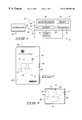
- FIG. 1 is a high level circuit schematic showing an interrogator and a radio frequency identification device embodying the invention.
- FIG. 2 is a front view of a housing, in the form of a badge or card, supporting the circuit of FIG. 1 according to one embodiment the invention.
- FIG. 3 is a front view of a housing supporting the circuit of FIG. 1 according to another embodiment of the invention.
- FIG. 4 is a circuit schematic of circuitry in accordance with one embodiment of the invention.
- FIG. 5 is a circuit schematic of circuitry added to the circuitry of FIG. 4 in an alternative embodiment of the invention.
- FIG. 1 illustrates a wireless identification device 10 in accordance with one embodiment of the invention.
- the wireless identification device is a radio frequency data communication device 10 , and includes RFID circuitry 12 .
- the device 10 further includes an antenna 14 connected to the circuitry 12 for wireless or radio frequency transmission by the circuitry 12 and an antenna 15 coupled to the circuitry 12 for wireless or radio frequency reception by the circuitry 12 .
- the antennas 14 and 15 are microstrip antennas.
- the RFID circuitry 12 is defined by an integrated circuit as described in the above-incorporated patent application Ser. No. 08/705,043, filed Aug. 29, 1996. Other embodiments are possible.
- a power source or supply 16 is connected to the integrated circuit 12 to supply power to the integrated circuit 12 .
- the power source 16 comprises a battery.
- the device 10 transmits and receives radio frequency communications to and from an interrogator 18 .
- An exemplary interrogator is described in commonly assigned U.S. patent application Ser. No. 08/907,689, filed Aug. 8, 1997 and incorporated herein by reference.
- the interrogator 18 includes an antenna 20 , as well as dedicated transmitting and receiving circuitry, complementary to that implemented on the integrated circuit 12 .
- the interrogator 18 transmits an interrogation signal or command 22 via the antenna 20 .
- the device 10 receives the incoming interrogation signal via antenna 15 .
- the device 10 responds by generating and transmitting a responsive signal or reply 24 via antenna 14 .
- the responsive signal 24 typically includes information that uniquely identifies, or labels the particular device 12 that is transmitting, so as to identify any object or person with which the device 12 is associated.
- FIG. 1 Although only one device 10 is shown in FIG. 1, typically there will be multiple devices 10 that correspond with the interrogator 18 , and the particular devices 10 that are in communication with the interrogator 18 will typically change over time. In the illustrated embodiment in FIG. 1, there is no communication between multiple devices 10 . Instead, the devices 10 respectively communicate with the interrogator 18 . Multiple devices 10 can be used in the same field of an interrogator 18 (i.e., within communications range of an interrogator 18 ).
- the device 10 can be included in any appropriate housing or packaging.
- Various methods of manufacturing housings are described in commonly assigned U.S. patent application Ser. No. 08/800,037, filed Feb. 13, 1997, and incorporated herein by reference.
- FIG. 2 shows but one embodiment in the form of a card or badge 26 including a housing 28 of plastic or other suitable material supporting the device 10 and the power supply 16 .
- a face of the badge 26 has visual identification features such as graphics, text, information found on identification or credit cards, etc.
- FIG. 3 illustrates but one alternative housing supporting the device 10 . More particularly, FIG. 3 shows a miniature housing 28 encasing the device 10 and power supply 16 to define a tag which can be supported by an object (e.g., hung from an object, affixed to an object, etc.). Although two particular types of housings have been disclosed, other forms of housings are employed in alternative embodiments.
- the battery 16 can take any suitable form.
- the battery type will be selected depending on weight, size, and life requirements for a particular application.
- the battery 16 is a thin profile button-type cell forming a small, thin energy cell more commonly utilized in watches and small electronic devices requiring a thin profile.
- a conventional button-type cell has a pair of electrodes, an anode formed by one face and a cathode formed by an opposite face.
- the power source 16 comprises a series connected pair of button type cells. In other alternative embodiments, other types of suitable power source are employed.
- the circuitry 12 provides a responsive signal to the interrogator 18 by radio frequency. More particularly, the circuitry 12 comprises an integrated circuit including a single die having a backscatter transmitter 30 , a receiver 32 , a memory 34 , and a microprocessor 36 coupled to the transmitter 30 , receiver 32 , and memory 34 (FIG. 1) as is described in U.S. patent application Ser. No. 08/705,043.
- the interrogator 18 communicates with the devices 10 via an electromagnetic link, such as via an RF link (e.g., at microwave frequencies, in one embodiment), so all transmissions by the interrogator 18 are heard simultaneously by all devices 10 within range.
- an electromagnetic link such as via an RF link (e.g., at microwave frequencies, in one embodiment)
- FIG. 4 illustrates a communications system 36 in accordance with one embodiment of the invention.
- the communications system 36 includes an analog to digital converter 38 coupled to the integrated circuit 12 .
- the analog to digital converter 38 is external of the single die integrated circuit 12 .
- the integrated circuit 12 has a digital input 40 .
- the analog to digital converter 38 has a digital output 42 coupled to the digital input 40 of the integrated circuit 12 .
- the analog to digital converter 38 has first and second analog inputs 44 and 46 coupled to an analog measuring device 48 such as a temperature sensor, water level sensor, pressure sensor, or any other sensor that produces a voltage.
- the analog to digital converter 38 provides at its digital output 42 a signal indicative of the difference between first and second voltages applied to the first and second analog inputs 44 and 46 .
- the communications system 36 further comprises transient voltage protection circuitry 50 coupled between the analog inputs 44 and 46 .
- the transient voltage protection circuitry 50 protects the analog inputs' maximum ratings from being exceeded. By using transient voltage protection circuitry 50 , the effects of ESD (Electro-Static Discharge), voltage transients, and induced electrical noise (from the use of lengthy wire connections) can be reduced, and circuit performance can be enhanced.
- ESD Electro-Static Discharge
- the integrated circuit 12 further has a clock output 51 , and the analog to digital converter 38 has a clock input 53 coupled to the clock output 51 .
- the analog to digital converter 38 further has a chip select input 54 which, when triggered, initiates an analog to digital conversion.
- the integrated circuit 12 further has a wakeup output 52 , coupled to the chip select input 54 .
- a signal is produced at the wakeup output 52 to trigger the chip select input 54 in response to the receiver 32 (of FIG. 1) receiving a wireless communication.
- the integrated circuit 12 In response to the receiver 32 (of FIG. 1) receiving a read digital input command from the interrogator 18 , the integrated circuit 12 (of FIG. 4) provides a signal at the wakeup output 52 and reads the digital input 40 .
- the analog to digital converter 38 transmits a signal indicative of the voltage differential at the analog inputs 44 and 46 , using the backscatter transmitter 30 (of FIG. 1 ), in response to a read digital port command by the interrogator 18 . More particularly, after the interrogator 18 transmits a read digital port command, the analog to digital converter initiates an analog to digital conversion of the difference in voltages at the analog inputs 44 and 46 . The digital conversion is read by the integrated circuit 12 and transmitted using the backscatter transmitter 30 .
- the analog to digital converter 38 has a voltage supply input 56 , a ground connector 57 , and a reference voltage input 59 .
- the communications system 36 further comprises a voltage regulator 58 coupled to the reference voltage input 59 and to the voltage supply input 56 .
- the voltage regulator 58 increases accuracy of the digital output by providing a stable voltage supply as well as decreased power consumption.
- the voltage regulator 58 is omitted.
- the integrated circuit 12 is a Microstamp Engine SOIC (TM) integrated circuit, part number MSEM256X10SG available from Micron Communications, 3176 S. Denver Way, Boise, Id. 83705, and has the following pin assignments (not shown): a pin 2 defines the wakeup output 52 ; a pin 18 defines the clock output 51 ; and a pin 17 defines the digital input 40 .
- TM Microstamp Engine SOIC
- the analog to digital converter 38 is an analog to digital converter integrated circuit, part number LTC1197 available from Linear Technology Corporation, and has the following pin assignments: a pin 1 defines the chip select input 54 ; a pin 2 defines the analog input 44 ; a pin 3 defines the analog input 46 ; a pin 4 defines the ground connector 57 ; a pin 5 defines the reference voltage input 59 ; a pin 6 defines the digital output 42 ; a pin 7 defines the clock input 53 ; and a pin 8 defines the voltage supply input 56 .
- Other analog to digital converters can be employed.
- the voltage regulator 58 is a Micropower Voltage Regulator (TM), part number MC78LC50 available from Motorola, and has the following pin assignments: a pin 1 defines a ground connector; a pin 2 defines an input 68 ; and a pin 3 defines an output 70 (FIG. 4 ). As shown in FIG. 4, a capacitor 72 is coupled between the input 68 and ground; and a capacitor 74 is coupled between the output 70 and ground. In the illustrated embodiment, the capacitors 72 and 74 respectively have values of 0.1 ⁇ F.
- the input 68 is coupled to a voltage supply 76 and a pull-up resistor 78 is coupled between the voltage supply 76 and the wakeup output 52 .
- the resistor 78 has a value of 100 k ⁇ .
- a resistor 80 is shown coupled between the digital output 42 and digital input 40 .
- the resistor 80 has a value of 10 k ⁇ .
- the transient voltage suppressor 50 is a Transorb (TM) surge suppressor.
- the communications system 36 further includes a binary counter 62 coupled between the wakeup output 52 and the chip select input 54 .
- the binary counter 62 causes the integrated circuit 12 to receive from the analog to digital converter 38 multiple conversions from analog to digital per trigger signal.
- the binary counter 62 is omitted and the wakeup output 52 is coupled to the chip select input 54 .
- the binary counter 62 shown in FIG. 5 includes an integrated circuit 80 .
- the integrated circuit 80 includes a load input 82 and a VCC voltage supply input 84 coupled to the voltage supply 76 , enable T and enable P inputs 86 and 88 (only one is used, however they are tied together so there is no pin which is floating), a clear input 90 , a clock input 92 coupled to the clock output 51 , a ground terminal 94 coupled to ground, and a ripple carry output 96 .
- the integrated circuit 80 is a synchronous binary counter with asynchronous clear, part number MM74HC161 available from National Semiconductor, and has the following pin assignments: a pin 1 defines the clear input 90 ; a pin 2 defines the clock input 92 ; a pin 7 defines the enable P input 88 ; a pin 8 defines the ground input 94 ; a pin 9 defines the load input 82 ; a pin 10 defines the enable T input 86 ; a pin 15 defines the ripple carry output 96 , and a pin 16 defines the voltage supply input 84 .
- Other integrated circuits could be employed.
- the binary counter 62 further includes a NAND gate 98 having inputs 100 and 101 both coupled to the wakeup output 52 and having an output 102 coupled to the enable T input 86 , the enable p input 88 , and the clear input 90 .
- the binary counter 62 further includes a NAND gate 104 having inputs 106 and 108 both coupled to the ripple carry output 96 and having an output 110 .
- the binary counter 62 further includes a NAND gate 112 having an input 114 coupled to the output 110 of the NAND gate 104 , having an input 116 coupled to the output 102 of the NAND gate 98 , and having an output 118 coupled to the input 54 of the analog to digital converter 38 .
- the clock output 51 is also coupled to the clock input 53 of the analog to digital converter 38 of FIG. 4 as it would be if the binary counter 62 were omitted. Also, if the binary counter 62 were omitted, the wakeup output 52 would be coupled directly to the chip select input 54 of the analog to digital converter 38 .
- an integrated circuit having four NAND gates is used to define the NAND gates 98 , 104 , and 112 .
- the integrated circuit used to define the NAND gates 98 , 104 , and 112 is a MM74HC00 integrated circuit available from National Semiconductor.
- the binary counter 62 By using the binary counter 62 , thirty-two conversions from analog to digital are possible per RF command from the interrogator to read the digital port of the integrated circuit 12 . Otherwise, there would only be one sample per RF command. With the thirty-two samples, averaging can be performed to obtain a more accurate reading. In the illustrated embodiment, every two bytes read by the integrated circuit 12 initiates a conversion stroke from analog to digital. With the binary counter 62 , sixty-four bytes are available, resulting in thirty-two conversions.
- the method comprises supporting the monolithic semiconductor integrated circuit 12 from a substrate.
- the substrate can be a circuit board or other sheet capable of supporting integrated circuits thereon.
- the substrate comprises a plastic sheet 66 that makes up a portion of the housing 28 .
- Alternative substrates are possible (FIG. 2 ).
- the microstrip antenna 15 (of FIG. 2) is supported from the substrate 66 , external of the integrated circuit 12 , and the microstrip antenna 15 is electrically coupled to the receiver 32 .
- printed thick film is printed on the substrate to define the antenna 15 and intersects a pin on the integrated circuit 12 for electrical coupling to the receiver 32 .
- the microstrip antenna 14 is supported from the substrate 66 , external of the integrated circuit 12 , and the microstrip antenna 14 is electrically coupled to the transmitter 30 .
- printed thick film is printed on the substrate to define the antenna 15 and intersects a pin on the integrated circuit 12 for electrical coupling to the receiver 32 as described in commonly assigned U.S. patent application Ser. No. 08/800,037, filed Feb. 13, 1997.
- the battery 16 is supported from the substrate, and electrically coupled to the integrated circuit 12 to supply operating power to the integrated circuit 12 .
- the analog to digital converter 38 is coupled to the integrated circuit 12 .
- the analog to digital converter 38 is coupled to the integrated circuit 12
- the battery 16 is coupled to the integrated circuit substantially at the same time by mounting the analog to digital converter 38 , battery 16 , and integrated circuit 12 onto traces (e.g., printed thick film in one embodiment) drawn on the substrate 66 or circuit board. Assembly can take place in a manner similar to that disclosed in commonly assigned U.S. patent application Ser. No. 08/800,037, filed Feb. 13, 1997.
- a digital signal indicative of the difference in magnitudes of the voltages at the analog inputs 44 and 46 is transmitted from the integrated circuit 12 to the interrogator 18 using the backscatter transmitter 30 .
- a communications system where measurements from analog devices can be transmitted over a range longer than is possible with magnetic coupling by using an integrated circuit having a microprocessor, receiver, memory, and backscatter transmitter.
Abstract
Description
Claims (35)
Priority Applications (4)
| Application Number | Priority Date | Filing Date | Title |
|---|---|---|---|
| US09/249,287 US6198392B1 (en) | 1999-02-10 | 1999-02-10 | Communications system and method with A/D converter |
| US09/765,235 US6831561B2 (en) | 1999-02-10 | 2001-01-16 | Communications system and method with A/D converter |
| US10/893,112 US7327263B2 (en) | 1999-02-10 | 2004-07-16 | Communications system and method with A/D converter |
| US11/855,788 US7994922B2 (en) | 1999-02-10 | 2007-09-14 | Communications system and method with A/D converter |
Applications Claiming Priority (1)
| Application Number | Priority Date | Filing Date | Title |
|---|---|---|---|
| US09/249,287 US6198392B1 (en) | 1999-02-10 | 1999-02-10 | Communications system and method with A/D converter |
Related Child Applications (1)
| Application Number | Title | Priority Date | Filing Date |
|---|---|---|---|
| US09/765,235 Continuation US6831561B2 (en) | 1999-02-10 | 2001-01-16 | Communications system and method with A/D converter |
Publications (1)
| Publication Number | Publication Date |
|---|---|
| US6198392B1 true US6198392B1 (en) | 2001-03-06 |
Family
ID=22942828
Family Applications (4)
| Application Number | Title | Priority Date | Filing Date |
|---|---|---|---|
| US09/249,287 Expired - Lifetime US6198392B1 (en) | 1999-02-10 | 1999-02-10 | Communications system and method with A/D converter |
| US09/765,235 Expired - Fee Related US6831561B2 (en) | 1999-02-10 | 2001-01-16 | Communications system and method with A/D converter |
| US10/893,112 Expired - Fee Related US7327263B2 (en) | 1999-02-10 | 2004-07-16 | Communications system and method with A/D converter |
| US11/855,788 Expired - Fee Related US7994922B2 (en) | 1999-02-10 | 2007-09-14 | Communications system and method with A/D converter |
Family Applications After (3)
| Application Number | Title | Priority Date | Filing Date |
|---|---|---|---|
| US09/765,235 Expired - Fee Related US6831561B2 (en) | 1999-02-10 | 2001-01-16 | Communications system and method with A/D converter |
| US10/893,112 Expired - Fee Related US7327263B2 (en) | 1999-02-10 | 2004-07-16 | Communications system and method with A/D converter |
| US11/855,788 Expired - Fee Related US7994922B2 (en) | 1999-02-10 | 2007-09-14 | Communications system and method with A/D converter |
Country Status (1)
| Country | Link |
|---|---|
| US (4) | US6198392B1 (en) |
Cited By (55)
| Publication number | Priority date | Publication date | Assignee | Title |
|---|---|---|---|---|
| US20010001553A1 (en) * | 1999-02-10 | 2001-05-24 | Scott Hahn | Communications system and method with A/D converter |
| US6411075B1 (en) * | 1999-03-18 | 2002-06-25 | Nanosurf Ag | Electronic frequency measuring device and its use |
| US6466130B2 (en) | 1999-07-29 | 2002-10-15 | Micron Technology, Inc. | Wireless communication devices, wireless communication systems, communication methods, methods of forming radio frequency identification devices, methods of testing wireless communication operations, radio frequency identification devices, and methods of forming radio frequency identification devices |
| US6630885B2 (en) | 2000-07-26 | 2003-10-07 | Bridgestone/Firestone North American Tire, Llc | Electronic tire management system |
| US6657477B2 (en) * | 2001-05-04 | 2003-12-02 | Koninklijke Philips Electronics N.V. | Integrated circuit |
| US20040130016A1 (en) * | 2002-09-06 | 2004-07-08 | Hitoshi Yamamoto | Semiconductor device and different levels of signal processing systems using the same |
| US20040198233A1 (en) * | 2002-10-02 | 2004-10-07 | Pratt Richard M. | Radio frequency identification devices, backscatter communication device wake-up methods, communication device wake-up methods and a radio frequency identification device wake-up method |
| US6837427B2 (en) | 2001-11-21 | 2005-01-04 | Goliath Solutions, Llc. | Advertising compliance monitoring system |
| US20050006466A1 (en) * | 2001-11-21 | 2005-01-13 | Overhultz Gary L. | Advertising compliance monitoring system |
| US20050012612A1 (en) * | 2000-04-21 | 2005-01-20 | Usm Systems, Ltd. | Event driven information system |
| US20050039949A1 (en) * | 1999-08-27 | 2005-02-24 | Lex Kosowsky | Methods for fabricating current-carrying structures using voltage switchable dielectric materials |
| US20050083201A1 (en) * | 1999-07-29 | 2005-04-21 | Trosper Scott T. | Radio frequency identification devices, remote communication devices, identification systems, communication methods, and identification methods |
| US20070114640A1 (en) * | 2005-11-22 | 2007-05-24 | Shocking Technologies, Inc. | Semiconductor devices including voltage switchable materials for over-voltage protection |
| US20070126018A1 (en) * | 2005-11-22 | 2007-06-07 | Lex Kosowsky | Light-emitting device using voltage switchable dielectric material |
| US7310070B1 (en) | 2006-08-23 | 2007-12-18 | Goliath Solutions, Llc | Radio frequency identification shelf antenna with a distributed pattern for localized tag detection |
| US20080023675A1 (en) * | 1999-08-27 | 2008-01-31 | Lex Kosowsky | Device applications for voltage switchable dielectric material having high aspect ratio particles |
| US20080032049A1 (en) * | 2006-07-29 | 2008-02-07 | Lex Kosowsky | Voltage switchable dielectric material having high aspect ratio particles |
| US20080035370A1 (en) * | 1999-08-27 | 2008-02-14 | Lex Kosowsky | Device applications for voltage switchable dielectric material having conductive or semi-conductive organic material |
| US20080111675A1 (en) * | 2006-11-10 | 2008-05-15 | Micron Technology, Inc. | Tracking systems, passive RFIDs, methods of locating and identifying RFIDs, and methods of tracking items |
| US7374096B2 (en) | 2001-11-21 | 2008-05-20 | Goliath Solutions, Llc | Advertising compliance monitoring system |
| US20080186178A1 (en) * | 2007-02-07 | 2008-08-07 | Micron Technology, Inc. | RFIDS, interrogators, indication systems, methods of determining a bi-directional communication range of an interrogator, methods of activating an observable indicator, and methods of indicating bi-directional functionality of a radio connection |
| US20080313576A1 (en) * | 2007-06-13 | 2008-12-18 | Lex Kosowsky | System and method for including protective voltage switchable dielectric material in the design or simulation of substrate devices |
| WO2007062170A3 (en) * | 2005-11-22 | 2009-04-30 | Shocking Technologies Inc | Wireless communication device using voltage switchable dielectric material |
| US20090212266A1 (en) * | 2008-01-18 | 2009-08-27 | Lex Kosowsky | Voltage switchable dielectric material having bonded particle constituents |
| US20090242855A1 (en) * | 2006-11-21 | 2009-10-01 | Robert Fleming | Voltage switchable dielectric materials with low band gap polymer binder or composite |
| US20090256669A1 (en) * | 2008-04-14 | 2009-10-15 | Lex Kosowsky | Substrate device or package using embedded layer of voltage switchable dielectric material in a vertical switching configuration |
| US20090315683A1 (en) * | 2008-06-24 | 2009-12-24 | Keystone Technology Solutions, Llc | Analog RFID System |
| US20100044080A1 (en) * | 1999-08-27 | 2010-02-25 | Lex Kosowsky | Metal Deposition |
| US20100044079A1 (en) * | 1999-08-27 | 2010-02-25 | Lex Kosowsky | Metal Deposition |
| US20100047535A1 (en) * | 2008-08-22 | 2010-02-25 | Lex Kosowsky | Core layer structure having voltage switchable dielectric material |
| US20100065785A1 (en) * | 2008-09-17 | 2010-03-18 | Lex Kosowsky | Voltage switchable dielectric material containing boron compound |
| US20100090176A1 (en) * | 2008-09-30 | 2010-04-15 | Lex Kosowsky | Voltage Switchable Dielectric Material Containing Conductor-On-Conductor Core Shelled Particles |
| US20100090178A1 (en) * | 2008-09-30 | 2010-04-15 | Lex Kosowsky | Voltage switchable dielectric material containing conductive core shelled particles |
| US20100109834A1 (en) * | 2008-11-05 | 2010-05-06 | Lex Kosowsky | Geometric and electric field considerations for including transient protective material in substrate devices |
| US20100141376A1 (en) * | 2006-07-29 | 2010-06-10 | Lex Kosowsky | Electronic device for voltage switchable dielectric material having high aspect ratio particles |
| US20100155671A1 (en) * | 2006-07-29 | 2010-06-24 | Lex Kosowsky | Method for creating voltage switchable dielectric material |
| US20100264225A1 (en) * | 2005-11-22 | 2010-10-21 | Lex Kosowsky | Wireless communication device using voltage switchable dielectric material |
| US20100270588A1 (en) * | 2006-09-24 | 2010-10-28 | Shocking Technologies, Inc. | Formulations for voltage switchable dielectric material having a stepped voltage response and methods for making the same |
| US20110058291A1 (en) * | 2009-09-09 | 2011-03-10 | Lex Kosowsky | Geometric configuration or alignment of protective material in a gap structure for electrical devices |
| US20110061230A1 (en) * | 1999-08-27 | 2011-03-17 | Lex Kosowsky | Methods for Fabricating Current-Carrying Structures Using Voltage Switchable Dielectric Materials |
| US20110198544A1 (en) * | 2010-02-18 | 2011-08-18 | Lex Kosowsky | EMI Voltage Switchable Dielectric Materials Having Nanophase Materials |
| US20110211319A1 (en) * | 2010-02-26 | 2011-09-01 | Lex Kosowsky | Electric discharge protection for surface mounted and embedded components |
| US20110211289A1 (en) * | 2010-02-26 | 2011-09-01 | Lex Kosowsky | Embedded protection against spurious electrical events |
| US8151127B2 (en) | 2000-07-26 | 2012-04-03 | Bridgestone Americas Tire Operations, Llc | System for conserving battery life in a battery operated device |
| US8266465B2 (en) | 2000-07-26 | 2012-09-11 | Bridgestone Americas Tire Operation, LLC | System for conserving battery life in a battery operated device |
| US8272123B2 (en) | 2009-01-27 | 2012-09-25 | Shocking Technologies, Inc. | Substrates having voltage switchable dielectric materials |
| US8399773B2 (en) | 2009-01-27 | 2013-03-19 | Shocking Technologies, Inc. | Substrates having voltage switchable dielectric materials |
| CN101507129B (en) * | 2005-11-22 | 2013-03-27 | 肖克科技有限公司 | Wireless communication device using voltage switchable dielectric material |
| WO2013101538A1 (en) * | 2011-12-27 | 2013-07-04 | The Gillette Company | Apparatus and method for providing product information |
| FR2990314A1 (en) * | 2012-05-03 | 2013-11-08 | Commissariat Energie Atomique | MICROELECTRONIC DEVICE FOR WIRELESS TRANSMISSION |
| US8968606B2 (en) | 2009-03-26 | 2015-03-03 | Littelfuse, Inc. | Components having voltage switchable dielectric materials |
| US9082622B2 (en) | 2010-02-26 | 2015-07-14 | Littelfuse, Inc. | Circuit elements comprising ferroic materials |
| US9226391B2 (en) | 2009-01-27 | 2015-12-29 | Littelfuse, Inc. | Substrates having voltage switchable dielectric materials |
| CN105303207A (en) * | 2015-10-26 | 2016-02-03 | 太原理工大学 | Label communication system based on analog-to-digital conversion backscattering |
| RU2601183C1 (en) * | 2012-09-14 | 2016-10-27 | Дзе Жиллетт Компани | Radio frequency identification transponder containing sensor |
Families Citing this family (7)
| Publication number | Priority date | Publication date | Assignee | Title |
|---|---|---|---|---|
| WO2005050960A1 (en) * | 2003-11-15 | 2005-06-02 | Cingular Wireless Ii, Llc | Method, system, and apparatus for providing wireless identification to standard telephone |
| US20070057773A1 (en) * | 2005-09-09 | 2007-03-15 | Beedar Technology Inc. | Apparatus and Methods of Universal Radio Frequency Identification Sensing System |
| US20070093200A1 (en) * | 2005-10-21 | 2007-04-26 | Delphi Technologies, Inc. | Communications device for communicating between a vehicle and a call center |
| WO2008004205A1 (en) * | 2006-07-05 | 2008-01-10 | Elcam Medical Agricultural Cooperative Association Ltd. | Wireless medical monitoring system |
| NL1036710C2 (en) * | 2009-03-13 | 2010-09-14 | Lely Patent Nv | AGRICULTURE INFORMATION TAG. |
| FR3000587B1 (en) * | 2012-12-27 | 2016-04-15 | Commissariat Energie Atomique | DEVICE FOR DETECTING THE FLIGHT OF AN OBJECT |
| CN110085004B (en) * | 2019-05-09 | 2020-12-25 | 王亮 | Combustible gas detection alarm self-starting fan control system |
Citations (3)
| Publication number | Priority date | Publication date | Assignee | Title |
|---|---|---|---|---|
| US5446447A (en) * | 1994-02-16 | 1995-08-29 | Motorola, Inc. | RF tagging system including RF tags with variable frequency resonant circuits |
| US6075973A (en) * | 1998-05-18 | 2000-06-13 | Micron Technology, Inc. | Method of communications in a backscatter system, interrogator, and backscatter communications system |
| US6137422A (en) * | 1999-05-21 | 2000-10-24 | Micron Technology, Inc. | Communications system and method with D/A converter |
Family Cites Families (13)
| Publication number | Priority date | Publication date | Assignee | Title |
|---|---|---|---|---|
| US5019815A (en) * | 1979-10-12 | 1991-05-28 | Lemelson Jerome H | Radio frequency controlled interrogator-responder system with passive code generator |
| US4619002A (en) * | 1984-07-02 | 1986-10-21 | Motorola, Inc. | Self-calibrating signal strength detector |
| US5184349A (en) * | 1991-01-16 | 1993-02-02 | Motorola, Inc. | Amplitude control of a burst signal in a receiver |
| US6087930A (en) * | 1994-02-22 | 2000-07-11 | Computer Methods Corporation | Active integrated circuit transponder and sensor apparatus for transmitting vehicle tire parameter data |
| US6333690B1 (en) * | 1995-03-29 | 2001-12-25 | Medical Tracking Systems | Wide area multipurpose tracking system |
| US6130602A (en) * | 1996-05-13 | 2000-10-10 | Micron Technology, Inc. | Radio frequency data communications device |
| US6107910A (en) * | 1996-11-29 | 2000-08-22 | X-Cyte, Inc. | Dual mode transmitter/receiver and decoder for RF transponder tags |
| US6289209B1 (en) * | 1996-12-18 | 2001-09-11 | Micron Technology, Inc. | Wireless communication system, radio frequency communications system, wireless communications method, radio frequency communications method |
| US6084530A (en) * | 1996-12-30 | 2000-07-04 | Lucent Technologies Inc. | Modulated backscatter sensor system |
| US5952922A (en) * | 1996-12-31 | 1999-09-14 | Lucent Technologies Inc. | In-building modulated backscatter system |
| US5988510A (en) * | 1997-02-13 | 1999-11-23 | Micron Communications, Inc. | Tamper resistant smart card and method of protecting data in a smart card |
| US6046676A (en) * | 1997-11-14 | 2000-04-04 | International Business Machines Corporation | Self powered electronic memory identification tag with dual communication ports |
| US6198392B1 (en) * | 1999-02-10 | 2001-03-06 | Micron Technology, Inc. | Communications system and method with A/D converter |
-
1999
- 1999-02-10 US US09/249,287 patent/US6198392B1/en not_active Expired - Lifetime
-
2001
- 2001-01-16 US US09/765,235 patent/US6831561B2/en not_active Expired - Fee Related
-
2004
- 2004-07-16 US US10/893,112 patent/US7327263B2/en not_active Expired - Fee Related
-
2007
- 2007-09-14 US US11/855,788 patent/US7994922B2/en not_active Expired - Fee Related
Patent Citations (3)
| Publication number | Priority date | Publication date | Assignee | Title |
|---|---|---|---|---|
| US5446447A (en) * | 1994-02-16 | 1995-08-29 | Motorola, Inc. | RF tagging system including RF tags with variable frequency resonant circuits |
| US6075973A (en) * | 1998-05-18 | 2000-06-13 | Micron Technology, Inc. | Method of communications in a backscatter system, interrogator, and backscatter communications system |
| US6137422A (en) * | 1999-05-21 | 2000-10-24 | Micron Technology, Inc. | Communications system and method with D/A converter |
Non-Patent Citations (7)
| Title |
|---|
| "New Active RFID System Senses Temperature, Reads from 30 Meters," Automatic ID News, (Mar., 1999). |
| Linear Technology Data Sheets: LTC 1197/LTC 1197/LTC 1199L, pp. 1 and 2. |
| Micron Communications, Inc. Data Sheets: "MicroStamp Engine SOIC", pp. 1 and 2, Feb. 20, 1998. |
| Motorola, Inc. Data Sheets: "Micropower Voltage Regulator", pp. 1 and 2, 1997. |
| National Semiconductor Data Sheet: "MM54HC00/MM74HC00 Quad 2-Input NAND Gate", p. 3-3. |
| National Semiconductor Data Sheets: "MM54HC160/ MM74HC160 Synchronous Decade Counter with Asynchronous Clear . . . ", pp. 3-142 and 3-143. |
| Steve MacNaull, "Identec Web Pages," High-Tech, Safe Food Delivery, (Mar. 11, 1999). |
Cited By (116)
| Publication number | Priority date | Publication date | Assignee | Title |
|---|---|---|---|---|
| US6831561B2 (en) * | 1999-02-10 | 2004-12-14 | Micron Technology, Inc. | Communications system and method with A/D converter |
| US20010001553A1 (en) * | 1999-02-10 | 2001-05-24 | Scott Hahn | Communications system and method with A/D converter |
| US7994922B2 (en) | 1999-02-10 | 2011-08-09 | Round Rock Research, Llc | Communications system and method with A/D converter |
| US20080048866A1 (en) * | 1999-02-10 | 2008-02-28 | Scott Hahn | Communications System and Method with A/D Converter |
| US7327263B2 (en) | 1999-02-10 | 2008-02-05 | Micron Technology, Inc. | Communications system and method with A/D converter |
| US20050078007A1 (en) * | 1999-02-10 | 2005-04-14 | Scott Hahn | Communications system and method with A/D converter |
| US6411075B1 (en) * | 1999-03-18 | 2002-06-25 | Nanosurf Ag | Electronic frequency measuring device and its use |
| US20100013637A1 (en) * | 1999-07-29 | 2010-01-21 | Keystone Technology Solutions, Llc | Radio Frequency Identification Devices, Remote Communication Devices, Identification Systems, Communication Methods, and Identification Methods |
| US7071824B2 (en) * | 1999-07-29 | 2006-07-04 | Micron Technology, Inc. | Radio frequency identification devices, remote communication devices, identification systems, communication methods, and identification methods |
| US6466130B2 (en) | 1999-07-29 | 2002-10-15 | Micron Technology, Inc. | Wireless communication devices, wireless communication systems, communication methods, methods of forming radio frequency identification devices, methods of testing wireless communication operations, radio frequency identification devices, and methods of forming radio frequency identification devices |
| US7737851B2 (en) | 1999-07-29 | 2010-06-15 | Round Rock Research, Llc | Radio frequency identification devices, remote communication devices, identification systems, communication methods, and identification methods |
| US6545605B2 (en) | 1999-07-29 | 2003-04-08 | Micron Technology, Inc. | Methods of determining a communications range of an interrogator of a wireless identification system and methods of verifying operation of a wireless identification system |
| US8004407B2 (en) | 1999-07-29 | 2011-08-23 | Round Rock Research, Llc | Radio frequency identification devices, remote communication devices, identification systems, communication methods, and identification methods |
| US8253565B2 (en) | 1999-07-29 | 2012-08-28 | Round Rock Research, Llc | Radio frequency identification devices, remote communication devices, identification systems, communication methods, and identification methods |
| US20050083201A1 (en) * | 1999-07-29 | 2005-04-21 | Trosper Scott T. | Radio frequency identification devices, remote communication devices, identification systems, communication methods, and identification methods |
| US7518515B2 (en) | 1999-07-29 | 2009-04-14 | Keystone Technology Solutions, Llc | Method and system for RFID communication |
| US8487766B2 (en) | 1999-07-29 | 2013-07-16 | Round Rock Research, LLP | Radio frequency identification devices, remote communication devices, identification systems, communication methods, and identification methods |
| US20070035395A1 (en) * | 1999-07-29 | 2007-02-15 | Trosper Scott T | Wireless communication devices, radio frequency identification devices, radio frequency identification device communication systems, wireless communication methods, and radio frequency identification device communication methods |
| US7123148B2 (en) | 1999-07-29 | 2006-10-17 | Micron Technology, Inc. | Wireless communication devices, radio frequency identification devices, radio frequency identification device communication systems, wireless communication methods, and radio frequency identification device communication methods |
| US20100044079A1 (en) * | 1999-08-27 | 2010-02-25 | Lex Kosowsky | Metal Deposition |
| US20080035370A1 (en) * | 1999-08-27 | 2008-02-14 | Lex Kosowsky | Device applications for voltage switchable dielectric material having conductive or semi-conductive organic material |
| US20100044080A1 (en) * | 1999-08-27 | 2010-02-25 | Lex Kosowsky | Metal Deposition |
| US20050039949A1 (en) * | 1999-08-27 | 2005-02-24 | Lex Kosowsky | Methods for fabricating current-carrying structures using voltage switchable dielectric materials |
| US8117743B2 (en) | 1999-08-27 | 2012-02-21 | Shocking Technologies, Inc. | Methods for fabricating current-carrying structures using voltage switchable dielectric materials |
| US7695644B2 (en) | 1999-08-27 | 2010-04-13 | Shocking Technologies, Inc. | Device applications for voltage switchable dielectric material having high aspect ratio particles |
| US9144151B2 (en) | 1999-08-27 | 2015-09-22 | Littelfuse, Inc. | Current-carrying structures fabricated using voltage switchable dielectric materials |
| US20080023675A1 (en) * | 1999-08-27 | 2008-01-31 | Lex Kosowsky | Device applications for voltage switchable dielectric material having high aspect ratio particles |
| US7446030B2 (en) | 1999-08-27 | 2008-11-04 | Shocking Technologies, Inc. | Methods for fabricating current-carrying structures using voltage switchable dielectric materials |
| US20110061230A1 (en) * | 1999-08-27 | 2011-03-17 | Lex Kosowsky | Methods for Fabricating Current-Carrying Structures Using Voltage Switchable Dielectric Materials |
| US7026937B2 (en) | 2000-04-21 | 2006-04-11 | Usm Systems, Ltd. | Event driven information system |
| US20050012612A1 (en) * | 2000-04-21 | 2005-01-20 | Usm Systems, Ltd. | Event driven information system |
| US8151127B2 (en) | 2000-07-26 | 2012-04-03 | Bridgestone Americas Tire Operations, Llc | System for conserving battery life in a battery operated device |
| US6630885B2 (en) | 2000-07-26 | 2003-10-07 | Bridgestone/Firestone North American Tire, Llc | Electronic tire management system |
| US8266465B2 (en) | 2000-07-26 | 2012-09-11 | Bridgestone Americas Tire Operation, LLC | System for conserving battery life in a battery operated device |
| US6657477B2 (en) * | 2001-05-04 | 2003-12-02 | Koninklijke Philips Electronics N.V. | Integrated circuit |
| US7374096B2 (en) | 2001-11-21 | 2008-05-20 | Goliath Solutions, Llc | Advertising compliance monitoring system |
| US20080197193A1 (en) * | 2001-11-21 | 2008-08-21 | Overhultz Gary L | Advertising Compliance Monitoring System |
| US6951305B2 (en) | 2001-11-21 | 2005-10-04 | Goliath Solutions, Llc. | Advertising compliance monitoring system |
| US20050095573A1 (en) * | 2001-11-21 | 2005-05-05 | Overhultz Gary L. | Advertising compliance monitoring system |
| US7549579B2 (en) | 2001-11-21 | 2009-06-23 | Goliath Solutions, Llc | Advertising compliance monitoring system |
| US20050006466A1 (en) * | 2001-11-21 | 2005-01-13 | Overhultz Gary L. | Advertising compliance monitoring system |
| US6837427B2 (en) | 2001-11-21 | 2005-01-04 | Goliath Solutions, Llc. | Advertising compliance monitoring system |
| US7021535B2 (en) | 2001-11-21 | 2006-04-04 | Goliath Solutions, Llc | Advertising compliance monitoring system |
| US20040130016A1 (en) * | 2002-09-06 | 2004-07-08 | Hitoshi Yamamoto | Semiconductor device and different levels of signal processing systems using the same |
| US7224053B2 (en) * | 2002-09-06 | 2007-05-29 | Ricoh Company, Ltd. | Semiconductor device responsive to different levels of input and output signals and signal processing system using the same |
| US20040198233A1 (en) * | 2002-10-02 | 2004-10-07 | Pratt Richard M. | Radio frequency identification devices, backscatter communication device wake-up methods, communication device wake-up methods and a radio frequency identification device wake-up method |
| US20060100001A1 (en) * | 2002-10-02 | 2006-05-11 | Pratt Richard M | Backscatter communication device wake-up methods, communication device wake-up methods, and radio frequency identification device wake-up methods |
| US7019617B2 (en) | 2002-10-02 | 2006-03-28 | Battelle Memorial Institute | Radio frequency identification devices, backscatter communication device wake-up methods, communication device wake-up methods and a radio frequency identification device wake-up method |
| WO2007062170A3 (en) * | 2005-11-22 | 2009-04-30 | Shocking Technologies Inc | Wireless communication device using voltage switchable dielectric material |
| US20100264225A1 (en) * | 2005-11-22 | 2010-10-21 | Lex Kosowsky | Wireless communication device using voltage switchable dielectric material |
| US7923844B2 (en) | 2005-11-22 | 2011-04-12 | Shocking Technologies, Inc. | Semiconductor devices including voltage switchable materials for over-voltage protection |
| US8310064B2 (en) | 2005-11-22 | 2012-11-13 | Shocking Technologies, Inc. | Semiconductor devices including voltage switchable materials for over-voltage protection |
| CN101507129B (en) * | 2005-11-22 | 2013-03-27 | 肖克科技有限公司 | Wireless communication device using voltage switchable dielectric material |
| US7825491B2 (en) | 2005-11-22 | 2010-11-02 | Shocking Technologies, Inc. | Light-emitting device using voltage switchable dielectric material |
| US20100270545A1 (en) * | 2005-11-22 | 2010-10-28 | Lex Kosowsky | Light-emitting device using voltage switchable dielectric material |
| US20100270546A1 (en) * | 2005-11-22 | 2010-10-28 | Lex Kosowsky | Light-emitting device using voltage switchable dielectric material |
| US20100263200A1 (en) * | 2005-11-22 | 2010-10-21 | Lex Kosowsky | Wireless communication device using voltage switchable dielectric material |
| US20070126018A1 (en) * | 2005-11-22 | 2007-06-07 | Lex Kosowsky | Light-emitting device using voltage switchable dielectric material |
| US20070114640A1 (en) * | 2005-11-22 | 2007-05-24 | Shocking Technologies, Inc. | Semiconductor devices including voltage switchable materials for over-voltage protection |
| US20100264224A1 (en) * | 2005-11-22 | 2010-10-21 | Lex Kosowsky | Wireless communication device using voltage switchable dielectric material |
| US20100147697A1 (en) * | 2006-07-29 | 2010-06-17 | Lex Kosowsky | Method for electroplating a substrate |
| US7968010B2 (en) | 2006-07-29 | 2011-06-28 | Shocking Technologies, Inc. | Method for electroplating a substrate |
| US20100155670A1 (en) * | 2006-07-29 | 2010-06-24 | Lex Kosowsky | Voltage switchable dielectric material having high aspect ratio particles |
| US20100155671A1 (en) * | 2006-07-29 | 2010-06-24 | Lex Kosowsky | Method for creating voltage switchable dielectric material |
| US20100139956A1 (en) * | 2006-07-29 | 2010-06-10 | Lex Kosowsky | Device applications for voltage switchable dielectric material having high aspect ratio particles |
| US20100141376A1 (en) * | 2006-07-29 | 2010-06-10 | Lex Kosowsky | Electronic device for voltage switchable dielectric material having high aspect ratio particles |
| US7981325B2 (en) | 2006-07-29 | 2011-07-19 | Shocking Technologies, Inc. | Electronic device for voltage switchable dielectric material having high aspect ratio particles |
| US20080032049A1 (en) * | 2006-07-29 | 2008-02-07 | Lex Kosowsky | Voltage switchable dielectric material having high aspect ratio particles |
| US7968015B2 (en) | 2006-07-29 | 2011-06-28 | Shocking Technologies, Inc. | Light-emitting diode device for voltage switchable dielectric material having high aspect ratio particles |
| US7968014B2 (en) | 2006-07-29 | 2011-06-28 | Shocking Technologies, Inc. | Device applications for voltage switchable dielectric material having high aspect ratio particles |
| US7310070B1 (en) | 2006-08-23 | 2007-12-18 | Goliath Solutions, Llc | Radio frequency identification shelf antenna with a distributed pattern for localized tag detection |
| US20100270588A1 (en) * | 2006-09-24 | 2010-10-28 | Shocking Technologies, Inc. | Formulations for voltage switchable dielectric material having a stepped voltage response and methods for making the same |
| US7872251B2 (en) | 2006-09-24 | 2011-01-18 | Shocking Technologies, Inc. | Formulations for voltage switchable dielectric material having a stepped voltage response and methods for making the same |
| US8163595B2 (en) | 2006-09-24 | 2012-04-24 | Shocking Technologies, Inc. | Formulations for voltage switchable dielectric materials having a stepped voltage response and methods for making the same |
| US20080111675A1 (en) * | 2006-11-10 | 2008-05-15 | Micron Technology, Inc. | Tracking systems, passive RFIDs, methods of locating and identifying RFIDs, and methods of tracking items |
| US20110084808A1 (en) * | 2006-11-10 | 2011-04-14 | Round Rock Research, Llc | Tracking systems, methods of locating and identifying rfids, and methods of tracking items |
| US7855643B2 (en) | 2006-11-10 | 2010-12-21 | Round Rock Research, Llc | Tracking systems, passive RFIDs, methods of locating and identifying RFIDs, and methods of tracking items |
| US20090242855A1 (en) * | 2006-11-21 | 2009-10-01 | Robert Fleming | Voltage switchable dielectric materials with low band gap polymer binder or composite |
| US20080186178A1 (en) * | 2007-02-07 | 2008-08-07 | Micron Technology, Inc. | RFIDS, interrogators, indication systems, methods of determining a bi-directional communication range of an interrogator, methods of activating an observable indicator, and methods of indicating bi-directional functionality of a radio connection |
| US7793236B2 (en) | 2007-06-13 | 2010-09-07 | Shocking Technologies, Inc. | System and method for including protective voltage switchable dielectric material in the design or simulation of substrate devices |
| US20100281454A1 (en) * | 2007-06-13 | 2010-11-04 | Lex Kosowsky | System and method for including protective voltage switchable dielectric material in the design or simulation of substrate devices |
| US20080313576A1 (en) * | 2007-06-13 | 2008-12-18 | Lex Kosowsky | System and method for including protective voltage switchable dielectric material in the design or simulation of substrate devices |
| US8206614B2 (en) | 2008-01-18 | 2012-06-26 | Shocking Technologies, Inc. | Voltage switchable dielectric material having bonded particle constituents |
| US20090212266A1 (en) * | 2008-01-18 | 2009-08-27 | Lex Kosowsky | Voltage switchable dielectric material having bonded particle constituents |
| US20090256669A1 (en) * | 2008-04-14 | 2009-10-15 | Lex Kosowsky | Substrate device or package using embedded layer of voltage switchable dielectric material in a vertical switching configuration |
| US8203421B2 (en) | 2008-04-14 | 2012-06-19 | Shocking Technologies, Inc. | Substrate device or package using embedded layer of voltage switchable dielectric material in a vertical switching configuration |
| US20090315683A1 (en) * | 2008-06-24 | 2009-12-24 | Keystone Technology Solutions, Llc | Analog RFID System |
| US20100047535A1 (en) * | 2008-08-22 | 2010-02-25 | Lex Kosowsky | Core layer structure having voltage switchable dielectric material |
| US20100065785A1 (en) * | 2008-09-17 | 2010-03-18 | Lex Kosowsky | Voltage switchable dielectric material containing boron compound |
| US20100090178A1 (en) * | 2008-09-30 | 2010-04-15 | Lex Kosowsky | Voltage switchable dielectric material containing conductive core shelled particles |
| US9208930B2 (en) | 2008-09-30 | 2015-12-08 | Littelfuse, Inc. | Voltage switchable dielectric material containing conductive core shelled particles |
| US9208931B2 (en) | 2008-09-30 | 2015-12-08 | Littelfuse, Inc. | Voltage switchable dielectric material containing conductor-on-conductor core shelled particles |
| US20100090176A1 (en) * | 2008-09-30 | 2010-04-15 | Lex Kosowsky | Voltage Switchable Dielectric Material Containing Conductor-On-Conductor Core Shelled Particles |
| US20100109834A1 (en) * | 2008-11-05 | 2010-05-06 | Lex Kosowsky | Geometric and electric field considerations for including transient protective material in substrate devices |
| US8362871B2 (en) | 2008-11-05 | 2013-01-29 | Shocking Technologies, Inc. | Geometric and electric field considerations for including transient protective material in substrate devices |
| US8399773B2 (en) | 2009-01-27 | 2013-03-19 | Shocking Technologies, Inc. | Substrates having voltage switchable dielectric materials |
| US9226391B2 (en) | 2009-01-27 | 2015-12-29 | Littelfuse, Inc. | Substrates having voltage switchable dielectric materials |
| US8272123B2 (en) | 2009-01-27 | 2012-09-25 | Shocking Technologies, Inc. | Substrates having voltage switchable dielectric materials |
| US8968606B2 (en) | 2009-03-26 | 2015-03-03 | Littelfuse, Inc. | Components having voltage switchable dielectric materials |
| US20110058291A1 (en) * | 2009-09-09 | 2011-03-10 | Lex Kosowsky | Geometric configuration or alignment of protective material in a gap structure for electrical devices |
| US9053844B2 (en) | 2009-09-09 | 2015-06-09 | Littelfuse, Inc. | Geometric configuration or alignment of protective material in a gap structure for electrical devices |
| US20110198544A1 (en) * | 2010-02-18 | 2011-08-18 | Lex Kosowsky | EMI Voltage Switchable Dielectric Materials Having Nanophase Materials |
| US9320135B2 (en) | 2010-02-26 | 2016-04-19 | Littelfuse, Inc. | Electric discharge protection for surface mounted and embedded components |
| US9082622B2 (en) | 2010-02-26 | 2015-07-14 | Littelfuse, Inc. | Circuit elements comprising ferroic materials |
| US20110211319A1 (en) * | 2010-02-26 | 2011-09-01 | Lex Kosowsky | Electric discharge protection for surface mounted and embedded components |
| US9224728B2 (en) | 2010-02-26 | 2015-12-29 | Littelfuse, Inc. | Embedded protection against spurious electrical events |
| US20110211289A1 (en) * | 2010-02-26 | 2011-09-01 | Lex Kosowsky | Embedded protection against spurious electrical events |
| WO2013101538A1 (en) * | 2011-12-27 | 2013-07-04 | The Gillette Company | Apparatus and method for providing product information |
| WO2014043472A1 (en) * | 2011-12-27 | 2014-03-20 | The Gillette Company | Apparatus and method for providing product information |
| CN104011748A (en) * | 2011-12-27 | 2014-08-27 | 吉列公司 | Apparatus and method for providing product information |
| FR2990314A1 (en) * | 2012-05-03 | 2013-11-08 | Commissariat Energie Atomique | MICROELECTRONIC DEVICE FOR WIRELESS TRANSMISSION |
| EP2660862A3 (en) * | 2012-05-03 | 2016-06-01 | Commissariat à l'Énergie Atomique et aux Énergies Alternatives | Microelectronic wireless transmission device |
| US9768518B2 (en) | 2012-05-03 | 2017-09-19 | Commissariat à l'énergie atomique et aux énergies alternatives | Microelectronic wireless transmission device |
| RU2601183C1 (en) * | 2012-09-14 | 2016-10-27 | Дзе Жиллетт Компани | Radio frequency identification transponder containing sensor |
| CN105303207A (en) * | 2015-10-26 | 2016-02-03 | 太原理工大学 | Label communication system based on analog-to-digital conversion backscattering |
| CN105303207B (en) * | 2015-10-26 | 2018-05-01 | 太原理工大学 | A kind of tag communication system based on analog-to-digital conversion backscattering |
Also Published As
| Publication number | Publication date |
|---|---|
| US20080048866A1 (en) | 2008-02-28 |
| US7327263B2 (en) | 2008-02-05 |
| US6831561B2 (en) | 2004-12-14 |
| US7994922B2 (en) | 2011-08-09 |
| US20050078007A1 (en) | 2005-04-14 |
| US20010001553A1 (en) | 2001-05-24 |
Similar Documents
| Publication | Publication Date | Title |
|---|---|---|
| US6198392B1 (en) | Communications system and method with A/D converter | |
| US6380845B2 (en) | Wireless identification device, RFID device, and method of manufacturing wireless identification device | |
| US7710273B2 (en) | Remote communication devices, radio frequency identification devices, wireless communication systems, wireless communication methods, radio frequency identification device communication methods, and methods of forming a remote communication device | |
| US7012504B2 (en) | Wireless identification device, RFID device with push-on/push off switch, and method of manufacturing wireless identification device | |
| US6693513B2 (en) | Wireless identification device, RFID device with push-on/push off switch, and method of manufacturing wireless identification device | |
| US6342843B1 (en) | Communications system and method with D/A converter | |
| US8401777B2 (en) | System for wireless transmission of measurement results intented to be used in a coupling device and a use of the system in a vehicle | |
| EP1010151B1 (en) | Radio frequency data communications device | |
| US5430441A (en) | Transponding tag and method | |
| US6466130B2 (en) | Wireless communication devices, wireless communication systems, communication methods, methods of forming radio frequency identification devices, methods of testing wireless communication operations, radio frequency identification devices, and methods of forming radio frequency identification devices | |
| US6466131B1 (en) | Radio frequency data communications device with adjustable receiver sensitivity and method | |
| US20080062044A1 (en) | Rfid device with microstrip antennas | |
| JP2006105639A (en) | Pressure sensor system | |
| MY114076A (en) | Modulation compensated clamp circuit | |
| Asci et al. | Security monitoring system using magnetically-activated RFID tags | |
| WO2003036552A1 (en) | Remote sensor or transducer system and a mobile communication device | |
| CN211085491U (en) | Temperature measuring device of capacitor | |
| WO2000023941A1 (en) | Wireless identification device, rfid device, and method of manufacturing a wireless identification device | |
| CN1979520A (en) | Radio-frequency identification method and system | |
| KR20040075202A (en) | Case-mounting-type loop antenna having enhanced sensible area and credit card reader mounting thereof | |
| KR200398499Y1 (en) | Module Battery Having UHF RFID Tag | |
| CN110926628A (en) | Temperature measuring device of capacitor | |
| WO2000023943A1 (en) | Wireless identification device, rfid device with push-on/push-off switch |
Legal Events
| Date | Code | Title | Description |
|---|---|---|---|
| AS | Assignment |
Owner name: MICRON COMMUNICATIONS, INC., IDAHO Free format text: ASSIGNMENT OF ASSIGNORS INTEREST;ASSIGNORS:HAHN, SCOTT;VAN HORN, MARK T.;REEL/FRAME:009767/0192;SIGNING DATES FROM 19990121 TO 19990210 |
|
| AS | Assignment |
Owner name: MICRON TECHNOLOGY, INC., IDAHO Free format text: MERGER;ASSIGNOR:MICRON COMMUNICATIONS, INC.;REEL/FRAME:010392/0262 Effective date: 19990901 |
|
| FEPP | Fee payment procedure |
Free format text: PAYOR NUMBER ASSIGNED (ORIGINAL EVENT CODE: ASPN); ENTITY STATUS OF PATENT OWNER: LARGE ENTITY |
|
| STCF | Information on status: patent grant |
Free format text: PATENTED CASE |
|
| FPAY | Fee payment |
Year of fee payment: 4 |
|
| AS | Assignment |
Owner name: KEYSTONE TECHNOLOGY SOLUTIONS, LLC, IDAHO Free format text: ASSIGNMENT OF ASSIGNORS INTEREST;ASSIGNOR:MICRON TECHNOLOGY, INC.;REEL/FRAME:019825/0542 Effective date: 20070628 Owner name: KEYSTONE TECHNOLOGY SOLUTIONS, LLC,IDAHO Free format text: ASSIGNMENT OF ASSIGNORS INTEREST;ASSIGNOR:MICRON TECHNOLOGY, INC.;REEL/FRAME:019825/0542 Effective date: 20070628 |
|
| FPAY | Fee payment |
Year of fee payment: 8 |
|
| AS | Assignment |
Owner name: ROUND ROCK RESEARCH, LLC,NEW YORK Free format text: ASSIGNMENT OF ASSIGNORS INTEREST;ASSIGNOR:MICRON TECHNOLOGY, INC.;REEL/FRAME:023786/0416 Effective date: 20091223 Owner name: ROUND ROCK RESEARCH, LLC, NEW YORK Free format text: ASSIGNMENT OF ASSIGNORS INTEREST;ASSIGNOR:MICRON TECHNOLOGY, INC.;REEL/FRAME:023786/0416 Effective date: 20091223 |
|
| AS | Assignment |
Owner name: MICRON TECHNOLOGY, INC., IDAHO Free format text: ASSIGNMENT OF ASSIGNORS INTEREST;ASSIGNOR:KEYSTONE TECHNOLOGY SOLUTIONS, LLC;REEL/FRAME:023839/0881 Effective date: 20091222 Owner name: MICRON TECHNOLOGY, INC.,IDAHO Free format text: ASSIGNMENT OF ASSIGNORS INTEREST;ASSIGNOR:KEYSTONE TECHNOLOGY SOLUTIONS, LLC;REEL/FRAME:023839/0881 Effective date: 20091222 |
|
| FPAY | Fee payment |
Year of fee payment: 12 |