US6212597B1 - Apparatus for and method of architecturally enhancing the performance of a multi-port internally cached (AMPIC) DRAM array and like - Google Patents
Apparatus for and method of architecturally enhancing the performance of a multi-port internally cached (AMPIC) DRAM array and like Download PDFInfo
- Publication number
- US6212597B1 US6212597B1 US08/901,502 US90150297A US6212597B1 US 6212597 B1 US6212597 B1 US 6212597B1 US 90150297 A US90150297 A US 90150297A US 6212597 B1 US6212597 B1 US 6212597B1
- Authority
- US
- United States
- Prior art keywords
- message
- dram
- data
- array
- resource
- Prior art date
- Legal status (The legal status is an assumption and is not a legal conclusion. Google has not performed a legal analysis and makes no representation as to the accuracy of the status listed.)
- Expired - Lifetime
Links
Images


Classifications
-
- G—PHYSICS
- G06—COMPUTING; CALCULATING OR COUNTING
- G06F—ELECTRIC DIGITAL DATA PROCESSING
- G06F13/00—Interconnection of, or transfer of information or other signals between, memories, input/output devices or central processing units
- G06F13/14—Handling requests for interconnection or transfer
- G06F13/16—Handling requests for interconnection or transfer for access to memory bus
Definitions
- the present invention relates to dynamic random access memories, known as DRAM structures, being more particularly directed to multi-port internally cached versions thereof providing very high system bandwidth to memory to a large number of system input/output (I/O) resources by moving large blocks of data internally, as described in copending U.S. patent application Ser. No. 581,467, filed Dec. 29, 1995, for High Performance Universal Multi Port Internally Cached Dynamic Random Access Memory System, Architecture and Method, by Mukesh Chatter now U.S. Pat. No. 5,799,209, one of the co-inventors herein, and to enhanced architectures and improvements in the operation of same.
- a multi-port internally cached DRAM termed AMPIC DRAM, of said copending application, later reviewed in connection with hereinafter described FIG. 1, is designed for high system bandwidth use in a system having a master controller, such as a central processing unit (CPU), having parallel data ports and a dynamic random access memory each connected to and competing for access to a common system bus interface.
- a master controller such as a central processing unit (CPU)
- CPU central processing unit
- DRAM architecture comprising the multi-port internally cached DRAM that, in turn, encompasses a plurality of independent serial data interfaces each connected between a separate external I/O resource and internal DRAM memory through corresponding buffers; a switching module interposed between the serial interfaces and the buffers; and a switching module logic control for connecting of the serial interfaces to the buffers under a dynamic configuration by the bus master controller, such as said CPU, for switching allocation as appropriate for the desired data routability.
- This technique provides for the transfer of blocks of data internal to the memory chip, orders of magnitude faster than traditional approaches, and eliminates current system bandwidth limitations and related problems, providing significantly enhanced system performance at a reduced cost, and enabling substantially universal usage for many applications as a result of providing unified memory architecture.
- a large number of system I/O resources may be supported, each with a wide data bus, while still maintaining low pin counts in the AMPIC DRAM device, as by stacking several such devices, later illustrated in connection with hereinafter described FIG. 2, with the number of system I/O resources supported, and the width of each system I/O resource bus being limited only by the technology limitations.
- system I/O resource In has a multi-bit message that should be sent to system I/O resource n
- system I/O resource m has written the multi-bit message into the AMPIC DRAM stack or array
- the invention now provides a mechanism for informing system I/O resource n of both the existence of such a message and the message location within the AMPIC DRAM array.
- a technique for allowing the system I/O resource n to extract the message from the array. While the message data is thus being distributed across the entire AMPIC DRAM array, moreover, with each element of the array holding only a portion of the data, the complete signaling information must be sent to each individual element of the AMPIC DRAM array.
- the invention in addition, provides the further improvement of a partitioning technique for allowing both several simultaneous small size transfers or single very wide transfers, using the wide system internal data bus more efficiently to accommodate for both small and large units of data transfer.
- a primary object of the present invention accordingly, is to provide a new and improved apparatus for and method of architecturally enhancing the performance of multi-port internally cached DRAMs and the like by providing a novel mechanism and technique for permitting system I/O resources to send message data to one another, informing both as to the existence of such a message and the message location, and then to enable extraction of the message.
- a further object is to provide such an improved system wherein, through a novel partitioning technique, the wide system internal data bus is more efficiently used to accommodate for both small and large units of internal data transfer, allowing also several simultaneous small message transfers or single very wide transfers.
- the invention embraces in a multi-port internally cached array of AMPIC DRAM units in which a plurality of system I/O resources interface along common internal data buses connected to corresponding DRAM cores in each unit of the array, and wherein data from a CPU or similar source is also transferred with each unit along the buses during data transfer cycles, the method of improving performance, that comprises, concurrently with the data transfer, enabling the system I/O resources to send multi-bit messages to one another by sending the message from one system I/O resource to all AMPIC DRAM units of the array during said data transfer cycles, and concurrently with bit information on message address location in the DRAM.
- FIG. 1 is an illustrative block diagram of the internal architecture of the AMPIC DRAM of said copending application, the operation of which is enhanced by the present invention
- FIG. 2 is a block diagram of an illustrative system architecture based on the AMPIC DRAM of FIG. 1;
- FIG. 3 illustrates the novel apparatus and method by which address and data are distributed to the AMPIC DRAM devices by the system I/O resources in accordance with the present invention
- FIG. 3 a illustrates the novel apparatus and method by which data is distributed from the AMPIC DRAM devices to the system I/O resources in accordance with the present invention
- FIG. 4 illustrates the novel apparatus and method by which the AMPIC DRAM may efficiently distribute a multicast message to each of the message destination ports;
- FIG. 5 is a diagram that illustrates the “linking” together of a unit of data across several DRAM sections
- FIG. 6 illustrates the dividing of the DRAM array into several equally sized sections, with several section sizes
- FIG. 7 illustrates the dividing of the DRAM array into many sections each of different size
- FIG. 8 is a diagram illustrating the apparatus and method by which the AMPIC DRAM accomplishes all of the passing of messages from source system I/O resource to destination system I/O resource internal to the AMPIC DRAM;
- FIG. 9 is a block diagram of the preferred architecture of the AMPIC DRAM internal system bus, illustrating the novel partitioning techniques of the invention to allow both several simultaneous small transfers, or single very wide transfers;
- FIG. 10 shows an alternate embodiment of the AMPIC DRAM internal system bus, with a crossbar switch located between each AMPIC DRAM port buffer and the DRAM array for achieving results similar to those attained with the system of FIG. 9 .
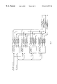
- FIG. 1 the basic structure provided by the AMPIC DRAM device of said copending application is illustrated in FIG. 1, providing a very high bandwidth connection between system I/O resources # 1 #n via corresponding data ports through the DRAM memory array located within the AMPIC DRAM device.
- the flexibility of such an AMPIC DRAM device is further enhanced, as also earlier noted, by the ability to ‘stack’ multiple AMPIC DRAM devices, as illustrated in the example of FIG. 2 .
- FIG. 2 a system consisting of four AMPIC DRAM devices is illustrated, AMPIC # 0 -# 3 , the actual number of AMPIC DRAM devices in a system being limited only by the technology constraints.
- the total DRAM array size available to the system I/O resources is equal to the DRAM array size of each AMPIC DRAM device multiplied by the number of devices in the stack. For example, if each AMPIC DRAM illustrated in FIG. 2 is assumed to contain 64M bits of DRAM, then the AMPIC DRAM stack # 0 -# 3 illustrated will provide a 256M bit DRAM array to the system I/O resources # 1 -# 4 .
- system I/O resource m has a 32K bit message it needs to send to system I/O resource n, then once system I/O resource m has written the message into the AMPIC DRAM array # 0 -# 3 , then a new mechanism must be provided as by the present invention to inform system I/O resource n of both the existence of a message, and of the message location within the AMPIC DRAM array.
- system I/O resource n has been informed of the message existence and of the message location in the AMPIC DRAM array, furthermore, an additional novel mechanism must be provided, again in accordance with the present invention, to allow system I/O resource n to extract the message from the AMPIC DRAM array. It is important to note, as earlier stated, that while the message data is distributed across the entire AMPIC DRAM array, with each element of the array holding only a portion of the data, the complete signaling information must be sent to each individual element of the AMPIC DRAM array.
- system I/O resources may send messages to each other through the AMPIC DRAM array
- system I/O resource m transferring a 32K bit message to system I/O resource n
- the 1 Kbyte internal data bus would allow the message to be transferred between the two system I/O resources in only 2 AMPIC DRAM transfer cycles.
- an AMPIC DRAM transfer cycle is assumed to be 50 nano-seconds (nS) in duration
- the total bandwidth available within the AMPIC DRAM is seen to be 32K bits per 50 nS or 655 gigabits per second.
- This very wide bus is less well suited to transferring small messages between system I/O resources.
- An application where small messages will need to be transferred between system I/O resources, for example, is in ATM networking.
- ATM data is transferred in units of only 424 bits.
- system I/O resources m and n are both ATM network devices, then system I/O resource m may have a 424 bit message to send to system I/O resource n.
- the 32K bit wide internal bus will be used to complete the transfer in only 2 AMPIC DRAM transfer cycles, but a very large amount of the internal bus is wasted in this transfer.
- the present invention discloses an approach whereby the very wide internal data bus will be more efficiently utilized in such situations, further enhancing the usefulness of the AMPIC DRAM architecture by making it equally well suited for small and large units of data transfer.
- CHIP 0 gets data bit 0
- CHIP 1 gets data bit 8
- CHIP 2 gets data bit 16
- CHIP 3 gets data bit 24 .
- all the data bits are incremented. This process continues until the entire message has been sent to the AMPIC DRAM.
- the system I/O resource will also be required to transfer the address at which to place the data in the DRAM.
- the width of the address register in the system I/O resource will be determined by the size of the DRAM array in the AMPIC DRAM and the number of AMPIC DRAM devices in the system.
- a system with four AMPIC DRAM devices each of which contains 64M bits of DRAM, will provide a 256M bit AMPIC DRAM array, requiring 25 address bits.
- Due to the large number of address bits required by large memory arrays it may be necessary to define the address bus between the system I/O resource and the AMPIC DRAM to be narrower than the total address size, and use several transfers to transmit the complete address into the AMPIC DRAM. For example, if the address bus were defined as 4 bits wide, then 7 cycles could be used to transfer the complete 25 bit address into the AMPIC DRAM. This address transfer would take place concurrently with the data transfer from the system I/O resource, as illustrated in FIG. 3 .
- each AMPIC DRAM in the system receives a different portion of the data
- each AMPIC DRAM in the system of FIG. 3 will receive an identical copy of the complete DRAM address, thus causing each AMPIC DRAM to write the message transmitted by the system I/O resource into the same location in the internal DRAM array.
- a Data Valid signal is provided on all the AMPIC DRAM data receive ports.
- the source system I/O resource holds Data Valid asserted for as long as the message data is being transmitted to the AMPIC DRAM, and the AMPIC DRAM uses this assertion of the Data Valid signal to determine the length of the message.
- this bit count is stored along with the message itself.
- the AMPIC DRAM uses this bit count to determine the length of the message to be transmitted.
- the AMPIC DRAM indicates the size of the message to the destination system I/O resource by asserting the Data Valid signal for as long as is indicated by the message bit count.
- each message DRAM address within each AMPIC DRAM device also provides an efficient solution for the case of one system I/O resource having a single message which must be sent to several other system I/O resources, which is illustrated in FIG. 4.
- a message of this type is defined as a multicast message.
- the source system I/O resource writes the message into the AMPIC DRAM in the same way a standard, or unicast, message is written.
- the address of this multicast message within the DRAM array is then forwarded to all of the system I/O resources which are required to receive the message.
- Each of the destination system I/O resources # 1 -#m then proceeds to drive the address of the multicast message into the AMPIC DRAM device.
- the AMPIC DRAM device is provided with the address compare logic, illustrated in FIG. 4, which can compare DRAM addresses received from different system I/O resources
- the multicast control portion of the AMPIC DRAM then recognizes that the same DRAM address was received from each of the multicast message system I/O resources, and only needs to execute a single DRAM read cycle.
- the DRAM data from that read cycle is then forwarded to all of the destination system I/O resources # 1 -#m at the same time by the multicast control logic illustrated in FIG. 4, thus eliminating the requirement of several DRAM reads for multicast messages.
- the total number of address bits required to specify the DRAM location at which to write the message is further reduced by logically partitioning the DRAM into many equally sized sections. For example, in the case of a 256M bit AMPIC DRAM array spread across four AMPIC DRAM devices, the array may be divided, for example, into 2048 bit sections. In this case, the DRAM array would now consist of 128K sections; each AMPIC DRAM device would store 512 bits of each of the 128K sections. As a result, only 17 address bits would be required completely to specify the address to the AMPIC DRAM.
- each DRAM section #A-#C reserves some number of bits to contain what is referred to as a Link Address.
- the system I/O resource m When system I/O resource m has a message to write into the AMPIC DRAM which is larger than the currently defined section size, the system I/O resource will first need to divide the message into several pieces, the size of each being less than or equal to the currently defined section size.
- the first piece of the message will be placed into the first DRAM section, and the Link Address of that section will be set to point to the next DRAM section, into which the second piece of the message will be placed, and so on, until the entire message has been written into the AMPIC DRAM array.
- FIG. 5 The result for an example in which a message occupies 3 DRAM sections is illustrated in FIG. 5 .
- a message size of 5120 bits will be assumed, and the section size will be assumed to be 2048 bits, as explained above.
- bits 1-2048 of the message will reside in DRAM Section #A
- bits 2049-4096 will reside in DRAM Section #B
- bits 4097-5120 will reside in DRAM Section #C, resulting in a partially filled DRAM Section, as illustrated in FIG.
- the AMPIC DRAM reassembles the complete message when sending the message to the destination system I/O resource.
- logic in the AMPIC DRAM examines the section Link Address portion to determine if this DRAM section is one part of a larger message. If the Link Address points to another section of the DRAM, then the AMPIC DRAM reads that section out of the DRAM array for forwarding to the destination port. This process continues until the AMPIC DRAM finds a DRAM section the Link Address of which does not point to another section, at which point the entire message has been reassembled. This message reassembly occurs without any intervention on the part of the destination system I/O resource; it is handled entirely by logic within the AMPIC DRAM.
- the section size is not fixed within the AMPIC, but is instead programmable to a range of different values as illustrated in FIG. 6 .
- the section size may be set to, say, 256 bits.
- the section size may be set to, for example, 2048 bits.
- a range of such sizes would be provided by the AMPIC DRAM device, in order to maximize the use of the DRAM array and minimize wasted memory space caused by messages which are smaller than the section size.
- FIG. 6 an example of three different section sizes, A, B, and C, and the resulting structure of the DRAM array are presented.
- wasted DRAM space may be totally eliminated by not dividing the DRAM array into sections at all, as illustrated in FIG. 7 .
- messages are always placed into the DRAM array back to back, regardless of their size. While increasing the number of address bits required to keep track of DRAM addresses, this embodiment has the advantage of using the memory most efficiently, FIG. 7 illustrating how different-sized messages may be distributed throughout the DRAM array.
- all the passing of addresses between source system I/O resources and destination I/O resources takes place in logic external to the AMPIC DRAM. In an alternate embodiment, this function is handled by the AMPIC DRAM itself, as illustrated in FIG. 8 .
- all addressing and passing of addresses from source system I/O resource to destination system resources takes place inside the AMPIC DRAM itself.
- the system I/O resources need no knowledge of the DRAM address at which messages are located within the AMPIC DRAM array. For example, if the source system I/O resource had a message to send to the destination system resource, then the source system I/O resource would send the message data into the AMPIC DRAMs, without also needing to drive in an address. It should be noted that FIG.
- the AMPIC DRAM Upon receiving the message data, the AMPIC DRAM chooses a free address in its DRAM array from the free address list and writes the message to that location. That address is then forwarded to the AMPIC DRAM port to which the destination system I/O resource is connected. The AMPIC DRAM then informs the destination system I/O resource of the existence of a message for it within the AMPIC DRAM using the Message Ready signal illustrated in FIG. 8 . At some point later, the destination system I/O resource signals that it is ready to accept the message via the Resource Ready signal of FIG.
- each AMPIC DRAM device retrieves its portion of the message data from its DRAM array and forwards the data on to the destination system I/O resource.
- the system I/O resources are made completely independent of the internal structure of the AMPIC DRAM devices; the AMPIC DRAM array functions as a store and forward m X n cross-connect array.
- the AMPIC DRAM in addition to keeping track of the locations of messages in the DRAM array, the AMPIC DRAM must also keep track of the amount of free space remaining in the DRAM array. As the DRAM array begins to fill up, the AMPIC DRAM must be able to signal the system I/O resources not to send any messages for some period of time, until the DRAM array has started to empty out.
- the Free Address List as illustrated in FIG. 8, is used for this purpose.
- the DRAM array of an AMPIC DRAM device is shown physically divided or partitioned into several independently controlled banks; the actual number of DRAM banks implemented (DRAM Banks 1 -m) will depend only on the technology used to implement the AMPIC DRAM.
- DRAM Banks 1 -m the actual number of DRAM banks implemented
- a system consisting of only a single AMPIC DRAM device will accordingly be discussed here, the discussion being equally applicable to systems consisting of multiple AMPIC DRAM devices. In the latter case, the DRAM array in each AMPIC DRAM device will be partitioned identically.
- the number of DRAM banks will be greater than or equal to the number of system I/O resources which can be connected to the AMPIC DRAM.
- the very wide internal data bus is shown in FIG. 9 evenly divided between each of the DRAM banks.
- the data bus for each DRAM bank would be 512 bits wide; the sixty-four 512 bit wide buses would combine to form the complete 32K bit wide data bus.
- each system I/O resource is connected to a data port within the AMPIC DRAM, which in turn connects to the internal very wide data bus.
- FIG. 9 the embodiment illustrated in FIG.
- each of these data ports is divided into a number of slots ( 0 -m); the number of slots in each data port being equal to the number of DRAM banks.
- each data port will be 32K bits wide, and will be divided into 64 sections of 512 bits each.
- Each slot corresponds to a single bank of the DRAM array.
- the entire message may be streamed into all 64 slots of the data port, and then written into the DRAM array in a single AMPIC DRAM write cycle. If an illustrative value of 50 nS is once again assumed for the duration of an AMPIC DRAM transfer cycle, the resultant internal AMPIC DRAM bandwidth is seen to be 32K bits per 50 nS or 655 gigabits per second.
- a single system resource may be allowed to accumulate multiple short messages, filling several slots of its data port before writing the message data into the DRAM array. It should be noted that a single system I/O resource may only accumulate several short messages in its data port if each of the messages is destined for a different DRAM bank, as indicated by the message addresses.
- up to 64 messages may be transferred within the AMPIC DRAM simultaneously, whether from the same system I/O resource, or from many different system I/O resources.
- the utilized bandwidth for ATM networking is therefore calculated to be (64*424) bits per 50 nS or 542 gigabits per second, or almost 83% of the total available bandwidth. This total bandwidth utilization will increase as the number of DRAM banks provided in the AMPIC DRAM device is increased.
- the DRAM and buffering structure herein disclosed therefore, provides a balance between support of small numbers of very wide data transfers, and larger numbers of small data transfers, by allowing several small data transfers from different system I/O resources to occur simultaneously.
- FIG. 10 An alternate embodiment of the invention for alleviating this problem is illustrated in FIG. 10 .
- an mXn crossbar switch is placed between each system resource data port ( 1 -n) and the DRAM array (banks 1 -m).
- the DRAM array consists of m banks and the buffer consists of s slots.
- the crossbar switch enables any section of the buffer to be driven to any one of the DRAM banks, therefore making the buffer independent of the DRAM address used; rather than controlling into which buffer section the data must be written, the DRAM address will control the functioning of the switch.
- system I/O resource 1 has written 424 bits into data port slot 0 destined for DRAM bank 1
- system I/O resource n has also written 424 bits into slot 1 of its data port destined for DRAM bank m
- both messages may be written into the DRAM simultaneously.
- Logic in the AMPIC DRAM will need to control each port switch appropriately to switch the correct data port slot(s) to the correct DRAM bank(s) for each transfer.
- this switch will also need to operate bidirectionally; that is, for reads of the DRAM where data is to be transmitted from the AMPIC DRAM to a system I/O resource, the switch must be able to move data from the correct DRAM banks into the proper data port slots.
- the crossbar switch in this alternate embodiment allows for much more flexible use of the entire data port.
- the second message is now written into the next available slot of the data port, regardless of its eventual destination DRAM bank.
- the mXn crossbar switch is used to forward the message to the appropriate DRAM bank when the time comes to write the message into the DRAM.
Abstract
Description
Claims (38)
Priority Applications (10)
| Application Number | Priority Date | Filing Date | Title |
|---|---|---|---|
| US08/901,502 US6212597B1 (en) | 1997-07-28 | 1997-07-28 | Apparatus for and method of architecturally enhancing the performance of a multi-port internally cached (AMPIC) DRAM array and like |
| CA002297836A CA2297836C (en) | 1997-07-28 | 1998-07-23 | Multi-port internally cached drams |
| AU82367/98A AU748133B2 (en) | 1997-07-28 | 1998-07-23 | Multi-port internally cached drams |
| CNB988077248A CN1159655C (en) | 1997-07-28 | 1998-07-23 | Multi-port internally cached DRAMS |
| PCT/IB1998/001121 WO1999005604A1 (en) | 1997-07-28 | 1998-07-23 | Multi-port internally cached drams |
| EP98932443A EP1015989B1 (en) | 1997-07-28 | 1998-07-23 | Multi-port internally cached drams |
| JP2000504513A JP4046943B2 (en) | 1997-07-28 | 1998-07-23 | Multiport internal cache DRAM |
| DE69810132T DE69810132T2 (en) | 1997-07-28 | 1998-07-23 | MULTIPORT DRAMS WITH INTERNAL CACHE |
| IL13422298A IL134222A (en) | 1997-07-28 | 1998-07-23 | Multi-port internally cached drams |
| HK01101019A HK1030281A1 (en) | 1997-07-28 | 2001-02-13 | Multi-port internally cached drams. |
Applications Claiming Priority (1)
| Application Number | Priority Date | Filing Date | Title |
|---|---|---|---|
| US08/901,502 US6212597B1 (en) | 1997-07-28 | 1997-07-28 | Apparatus for and method of architecturally enhancing the performance of a multi-port internally cached (AMPIC) DRAM array and like |
Publications (1)
| Publication Number | Publication Date |
|---|---|
| US6212597B1 true US6212597B1 (en) | 2001-04-03 |
Family
ID=25414315
Family Applications (1)
| Application Number | Title | Priority Date | Filing Date |
|---|---|---|---|
| US08/901,502 Expired - Lifetime US6212597B1 (en) | 1997-07-28 | 1997-07-28 | Apparatus for and method of architecturally enhancing the performance of a multi-port internally cached (AMPIC) DRAM array and like |
Country Status (10)
| Country | Link |
|---|---|
| US (1) | US6212597B1 (en) |
| EP (1) | EP1015989B1 (en) |
| JP (1) | JP4046943B2 (en) |
| CN (1) | CN1159655C (en) |
| AU (1) | AU748133B2 (en) |
| CA (1) | CA2297836C (en) |
| DE (1) | DE69810132T2 (en) |
| HK (1) | HK1030281A1 (en) |
| IL (1) | IL134222A (en) |
| WO (1) | WO1999005604A1 (en) |
Cited By (23)
| Publication number | Priority date | Publication date | Assignee | Title |
|---|---|---|---|---|
| US20010038636A1 (en) * | 2000-01-26 | 2001-11-08 | Alliance Semiconductor Corporation | Integrated high speed switch router using a multiport architecture |
| US6567329B2 (en) | 2001-08-28 | 2003-05-20 | Intel Corporation | Multiple word-line accessing and accessor |
| US6574130B2 (en) | 2001-07-25 | 2003-06-03 | Nantero, Inc. | Hybrid circuit having nanotube electromechanical memory |
| US6604176B1 (en) * | 2000-12-21 | 2003-08-05 | Emc Corporation | Data storage system having plural fault domains |
| US20030199172A1 (en) * | 2001-07-25 | 2003-10-23 | Thomas Rueckes | Methods of nanotube films and articles |
| US6643165B2 (en) | 2001-07-25 | 2003-11-04 | Nantero, Inc. | Electromechanical memory having cell selection circuitry constructed with nanotube technology |
| US6706402B2 (en) | 2001-07-25 | 2004-03-16 | Nantero, Inc. | Nanotube films and articles |
| US20040164289A1 (en) * | 2001-12-28 | 2004-08-26 | Nantero, Inc. | Electromechanical three-trace junction devices |
| US6784028B2 (en) | 2001-12-28 | 2004-08-31 | Nantero, Inc. | Methods of making electromechanical three-trace junction devices |
| US20040214366A1 (en) * | 2001-07-25 | 2004-10-28 | Nantero, Inc. | Electromechanical memory array using nanotube ribbons and method for making same |
| US20050256980A1 (en) * | 2004-05-14 | 2005-11-17 | Oki Electric Co., Ltd. | Method for controlling input/output units, and an input/output unit |
| US7016349B1 (en) * | 2000-09-29 | 2006-03-21 | Cypress Semiconductor Corp. | Logic for generating multicast/unicast address (es) |
| US20070248758A1 (en) * | 2002-04-23 | 2007-10-25 | Ward Jonathan W | Methods of using pre-formed nanotubes to make carbon nanotube films, layers, fabrics, elements and articles |
| WO2008086488A3 (en) * | 2007-01-10 | 2008-09-04 | Mobile Semiconductor Corp | Adaptive memory system for enhancing the performance of an external computing device |
| US20080299307A1 (en) * | 2001-07-25 | 2008-12-04 | Ward Jonathan W | Methods of making carbon nanotube films, layers, fabrics, ribbons, elements and articles |
| US20090240897A1 (en) * | 2008-03-21 | 2009-09-24 | Elpida Memory, Inc. | Multi-port memory and system using the same |
| US7738496B1 (en) | 2002-12-31 | 2010-06-15 | Cypress Semiconductor Corporation | Device that provides the functionality of dual-ported memory using single-ported memory for multiple clock domains |
| US7934057B1 (en) | 2003-12-24 | 2011-04-26 | Cypress Semiconductor Corporation | Logic for implementing a dual clock domain read access with predictable timing for bi-directional inputs/outputs |
| US8006026B2 (en) | 2008-03-19 | 2011-08-23 | Elpida Memory, Inc. | Multi-port memory and computer system provided with the same |
| US8145809B1 (en) | 2007-03-09 | 2012-03-27 | Cypress Semiconductor Corporation | Busy detection logic for asynchronous communication port |
| US9514069B1 (en) | 2012-05-24 | 2016-12-06 | Schwegman, Lundberg & Woessner, P.A. | Enhanced computer processor and memory management architecture |
| US9773531B2 (en) | 2012-06-08 | 2017-09-26 | Hewlett Packard Enterprise Development Lp | Accessing memory |
| US20220066699A1 (en) * | 2019-01-16 | 2022-03-03 | Centec Networks (Suzhou) Co., Ltd. | Data read/write method and apparatus, and exchange chip and storage medium |
Families Citing this family (4)
| Publication number | Priority date | Publication date | Assignee | Title |
|---|---|---|---|---|
| CN100390755C (en) * | 2003-10-14 | 2008-05-28 | 中国科学院计算技术研究所 | Computer micro system structure comprising explicit high-speed buffer storage |
| JP4565981B2 (en) * | 2004-11-29 | 2010-10-20 | ソニー・エリクソン・モバイルコミュニケーションズ株式会社 | Nonvolatile memory data storage method, computer program, and portable terminal |
| MA41915A (en) * | 2015-04-07 | 2018-02-13 | Benjamin Gittins | PROGRAMMABLE MEMORY TRANSFER REQUEST UNITS |
| CN113597599A (en) | 2019-03-18 | 2021-11-02 | 拉姆伯斯公司 | System application of DRAM component with cache mode |
Citations (3)
| Publication number | Priority date | Publication date | Assignee | Title |
|---|---|---|---|---|
| US5410540A (en) * | 1992-10-08 | 1995-04-25 | Hitachi, Ltd. | Shared-buffer-type ATM switch having copy function and copy method thereof |
| US5802580A (en) * | 1994-09-01 | 1998-09-01 | Mcalpine; Gary L. | High performance digital electronic system architecture and memory circuit thereof |
| US5875470A (en) * | 1995-09-28 | 1999-02-23 | International Business Machines Corporation | Multi-port multiple-simultaneous-access DRAM chip |
Family Cites Families (9)
| Publication number | Priority date | Publication date | Assignee | Title |
|---|---|---|---|---|
| JPS6339763U (en) * | 1986-08-30 | 1988-03-15 | ||
| JPH0834481B2 (en) * | 1989-07-03 | 1996-03-29 | 日本電気株式会社 | Packet switch |
| JPH0554655A (en) * | 1991-08-22 | 1993-03-05 | Nec Corp | Semiconductor memory device |
| JP2947664B2 (en) * | 1992-03-30 | 1999-09-13 | 株式会社東芝 | Image-dedicated semiconductor storage device |
| US5581773A (en) * | 1992-05-12 | 1996-12-03 | Glover; Michael A. | Massively parallel SIMD processor which selectively transfers individual contiguously disposed serial memory elements |
| US5442747A (en) * | 1993-09-27 | 1995-08-15 | Auravision Corporation | Flexible multiport multiformat burst buffer |
| JPH08241186A (en) * | 1995-03-07 | 1996-09-17 | Fujitsu Ltd | Unit and method for buffer memory management |
| WO1997011419A2 (en) * | 1995-09-08 | 1997-03-27 | Shablamm Computer, Inc. | Synchronous multi-port random access memory |
| US5799209A (en) * | 1995-12-29 | 1998-08-25 | Chatter; Mukesh | Multi-port internally cached DRAM system utilizing independent serial interfaces and buffers arbitratively connected under a dynamic configuration |
-
1997
- 1997-07-28 US US08/901,502 patent/US6212597B1/en not_active Expired - Lifetime
-
1998
- 1998-07-23 EP EP98932443A patent/EP1015989B1/en not_active Expired - Lifetime
- 1998-07-23 AU AU82367/98A patent/AU748133B2/en not_active Expired
- 1998-07-23 CA CA002297836A patent/CA2297836C/en not_active Expired - Fee Related
- 1998-07-23 DE DE69810132T patent/DE69810132T2/en not_active Expired - Lifetime
- 1998-07-23 WO PCT/IB1998/001121 patent/WO1999005604A1/en active IP Right Grant
- 1998-07-23 JP JP2000504513A patent/JP4046943B2/en not_active Expired - Lifetime
- 1998-07-23 IL IL13422298A patent/IL134222A/en not_active IP Right Cessation
- 1998-07-23 CN CNB988077248A patent/CN1159655C/en not_active Expired - Lifetime
-
2001
- 2001-02-13 HK HK01101019A patent/HK1030281A1/en not_active IP Right Cessation
Patent Citations (3)
| Publication number | Priority date | Publication date | Assignee | Title |
|---|---|---|---|---|
| US5410540A (en) * | 1992-10-08 | 1995-04-25 | Hitachi, Ltd. | Shared-buffer-type ATM switch having copy function and copy method thereof |
| US5802580A (en) * | 1994-09-01 | 1998-09-01 | Mcalpine; Gary L. | High performance digital electronic system architecture and memory circuit thereof |
| US5875470A (en) * | 1995-09-28 | 1999-02-23 | International Business Machines Corporation | Multi-port multiple-simultaneous-access DRAM chip |
Cited By (43)
| Publication number | Priority date | Publication date | Assignee | Title |
|---|---|---|---|---|
| US7251249B2 (en) * | 2000-01-26 | 2007-07-31 | Tundra Semiconductor Corporation | Integrated high speed switch router using a multiport architecture |
| US20010038636A1 (en) * | 2000-01-26 | 2001-11-08 | Alliance Semiconductor Corporation | Integrated high speed switch router using a multiport architecture |
| US7016349B1 (en) * | 2000-09-29 | 2006-03-21 | Cypress Semiconductor Corp. | Logic for generating multicast/unicast address (es) |
| US6604176B1 (en) * | 2000-12-21 | 2003-08-05 | Emc Corporation | Data storage system having plural fault domains |
| US20030199172A1 (en) * | 2001-07-25 | 2003-10-23 | Thomas Rueckes | Methods of nanotube films and articles |
| US20040214367A1 (en) * | 2001-07-25 | 2004-10-28 | Nantero, Inc. | Electromechanical memory array using nanotube ribbons and method for making same |
| US6643165B2 (en) | 2001-07-25 | 2003-11-04 | Nantero, Inc. | Electromechanical memory having cell selection circuitry constructed with nanotube technology |
| US6706402B2 (en) | 2001-07-25 | 2004-03-16 | Nantero, Inc. | Nanotube films and articles |
| US20040085805A1 (en) * | 2001-07-25 | 2004-05-06 | Nantero, Inc. | Device selection circuitry constructed with nanotube technology |
| US8101976B2 (en) | 2001-07-25 | 2012-01-24 | Nantero Inc. | Device selection circuitry constructed with nanotube ribbon technology |
| US6574130B2 (en) | 2001-07-25 | 2003-06-03 | Nantero, Inc. | Hybrid circuit having nanotube electromechanical memory |
| US7745810B2 (en) | 2001-07-25 | 2010-06-29 | Nantero, Inc. | Nanotube films and articles |
| US20040214366A1 (en) * | 2001-07-25 | 2004-10-28 | Nantero, Inc. | Electromechanical memory array using nanotube ribbons and method for making same |
| US20030165074A1 (en) * | 2001-07-25 | 2003-09-04 | Nantero, Inc. | Hybrid circuit having nanotube electromechanical memory |
| US6835591B2 (en) | 2001-07-25 | 2004-12-28 | Nantero, Inc. | Methods of nanotube films and articles |
| US6836424B2 (en) | 2001-07-25 | 2004-12-28 | Nantero, Inc. | Hybrid circuit having nanotube electromechanical memory |
| US20050063210A1 (en) * | 2001-07-25 | 2005-03-24 | Nantero, Inc. | Hybrid circuit having nanotube electromechanical memory |
| US20050191495A1 (en) * | 2001-07-25 | 2005-09-01 | Nantero, Inc. | Nanotube films and articles |
| US20080299307A1 (en) * | 2001-07-25 | 2008-12-04 | Ward Jonathan W | Methods of making carbon nanotube films, layers, fabrics, ribbons, elements and articles |
| US20070141746A1 (en) * | 2001-07-25 | 2007-06-21 | Nantero, Inc. | Methods of nanotube films and articles |
| US6567329B2 (en) | 2001-08-28 | 2003-05-20 | Intel Corporation | Multiple word-line accessing and accessor |
| US6784028B2 (en) | 2001-12-28 | 2004-08-31 | Nantero, Inc. | Methods of making electromechanical three-trace junction devices |
| US20040164289A1 (en) * | 2001-12-28 | 2004-08-26 | Nantero, Inc. | Electromechanical three-trace junction devices |
| US7915066B2 (en) | 2001-12-28 | 2011-03-29 | Nantero, Inc. | Methods of making electromechanical three-trace junction devices |
| US20040191978A1 (en) * | 2001-12-28 | 2004-09-30 | Nantero, Inc. | Methods of making electromechanical three-trace junction devices |
| US20070248758A1 (en) * | 2002-04-23 | 2007-10-25 | Ward Jonathan W | Methods of using pre-formed nanotubes to make carbon nanotube films, layers, fabrics, elements and articles |
| US7738496B1 (en) | 2002-12-31 | 2010-06-15 | Cypress Semiconductor Corporation | Device that provides the functionality of dual-ported memory using single-ported memory for multiple clock domains |
| US7934057B1 (en) | 2003-12-24 | 2011-04-26 | Cypress Semiconductor Corporation | Logic for implementing a dual clock domain read access with predictable timing for bi-directional inputs/outputs |
| US20050256980A1 (en) * | 2004-05-14 | 2005-11-17 | Oki Electric Co., Ltd. | Method for controlling input/output units, and an input/output unit |
| US8504793B2 (en) | 2007-01-10 | 2013-08-06 | Mobile Semiconductor Corporation | Adaptive memory system for enhancing the performance of an external computing device |
| US20090024819A1 (en) * | 2007-01-10 | 2009-01-22 | Mobile Semiconductor Corporation | Adaptive memory system for enhancing the performance of an external computing device |
| US9424182B2 (en) | 2007-01-10 | 2016-08-23 | Mobile Semiconductor Corporation | Adaptive memory system for enhancing the performance of an external computing device |
| WO2008086488A3 (en) * | 2007-01-10 | 2008-09-04 | Mobile Semiconductor Corp | Adaptive memory system for enhancing the performance of an external computing device |
| US8135933B2 (en) | 2007-01-10 | 2012-03-13 | Mobile Semiconductor Corporation | Adaptive memory system for enhancing the performance of an external computing device |
| US8918618B2 (en) | 2007-01-10 | 2014-12-23 | Mobile Semiconductor Corporation | Adaptive memory system for enhancing the performance of an external computing device |
| US8145809B1 (en) | 2007-03-09 | 2012-03-27 | Cypress Semiconductor Corporation | Busy detection logic for asynchronous communication port |
| US8370543B1 (en) | 2007-03-09 | 2013-02-05 | Cypress Semiconductor Corporation | Busy detection logic for asynchronous communication port |
| US8006026B2 (en) | 2008-03-19 | 2011-08-23 | Elpida Memory, Inc. | Multi-port memory and computer system provided with the same |
| US8209497B2 (en) | 2008-03-21 | 2012-06-26 | Elpida Memory, Inc. | Multi-port memory and system using the same |
| US20090240897A1 (en) * | 2008-03-21 | 2009-09-24 | Elpida Memory, Inc. | Multi-port memory and system using the same |
| US9514069B1 (en) | 2012-05-24 | 2016-12-06 | Schwegman, Lundberg & Woessner, P.A. | Enhanced computer processor and memory management architecture |
| US9773531B2 (en) | 2012-06-08 | 2017-09-26 | Hewlett Packard Enterprise Development Lp | Accessing memory |
| US20220066699A1 (en) * | 2019-01-16 | 2022-03-03 | Centec Networks (Suzhou) Co., Ltd. | Data read/write method and apparatus, and exchange chip and storage medium |
Also Published As
| Publication number | Publication date |
|---|---|
| DE69810132D1 (en) | 2003-01-23 |
| AU748133B2 (en) | 2002-05-30 |
| CA2297836A1 (en) | 1999-02-04 |
| DE69810132T2 (en) | 2003-11-06 |
| CA2297836C (en) | 2006-04-11 |
| JP4046943B2 (en) | 2008-02-13 |
| CN1266517A (en) | 2000-09-13 |
| JP2001511559A (en) | 2001-08-14 |
| EP1015989A1 (en) | 2000-07-05 |
| IL134222A (en) | 2004-07-25 |
| EP1015989B1 (en) | 2002-12-11 |
| HK1030281A1 (en) | 2001-04-27 |
| AU8236798A (en) | 1999-02-16 |
| WO1999005604A1 (en) | 1999-02-04 |
| CN1159655C (en) | 2004-07-28 |
| IL134222A0 (en) | 2001-04-30 |
Similar Documents
| Publication | Publication Date | Title |
|---|---|---|
| US6212597B1 (en) | Apparatus for and method of architecturally enhancing the performance of a multi-port internally cached (AMPIC) DRAM array and like | |
| JP4024875B2 (en) | Method and apparatus for arbitrating access to shared memory for network ports operating at different data rates | |
| EP0714534B1 (en) | Multiple-port shared memory interface and associated method | |
| JP3899085B2 (en) | Network equipment | |
| EP0870303B1 (en) | High performance universal multi-port internally cached dynamic random access memory system, architecture and method | |
| EP0993680B1 (en) | Method and apparatus in a packet routing switch for controlling access at different data rates to a shared memory | |
| EP1045558B1 (en) | Very wide memory TDM switching system | |
| US6205523B1 (en) | Memory access with plural memories written with the same data | |
| WO1997024725A9 (en) | High performance universal multi-port internally cached dynamic random access memory system, architecture and method | |
| US6697362B1 (en) | Distributed switch memory architecture | |
| US6138219A (en) | Method of and operating architectural enhancement for multi-port internally cached dynamic random access memory (AMPIC DRAM) systems, eliminating external control paths and random memory addressing, while providing zero bus contention for DRAM access | |
| US7535898B2 (en) | Distributed switch memory architecture | |
| KR100310568B1 (en) | Input port switching protocol for a random access memory | |
| GB2377138A (en) | Ring Bus Structure For System On Chip Integrated Circuits | |
| US6336145B2 (en) | Interprocessor communication interface with message unit coupled to next interface and to internal receive and send buffer | |
| KR100388342B1 (en) | Multi-ported memory with asynchronous and synchronous protocol | |
| JP3703532B2 (en) | Computer system with multiplexed address bus | |
| US5774653A (en) | High-throughput data buffer |
Legal Events
| Date | Code | Title | Description |
|---|---|---|---|
| AS | Assignment |
Owner name: NEONET, LLC, MASSACHUSETTS Free format text: ASSIGNMENT OF ASSIGNORS INTEREST;ASSIGNORS:CONLIN, RICHARD;WRIGHT, TIM;MARCONI, PETER;AND OTHERS;REEL/FRAME:008769/0791 Effective date: 19970723 |
|
| STCF | Information on status: patent grant |
Free format text: PATENTED CASE |
|
| FPAY | Fee payment |
Year of fee payment: 4 |
|
| FEPP | Fee payment procedure |
Free format text: PAYOR NUMBER ASSIGNED (ORIGINAL EVENT CODE: ASPN); ENTITY STATUS OF PATENT OWNER: LARGE ENTITY Free format text: PAYER NUMBER DE-ASSIGNED (ORIGINAL EVENT CODE: RMPN); ENTITY STATUS OF PATENT OWNER: LARGE ENTITY |
|
| FEPP | Fee payment procedure |
Free format text: PAT HOLDER NO LONGER CLAIMS SMALL ENTITY STATUS, ENTITY STATUS SET TO UNDISCOUNTED (ORIGINAL EVENT CODE: STOL); ENTITY STATUS OF PATENT OWNER: LARGE ENTITY |
|
| REMI | Maintenance fee reminder mailed | ||
| FPAY | Fee payment |
Year of fee payment: 8 |
|
| SULP | Surcharge for late payment |
Year of fee payment: 7 |
|
| FPAY | Fee payment |
Year of fee payment: 12 |
|
| AS | Assignment |
Owner name: CREDIT SUISSE AG, NEW YORK Free format text: SECURITY INTEREST;ASSIGNOR:ALCATEL-LUCENT USA INC.;REEL/FRAME:030510/0627 Effective date: 20130130 |
|
| AS | Assignment |
Owner name: ALCATEL-LUCENT USA INC., NEW JERSEY Free format text: RELEASE BY SECURED PARTY;ASSIGNOR:CREDIT SUISSE AG;REEL/FRAME:033950/0261 Effective date: 20140819 |
|
| AS | Assignment |
Owner name: PROVENANCE ASSET GROUP LLC, CONNECTICUT Free format text: ASSIGNMENT OF ASSIGNORS INTEREST;ASSIGNORS:NOKIA TECHNOLOGIES OY;NOKIA SOLUTIONS AND NETWORKS BV;ALCATEL LUCENT SAS;REEL/FRAME:043877/0001 Effective date: 20170912 Owner name: NOKIA USA INC., CALIFORNIA Free format text: SECURITY INTEREST;ASSIGNORS:PROVENANCE ASSET GROUP HOLDINGS, LLC;PROVENANCE ASSET GROUP LLC;REEL/FRAME:043879/0001 Effective date: 20170913 Owner name: CORTLAND CAPITAL MARKET SERVICES, LLC, ILLINOIS Free format text: SECURITY INTEREST;ASSIGNORS:PROVENANCE ASSET GROUP HOLDINGS, LLC;PROVENANCE ASSET GROUP, LLC;REEL/FRAME:043967/0001 Effective date: 20170913 |
|
| AS | Assignment |
Owner name: NOKIA US HOLDINGS INC., NEW JERSEY Free format text: ASSIGNMENT AND ASSUMPTION AGREEMENT;ASSIGNOR:NOKIA USA INC.;REEL/FRAME:048370/0682 Effective date: 20181220 |
|
| AS | Assignment |
Owner name: PROVENANCE ASSET GROUP LLC, CONNECTICUT Free format text: RELEASE BY SECURED PARTY;ASSIGNOR:CORTLAND CAPITAL MARKETS SERVICES LLC;REEL/FRAME:058983/0104 Effective date: 20211101 Owner name: PROVENANCE ASSET GROUP HOLDINGS LLC, CONNECTICUT Free format text: RELEASE BY SECURED PARTY;ASSIGNOR:CORTLAND CAPITAL MARKETS SERVICES LLC;REEL/FRAME:058983/0104 Effective date: 20211101 Owner name: PROVENANCE ASSET GROUP LLC, CONNECTICUT Free format text: RELEASE BY SECURED PARTY;ASSIGNOR:NOKIA US HOLDINGS INC.;REEL/FRAME:058363/0723 Effective date: 20211129 Owner name: PROVENANCE ASSET GROUP HOLDINGS LLC, CONNECTICUT Free format text: RELEASE BY SECURED PARTY;ASSIGNOR:NOKIA US HOLDINGS INC.;REEL/FRAME:058363/0723 Effective date: 20211129 |
|
| AS | Assignment |
Owner name: RPX CORPORATION, CALIFORNIA Free format text: ASSIGNMENT OF ASSIGNORS INTEREST;ASSIGNOR:PROVENANCE ASSET GROUP LLC;REEL/FRAME:059352/0001 Effective date: 20211129 |