US6215920B1 - Electrophoretic, high index and phase transition control of total internal reflection in high efficiency variable reflectivity image displays - Google Patents
Electrophoretic, high index and phase transition control of total internal reflection in high efficiency variable reflectivity image displays Download PDFInfo
- Publication number
- US6215920B1 US6215920B1 US09/324,103 US32410399A US6215920B1 US 6215920 B1 US6215920 B1 US 6215920B1 US 32410399 A US32410399 A US 32410399A US 6215920 B1 US6215920 B1 US 6215920B1
- Authority
- US
- United States
- Prior art keywords
- image display
- prismatic
- sheet
- display device
- liquid
- Prior art date
- Legal status (The legal status is an assumption and is not a legal conclusion. Google has not performed a legal analysis and makes no representation as to the accuracy of the status listed.)
- Expired - Lifetime
Links
Images


Classifications
-
- G—PHYSICS
- G02—OPTICS
- G02F—OPTICAL DEVICES OR ARRANGEMENTS FOR THE CONTROL OF LIGHT BY MODIFICATION OF THE OPTICAL PROPERTIES OF THE MEDIA OF THE ELEMENTS INVOLVED THEREIN; NON-LINEAR OPTICS; FREQUENCY-CHANGING OF LIGHT; OPTICAL LOGIC ELEMENTS; OPTICAL ANALOGUE/DIGITAL CONVERTERS
- G02F1/00—Devices or arrangements for the control of the intensity, colour, phase, polarisation or direction of light arriving from an independent light source, e.g. switching, gating or modulating; Non-linear optics
- G02F1/01—Devices or arrangements for the control of the intensity, colour, phase, polarisation or direction of light arriving from an independent light source, e.g. switching, gating or modulating; Non-linear optics for the control of the intensity, phase, polarisation or colour
- G02F1/165—Devices or arrangements for the control of the intensity, colour, phase, polarisation or direction of light arriving from an independent light source, e.g. switching, gating or modulating; Non-linear optics for the control of the intensity, phase, polarisation or colour based on translational movement of particles in a fluid under the influence of an applied field
- G02F1/166—Devices or arrangements for the control of the intensity, colour, phase, polarisation or direction of light arriving from an independent light source, e.g. switching, gating or modulating; Non-linear optics for the control of the intensity, phase, polarisation or colour based on translational movement of particles in a fluid under the influence of an applied field characterised by the electro-optical or magneto-optical effect
- G02F1/167—Devices or arrangements for the control of the intensity, colour, phase, polarisation or direction of light arriving from an independent light source, e.g. switching, gating or modulating; Non-linear optics for the control of the intensity, phase, polarisation or colour based on translational movement of particles in a fluid under the influence of an applied field characterised by the electro-optical or magneto-optical effect by electrophoresis
-
- G—PHYSICS
- G02—OPTICS
- G02B—OPTICAL ELEMENTS, SYSTEMS OR APPARATUS
- G02B26/00—Optical devices or arrangements for the control of light using movable or deformable optical elements
- G02B26/02—Optical devices or arrangements for the control of light using movable or deformable optical elements for controlling the intensity of light
-
- G—PHYSICS
- G02—OPTICS
- G02B—OPTICAL ELEMENTS, SYSTEMS OR APPARATUS
- G02B5/00—Optical elements other than lenses
- G02B5/04—Prisms
- G02B5/045—Prism arrays
-
- G—PHYSICS
- G02—OPTICS
- G02F—OPTICAL DEVICES OR ARRANGEMENTS FOR THE CONTROL OF LIGHT BY MODIFICATION OF THE OPTICAL PROPERTIES OF THE MEDIA OF THE ELEMENTS INVOLVED THEREIN; NON-LINEAR OPTICS; FREQUENCY-CHANGING OF LIGHT; OPTICAL LOGIC ELEMENTS; OPTICAL ANALOGUE/DIGITAL CONVERTERS
- G02F1/00—Devices or arrangements for the control of the intensity, colour, phase, polarisation or direction of light arriving from an independent light source, e.g. switching, gating or modulating; Non-linear optics
- G02F1/01—Devices or arrangements for the control of the intensity, colour, phase, polarisation or direction of light arriving from an independent light source, e.g. switching, gating or modulating; Non-linear optics for the control of the intensity, phase, polarisation or colour
- G02F1/165—Devices or arrangements for the control of the intensity, colour, phase, polarisation or direction of light arriving from an independent light source, e.g. switching, gating or modulating; Non-linear optics for the control of the intensity, phase, polarisation or colour based on translational movement of particles in a fluid under the influence of an applied field
- G02F1/1675—Constructional details
- G02F1/1677—Structural association of cells with optical devices, e.g. reflectors or illuminating devices
-
- G—PHYSICS
- G02—OPTICS
- G02F—OPTICAL DEVICES OR ARRANGEMENTS FOR THE CONTROL OF LIGHT BY MODIFICATION OF THE OPTICAL PROPERTIES OF THE MEDIA OF THE ELEMENTS INVOLVED THEREIN; NON-LINEAR OPTICS; FREQUENCY-CHANGING OF LIGHT; OPTICAL LOGIC ELEMENTS; OPTICAL ANALOGUE/DIGITAL CONVERTERS
- G02F1/00—Devices or arrangements for the control of the intensity, colour, phase, polarisation or direction of light arriving from an independent light source, e.g. switching, gating or modulating; Non-linear optics
- G02F1/01—Devices or arrangements for the control of the intensity, colour, phase, polarisation or direction of light arriving from an independent light source, e.g. switching, gating or modulating; Non-linear optics for the control of the intensity, phase, polarisation or colour
- G02F1/19—Devices or arrangements for the control of the intensity, colour, phase, polarisation or direction of light arriving from an independent light source, e.g. switching, gating or modulating; Non-linear optics for the control of the intensity, phase, polarisation or colour based on variable-reflection or variable-refraction elements not provided for in groups G02F1/015 - G02F1/169
- G02F1/195—Devices or arrangements for the control of the intensity, colour, phase, polarisation or direction of light arriving from an independent light source, e.g. switching, gating or modulating; Non-linear optics for the control of the intensity, phase, polarisation or colour based on variable-reflection or variable-refraction elements not provided for in groups G02F1/015 - G02F1/169 by using frustrated reflection
-
- G—PHYSICS
- G02—OPTICS
- G02F—OPTICAL DEVICES OR ARRANGEMENTS FOR THE CONTROL OF LIGHT BY MODIFICATION OF THE OPTICAL PROPERTIES OF THE MEDIA OF THE ELEMENTS INVOLVED THEREIN; NON-LINEAR OPTICS; FREQUENCY-CHANGING OF LIGHT; OPTICAL LOGIC ELEMENTS; OPTICAL ANALOGUE/DIGITAL CONVERTERS
- G02F1/00—Devices or arrangements for the control of the intensity, colour, phase, polarisation or direction of light arriving from an independent light source, e.g. switching, gating or modulating; Non-linear optics
- G02F1/29—Devices or arrangements for the control of the intensity, colour, phase, polarisation or direction of light arriving from an independent light source, e.g. switching, gating or modulating; Non-linear optics for the control of the position or the direction of light beams, i.e. deflection
- G02F1/31—Digital deflection, i.e. optical switching
- G02F1/315—Digital deflection, i.e. optical switching based on the use of controlled internal reflection
-
- G—PHYSICS
- G02—OPTICS
- G02F—OPTICAL DEVICES OR ARRANGEMENTS FOR THE CONTROL OF LIGHT BY MODIFICATION OF THE OPTICAL PROPERTIES OF THE MEDIA OF THE ELEMENTS INVOLVED THEREIN; NON-LINEAR OPTICS; FREQUENCY-CHANGING OF LIGHT; OPTICAL LOGIC ELEMENTS; OPTICAL ANALOGUE/DIGITAL CONVERTERS
- G02F1/00—Devices or arrangements for the control of the intensity, colour, phase, polarisation or direction of light arriving from an independent light source, e.g. switching, gating or modulating; Non-linear optics
- G02F1/01—Devices or arrangements for the control of the intensity, colour, phase, polarisation or direction of light arriving from an independent light source, e.g. switching, gating or modulating; Non-linear optics for the control of the intensity, phase, polarisation or colour
- G02F1/165—Devices or arrangements for the control of the intensity, colour, phase, polarisation or direction of light arriving from an independent light source, e.g. switching, gating or modulating; Non-linear optics for the control of the intensity, phase, polarisation or colour based on translational movement of particles in a fluid under the influence of an applied field
- G02F1/1675—Constructional details
- G02F2001/1678—Constructional details characterised by the composition or particle type
-
- G—PHYSICS
- G02—OPTICS
- G02F—OPTICAL DEVICES OR ARRANGEMENTS FOR THE CONTROL OF LIGHT BY MODIFICATION OF THE OPTICAL PROPERTIES OF THE MEDIA OF THE ELEMENTS INVOLVED THEREIN; NON-LINEAR OPTICS; FREQUENCY-CHANGING OF LIGHT; OPTICAL LOGIC ELEMENTS; OPTICAL ANALOGUE/DIGITAL CONVERTERS
- G02F2203/00—Function characteristic
- G02F2203/02—Function characteristic reflective
- G02F2203/026—Function characteristic reflective attenuated or frustrated internal reflection
-
- Y—GENERAL TAGGING OF NEW TECHNOLOGICAL DEVELOPMENTS; GENERAL TAGGING OF CROSS-SECTIONAL TECHNOLOGIES SPANNING OVER SEVERAL SECTIONS OF THE IPC; TECHNICAL SUBJECTS COVERED BY FORMER USPC CROSS-REFERENCE ART COLLECTIONS [XRACs] AND DIGESTS
- Y10—TECHNICAL SUBJECTS COVERED BY FORMER USPC
- Y10S—TECHNICAL SUBJECTS COVERED BY FORMER USPC CROSS-REFERENCE ART COLLECTIONS [XRACs] AND DIGESTS
- Y10S385/00—Optical waveguides
- Y10S385/901—Illuminating or display apparatus
Definitions
- the '161 application discloses a multiple pixel image display device.
- Each pixel has at least one element having a reflective state in which incident light undergoes total internal reflection (“TIR”), and having a non-reflective state in which TIR is prevented (i.e. “frustrated”).
- TIR total internal reflection
- a member is positioned adjacent the element and deformed between first and second positions. In the first position, a gap remains between the member and the element to allow the evanescent wave to have the usual characteristics for TIR. In the second position, the member is in optical contact with the element (that is, the gap thickness is substantially less than an optical wavelength), substantially interfering with the evanescent wave, thus preventing TIR.
- the '214 application discloses a number of improvements to the invention disclosed in the '161 application, including the use of electrophoresis to control the TIR phenomenon, redirection of light through two prismatic surfaces in a manner which permits the TIR phenomenon to occur and to be controlled at a flat surface, and the use of both electrophoresis and dual prismatic surfaces to achieve gapless control of the TIR phenomenon at a flat surface.
- the present invention further improves upon the image displays disclosed in the '161 and '214 applications.
- charged particles suspended in a medium such as FluorinertTM Electronic Liquid are used to electrophoretically control the TIR phenomenon at a retro-reflective surface on a high refractive index material.
- a second embodiment uses a prismatic structure to redirect ambient light from an overhead light source toward a display image and then from the image to the viewing region in front of the image, yielding a high contrast reflective display.
- a third embodiment uses a transparent planar waveguide to frontlight a colour display.
- a fourth embodiment controls the TIR phenomenon at a retro-reflective surface by means of a vapour-liquid phase transition.
- a fifth embodiment controls the TIR phenomenon by changing the absorption coefficient of a material using electrical, chemical and/or electrochemical methods.
- FIG. 1 schematically depicts a light ray undergoing refraction at a glass:air interface.
- FIG. 2 a pictorial illustration, on a greatly enlarged scale, of the operation of a prior art retro-reflector.
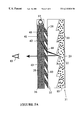
- FIG. 3 is fragmented, cross-sectional view, on a greatly enlarged scale, of a retro-reflective high refractive index prismatic surface in contact with an electrophoretic medium through which particles are selectively transported to modify the optical characteristics of the medium at the prismatic interface at which TIR normally occurs.
- the left side of FIG. 3 shows no electrophoretic activity, such that light rays incident upon the prismatic interface undergo TIR.
- the right side of FIG. 3 shows the particles electrophoretically transported to the prismatic interface, frustrating TIR such that light incident upon the prismatic interface does not undergo TIR.
- FIG. 4A is an isometric view, on a greatly enlarged scale, of a portion of a prismatic, micro-structured surface which can be positioned such that light rays incident upon the surface at a pre-selected angle, in this case 45° ambient light, are directed toward an image, such that the image then reflects the light rays away from the image in a preferred direction for viewing the image.
- a pre-selected angle in this case 45° ambient light
- FIG. 4B is a side elevation view, on a greatly enlarged scale, of a portion of a high reflectivity, high contrast image display incorporating the FIG. 4A micro-structured surface and the FIG. 3 electrophoretic:high index retro-reflective structure.
- FIG. 5A is a cross-sectional view, on a greatly enlarged scale, of a portion of a high reflectivity, high contrast image display incorporating a transparent planar waveguide front light.
- FIG. 5B shows how an array of micro-structured lenses can be incorporated in the FIG. 5A structure to improve extraction of light from the waveguide in a preferential direction.
- FIG. 6 is fragmented, cross-sectional view, on a greatly enlarged scale, of a high reflectivity, high contrast image display in which liquid:vapour phase transitions control TIR.
- the left portion of FIG. 6 shows a vapour created adjacent a prismatic surface to provide a refractive index mis-match whereby incident light rays undergo TIR.
- the centre portion of FIG. 6 shows liquid adjacent the prismatic surface, providing substantial matching of refractive indices whereby TIR is frustrated.
- the right portion of FIG. 6 depicts apertures through which the liquid flows between upper and lower chambers.
- FIG. 7 depicts, on a greatly enlarged scale, a retro-reflective high refractive index prismatic surface to which electrodes are applied to form a metal oxide semiconductor field effect transistor (“MOSFET”) having adjustable reflectivity.
- MOSFET metal oxide semiconductor field effect transistor
- n 1 is the index of refraction of the first medium
- n 2 is the index of refraction of the second medium
- ⁇ 1 is the angle of incidence (or refraction), within the first medium between the light ray and a normal vector to the interface between the two media
- ⁇ 2 is the angle of incidence (or refraction), within the second medium between the light ray and the normal.
- Sin ⁇ 1 increases as the incident portion of ray 10 within the glass diverges away from normal 12 .
- the n 1 /n 2 portion of the argument of the arcsine function exceeds 1 (i.e. for glass, n 1 ⁇ 1.5; and, for air n 2 ⁇ 1; so n 1 /n 2 ⁇ 1.5).
- the maximum value of the sine function is 1, so the arcsine function does not yield real values for values of n 1 /n 2 >1. Consequently, if n 1 /n 2 sin ⁇ 1 ⁇ 1 there is no solution for the refracted angle ⁇ 2 .
- TIR occurs if n 1 /n 2 sin ⁇ 1 ⁇ 1 and the incident light ray is reflected back into the glass.
- Equation (3) shows that the size of the critical angle is related to the ratio of the two indices of refraction. If the difference between the two indices of refraction is relatively large, then the critical angle will be relatively small (i.e. closer to the normal) and vice versa. For purposes of the present invention, smaller critical angles are preferred since they provide a larger range of angles within which TIR may occur. This means that more incident light can be reflected, and it is consequently possible to provide a display device having an improved range of viewing angles, and/or whiter appearance, both of which are desirable characteristics.
- FIG. 2 depicts a corner reflector (also known as a “corner cube”) and shows that an incident light ray undergoes TIR in each of three separate reflections at the three perpendicularly opposed facets which form the corner, with the net result that the light is retro-reflected from the corner reflector in a direction opposite to the direction of the incident ray.
- the air (n ⁇ 1) outside the prismatic facet (n ⁇ 1.6) is replaced with a soft rubber gel (n ⁇ 1.4) the critical angle changes from about 38° to about 61°, preventing reflection of most of the incident light.
- TIR can be frustrated by bringing an elastomeric sheet into “optical contact” with a grouping of retro-reflective elements.
- Optical contact between the elastomeric sheet and the element grouping brings the elastomeric sheet substantially closer than one micron to the grouping, thereby scattering and/or absorbing the evanescent wave adjacent the grouping, thus preventing or frustrating the capability of the corner reflector grouping to totally internally reflect incident light rays.
- FIG. 3 embodiment of the invention facilitates frustration of TIR without the need for mechanical movement of a part such as the aforementioned elastomeric sheet, without the need for maintenance of a gap (i.e. a region of non-optical contact between materials having different refractive indices) whenever TIR is not to be frustrated, and without the need for a flat surface at the TIR interface.
- a gap i.e. a region of non-optical contact between materials having different refractive indices
- FIG. 3 depicts an image display device in which a sheet 19 of high refractive index material is positioned with flat viewing surface 28 outward and retro-reflective prism-bearing surface 29 inward.
- Prisms 27 on surface 29 may have any one of a wide range of prism or near-prism shapes, the only requirement being that prisms 27 be capable of retro-reflecting incident light rays unless TIR is frustrated as hereinafter explained.
- prisms 27 may be conventional “corner cube” reflectors. In the example shown, prisms 27 are inclined at an angle of 45° relative to a vector normal to flat surface 28 .
- Sheet 19 may, for example, be a thin layer of zinc sulfide (ZnS, n ⁇ 2.4), titanium dioxide (TiO 2 , n ⁇ 2.5), niobium pentoxide (NbO 5 , n ⁇ 2.3) or zirconium oxide (ZrO, n ⁇ 2.1).
- Prisms 27 may be formed on surface 29 by machining an initially flat sheet to generate prisms 27 ; or, by depositing high refractive index material via sputtering or evaporation techniques into a machined mould constituting a physical “negative” of the desired retro-reflective prism-bearing surface 29 .
- Prisms 27 need only be about 2 microns deep, and sheet 19 need only be sufficiently thick (i.e.
- any such additional sheet should be designed to minimize refraction of incident light rays and thus minimize the impact of such additional sheet on the optical characteristics of the device as hereinafter explained.
- An electrophoresis medium 20 is maintained in contact with prismatic surface 29 by containment of medium 20 within a reservoir 85 defined by lower sheet 30 .
- a low refractive index, low viscosity, electrically insulating liquid such as FluorinertTM Electronic Liquid FC-72 (n ⁇ 1.25) or FC-75 (n ⁇ 1.27) heat transfer media available from 3M, St. Paul, Minn. functions remarkably well as an electrophoresis medium in practising the present invention.
- a Fuorinert:ZnS TIR interface is thus formed (assuming ZnS is used to form sheet 19 ).
- Medium 20 contains a finely dispersed suspension of light scattering and/or absorptive particles 21 such as dyed or otherwise scattering/absorptive silica particles (n ⁇ 1.44), dyed or otherwise scattering/absorptive latex particles (n ⁇ 1.5), etc.
- the optical characteristics of sheet 30 are relatively unimportant; sheet 30 need only form a reservoir for containment of electrophoresis medium 20 and particles 21 .
- the reflected light ray then encounters a second prism face, opposite the first prism face, and again undergoes TIR at the second prism face, because the 45° angle at which the reflected ray encounters the second prism face (which also forms part of the ZnS:Fluorinert TIR interface) exceeds the interface's 32° critical angle.
- the retro-reflected ray is re-emitted through the ZnS:air interface and emerges, as illustrated, in a direction nearly 180° opposite to the direction of the original incident ray, thus achieving a “white” appearance in the reflected light.
- prisms 29 are corner reflectors, or other three dimensional retro-reflective structures, then incident ray 25 undergoes TIR three times at retro-reflective surface 29 before being re-emitted through the ZnS:air interface in a direction nearly 180° opposite to the direction of the original incident ray.
- a voltage can be applied across medium 20 via electrodes 23 , 22 which are respectively deposited on surfaces 29 , 30 .
- Electrode 23 is transparent and substantially thin such that it does not interfere with incident rays at the ZnS:Fluorinert TIR interface.
- Electrode 22 need not be transparent. If electrophoresis medium 20 is activated by actuating voltage source 24 to apply a voltage across medium 20 , as is illustrated for the right half of medium 20 depicted in FIG. 3, suspended particles 21 are electrophoretically moved to within about 0.25 micron of the ZnS:Fluorinert interface (i.e. inside the evanescent wave region).
- “Electrophoresis” is a well-known phenomenon whereby a charged species (i.e.
- particles 21 scatter or absorb light, by causing a refractive index mismatch at the ZnS:Fluorinert interface. This is illustrated by light ray 26 in FIG. 3, which is scattered and/or absorbed as it strikes particles 21 inside the evanescent wave region at the ZnS:Fluorinert interface, thus achieving a “dark” appearance in the non-reflective absorption region.
- the optical characteristics of surface 29 can be controlled by controlling the voltage applied across medium 20 via electrodes 22 , 23 . Moreover, the electrodes can be segmented to control the electrophoretic activation of medium 20 across separate regions or “pixels” of surface 29 , thus forming an image display.
- a key characteristic of the FIG. 3 embodiment of the invention is the large refractive index mismatch between sheet 19 and electrophoretic medium 20 . If the index mismatch is insufficient to attain the critical angle at the TIR interface, then the structure depicted in FIG. 3 will not work. In such case, a pair of prismatic surfaces can be used to ensure that the incident light rays encounter the TIR interface at the requisite angle, as is described in relation to the FIG. 5A embodiment of the '214 application.
- the FIG. 3 embodiment of the present invention provides an important simplification by dispensing with the need for dual prismatic surfaces.
- Fluorinerts are well also suited to use in displays formed in accordance with the invention because they are good electrical insulators, and they are inert. Fluorinerts also have low viscosity and high density, so particles suspended in Fluorinerts can be moved electrophoretically relatively easily.
- ZnS is a preferred high refractive index material suitable for use in forming sheet 19 .
- the sheet is preferably optically clear and has a high refractive index of approximately 2.4 in the range of visible wavelengths of light.
- optical clarity it is meant that a substantial fraction of light incident on the material at normal incidence will pass through a selected thickness of the material, with only a small fraction of such light being scattered and/or absorbed by the material. Diminished optical clarity is caused by such scattering and/or absorption, typically a combination of both, as the light passes through the material.
- sheet 19 need only be approximately 10 microns thick.
- ZnS is also well suited to use in displays formed in accordance with the invention because it has low absorption/scattering characteristics and consequently high optical clarity in the aforementioned wavelength range. Further, ZnS is available in sheet form and can be machined to yield the desired retro-reflective microstructure as explained above.
- particles 21 When particles 21 move into the evanescent wave region they must be capable of frustrating TIR at the ZnS:Fluorinert interface, by scattering and/or absorbing the evanescent wave.
- particles 21 may be as large as one micron in diameter, the particles' diameter is preferably significantly sub-optical (i.e. an order of magnitude smaller than one micron, say 100 nm in diameter) such that a monolayer of particles at the TIR interface entirely fills the evanescent wave region.
- the diameter of particles 21 is about one micron, but the image display device's contrast ratio is reduced because the ability of particles 21 to pack closely together at the TIR interface is limited by their diameter. More particularly, near the critical angle, the evanescent wave extends quite far into medium 20 , so particles having a diameter of about one micron are able to scatter and/or absorb the wave and thereby frustrate TIR. But, as the angle at which incident light rays strike the TIR interface increases relative to the critical angle, the depth of the evanescent wave region decreases significantly. Relatively large (i.e. one micron) diameter particles cannot be packed as closely into this reduced depth region and accordingly such particles are unable to frustrate TIR to the desired extent. Smaller diameter (i.e. 100 nm) particles can however be closely packed into this reduced depth region and accordingly such particles are able to frustrate TIR for incident light rays which strike the TIR interface at angles exceeding the critical angle.
- FIG. 4B schematically depicts an image display device 31 in which a prismatically structured sheet 35 (FIG. 4A) of high refractive index material is interposed between device 31 and the observer 83 .
- sheet 35 in its vertical operational orientation, sheet 35 has a flat outward face 80 and an opposed inward face bearing a vertically stacked plurality of horizontally extending prismatic segments 32 .
- Each segment 32 consists of a plurality of vertically inclined, parallel prisms 81 .
- ⁇ is the angle of incident ambient light (typically 45°)
- n 2 is the index of refraction of the medium adjacent outward face 80 through which the ambient light passes (i.e. air, n 2 ⁇ 1)
- n 1 is the index of refraction of the structured material comprising sheet 35 . If the material comprising sheet 35 is ZnS (n 1 ⁇ 2.4) then ⁇ ⁇ 8.5°.
- Prisms 81 and segments 32 may be formed by machining an initially flat sheet; or, by depositing a high refractive index material via sputtering or evaporation techniques into a machined mould constituting a physical “negative” of the desired prism-bearing structure.
- Prisms 81 need only be about 2 microns deep, and sheet 35 need only be sufficiently thick (i.e. 5-10 microns) to facilitate provision of a generally but not perfectly flat outward viewing surface 80 . If sheet 35 is insufficiently thick to be self-supporting, an additional sheet (not shown) can be affixed to surface 80 to provide the necessary support. Any such additional sheet should be designed to minimize refraction of incident light rays and thus minimize the impact of such additional sheet on the optical characteristics of the device as hereinafter explained.
- an incident light ray 34 emanating from overhead light source 82 strikes outward, vertically oriented, face 80 at approximately 45°.
- Ray 34 is refracted by sheet 35 .
- the refraction angle is about 28°.
- the refracted ray then encounters one of inclined prisms 81 at about 8.5°, and is specularly reflected therefrom. Since prism segments 32 are also inclined at 8.5°, specular reflection of ray 34 by one of inclined prisms 81 results in TIR of ray 34 toward observer 83 , as illustrated.
- sheet 35 can be positioned to redirect ambient light which strikes sheet 35 at about 45° from above observer 83 , toward the image display surface at which the light undergoes TIR and is redirected toward observer 83 .
- the length dimension of prism segments 32 should be substantially (i.e. 10 to 100 times) larger than the height dimension of each of prisms 81 . This facilitates specular reflection as aforesaid in a manner which minimizes optical interference at the “step” boundaries between the inwardly recessed edge of one segment 32 and the upwardly protruding edge of the immediately adjacent segment. An appropriate design trade off must be made in minimizing the total number of such “step” boundaries, without substantially increasing the thickness of sheet 35 .
- FIG. 3 and 4A embodiments can be combined to yield an image display device 31 (FIG. 4B) in which TIR is controllably frustrated from the rearward side (i.e. the right side, as viewed in FIG. 4B) of prismatic segments 32 .
- reservoir 85 is defined by sheet 30 behind (i.e. to the right of) sheet 35 .
- Reservoir 85 contains an electrophoretic medium in which a plurality of light scattering and/or absorbing particles are suspended as previously described in relation to FIG. 3 . If the particles are not present in selected portions of the evanescent wave region, ambient light emitted by source 82 is specularly reflected by such portions, which accordingly appear highly reflective or white to observer 83 . However, if the particles are electrophoretically moved into the evanescent wave region, specular reflection of ambient light emitted by source 82 is frustrated at such portions, which accordingly appear dark to observer 83 .
- FIG. 5A shows how the embodiments of FIGS. 3, 4 A and/or 4 B can be adapted for use with an integral planar waveguide front light source, enhancing performance in low ambient light conditions.
- a transparent, planar slab waveguide 36 of the type described in U.S. Pat. No. 5,396,350 is mounted in front of the previously described image display device 31 .
- Light source(s) 37 (which may for example comprise a plurality of light emitting diodes) emit light into waveguide 36 through one or more of the waveguide's elongate edges.
- a transparent micro-structured array 38 is mounted between the waveguide's rearward surface 39 and frontward surface 80 of image display device 31 .
- Array 38 can be any type of micro-structure (i.e. prisms, trapezoids, louvers, etc.) capable of uniformly extracting light rays from waveguide 36 and redirecting the extracted rays toward surface 80 at an incident angle of approximately 45°.
- light rays 40 , 41 emitted by light source 37 undergo TIR as they strike either the frontward or rearward surfaces 43 , 39 of waveguide 36 , thus initially confining such rays within waveguide 36 . But, if a ray strikes rearward surface 39 at a point at which one of the micro-structures comprising array 38 contacts surface 39 , then the conditions necessary for TIR are not satisfied (due to the refractive index mismatch between waveguide 36 and array 38 ), allowing such rays to escape from waveguide 36 and pass through array 38 into image display device 31 .
- rays which escape from waveguide 36 into array 38 are reflected rearwardly of array 38 by side wall 44 at a preferential angle of 45° relative to frontward surface 80 of image display device 31 .
- An array 86 of micro-structured lenses can be provided to further assist in directing light extracted from waveguide 36 toward frontward surface 80 at the preferred 45° angle as aforesaid.
- FIGS. 5A, 5 B embodiments yield high contrast black and white or monochrome images, assuming a white light source.
- light source 37 can be de-energized without substantially affecting the high contrast ratio of the image display device.
- light source 37 may comprise a plurality of red, blue and green light emitting diodes which can be sequentially activated to emit red, blue or green light into waveguide 36 during selected time intervals.
- Such coloured light sources may have various configurations provided they are capable of uniformly emitting light into waveguide 36 for redirection as aforesaid. If coloured light is efficiently emitted into waveguide 36 , the colour of the light which escapes through array 38 for redirection or absorption by image display device 31 is governed by the intensity of light source 37 . Since the colour of the reflected image perceived by observer 83 is dependent upon the colour provided by light source 37 and waveguide 36 as aforesaid, the perceived image's colour can be controlled by controlling the colour of light source 37 .
- red image pixels on display device 31 for perception by observer 83 .
- the selected red pixel(s) on image display device 31 are placed in a highly reflective or “on” state by actuating device 31 such that the particles suspended in electrophoretic medium 20 are not clustered within the evanescent wave region at the TIR interface between prisms 81 and medium 20 over those portions of the display comprising the selected red pixel(s).
- the non-selected pixel(s) i.e.
- the remaining, non-red pixel(s)) are placed in an absorptive or “off” state by actuating device 31 such that the particles suspended in electrophoretic medium 20 are clustered within the evanescent wave region at the TIR interface between prisms 81 and medium 20 over those portions of the display comprising the non-selected pixel(s).
- the red light emitting portions of light source 37 are then actuated to emit red light into waveguide 36 , which is directed toward frontward surface 80 at the preferred 45° angle as aforesaid and then through sheet 35 to the TIR interface.
- the selected (and now highly reflective) pixel(s) reflect the red light.
- Observer 83 accordingly perceives the selected pixel(s) as red.
- selected pixels can be selected and caused to reflect blue or green light in sufficiently rapid succession that observer 83 perceives a full colour image comprised or red, blue and green pixels.
- FIG. 6 depicts an image display device in which phase transitions of a low boiling point liquid are used to controllably frustrate TIR.
- a sheet 50 of a material such as 3M Diamond GradeTM reflective polycarbonate sheeting, is positioned with its flat viewing surface 62 outward and its retro-reflective prism-bearing surface 52 inward.
- the prisms on surface 52 may have any one of a wide range of prism or near-prism shapes, the only requirement being that the prisms be capable of retro-reflecting incident light rays unless TIR is frustrated as hereinafter explained.
- Backing sheet 55 vacuum seals the region beneath retro-reflective prism-bearing surface 52 to form a compartment having first and second chambers 53 , 54 .
- Chambers 53 , 54 can be entirely separate chambers; or as shown in FIG. 6, they may be formed by using a thermal barrier 51 to horizontally divide a single, larger chamber into upper and lower chambers.
- Thermal barrier 51 is a black, light absorbing material having a plurality of apertures 87 (see right portion of FIG. 6 ), through which liquid 56 can flow freely between chambers 53 , 54 .
- Apertures 87 are located around the outer perimeter of barrier 51 to minimize interference with the optical characteristics of viewing surface 62 .
- the optical characteristics and surface profile of sheet backing 55 are not critical. Sheet 55 simply provides a physical and thermal barrier for containment of liquid 56 in chamber 54 .
- Liquid 56 may be FluorinertTM Electronic Liquid FC-72 (n ⁇ 1.25), FC-75 (n ⁇ 1.27), pentane (C 5 H 12 , n ⁇ 1.36) or hexane (C 6 H 14 , n ⁇ 1.38).
- the refractive index of liquid 56 is substantially similar to the refractive index of sheet 50 (i.e. for polycarbonate, n ⁇ 1.6) and liquid 56 is preferably easily vapourized (i.e. has a relatively low boiling point at the pressure within chambers 53 , 54 ).
- Prismatic surface 52 and surface 63 of lower sheet 55 are coated with thin transparent electrode films (not shown) comprised of a material such as a metal oxide.
- Voltage sources 58 , 59 are controllably electrically connected to the electrodes to resistively heat one or the other of the electrodes and thereby vapourize liquid 56 in the region adjacent the heated electrode. More particularly, when voltage source 59 is electrically connected to the electrode on surface 52 , heat generated within the electrode causes a liquid-to-vapour phase transition of the liquid 56 contacting the heated portion of surface 52 , thereby forming vapour barrier 57 between surface 52 and liquid 56 , as seen in the left portion of FIG. 6 .
- vapour barrier 57 When voltage source 59 is disconnected from the electrode on surface 52 , and voltage source 58 is electrically connected to heat the electrode on surface 63 , vapour barrier 57 reverts to the liquid phase at surface 52 ; and, simultaneously liquid 56 in contact with the (now heated) electrode on surface 63 undergoes a phase transition to the vapour state, as shown at 64 in the central portion of FIG. 6 .
- Vapour layer 64 has no optical effect, but reversal of the voltage potentials applied to the electrodes on surfaces 52 , 63 as aforesaid accelerates the vapour-to-liquid phase transition at surface 52 .
- the liquid-to-vapour and vapour-to-liquid phase transitions at surfaces 52 , 63 are thus readily controllable by suitably varying the voltage potentials applied to the electrodes on those surfaces.
- FIG. 6 shows vapour barrier 57 created between liquid 56 and prismatic surface 52 by resistive heating of liquid 56 as aforesaid. Because vapourized Fluorinert has a different refractive index than liquid Fluorinert, there is a refractive index mismatch between prismatic surface 52 (for polycarbonate, n ⁇ 1.6) and vapour layer 57 (n ⁇ 1), provided resistive heating power is continuously applied to maintain vapour layer 57 . Substantially less power is required to maintain vapour layer 57 than to create it, so the structure is reasonably bistable in the sense that only a small amount of current is required to flow through the heating electrodes to maintain the “on” state. This also reduces the overall power consumption of the device during operation.
- a light ray 60 incident upon sheet 50 encounters the polycarbonate:vapour interface between surface 52 and vapour barrier 57 at an angle of about 45° by virtue of the prismatic facets on surface 52 . Since 45° exceeds the critical angle (about 38° for a polycarbonate: vapour interface), ray 60 undergoes TIR twice (or three times, if the prismatic facets are corner reflectors) at surface 52 and emerges through viewing surface 62 in a direction substantially 180° opposite to the incident direction. Since the reflected ray emerges in a direction nearly opposite to the direction of the incident ray, viewing surface 62 exhibits a “white” appearance in the above-described “on” state. A diffuser can be overlaid on viewing surface 62 to enhance its white appearance in the “on” state.
- the resistive heating electrode on prismatic surface 52 can be segmented to facilitate “addressing” of separate regions or “pixels” on surface 52 , thus forming an image display.
- the individual pixels can be of a size comparable to the pixel size of a typical computer display monitor for high resolution applications, or can be as large as a few square centimetres for use in low resolution information displays.
- the pixels are bistable, in the sense that once vapour barrier 57 is created, it remains until the resistive heating voltage is removed, allowing the vapour to cool and condense back into the liquid state.
- High resolution pixels can be formed because the pixel size is determined by the size of the patterned electrodes applied to inward prismatic surface 52 .
- liquid 56 should have a low boiling point such that little input energy is required to vapourize the liquid.
- the input energy requirement can be reduced by maintaining liquid 56 in chambers 53 , 54 at a pressure below atmospheric pressure.
- a material's index of refraction determines the manner in which electromagnetic waves propagate through that material. If the material is a homogeneous dielectric, such as those previously discussed (air, glass, etc.), then the material's electrical conductivity is zero. Accordingly, the vector which characterizes the propagation of electromagnetic waves through the material is real (i.e. has no imaginary components). However, if the material's electrical conductivity is non-zero, then the vector which characterizes the propagation of electromagnetic waves through the material is complex (i.e. has both real and imaginary components).
- n I determines the extent to which electromagnetic waves are absorbed by the conductive material. Such absorption occurs when energy is consumed in the production of a conduction current in the material as it interacts with the electromagnetic wave.
- a conductive material's absorption coefficient is related to n I .
- TIR can be controllably frustrated at the retro-reflective surface. If the material's absorption is low, a light ray incident on the retro-reflective surface undergoes TIR at the surface.
- semiconductor techniques can be used to control a material's conductivity, thereby facilitating control of the material's absorption characteristics such that the material becomes highly absorptive in the evanescent wave region at the retro-reflective surface, controllably frustrating TIR.
- FIG. 7 depicts a metal oxide semiconductor field effect transistor (“MOSFET”) having a channel 65 formed of an n-type semi-conductor material bearing a metal oxide layer 66 .
- Source and drain contacts 67 , 68 are provided at opposed ends of channel 65 . Because it contains a large number of majority charge carriers (i.e. electrons), channel 65 is highly electrically conductive. Accordingly, current flows readily between source 67 and drain 68 if an electrical voltage potential is applied therebetween.
- a gate contact 69 is provided on metal oxide layer 66 . If a highly negative voltage potential is applied to gate 69 , majority charge carriers move out of channel 65 , reducing the channel's conductivity. The density of the majority charge carriers remaining in channel 65 depends upon the magnitude of the electric field in the region of gate 69 . Accordingly, the conductivity of channel 65 can be controlled by controlling the voltage applied to gate 69 .
- the n-type semiconductor material used to fabricate channel 65 is a transparent material having an index of refraction n 1 .
- a series of parallel prisms 72 are formed on the face of channel 65 , opposite metal oxide layer 66 .
- a sheet 70 of transparent material bearing a series of parallel prisms 74 identical to prisms 72 is fixed to sheet 70 such that prisms 72 , 74 are interleaved. That is, the apex portion of each one of prisms 72 is fully inserted between the apex portions of an adjacent pair of prisms 74 ; and, the apex portion of each one of prisms 74 is fully inserted between the apex portions of an adjacent pair of prisms 72 .
- Sheet 70 has an index of refraction n 2 where n 2 >n 1 , and has a flat outward viewing surface 75 .
- the prismatic structure on sheet 70 can be fabricated by deposition of the material via sputtering or evaporation techniques into a machined mould bearing a physical “negative” of the desired retro-reflective prism-bearing surface.
- the outward surface of the deposited layer can be adhered to an additional flat sheet for support.
- the structured substrate can then be removed by a number of methods, such as etching away the substrate using a chemical etchant or by pulling the structured film free of the substrate using differential adhesion.
- Channel 65 can then be fabricated by similarly depositing a layer of n-type semiconductor material onto the structured surface of sheet 70 .
- Well known surface treatment techniques are used to ensure adhesion of the interleaved portions of prisms 72 , 74 .
- channel 65 could be deposited first to generate prisms 72 , with the material forming sheet 70 being subsequently deposited on prisms 72 to produce prisms 74 adherent on prisms 72 in the aforementioned interleaved fashion
- the n-type semiconductor material used to fabricate channel 65 is selected such that the light absorbing characteristics of channel 65 vary as a function of the channel's conductivity. If a high voltage potential is applied to gate 69 , channel 65 is in a low conductivity state, as explained above. When channel 65 is in a low conductivity state, it has very low light absorption. Consequently, incident light ray 71 undergoes TIR at the interface between prisms 72 , 74 and viewing surface 75 has a highly reflective appearance, corresponding to the “on” state of the device. If the voltage applied to gate 69 is low, then channel 65 is in a high conductivity state, as explained above. When channel 65 is in a high conductivity state, it has relatively high light absorption.
- the reflectivity of a selected region (i.e. “pixel”) of the semiconductor material can be electrically controlled to form an image display.
- Semiconductor fabrication technology facilitates fabrication of extremely small structures, so this embodiment of the invention is capable of producing very high resolution displays.
- a p-type semiconductor material can be used to fabricate channel 65 .
- the majority charge carriers are positively-charged “holes” rather than negatively-charged electrons as in an n-type semiconductor, and the positions of source 67 and drain 68 are reversed.
- the density of the majority charge carriers remaining in the channel depends on the magnitude of the electric field in the region of gate 69 , so the channel's conductivity and hence the absorption characteristics at the interface of prisms 72 , 74 can be controlled by suitably controlling the voltage applied to gate 69 .
- An electrochemical change in the property of an electrochromic material has been proposed as a technique for fabricating a flat panel display.
- an electric field applied to an electrochromic material is changed, the material changes from transparent to opaque or coloured.
- the effect is reversible when a voltage of opposite polarity is applied.
- 10,000 or more switching cycles can be achieved.
- a significant disadvantage of electrochromic materials in addition to the switching lifetime limitation, is slow switching speed. It can take several seconds for the absorption characteristics of an electrochromic material to change significantly, which is undesirable in general purpose display (i.e. computer monitor) applications.
- the long switching time is due to the large scale change required to alter the colour of the material throughout the entire electrochromic semiconductor material.
Abstract
Description


Claims (60)

Priority Applications (7)
| Application Number | Priority Date | Filing Date | Title |
|---|---|---|---|
| US09/324,103 US6215920B1 (en) | 1997-06-10 | 1999-06-02 | Electrophoretic, high index and phase transition control of total internal reflection in high efficiency variable reflectivity image displays |
| AU49067/00A AU4906700A (en) | 1999-06-02 | 2000-05-26 | Electrophoretic, high index and phase transition control of total internal reflection in high efficiency variable reflectivity image displays |
| EP00930944A EP1188094A2 (en) | 1999-06-02 | 2000-05-26 | Electrophoretic, high index and phase transition control of total internal reflection in high efficiency variable reflectivity image displays |
| CA002371138A CA2371138C (en) | 1999-06-02 | 2000-05-26 | Electrophoretic, high index, or phase transition control of total internal reflection in high efficiency variable reflectivity image displays |
| PCT/CA2000/000631 WO2000075720A2 (en) | 1999-06-02 | 2000-05-26 | Electrophoretic, high index, or phase transition control of total internal reflection in high efficiency variable reflectivity image displays |
| KR10-2001-7015452A KR100496383B1 (en) | 1999-06-02 | 2000-05-26 | Electrophoretic, high index and phase transition control of total internal reflection in high efficiency variable reflectivity image displays |
| JP2001501936A JP2003501695A (en) | 1999-06-02 | 2000-05-26 | Control of total reflection electrophoretic, high refractive index and phase transition in highly efficient variable reflection image displays |
Applications Claiming Priority (3)
| Application Number | Priority Date | Filing Date | Title |
|---|---|---|---|
| US08/872,161 US5959777A (en) | 1997-06-10 | 1997-06-10 | Passive high efficiency variable reflectivity image display device |
| US09/133,214 US6064784A (en) | 1997-06-10 | 1998-08-13 | Electrophoretic, dual refraction frustration of total internal reflection in high efficiency variable reflectivity image displays |
| US09/324,103 US6215920B1 (en) | 1997-06-10 | 1999-06-02 | Electrophoretic, high index and phase transition control of total internal reflection in high efficiency variable reflectivity image displays |
Related Parent Applications (1)
| Application Number | Title | Priority Date | Filing Date |
|---|---|---|---|
| US09/133,214 Continuation-In-Part US6064784A (en) | 1997-06-10 | 1998-08-13 | Electrophoretic, dual refraction frustration of total internal reflection in high efficiency variable reflectivity image displays |
Publications (1)
| Publication Number | Publication Date |
|---|---|
| US6215920B1 true US6215920B1 (en) | 2001-04-10 |
Family
ID=23262094
Family Applications (1)
| Application Number | Title | Priority Date | Filing Date |
|---|---|---|---|
| US09/324,103 Expired - Lifetime US6215920B1 (en) | 1997-06-10 | 1999-06-02 | Electrophoretic, high index and phase transition control of total internal reflection in high efficiency variable reflectivity image displays |
Country Status (7)
| Country | Link |
|---|---|
| US (1) | US6215920B1 (en) |
| EP (1) | EP1188094A2 (en) |
| JP (1) | JP2003501695A (en) |
| KR (1) | KR100496383B1 (en) |
| AU (1) | AU4906700A (en) |
| CA (1) | CA2371138C (en) |
| WO (1) | WO2000075720A2 (en) |
Cited By (118)
| Publication number | Priority date | Publication date | Assignee | Title |
|---|---|---|---|---|
| US6288843B1 (en) * | 1999-01-06 | 2001-09-11 | Compaq Computer Corporation | Apparatus, method and system for 3-D and panoramic imaging |
| WO2002048764A1 (en) * | 2000-12-15 | 2002-06-20 | Scram Technologies, Inc. | A high contrast front projection display panel and a method of making a high contrast front projection display panel |
| US6437921B1 (en) | 2001-08-14 | 2002-08-20 | The University Of British Columbia | Total internal reflection prismatically interleaved reflective film display screen |
| US6452734B1 (en) | 2001-11-30 | 2002-09-17 | The University Of British Columbia | Composite electrophoretically-switchable retro-reflective image display |
| US20020131147A1 (en) * | 1998-08-27 | 2002-09-19 | Paolini Richard J. | Electrophoretic medium and process for the production thereof |
| US6473072B1 (en) | 1998-05-12 | 2002-10-29 | E Ink Corporation | Microencapsulated electrophoretic electrostatically-addressed media for drawing device applications |
| US20030011867A1 (en) * | 2001-07-09 | 2003-01-16 | Loxley Andrew L. | Electro-optic display and adhesive composition for use therein |
| US20030011868A1 (en) * | 1998-03-18 | 2003-01-16 | E Ink Corporation | Electrophoretic displays in portable devices and systems for addressing such displays |
| US20030025855A1 (en) * | 2001-07-09 | 2003-02-06 | E Lnk Corporation | Electro-optic display and lamination adhesive |
| US20030038755A1 (en) * | 2001-08-16 | 2003-02-27 | E Ink Corporation | Light modulation by frustration of total internal reflection |
| US20030090455A1 (en) * | 2001-11-09 | 2003-05-15 | Sharp Laboratories Of America, Inc. A Washington Corporation | Backlit display with improved dynamic range |
| US6574025B2 (en) | 1997-09-04 | 2003-06-03 | The University Of British Columbia | Optical switching by controllable frustration of total internal reflection |
| US20030152315A1 (en) * | 2002-02-05 | 2003-08-14 | Oplux, Inc. | Optical switch with reversible electroplating mirrors |
| US20030165016A1 (en) * | 2002-03-04 | 2003-09-04 | Whitehead Lorne A. | Wide viewing angle reflective display |
| WO2002069030A3 (en) * | 2001-02-27 | 2003-12-11 | Univ British Columbia | High dynamic range display devices |
| US6704133B2 (en) | 1998-03-18 | 2004-03-09 | E-Ink Corporation | Electro-optic display overlays and systems for addressing such displays |
| US20040090646A1 (en) * | 2002-09-19 | 2004-05-13 | Takashi Saitoh | Method, program, and apparatus for preventing a reproduction of an anti-copy document, and a medium storing the program |
| US20040112750A1 (en) * | 2002-09-03 | 2004-06-17 | E Ink Corporation | Electrophoretic medium with gaseous suspending fluid |
| US20040136047A1 (en) * | 2002-07-30 | 2004-07-15 | The University Of British Columbia | Self-stabilized electrophoretically frustrated total internal reflection display |
| WO2004083932A1 (en) * | 2003-03-18 | 2004-09-30 | Koninklijke Philips Electronics N.V. | Foil display with increased brightness using a retro reflector |
| US6822782B2 (en) | 2001-05-15 | 2004-11-23 | E Ink Corporation | Electrophoretic particles and processes for the production thereof |
| US20040252360A1 (en) * | 2001-07-09 | 2004-12-16 | E Ink Corporation | Electro-optic display and lamination adhesive for use therein |
| US20050002088A1 (en) * | 2003-05-07 | 2005-01-06 | Nobutaka Ukigaya | Display apparatus |
| US20050006999A1 (en) * | 2000-10-18 | 2005-01-13 | Sharp Kabushiki Kaisha | Luminous display element |
| US20050035941A1 (en) * | 1995-07-20 | 2005-02-17 | Albert Jonathan D. | Retroreflective electrophoretic displaya and materials for making the same |
| US20050105162A1 (en) * | 2001-03-19 | 2005-05-19 | Paolini Richard J.Jr. | Electrophoretic medium and process for the production thereof |
| US20050134302A1 (en) * | 2003-12-18 | 2005-06-23 | Hao Pan | Dynamic gamma for a liquid crystal display |
| US20050164103A1 (en) * | 2004-01-23 | 2005-07-28 | The Lubrizol Corporation, A Corporation Of The State Of Ohio | Structured fluid compositions for electrophoretically frustrated total internal reflection displays |
| US20050162737A1 (en) * | 2002-03-13 | 2005-07-28 | Whitehead Lorne A. | High dynamic range display devices |
| US20050190137A1 (en) * | 2004-02-27 | 2005-09-01 | E Ink Corporation | Backplanes for electro-optic displays |
| US20050213191A1 (en) * | 2004-03-23 | 2005-09-29 | E Ink Corporation | Light modulators |
| US20050248554A1 (en) * | 2004-05-04 | 2005-11-10 | Sharp Laboratories Of America, Inc. | Liquid crystal display with filtered black point |
| US20050248593A1 (en) * | 2004-05-04 | 2005-11-10 | Sharp Laboratories Of America, Inc. | Liquid crystal display with modulated black point |
| US20050248553A1 (en) * | 2004-05-04 | 2005-11-10 | Sharp Laboratories Of America, Inc. | Adaptive flicker and motion blur control |
| US20050248591A1 (en) * | 2004-05-04 | 2005-11-10 | Sharp Laboratories Of America, Inc. | Liquid crystal display with adaptive width |
| US20050248555A1 (en) * | 2004-05-04 | 2005-11-10 | Sharp Laboratories Of America, Inc. | Liquid crystal display with illumination control |
| US20050248592A1 (en) * | 2004-05-04 | 2005-11-10 | Sharp Laboratories Of America, Inc. | Liquid crystal display with reduced black level insertion |
| US20050248524A1 (en) * | 2004-05-04 | 2005-11-10 | Sharp Laboratories Of America, Inc. | Liquid crystal display with colored backlight |
| US20050248520A1 (en) * | 2004-05-04 | 2005-11-10 | Sharp Laboratories Of America, Inc. | Liquid crystal display with temporal black point |
| US20060051492A1 (en) * | 2004-09-03 | 2006-03-09 | Solae, Llc. | High protein snack product |
| US20060104508A1 (en) * | 2004-11-16 | 2006-05-18 | Sharp Laboratories Of America, Inc. | High dynamic range images from low dynamic range images |
| US20060103621A1 (en) * | 2004-11-16 | 2006-05-18 | Sharp Laboratories Of America, Inc. | Technique that preserves specular highlights |
| US20060132511A1 (en) * | 2004-06-14 | 2006-06-22 | Feng Xiao-Fan | System for reducing crosstalk |
| US20060181503A1 (en) * | 2005-02-17 | 2006-08-17 | Sharp Laboratories Of America, Inc. | Black point insertion |
| US20060209418A1 (en) * | 2005-03-16 | 2006-09-21 | The University Of British Columbia | Optically coupled toroidal lens:hemi-bead brightness enhancer for total internal reflection modulated image displays |
| WO2006105165A2 (en) * | 2005-03-31 | 2006-10-05 | Mark Miles Consulting Inc. | Dynamic motile medium |
| US20060256919A1 (en) * | 2003-03-21 | 2006-11-16 | Sectra Mamea Ab | Refractive x-ray element |
| US20070035808A1 (en) * | 2001-07-09 | 2007-02-15 | E Ink Corporation | Electro-optic display and materials for use therein |
| US20070172118A1 (en) * | 2006-01-24 | 2007-07-26 | Sharp Laboratories Of America, Inc. | Method for reducing enhancement of artifacts and noise in image color enhancement |
| US20070172119A1 (en) * | 2006-01-24 | 2007-07-26 | Sharp Laboratories Of America, Inc. | Color enhancement technique using skin color detection |
| US20070242334A1 (en) * | 2006-01-24 | 2007-10-18 | Uni-Pixel Displays, Inc. | Corner-Cube Retroreflectors for Displays |
| US20070247697A1 (en) * | 2003-11-05 | 2007-10-25 | E Ink Corporation | Electro-optic displays, and materials for use therein |
| US20070296909A1 (en) * | 2006-06-27 | 2007-12-27 | Kabushiki Kaisha Toshiba | Display device |
| US20080030832A1 (en) * | 2006-08-02 | 2008-02-07 | E Ink Corporation | Multi-layer light modulator |
| US20080062323A1 (en) * | 2004-11-03 | 2008-03-13 | Koninklijke Philips Electronics, N.V. | High Intensity Display Screen Based Electronic Window |
| US20080094689A1 (en) * | 2004-11-12 | 2008-04-24 | Koninklijke Philips Electronics, N.V. | Bright Full Color Reflective Display |
| WO2008062336A1 (en) * | 2006-11-21 | 2008-05-29 | Koninklijke Philips Electronics, N.V. | Switchable grating based on electrophoretic particle system |
| US20080129677A1 (en) * | 2006-11-30 | 2008-06-05 | Sharp Laboratories Of America, Inc. | Liquid crystal display with area adaptive backlight |
| US7411719B2 (en) | 1995-07-20 | 2008-08-12 | E Ink Corporation | Electrophoretic medium and process for the production thereof |
| US20080285125A1 (en) * | 2007-05-18 | 2008-11-20 | Fujifilm Manufacturing U.S.A. Inc. | Optical panel for front projection under ambient lighting conditions |
| US20080305255A1 (en) * | 2007-06-07 | 2008-12-11 | Fujifilm Manufacturing U.S.A. Inc. | Optical waveguide coating |
| US20080304799A1 (en) * | 2007-06-07 | 2008-12-11 | Fujifilm Manufacturing U.S.A. Inc. | Thermosetting optical waveguide coating |
| US20090122387A1 (en) * | 2006-01-24 | 2009-05-14 | Uni-Pixel Displays, Inc. | Optical microstructures for light extraction and control |
| US20090262414A1 (en) * | 2006-04-19 | 2009-10-22 | The University Of British Columbia | Ionic electrophoresis in tir-modulated reflective image displays |
| US20100002026A1 (en) * | 2007-02-01 | 2010-01-07 | Dolby Laboratories Licensing Corporation | Calibration of displays having spatially-variable backlight |
| US20100085627A1 (en) * | 2006-01-17 | 2010-04-08 | The University Of British Columbia | Microlens-assisted brightness enhancement in reflective image displays |
| US20100214282A1 (en) * | 2009-02-24 | 2010-08-26 | Dolby Laboratories Licensing Corporation | Apparatus for providing light source modulation in dual modulator displays |
| WO2011031802A2 (en) | 2009-09-11 | 2011-03-17 | Dolby Laboratories Licensing Corporation | Displays incorporating leaky reflectors |
| DE10129443B4 (en) * | 2001-06-19 | 2011-08-11 | Robert Bosch GmbH, 70469 | lighting device |
| US7999787B2 (en) | 1995-07-20 | 2011-08-16 | E Ink Corporation | Methods for driving electrophoretic displays using dielectrophoretic forces |
| US8050512B2 (en) | 2004-11-16 | 2011-11-01 | Sharp Laboratories Of America, Inc. | High dynamic range images from low dynamic range images |
| US20120163021A1 (en) * | 2010-12-23 | 2012-06-28 | Microsoft Corporation | Transparent display backlight assembly |
| CN102608822A (en) * | 2005-01-03 | 2012-07-25 | 英特尔公司 | Display using light guide and refractive index control |
| WO2012115993A1 (en) * | 2011-02-25 | 2012-08-30 | Lumitex, Inc. | Display front lighting device |
| US8466852B2 (en) | 1998-04-10 | 2013-06-18 | E Ink Corporation | Full color reflective display with multichromatic sub-pixels |
| US8482698B2 (en) | 2008-06-25 | 2013-07-09 | Dolby Laboratories Licensing Corporation | High dynamic range display using LED backlighting, stacked optical films, and LCD drive signals based on a low resolution light field simulation |
| US20140002428A1 (en) * | 2012-06-27 | 2014-01-02 | Amazon Technologies, Inc. | Dynamic Display Adjustment |
| US20140022511A1 (en) * | 2011-02-28 | 2014-01-23 | Huei Pei Kuo | Front-projection glasses-free, continuous 3d display |
| US8687271B2 (en) | 2002-03-13 | 2014-04-01 | Dolby Laboratories Licensing Corporation | N-modulation displays and related methods |
| US20140119020A1 (en) * | 2012-10-30 | 2014-05-01 | Elwha Llc | Smart Illuminator For Retroreflective Display Device |
| WO2014160552A1 (en) | 2013-03-26 | 2014-10-02 | Clearink Displays Llc | Displaced porous electrode for frustrating tir |
| US8941683B2 (en) | 2010-11-01 | 2015-01-27 | Microsoft Corporation | Transparent display interaction |
| WO2015175518A1 (en) * | 2014-05-12 | 2015-11-19 | Clearink Displays Llc | Two particle total internal reflection image display |
| US9280029B2 (en) | 2013-05-13 | 2016-03-08 | Clearink Displays, Inc. | Registered reflective element for a brightness enhanced TIR display |
| WO2016057613A1 (en) * | 2014-10-08 | 2016-04-14 | Clearink Displays Llc | Color filter registered reflective display |
| CN105579900A (en) * | 2013-09-30 | 2016-05-11 | 清墨显示股份有限公司 | Method and apparatus for front-lit semi-retro-reflective display |
| WO2016130720A1 (en) * | 2015-02-12 | 2016-08-18 | Clearink Displays, Inc. | Multi-electrode total internal reflection image display |
| CN105940344A (en) * | 2014-01-31 | 2016-09-14 | 清墨显示股份有限公司 | Apparatus and method for reflective image display with dielectric layer |
| CN105954955A (en) * | 2014-12-10 | 2016-09-21 | 元太科技工业股份有限公司 | reflective display device |
| US9466246B1 (en) | 2015-03-16 | 2016-10-11 | Amazon Technologies, Inc. | Display stacks with integrated ambient light sensors |
| US20160314750A1 (en) * | 2004-07-27 | 2016-10-27 | E Ink Corporation | Methods for driving electrophoretic displays using dielectrophoretic forces |
| CN106200198A (en) * | 2016-09-29 | 2016-12-07 | 京东方科技集团股份有限公司 | Electronic paper and preparation method thereof |
| US20170023724A1 (en) * | 2014-12-30 | 2017-01-26 | Boe Technology Group Co., Ltd. | Optical Module And Reflective Display Apparatus |
| US20170045796A1 (en) * | 2015-03-26 | 2017-02-16 | Boe Technology Group Co., Ltd. | Light guide plate, backlight unit, display device and display control system |
| US9576694B2 (en) | 2010-09-17 | 2017-02-21 | Drexel University | Applications for alliform carbon |
| US20170160444A1 (en) * | 2015-12-06 | 2017-06-08 | Clearink Displays, Inc. | Textured high refractive index surface for reflective image displays |
| US9684163B2 (en) | 2010-12-03 | 2017-06-20 | E Ink Corporation | Methods, systems, and products for illuminating displays |
| US9740075B2 (en) | 2013-09-10 | 2017-08-22 | Clearink Displays, Inc. | Method and system for perforated reflective film display device |
| US9752932B2 (en) | 2010-03-10 | 2017-09-05 | Drexel University | Tunable electro-optic filter stack |
| US20180003920A1 (en) * | 2016-07-01 | 2018-01-04 | Tdk Taiwan Corp. | Lens driving mechanism |
| US9891370B2 (en) | 2011-11-17 | 2018-02-13 | At&T Intellectual Property I, L.P. | Methods, systems, and products for image displays |
| US9897890B2 (en) | 2014-10-07 | 2018-02-20 | Clearink Displays, Inc. | Reflective image display with threshold |
| US9939707B2 (en) | 2013-07-08 | 2018-04-10 | Clearink Displays, Inc. | TIR-modulated wide viewing angle display |
| US9961744B1 (en) | 2012-06-26 | 2018-05-01 | Amazon Technologies, Inc. | Ambient light sensing for display |
| EP3385783A1 (en) | 2017-04-04 | 2018-10-10 | Telefónica Germany GmbH & Co. OHG | Method for correcting the physiological accommodation of an observer during the viewing of a visual object |
| US20180299661A1 (en) * | 2016-10-31 | 2018-10-18 | Boe Technology Group Co., Ltd. | Display Panel, Driving Method Thereof and Display Device |
| US10203436B2 (en) | 2013-05-22 | 2019-02-12 | Clearink Displays, Inc. | Method and apparatus for improved color filter saturation |
| US10261221B2 (en) | 2015-12-06 | 2019-04-16 | Clearink Displays, Inc. | Corner reflector reflective image display |
| US10331005B2 (en) | 2002-10-16 | 2019-06-25 | E Ink Corporation | Electrophoretic displays |
| US10386691B2 (en) | 2015-06-24 | 2019-08-20 | CLEARink Display, Inc. | Method and apparatus for a dry particle totally internally reflective image display |
| CN110272204A (en) * | 2019-06-28 | 2019-09-24 | 京东方科技集团股份有限公司 | Composite decking glass, total reflection display device, selwnite English glass and preparation method |
| US10444592B2 (en) | 2017-03-09 | 2019-10-15 | E Ink Corporation | Methods and systems for transforming RGB image data to a reduced color set for electro-optic displays |
| US10705404B2 (en) | 2013-07-08 | 2020-07-07 | Concord (Hk) International Education Limited | TIR-modulated wide viewing angle display |
| US10782466B2 (en) | 2016-03-16 | 2020-09-22 | Coretronic Corporation | Backlight module and display apparatus |
| WO2021037951A1 (en) | 2019-08-29 | 2021-03-04 | Merck Patent Gmbh | Electrophoretic fluid |
| CN113167941A (en) * | 2018-11-06 | 2021-07-23 | 协和(香港)国际教育有限公司 | High brightness retroreflector for static and switchable image display |
| US11650422B2 (en) | 2017-10-23 | 2023-05-16 | Vuzix Corporation | Active correction of aberrations in optical systems |
| WO2023231962A1 (en) * | 2022-06-01 | 2023-12-07 | 华为技术有限公司 | Grating, and method and device for fabricating grating |
Families Citing this family (11)
| Publication number | Priority date | Publication date | Assignee | Title |
|---|---|---|---|---|
| US6067185A (en) | 1997-08-28 | 2000-05-23 | E Ink Corporation | Process for creating an encapsulated electrophoretic display |
| US6592234B2 (en) | 2001-04-06 | 2003-07-15 | 3M Innovative Properties Company | Frontlit display |
| US6738051B2 (en) | 2001-04-06 | 2004-05-18 | 3M Innovative Properties Company | Frontlit illuminated touch panel |
| JP3966213B2 (en) * | 2003-04-08 | 2007-08-29 | トヨタ自動車株式会社 | Covering parts for radar equipment |
| GB2404448A (en) * | 2003-07-31 | 2005-02-02 | Qinetiq Ltd | Electrophoretic display device |
| US7952792B2 (en) * | 2007-04-06 | 2011-05-31 | Koninklijke Philips Electronics N.V. | Reflective display and method for manufacturing such a display |
| US8474177B2 (en) | 2008-02-08 | 2013-07-02 | Vereniging Vu-Windesheim | Reflecting device, solar collector, pitched roof provided with a solar collector of this type, and greenhouse |
| KR101139854B1 (en) * | 2010-04-13 | 2012-05-02 | 광주과학기술원 | Particle counter |
| US8379293B2 (en) * | 2010-10-28 | 2013-02-19 | Raytheon Company | Method and apparatus for modulating light |
| US10209530B2 (en) * | 2015-12-07 | 2019-02-19 | E Ink Corporation | Three-dimensional display |
| CN110494771B (en) * | 2017-02-08 | 2022-01-18 | 巨跃控股有限责任公司 | Light steering and focusing by dielectrophoresis |
Citations (33)
| Publication number | Priority date | Publication date | Assignee | Title |
|---|---|---|---|---|
| US3571511A (en) | 1968-10-25 | 1971-03-16 | Hughes Aircraft Co | Drosograph display system |
| US3612653A (en) | 1970-01-20 | 1971-10-12 | Rca Corp | Digital light deflector having liquid and vapor states |
| US3698793A (en) | 1971-03-11 | 1972-10-17 | Kollsman Instr Corp | Solid state display |
| US3730608A (en) | 1971-09-30 | 1973-05-01 | A Castegnier | Electrolytic light modulation systems |
| US3746785A (en) | 1971-11-26 | 1973-07-17 | Bendix Corp | Deflectable membrane optical modulator |
| US3796480A (en) | 1968-12-26 | 1974-03-12 | Perkin Elmer Corp | Membrane light modulator |
| US3987668A (en) | 1975-11-17 | 1976-10-26 | Popenoe Charles H | Light reflective opti-mechanical displacement microindicator |
| US4148563A (en) | 1976-05-06 | 1979-04-10 | Edward Herbert | Transparent or reflective panel |
| US4165155A (en) | 1978-03-27 | 1979-08-21 | International Business Machines Corporation | Amplitude modulation of light beam |
| US4218302A (en) | 1979-08-02 | 1980-08-19 | U.S. Philips Corporation | Electrophoretic display devices |
| US4249814A (en) | 1979-10-01 | 1981-02-10 | Iowa State University Research Foundation, Inc. | Frustrated total internal reflection camera shutter |
| US4324456A (en) | 1979-08-02 | 1982-04-13 | U.S. Philips Corporation | Electrophoretic projection display systems |
| US4391490A (en) | 1981-04-02 | 1983-07-05 | Xerox Corporation | Interface for proximity coupled electro-optic devices |
| US4536061A (en) | 1981-12-11 | 1985-08-20 | Canon Kabushiki Kaisha | Display element |
| US4867515A (en) | 1988-08-05 | 1989-09-19 | Canadian Patents And Development Ltd. | All-optical modulator with a channel waveguide |
| US5045847A (en) | 1988-01-19 | 1991-09-03 | Sanyo Electric Co., Ltd. | Flat display panel |
| US5099343A (en) | 1989-05-25 | 1992-03-24 | Hughes Aircraft Company | Edge-illuminated liquid crystal display devices |
| US5128782A (en) | 1989-08-22 | 1992-07-07 | Wood Lawson A | Liquid crystal display unit which is back-lit with colored lights |
| US5221987A (en) | 1992-04-10 | 1993-06-22 | Laughlin Richard H | FTIR modulator |
| US5283148A (en) | 1992-09-18 | 1994-02-01 | Minnesota Mining And Manufacturing Company | Liquid toners for use with perfluorinated solvents |
| US5301009A (en) | 1983-04-28 | 1994-04-05 | The United States Of America As Represented By The Secretary Of The Army | Frustrated total internal reflection optical power limiter |
| US5317667A (en) | 1992-11-23 | 1994-05-31 | Ford Motor Company | Electrophoretic switch for a light pipe |
| US5319491A (en) | 1990-08-10 | 1994-06-07 | Continental Typographics, Inc. | Optical display |
| US5396350A (en) | 1993-11-05 | 1995-03-07 | Alliedsignal Inc. | Backlighting apparatus employing an array of microprisms |
| DE4343808A1 (en) | 1993-12-22 | 1995-06-29 | Thomson Brandt Gmbh | Light valve for video,graphics and data display |
| US5455709A (en) | 1993-03-23 | 1995-10-03 | Martin Marietta Corporation | Total internal reflection spatial light modulation apparatus and method of fabrication thereof |
| US5530053A (en) | 1994-05-17 | 1996-06-25 | Minnesota Mining And Manufacturing Company | Liquid toners utilizing highly fluorinated solvents |
| US5555558A (en) | 1994-05-27 | 1996-09-10 | Laughlin; Richard H. | Method for switching optical signals |
| US5555327A (en) | 1995-06-07 | 1996-09-10 | Laughlin; Richard H. | Frustrated total internal reflection device |
| US5561541A (en) | 1984-09-05 | 1996-10-01 | The United States Of America As Represented By The Secretary Of The Army | Frustrated total internal reflection optical power limiter |
| US5608837A (en) | 1995-05-15 | 1997-03-04 | Clio Technologies, Inc. | Transmissive type display and method capable of utilizing ambient light |
| US5959777A (en) * | 1997-06-10 | 1999-09-28 | The University Of British Columbia | Passive high efficiency variable reflectivity image display device |
| US6064784A (en) * | 1997-06-10 | 2000-05-16 | The University Of British Columbia | Electrophoretic, dual refraction frustration of total internal reflection in high efficiency variable reflectivity image displays |
Family Cites Families (2)
| Publication number | Priority date | Publication date | Assignee | Title |
|---|---|---|---|---|
| EP0023741A1 (en) * | 1979-08-02 | 1981-02-11 | Koninklijke Philips Electronics N.V. | Electrophoretic image display device |
| US4701772A (en) * | 1986-11-26 | 1987-10-20 | Xerox Corporation | Thermally activated image bar |
-
1999
- 1999-06-02 US US09/324,103 patent/US6215920B1/en not_active Expired - Lifetime
-
2000
- 2000-05-26 EP EP00930944A patent/EP1188094A2/en not_active Withdrawn
- 2000-05-26 AU AU49067/00A patent/AU4906700A/en not_active Abandoned
- 2000-05-26 JP JP2001501936A patent/JP2003501695A/en active Pending
- 2000-05-26 WO PCT/CA2000/000631 patent/WO2000075720A2/en not_active Application Discontinuation
- 2000-05-26 CA CA002371138A patent/CA2371138C/en not_active Expired - Fee Related
- 2000-05-26 KR KR10-2001-7015452A patent/KR100496383B1/en not_active IP Right Cessation
Patent Citations (36)
| Publication number | Priority date | Publication date | Assignee | Title |
|---|---|---|---|---|
| US3571511A (en) | 1968-10-25 | 1971-03-16 | Hughes Aircraft Co | Drosograph display system |
| US3796480A (en) | 1968-12-26 | 1974-03-12 | Perkin Elmer Corp | Membrane light modulator |
| US3612653A (en) | 1970-01-20 | 1971-10-12 | Rca Corp | Digital light deflector having liquid and vapor states |
| US3698793A (en) | 1971-03-11 | 1972-10-17 | Kollsman Instr Corp | Solid state display |
| US3730608A (en) | 1971-09-30 | 1973-05-01 | A Castegnier | Electrolytic light modulation systems |
| US3746785A (en) | 1971-11-26 | 1973-07-17 | Bendix Corp | Deflectable membrane optical modulator |
| US3987668A (en) | 1975-11-17 | 1976-10-26 | Popenoe Charles H | Light reflective opti-mechanical displacement microindicator |
| US4148563A (en) | 1976-05-06 | 1979-04-10 | Edward Herbert | Transparent or reflective panel |
| US4165155A (en) | 1978-03-27 | 1979-08-21 | International Business Machines Corporation | Amplitude modulation of light beam |
| US4324456A (en) | 1979-08-02 | 1982-04-13 | U.S. Philips Corporation | Electrophoretic projection display systems |
| US4218302A (en) | 1979-08-02 | 1980-08-19 | U.S. Philips Corporation | Electrophoretic display devices |
| US4249814A (en) | 1979-10-01 | 1981-02-10 | Iowa State University Research Foundation, Inc. | Frustrated total internal reflection camera shutter |
| US4391490A (en) | 1981-04-02 | 1983-07-05 | Xerox Corporation | Interface for proximity coupled electro-optic devices |
| US4536061A (en) | 1981-12-11 | 1985-08-20 | Canon Kabushiki Kaisha | Display element |
| US5301009A (en) | 1983-04-28 | 1994-04-05 | The United States Of America As Represented By The Secretary Of The Army | Frustrated total internal reflection optical power limiter |
| US5561541A (en) | 1984-09-05 | 1996-10-01 | The United States Of America As Represented By The Secretary Of The Army | Frustrated total internal reflection optical power limiter |
| US5045847A (en) | 1988-01-19 | 1991-09-03 | Sanyo Electric Co., Ltd. | Flat display panel |
| US4867515A (en) | 1988-08-05 | 1989-09-19 | Canadian Patents And Development Ltd. | All-optical modulator with a channel waveguide |
| US5099343A (en) | 1989-05-25 | 1992-03-24 | Hughes Aircraft Company | Edge-illuminated liquid crystal display devices |
| US5128782A (en) | 1989-08-22 | 1992-07-07 | Wood Lawson A | Liquid crystal display unit which is back-lit with colored lights |
| US5319491A (en) | 1990-08-10 | 1994-06-07 | Continental Typographics, Inc. | Optical display |
| US5221987A (en) | 1992-04-10 | 1993-06-22 | Laughlin Richard H | FTIR modulator |
| US5283148A (en) | 1992-09-18 | 1994-02-01 | Minnesota Mining And Manufacturing Company | Liquid toners for use with perfluorinated solvents |
| US5397669A (en) | 1992-09-18 | 1995-03-14 | Minnesota Mining And Manufacturing Company | Liquid toners for use with perfluorinated solvents |
| US5317667A (en) | 1992-11-23 | 1994-05-31 | Ford Motor Company | Electrophoretic switch for a light pipe |
| US5455709A (en) | 1993-03-23 | 1995-10-03 | Martin Marietta Corporation | Total internal reflection spatial light modulation apparatus and method of fabrication thereof |
| US5396350A (en) | 1993-11-05 | 1995-03-07 | Alliedsignal Inc. | Backlighting apparatus employing an array of microprisms |
| DE4343808A1 (en) | 1993-12-22 | 1995-06-29 | Thomson Brandt Gmbh | Light valve for video,graphics and data display |
| US5530067A (en) | 1994-05-17 | 1996-06-25 | Minnesota Mining And Manufacturing Company | Liquid toners utilizing highly fluorinated solvents |
| US5530053A (en) | 1994-05-17 | 1996-06-25 | Minnesota Mining And Manufacturing Company | Liquid toners utilizing highly fluorinated solvents |
| US5555558A (en) | 1994-05-27 | 1996-09-10 | Laughlin; Richard H. | Method for switching optical signals |
| US5566260A (en) | 1994-05-27 | 1996-10-15 | Laughlin; Richard H. | Apparatus for switching optical signals and method of operation |
| US5608837A (en) | 1995-05-15 | 1997-03-04 | Clio Technologies, Inc. | Transmissive type display and method capable of utilizing ambient light |
| US5555327A (en) | 1995-06-07 | 1996-09-10 | Laughlin; Richard H. | Frustrated total internal reflection device |
| US5959777A (en) * | 1997-06-10 | 1999-09-28 | The University Of British Columbia | Passive high efficiency variable reflectivity image display device |
| US6064784A (en) * | 1997-06-10 | 2000-05-16 | The University Of British Columbia | Electrophoretic, dual refraction frustration of total internal reflection in high efficiency variable reflectivity image displays |
Non-Patent Citations (4)
| Title |
|---|
| "Evanescent-wave scattering by electrophoretic microparticles: a mechanism for optical switching", Remillard et al, Applied Optics, vol.34, No.19, Jul. 1, 1995, pp.3777-3785. |
| "Patented fiber switch revs speed, cuts cost", George Kotelly, in "Lightwave" Oct., 1995 web site publication of PennWell Publishing Co., Tulsa, OK. |
| 3M Fluorinert(TM) Electronic Liquid brochure, http://www.3m.com/fluids/florinrt.html, Sep., 1998. |
| 3M Fluorinert™ Electronic Liquid brochure, http://www.3m.com/fluids/florinrt.html, Sep., 1998. |
Cited By (277)
| Publication number | Priority date | Publication date | Assignee | Title |
|---|---|---|---|---|
| US7848007B2 (en) | 1995-07-20 | 2010-12-07 | E Ink Corporation | Electrophoretic medium and process for the production thereof |
| US7071913B2 (en) * | 1995-07-20 | 2006-07-04 | E Ink Corporation | Retroreflective electrophoretic displays and materials for making the same |
| US20050035941A1 (en) * | 1995-07-20 | 2005-02-17 | Albert Jonathan D. | Retroreflective electrophoretic displaya and materials for making the same |
| US7411719B2 (en) | 1995-07-20 | 2008-08-12 | E Ink Corporation | Electrophoretic medium and process for the production thereof |
| US7999787B2 (en) | 1995-07-20 | 2011-08-16 | E Ink Corporation | Methods for driving electrophoretic displays using dielectrophoretic forces |
| US6574025B2 (en) | 1997-09-04 | 2003-06-03 | The University Of British Columbia | Optical switching by controllable frustration of total internal reflection |
| US6704133B2 (en) | 1998-03-18 | 2004-03-09 | E-Ink Corporation | Electro-optic display overlays and systems for addressing such displays |
| US6753999B2 (en) | 1998-03-18 | 2004-06-22 | E Ink Corporation | Electrophoretic displays in portable devices and systems for addressing such displays |
| US20030011868A1 (en) * | 1998-03-18 | 2003-01-16 | E Ink Corporation | Electrophoretic displays in portable devices and systems for addressing such displays |
| US8466852B2 (en) | 1998-04-10 | 2013-06-18 | E Ink Corporation | Full color reflective display with multichromatic sub-pixels |
| US6473072B1 (en) | 1998-05-12 | 2002-10-29 | E Ink Corporation | Microencapsulated electrophoretic electrostatically-addressed media for drawing device applications |
| US6738050B2 (en) | 1998-05-12 | 2004-05-18 | E Ink Corporation | Microencapsulated electrophoretic electrostatically addressed media for drawing device applications |
| US6866760B2 (en) | 1998-08-27 | 2005-03-15 | E Ink Corporation | Electrophoretic medium and process for the production thereof |
| US20020131147A1 (en) * | 1998-08-27 | 2002-09-19 | Paolini Richard J. | Electrophoretic medium and process for the production thereof |
| US6288843B1 (en) * | 1999-01-06 | 2001-09-11 | Compaq Computer Corporation | Apparatus, method and system for 3-D and panoramic imaging |
| US6898018B2 (en) * | 2000-10-18 | 2005-05-24 | Sharp Kabushiki Kaisha | Luminous display element |
| US20050006999A1 (en) * | 2000-10-18 | 2005-01-13 | Sharp Kabushiki Kaisha | Luminous display element |
| US6535674B2 (en) * | 2000-12-15 | 2003-03-18 | Scram Technologies, Inc. | High contrast front projection display panel and a method of making a high contrast front projection display panel |
| US20050013567A1 (en) * | 2000-12-15 | 2005-01-20 | Veligdan James T. | High contrast front projection display panel and a method of making a high contrast front projection display panel |
| US7116873B2 (en) | 2000-12-15 | 2006-10-03 | Scram Technologies, Inc. | High contrast front projection display panel and a method of making a high contrast front projection display panel |
| WO2002048764A1 (en) * | 2000-12-15 | 2002-06-20 | Scram Technologies, Inc. | A high contrast front projection display panel and a method of making a high contrast front projection display panel |
| US6741779B2 (en) | 2000-12-15 | 2004-05-25 | Scram Technologies, Inc. | High contrast front projection display panel and a method of making a high contrast front projection display panel |
| US20110216387A1 (en) * | 2001-02-27 | 2011-09-08 | Dolby Laboratories Licensing Corporation | Edge lit locally dimmed display |
| US7942531B2 (en) | 2001-02-27 | 2011-05-17 | Dolby Laboratories Licensing Corporation | Edge lit locally dimmed display |
| US8277056B2 (en) * | 2001-02-27 | 2012-10-02 | Dolby Laboratories Licensing Corporation | Locally dimmed display |
| US20120188296A1 (en) * | 2001-02-27 | 2012-07-26 | Dolby Laboratories Licensing Corporation | Locally dimmed display |
| US7106505B2 (en) | 2001-02-27 | 2006-09-12 | The University Of British Columbia | High dynamic range display devices |
| US7413307B2 (en) | 2001-02-27 | 2008-08-19 | Dolby Laboratories Licensing Corporation | High dynamic range display devices |
| US20060126171A1 (en) * | 2001-02-27 | 2006-06-15 | The University Of British Columbia Industry Liaison Office | High dynamic range display devices |
| US10261405B2 (en) | 2001-02-27 | 2019-04-16 | Dolby Laboratories Licensing Corporation | Projection displays |
| US8172401B2 (en) | 2001-02-27 | 2012-05-08 | Dolby Laboratories Licensing Corporation | Edge lit locally dimmed display |
| US8419194B2 (en) | 2001-02-27 | 2013-04-16 | Dolby Laboratories Licensing Corporation | Locally dimmed display |
| WO2002069030A3 (en) * | 2001-02-27 | 2003-12-11 | Univ British Columbia | High dynamic range display devices |
| US7413309B2 (en) | 2001-02-27 | 2008-08-19 | Dolby Laboratories Licensing Corporation | High dynamic range display devices |
| US7419267B2 (en) | 2001-02-27 | 2008-09-02 | Dolby Laboratories Licensing Corporation | HDR displays with overlapping dual modulation |
| US8408718B2 (en) | 2001-02-27 | 2013-04-02 | Dolby Laboratories Licensing Corporation | Locally dimmed display |
| US8684533B2 (en) | 2001-02-27 | 2014-04-01 | Dolby Laboratories Licensing Corporation | Projection displays |
| US9412337B2 (en) | 2001-02-27 | 2016-08-09 | Dolby Laboratories Licensing Corporation | Projection displays |
| US7377652B2 (en) | 2001-02-27 | 2008-05-27 | Dolby Laboratories Licensing Corporation | HDR displays having location specific modulation |
| US20080174614A1 (en) * | 2001-02-27 | 2008-07-24 | Dolby Laboratories Licensing Corporation | High dynamic range display devices |
| EP2267520A2 (en) | 2001-02-27 | 2010-12-29 | Dolby Laboratories Licensing Corporation | A method and device for displaying an image |
| US9804487B2 (en) | 2001-02-27 | 2017-10-31 | Dolby Laboratories Licensing Corporation | Projection displays |
| US20100302480A1 (en) * | 2001-02-27 | 2010-12-02 | Lorne Whitehead | Edge lit locally dimmed display |
| US7172297B2 (en) | 2001-02-27 | 2007-02-06 | The University Of British Columbia | High dynamic range display devices |
| US7801426B2 (en) | 2001-02-27 | 2010-09-21 | Dolby Laboratories Licensing Corporation | High dynamic range display devices having color light sources |
| US6891672B2 (en) | 2001-02-27 | 2005-05-10 | The University Of British Columbia | High dynamic range display devices |
| US20090180078A1 (en) * | 2001-02-27 | 2009-07-16 | Lorne Whitehead | High dynamic range display devices having color light sources |
| US20070132956A1 (en) * | 2001-02-27 | 2007-06-14 | The University Of British Columbia | High dynamic range display devices |
| US7753530B2 (en) | 2001-02-27 | 2010-07-13 | Dolby Laboratories Licensing Corporation | HDR displays and control systems therefor |
| US20070268577A1 (en) * | 2001-02-27 | 2007-11-22 | Dolby Canada Corporation | Hdr displays having location specific modulation |
| US20080043034A1 (en) * | 2001-02-27 | 2008-02-21 | Dolby Canada Corporation | Hdr displays and control systems therefor |
| US7581837B2 (en) | 2001-02-27 | 2009-09-01 | Dolby Laboratories Licensing Corporation | HDR displays and control systems therefor |
| US20050185272A1 (en) * | 2001-02-27 | 2005-08-25 | The University Of British Columbia | High dynamic range display devices |
| US20050105162A1 (en) * | 2001-03-19 | 2005-05-19 | Paolini Richard J.Jr. | Electrophoretic medium and process for the production thereof |
| US7079305B2 (en) | 2001-03-19 | 2006-07-18 | E Ink Corporation | Electrophoretic medium and process for the production thereof |
| US20050018273A1 (en) * | 2001-05-15 | 2005-01-27 | E Ink Corporation | Electrophoretic particles and processes for the production thereof |
| US6822782B2 (en) | 2001-05-15 | 2004-11-23 | E Ink Corporation | Electrophoretic particles and processes for the production thereof |
| DE10129443B4 (en) * | 2001-06-19 | 2011-08-11 | Robert Bosch GmbH, 70469 | lighting device |
| US6657772B2 (en) | 2001-07-09 | 2003-12-02 | E Ink Corporation | Electro-optic display and adhesive composition for use therein |
| US20030011867A1 (en) * | 2001-07-09 | 2003-01-16 | Loxley Andrew L. | Electro-optic display and adhesive composition for use therein |
| US7535624B2 (en) | 2001-07-09 | 2009-05-19 | E Ink Corporation | Electro-optic display and materials for use therein |
| US20090225397A1 (en) * | 2001-07-09 | 2009-09-10 | E Ink Corporation | Electro-optic display and materials for use therein |
| US20030025855A1 (en) * | 2001-07-09 | 2003-02-06 | E Lnk Corporation | Electro-optic display and lamination adhesive |
| US20070035808A1 (en) * | 2001-07-09 | 2007-02-15 | E Ink Corporation | Electro-optic display and materials for use therein |
| US7843626B2 (en) | 2001-07-09 | 2010-11-30 | E Ink Corporation | Electro-optic display and materials for use therein |
| US20040252360A1 (en) * | 2001-07-09 | 2004-12-16 | E Ink Corporation | Electro-optic display and lamination adhesive for use therein |
| US7110163B2 (en) | 2001-07-09 | 2006-09-19 | E Ink Corporation | Electro-optic display and lamination adhesive for use therein |
| US6831769B2 (en) | 2001-07-09 | 2004-12-14 | E Ink Corporation | Electro-optic display and lamination adhesive |
| US6437921B1 (en) | 2001-08-14 | 2002-08-20 | The University Of British Columbia | Total internal reflection prismatically interleaved reflective film display screen |
| US20030038755A1 (en) * | 2001-08-16 | 2003-02-27 | E Ink Corporation | Light modulation by frustration of total internal reflection |
| US6819471B2 (en) | 2001-08-16 | 2004-11-16 | E Ink Corporation | Light modulation by frustration of total internal reflection |
| US7737936B2 (en) | 2001-11-09 | 2010-06-15 | Sharp Laboratories Of America, Inc. | Liquid crystal display backlight with modulation |
| US20050088402A1 (en) * | 2001-11-09 | 2005-04-28 | Daly Scott J. | Liquid crystal display backlight with variable amplitude LED |
| US20050083295A1 (en) * | 2001-11-09 | 2005-04-21 | Sharp Laboratories Of America, Inc. | Liquid crystal display backlight with filtering |
| US20050083296A1 (en) * | 2001-11-09 | 2005-04-21 | Daly Scott J. | Liquid crystal display backlight with modulation |
| US20070159451A1 (en) * | 2001-11-09 | 2007-07-12 | Daly Scott J | Backlit display with improved dynamic range |
| US20050088400A1 (en) * | 2001-11-09 | 2005-04-28 | Sharp Laboratories Of America, Inc. | Liquid crystal display backlight with scaling |
| US20050088401A1 (en) * | 2001-11-09 | 2005-04-28 | Daly Scott J. | Liquid crystal display backlight with level change |
| US20030090455A1 (en) * | 2001-11-09 | 2003-05-15 | Sharp Laboratories Of America, Inc. A Washington Corporation | Backlit display with improved dynamic range |
| US20070159450A1 (en) * | 2001-11-09 | 2007-07-12 | Daly Scott J | Backlit display with improved dynamic range |
| US20070152954A1 (en) * | 2001-11-09 | 2007-07-05 | Daly Scott J | Backlit display with improved dynamic range |
| US8378955B2 (en) | 2001-11-09 | 2013-02-19 | Sharp Laboratories Of America, Inc. | Liquid crystal display backlight with filtering |
| US7714830B2 (en) | 2001-11-09 | 2010-05-11 | Sharp Laboratories Of America, Inc. | Liquid crystal display backlight with level change |
| US7675500B2 (en) | 2001-11-09 | 2010-03-09 | Sharp Laboratories Of America, Inc. | Liquid crystal display backlight with variable amplitude LED |
| US6452734B1 (en) | 2001-11-30 | 2002-09-17 | The University Of British Columbia | Composite electrophoretically-switchable retro-reflective image display |
| US6931169B2 (en) * | 2002-02-05 | 2005-08-16 | Jiangjun Zhang | Optical switch with reversible electroplating mirrors |
| US20030152315A1 (en) * | 2002-02-05 | 2003-08-14 | Oplux, Inc. | Optical switch with reversible electroplating mirrors |
| US20030165016A1 (en) * | 2002-03-04 | 2003-09-04 | Whitehead Lorne A. | Wide viewing angle reflective display |
| US20040174584A1 (en) * | 2002-03-04 | 2004-09-09 | The University Of British Columbia | Wide viewing angle reflective display |
| US6891658B2 (en) * | 2002-03-04 | 2005-05-10 | The University Of British Columbia | Wide viewing angle reflective display |
| US6885496B2 (en) * | 2002-03-04 | 2005-04-26 | The University Of British Columbia | Wide viewing angle reflective display |
| US7777945B2 (en) | 2002-03-13 | 2010-08-17 | Dolby Laboratories Licensing Corporation | HDR displays having light estimating controllers |
| US8687271B2 (en) | 2002-03-13 | 2014-04-01 | Dolby Laboratories Licensing Corporation | N-modulation displays and related methods |
| US20070097321A1 (en) * | 2002-03-13 | 2007-05-03 | The University Of British Columbia | Calibration of displays having spatially-variable backlight |
| US8059110B2 (en) | 2002-03-13 | 2011-11-15 | Dolby Laboratories Licensing Corporation | Motion-blur compensation in backlit displays |
| US20100007577A1 (en) * | 2002-03-13 | 2010-01-14 | Ajit Ninan | N-modulation displays and related methods |
| EP2378507A2 (en) | 2002-03-13 | 2011-10-19 | Dolby Laboratories Licensing Corporation | Light emitting element failure compensation is display |
| US20070268224A1 (en) * | 2002-03-13 | 2007-11-22 | Dolby Canada Corporation | Hdr displays with dual modulators having different resolutions |
| US20070146257A1 (en) * | 2002-03-13 | 2007-06-28 | The University Of British Columbia | Motion-blur compensation in backlit displays |
| US20080018985A1 (en) * | 2002-03-13 | 2008-01-24 | Dolby Canada Corporation | Hdr displays having light estimating controllers |
| US8446351B2 (en) | 2002-03-13 | 2013-05-21 | Dolby Laboratories Licensing Corporation | Edge lit LED based locally dimmed display |
| US20050162737A1 (en) * | 2002-03-13 | 2005-07-28 | Whitehead Lorne A. | High dynamic range display devices |
| US8890799B2 (en) | 2002-03-13 | 2014-11-18 | Dolby Laboratories Licensing Corporation | Display with red, green, and blue light sources |
| EP2337010A2 (en) | 2002-03-13 | 2011-06-22 | Dolby Laboratories Licensing Corporation | High dynamic range display devices |
| US9270956B2 (en) | 2002-03-13 | 2016-02-23 | Dolby Laboratories Licensing Corporation | Image display |
| US7370979B2 (en) | 2002-03-13 | 2008-05-13 | Dolby Laboratories Licensing Corporation | Calibration of displays having spatially-variable backlight |
| US8199401B2 (en) | 2002-03-13 | 2012-06-12 | Dolby Laboratories Licensing Corporation | N-modulation displays and related methods |
| US8125425B2 (en) | 2002-03-13 | 2012-02-28 | Dolby Laboratories Licensing Corporation | HDR displays with dual modulators having different resolutions |
| US10416480B2 (en) | 2002-03-13 | 2019-09-17 | Dolby Laboratories Licensing Corporation | Image display |
| US7800822B2 (en) | 2002-03-13 | 2010-09-21 | Dolby Laboratories Licensing Corporation | HDR displays with individually-controllable color backlights |
| US7403332B2 (en) | 2002-03-13 | 2008-07-22 | Dolby Laboratories Licensing Corporation | High dynamic range display devices |
| US11378840B2 (en) | 2002-03-13 | 2022-07-05 | Dolby Laboratories Licensing Corporation | Image display |
| US20040136047A1 (en) * | 2002-07-30 | 2004-07-15 | The University Of British Columbia | Self-stabilized electrophoretically frustrated total internal reflection display |
| US6865011B2 (en) | 2002-07-30 | 2005-03-08 | The University Of British Columbia | Self-stabilized electrophoretically frustrated total internal reflection display |
| US8129655B2 (en) * | 2002-09-03 | 2012-03-06 | E Ink Corporation | Electrophoretic medium with gaseous suspending fluid |
| US20040112750A1 (en) * | 2002-09-03 | 2004-06-17 | E Ink Corporation | Electrophoretic medium with gaseous suspending fluid |
| US20040090646A1 (en) * | 2002-09-19 | 2004-05-13 | Takashi Saitoh | Method, program, and apparatus for preventing a reproduction of an anti-copy document, and a medium storing the program |
| US10331005B2 (en) | 2002-10-16 | 2019-06-25 | E Ink Corporation | Electrophoretic displays |
| WO2004083932A1 (en) * | 2003-03-18 | 2004-09-30 | Koninklijke Philips Electronics N.V. | Foil display with increased brightness using a retro reflector |
| US20060256919A1 (en) * | 2003-03-21 | 2006-11-16 | Sectra Mamea Ab | Refractive x-ray element |
| US7548607B2 (en) * | 2003-03-21 | 2009-06-16 | Sectra Mamea Ab | Refractive x-ray element |
| US20050002088A1 (en) * | 2003-05-07 | 2005-01-06 | Nobutaka Ukigaya | Display apparatus |
| US7057798B2 (en) * | 2003-05-07 | 2006-06-06 | Canon Kabushiki Kaisha | Display apparatus |
| WO2005010604A1 (en) * | 2003-07-24 | 2005-02-03 | The University Of British Columbia | Self-stabilized electrophoretically frustrated total internal reflection display |
| KR100722648B1 (en) | 2003-07-24 | 2007-05-28 | 더 유니버시티 오브 브리티쉬 콜롬비아 | Self-stabilized electrophoretically frustrated total internal reflection display |
| US7672040B2 (en) | 2003-11-05 | 2010-03-02 | E Ink Corporation | Electro-optic displays, and materials for use therein |
| US20070247697A1 (en) * | 2003-11-05 | 2007-10-25 | E Ink Corporation | Electro-optic displays, and materials for use therein |
| US20050134302A1 (en) * | 2003-12-18 | 2005-06-23 | Hao Pan | Dynamic gamma for a liquid crystal display |
| US7116467B2 (en) | 2004-01-23 | 2006-10-03 | The Lubrizol Corporation | Structured fluid compositions for electrophoretically frustrated total internal reflection displays |
| US20050164103A1 (en) * | 2004-01-23 | 2005-07-28 | The Lubrizol Corporation, A Corporation Of The State Of Ohio | Structured fluid compositions for electrophoretically frustrated total internal reflection displays |
| US7079304B2 (en) | 2004-01-23 | 2006-07-18 | The Lubrizol Corporation | Structured fluid compositions for electrophoretically frustrated total internal reflection displays |
| US20060056009A1 (en) * | 2004-01-23 | 2006-03-16 | Kornbrekke Ralph E | Structured fluid compositions for electrophoretically frustrated total internal reflection displays |
| US20050190137A1 (en) * | 2004-02-27 | 2005-09-01 | E Ink Corporation | Backplanes for electro-optic displays |
| US7388572B2 (en) | 2004-02-27 | 2008-06-17 | E Ink Corporation | Backplanes for electro-optic displays |
| US7327511B2 (en) | 2004-03-23 | 2008-02-05 | E Ink Corporation | Light modulators |
| US20050213191A1 (en) * | 2004-03-23 | 2005-09-29 | E Ink Corporation | Light modulators |
| US7777714B2 (en) | 2004-05-04 | 2010-08-17 | Sharp Laboratories Of America, Inc. | Liquid crystal display with adaptive width |
| US20090262067A1 (en) * | 2004-05-04 | 2009-10-22 | Sharp Laboratories Of America , Inc. | Liquid crystal display with colored backlight |
| US20050248592A1 (en) * | 2004-05-04 | 2005-11-10 | Sharp Laboratories Of America, Inc. | Liquid crystal display with reduced black level insertion |
| US20050248554A1 (en) * | 2004-05-04 | 2005-11-10 | Sharp Laboratories Of America, Inc. | Liquid crystal display with filtered black point |
| US20050248593A1 (en) * | 2004-05-04 | 2005-11-10 | Sharp Laboratories Of America, Inc. | Liquid crystal display with modulated black point |
| US7872631B2 (en) | 2004-05-04 | 2011-01-18 | Sharp Laboratories Of America, Inc. | Liquid crystal display with temporal black point |
| US20050248553A1 (en) * | 2004-05-04 | 2005-11-10 | Sharp Laboratories Of America, Inc. | Adaptive flicker and motion blur control |
| US20050248591A1 (en) * | 2004-05-04 | 2005-11-10 | Sharp Laboratories Of America, Inc. | Liquid crystal display with adaptive width |
| US20050248555A1 (en) * | 2004-05-04 | 2005-11-10 | Sharp Laboratories Of America, Inc. | Liquid crystal display with illumination control |
| US8395577B2 (en) | 2004-05-04 | 2013-03-12 | Sharp Laboratories Of America, Inc. | Liquid crystal display with illumination control |
| US8400396B2 (en) | 2004-05-04 | 2013-03-19 | Sharp Laboratories Of America, Inc. | Liquid crystal display with modulation for colored backlight |
| US20050248520A1 (en) * | 2004-05-04 | 2005-11-10 | Sharp Laboratories Of America, Inc. | Liquid crystal display with temporal black point |
| US20050248524A1 (en) * | 2004-05-04 | 2005-11-10 | Sharp Laboratories Of America, Inc. | Liquid crystal display with colored backlight |
| US20060132511A1 (en) * | 2004-06-14 | 2006-06-22 | Feng Xiao-Fan | System for reducing crosstalk |
| US20160314750A1 (en) * | 2004-07-27 | 2016-10-27 | E Ink Corporation | Methods for driving electrophoretic displays using dielectrophoretic forces |
| US11250794B2 (en) | 2004-07-27 | 2022-02-15 | E Ink Corporation | Methods for driving electrophoretic displays using dielectrophoretic forces |
| US20060051492A1 (en) * | 2004-09-03 | 2006-03-09 | Solae, Llc. | High protein snack product |
| US20080062323A1 (en) * | 2004-11-03 | 2008-03-13 | Koninklijke Philips Electronics, N.V. | High Intensity Display Screen Based Electronic Window |
| US20080094689A1 (en) * | 2004-11-12 | 2008-04-24 | Koninklijke Philips Electronics, N.V. | Bright Full Color Reflective Display |
| US20060103621A1 (en) * | 2004-11-16 | 2006-05-18 | Sharp Laboratories Of America, Inc. | Technique that preserves specular highlights |
| US8050511B2 (en) | 2004-11-16 | 2011-11-01 | Sharp Laboratories Of America, Inc. | High dynamic range images from low dynamic range images |
| US8050512B2 (en) | 2004-11-16 | 2011-11-01 | Sharp Laboratories Of America, Inc. | High dynamic range images from low dynamic range images |
| US20060104508A1 (en) * | 2004-11-16 | 2006-05-18 | Sharp Laboratories Of America, Inc. | High dynamic range images from low dynamic range images |
| CN102608822A (en) * | 2005-01-03 | 2012-07-25 | 英特尔公司 | Display using light guide and refractive index control |
| CN102608822B (en) * | 2005-01-03 | 2016-08-03 | 英特尔公司 | Utilize the display that fiber waveguide and refractive index control |
| US7898519B2 (en) | 2005-02-17 | 2011-03-01 | Sharp Laboratories Of America, Inc. | Method for overdriving a backlit display |
| US20060181503A1 (en) * | 2005-02-17 | 2006-08-17 | Sharp Laboratories Of America, Inc. | Black point insertion |
| US20060209418A1 (en) * | 2005-03-16 | 2006-09-21 | The University Of British Columbia | Optically coupled toroidal lens:hemi-bead brightness enhancer for total internal reflection modulated image displays |
| US7164536B2 (en) | 2005-03-16 | 2007-01-16 | The University Of British Columbia | Optically coupled toroidal lens:hemi-bead brightness enhancer for total internal reflection modulated image displays |
| WO2006105165A3 (en) * | 2005-03-31 | 2009-04-09 | Mark Miles Consulting Inc | Dynamic motile medium |
| US8675274B2 (en) | 2005-03-31 | 2014-03-18 | Mark W Miles | Dynamic motile medium |
| US20110026100A1 (en) * | 2005-03-31 | 2011-02-03 | Miles Mark W | Dynamic Motile Medium |
| WO2006105165A2 (en) * | 2005-03-31 | 2006-10-05 | Mark Miles Consulting Inc. | Dynamic motile medium |
| US7760417B2 (en) | 2006-01-17 | 2010-07-20 | The University Of British Columbia | Brightness enhancement by fluid interface deformation in TIR-modulated displays |
| US20100085627A1 (en) * | 2006-01-17 | 2010-04-08 | The University Of British Columbia | Microlens-assisted brightness enhancement in reflective image displays |
| US20070172118A1 (en) * | 2006-01-24 | 2007-07-26 | Sharp Laboratories Of America, Inc. | Method for reducing enhancement of artifacts and noise in image color enhancement |
| US8218920B2 (en) | 2006-01-24 | 2012-07-10 | Rambus Inc. | Optical microstructures for light extraction and control |
| US7853094B2 (en) | 2006-01-24 | 2010-12-14 | Sharp Laboratories Of America, Inc. | Color enhancement technique using skin color detection |
| US20090122387A1 (en) * | 2006-01-24 | 2009-05-14 | Uni-Pixel Displays, Inc. | Optical microstructures for light extraction and control |
| US7450799B2 (en) | 2006-01-24 | 2008-11-11 | Uni-Pixel Displays, Inc. | Corner-cube retroreflectors for displays |
| US20070172119A1 (en) * | 2006-01-24 | 2007-07-26 | Sharp Laboratories Of America, Inc. | Color enhancement technique using skin color detection |
| US20070171443A1 (en) * | 2006-01-24 | 2007-07-26 | Sharp Laboratories Of America, Inc. | Color enhancement technique using skin color detection |
| US8380026B2 (en) | 2006-01-24 | 2013-02-19 | Rambus Inc. | Optical microstructures for light extraction and control |
| US20070242334A1 (en) * | 2006-01-24 | 2007-10-18 | Uni-Pixel Displays, Inc. | Corner-Cube Retroreflectors for Displays |
| US9143657B2 (en) | 2006-01-24 | 2015-09-22 | Sharp Laboratories Of America, Inc. | Color enhancement technique using skin color detection |
| US8121401B2 (en) | 2006-01-24 | 2012-02-21 | Sharp Labortories of America, Inc. | Method for reducing enhancement of artifacts and noise in image color enhancement |
| US20090262414A1 (en) * | 2006-04-19 | 2009-10-22 | The University Of British Columbia | Ionic electrophoresis in tir-modulated reflective image displays |
| US8040591B2 (en) | 2006-04-19 | 2011-10-18 | The University Of British Columbia | Ionic electrophoresis in TIR-modulated reflective image displays |
| US20070296909A1 (en) * | 2006-06-27 | 2007-12-27 | Kabushiki Kaisha Toshiba | Display device |
| US7492497B2 (en) | 2006-08-02 | 2009-02-17 | E Ink Corporation | Multi-layer light modulator |
| US20080030832A1 (en) * | 2006-08-02 | 2008-02-07 | E Ink Corporation | Multi-layer light modulator |
| WO2008062336A1 (en) * | 2006-11-21 | 2008-05-29 | Koninklijke Philips Electronics, N.V. | Switchable grating based on electrophoretic particle system |
| US20100134872A1 (en) * | 2006-11-21 | 2010-06-03 | Koninklijke Philips Electronics, N.V. | Switchable grating based on electrophoretic particle system |
| US20080129677A1 (en) * | 2006-11-30 | 2008-06-05 | Sharp Laboratories Of America, Inc. | Liquid crystal display with area adaptive backlight |
| US8941580B2 (en) | 2006-11-30 | 2015-01-27 | Sharp Laboratories Of America, Inc. | Liquid crystal display with area adaptive backlight |
| US8471807B2 (en) | 2007-02-01 | 2013-06-25 | Dolby Laboratories Licensing Corporation | Calibration of displays having spatially-variable backlight |
| US20100002026A1 (en) * | 2007-02-01 | 2010-01-07 | Dolby Laboratories Licensing Corporation | Calibration of displays having spatially-variable backlight |
| US20080285125A1 (en) * | 2007-05-18 | 2008-11-20 | Fujifilm Manufacturing U.S.A. Inc. | Optical panel for front projection under ambient lighting conditions |
| US20080305255A1 (en) * | 2007-06-07 | 2008-12-11 | Fujifilm Manufacturing U.S.A. Inc. | Optical waveguide coating |
| US20080304799A1 (en) * | 2007-06-07 | 2008-12-11 | Fujifilm Manufacturing U.S.A. Inc. | Thermosetting optical waveguide coating |
| US7496263B2 (en) | 2007-06-07 | 2009-02-24 | Fujifilm Manfacturing U.S.A. Inc. | Thermosetting optical waveguide coating |
| US9711111B2 (en) | 2008-06-25 | 2017-07-18 | Dolby Laboratories Licensing Corporation | High dynamic range display using LED backlighting, stacked optical films, and LCD drive signals based on a low resolution light field simulation |
| US8482698B2 (en) | 2008-06-25 | 2013-07-09 | Dolby Laboratories Licensing Corporation | High dynamic range display using LED backlighting, stacked optical films, and LCD drive signals based on a low resolution light field simulation |
| US9478182B2 (en) | 2009-02-24 | 2016-10-25 | Dolby Laboratories Licensing Corporation | Locally dimmed quantum dots (nano-crystal) based display |
| US9911389B2 (en) | 2009-02-24 | 2018-03-06 | Dolby Laboratories Licensing Corporation | Locally dimmed quantum dot display |
| US9099046B2 (en) | 2009-02-24 | 2015-08-04 | Dolby Laboratories Licensing Corporation | Apparatus for providing light source modulation in dual modulator displays |
| US20100214282A1 (en) * | 2009-02-24 | 2010-08-26 | Dolby Laboratories Licensing Corporation | Apparatus for providing light source modulation in dual modulator displays |
| WO2011031802A2 (en) | 2009-09-11 | 2011-03-17 | Dolby Laboratories Licensing Corporation | Displays incorporating leaky reflectors |
| US9341887B2 (en) | 2009-09-11 | 2016-05-17 | Dolby Laboratories Licensing Corporation | Displays with a backlight incorporating reflecting layer |
| US9752932B2 (en) | 2010-03-10 | 2017-09-05 | Drexel University | Tunable electro-optic filter stack |
| US9576694B2 (en) | 2010-09-17 | 2017-02-21 | Drexel University | Applications for alliform carbon |
| US10175106B2 (en) | 2010-10-29 | 2019-01-08 | Drexel University | Tunable electro-optic filter stack |
| US8941683B2 (en) | 2010-11-01 | 2015-01-27 | Microsoft Corporation | Transparent display interaction |
| US9684163B2 (en) | 2010-12-03 | 2017-06-20 | E Ink Corporation | Methods, systems, and products for illuminating displays |
| CN102537785A (en) * | 2010-12-23 | 2012-07-04 | 微软公司 | Transparent display backlight assembly |
| US9541697B2 (en) | 2010-12-23 | 2017-01-10 | Microsoft Technology Licensing, Llc | Transparent display backlight assembly |
| US20120163021A1 (en) * | 2010-12-23 | 2012-06-28 | Microsoft Corporation | Transparent display backlight assembly |
| US8770813B2 (en) * | 2010-12-23 | 2014-07-08 | Microsoft Corporation | Transparent display backlight assembly |
| US10254464B2 (en) | 2010-12-23 | 2019-04-09 | Microsoft Technology Licensing, Llc | Transparent display backlight assembly |
| CN102537785B (en) * | 2010-12-23 | 2014-11-26 | 微软公司 | Transparent display backlight assembly |
| WO2012115993A1 (en) * | 2011-02-25 | 2012-08-30 | Lumitex, Inc. | Display front lighting device |
| US20140022511A1 (en) * | 2011-02-28 | 2014-01-23 | Huei Pei Kuo | Front-projection glasses-free, continuous 3d display |
| US11041986B2 (en) | 2011-11-17 | 2021-06-22 | At&T Intellectual Property I, L.P. | Methods, systems, and products for image displays |
| US10591661B2 (en) | 2011-11-17 | 2020-03-17 | At&T Intellectual Property I, L.P. | Methods, systems, and products for image displays |
| US9891370B2 (en) | 2011-11-17 | 2018-02-13 | At&T Intellectual Property I, L.P. | Methods, systems, and products for image displays |
| US9961744B1 (en) | 2012-06-26 | 2018-05-01 | Amazon Technologies, Inc. | Ambient light sensing for display |
| US9483981B2 (en) * | 2012-06-27 | 2016-11-01 | Amazon Technologies, Inc. | Dynamic display adjustment |
| US20140002428A1 (en) * | 2012-06-27 | 2014-01-02 | Amazon Technologies, Inc. | Dynamic Display Adjustment |
| US20140119020A1 (en) * | 2012-10-30 | 2014-05-01 | Elwha Llc | Smart Illuminator For Retroreflective Display Device |
| US9939706B2 (en) | 2013-03-26 | 2018-04-10 | Clearink Displays, Inc. | Displaced porous electrode for frustrating TIR and returning light through exit pupil |
| WO2014160552A1 (en) | 2013-03-26 | 2014-10-02 | Clearink Displays Llc | Displaced porous electrode for frustrating tir |
| US9280029B2 (en) | 2013-05-13 | 2016-03-08 | Clearink Displays, Inc. | Registered reflective element for a brightness enhanced TIR display |
| US9746740B2 (en) | 2013-05-13 | 2017-08-29 | Clearink Displays, Inc. | Registered reflective element for a brightness enhanced TIR display |
| US10203436B2 (en) | 2013-05-22 | 2019-02-12 | Clearink Displays, Inc. | Method and apparatus for improved color filter saturation |
| US10705404B2 (en) | 2013-07-08 | 2020-07-07 | Concord (Hk) International Education Limited | TIR-modulated wide viewing angle display |
| US9939707B2 (en) | 2013-07-08 | 2018-04-10 | Clearink Displays, Inc. | TIR-modulated wide viewing angle display |
| EP3327498A1 (en) | 2013-07-08 | 2018-05-30 | Clearink Displays, Inc. | Tir-modulated wide viewing angle display |
| EP3327498B1 (en) * | 2013-07-08 | 2021-09-01 | Concord (Hk) International Education Limited | Tir-modulated wide viewing angle display |
| US9740075B2 (en) | 2013-09-10 | 2017-08-22 | Clearink Displays, Inc. | Method and system for perforated reflective film display device |
| CN105579900A (en) * | 2013-09-30 | 2016-05-11 | 清墨显示股份有限公司 | Method and apparatus for front-lit semi-retro-reflective display |
| EP3069196A4 (en) * | 2013-09-30 | 2017-08-09 | Clearink Displays, Inc. | Method and apparatus for front-lit semi-retro-reflective display |
| US20170160620A1 (en) * | 2013-09-30 | 2017-06-08 | Clearink Displays, Inc. | Method and apparatus for front-lit semi-retro-reflective display |
| US9612501B2 (en) | 2013-09-30 | 2017-04-04 | Clearink Displays, Inc. | Method and apparatus for front-lit semi-retro-reflective display |
| CN105579900B (en) * | 2013-09-30 | 2019-09-20 | 清墨显示股份有限责任公司 | Method and apparatus for preceding half retroreflection display of light |
| CN105940344A (en) * | 2014-01-31 | 2016-09-14 | 清墨显示股份有限公司 | Apparatus and method for reflective image display with dielectric layer |
| EP3100112A4 (en) * | 2014-01-31 | 2017-08-09 | Clearink Displays, Inc. | Apparatus and method for reflective image display with dielectric layer |
| WO2015175518A1 (en) * | 2014-05-12 | 2015-11-19 | Clearink Displays Llc | Two particle total internal reflection image display |
| RU2676394C2 (en) * | 2014-05-12 | 2018-12-28 | Клеаринк Дисплейз, Инк. | Two particle total internal reflection image display |
| US9897890B2 (en) | 2014-10-07 | 2018-02-20 | Clearink Displays, Inc. | Reflective image display with threshold |
| CN107111016B (en) * | 2014-10-08 | 2020-08-28 | 协和(香港)国际教育有限公司 | Color filter aligned reflective display |
| US10304394B2 (en) | 2014-10-08 | 2019-05-28 | Clearink Displays, Inc. | Color filter registered reflective display |
| CN107111016A (en) * | 2014-10-08 | 2017-08-29 | 清墨显示股份有限责任公司 | Colour filter is directed at reflected displaying device |
| WO2016057613A1 (en) * | 2014-10-08 | 2016-04-14 | Clearink Displays Llc | Color filter registered reflective display |
| CN105954955A (en) * | 2014-12-10 | 2016-09-21 | 元太科技工业股份有限公司 | reflective display device |
| US10185075B2 (en) | 2014-12-10 | 2019-01-22 | E Ink Holdings Inc. | Reflective display apparatus and front light structure thereof |
| US20170023724A1 (en) * | 2014-12-30 | 2017-01-26 | Boe Technology Group Co., Ltd. | Optical Module And Reflective Display Apparatus |
| WO2016130720A1 (en) * | 2015-02-12 | 2016-08-18 | Clearink Displays, Inc. | Multi-electrode total internal reflection image display |
| US9466246B1 (en) | 2015-03-16 | 2016-10-11 | Amazon Technologies, Inc. | Display stacks with integrated ambient light sensors |
| US20170045796A1 (en) * | 2015-03-26 | 2017-02-16 | Boe Technology Group Co., Ltd. | Light guide plate, backlight unit, display device and display control system |
| US9891472B2 (en) * | 2015-03-26 | 2018-02-13 | Boe Technology Group Co., Ltd. | Electrophoretic light guide plate, backlight unit, display device and display control |
| US10386691B2 (en) | 2015-06-24 | 2019-08-20 | CLEARink Display, Inc. | Method and apparatus for a dry particle totally internally reflective image display |
| US20170160444A1 (en) * | 2015-12-06 | 2017-06-08 | Clearink Displays, Inc. | Textured high refractive index surface for reflective image displays |
| US10386547B2 (en) * | 2015-12-06 | 2019-08-20 | Clearink Displays, Inc. | Textured high refractive index surface for reflective image displays |
| US10261221B2 (en) | 2015-12-06 | 2019-04-16 | Clearink Displays, Inc. | Corner reflector reflective image display |
| US10782466B2 (en) | 2016-03-16 | 2020-09-22 | Coretronic Corporation | Backlight module and display apparatus |
| US10466437B2 (en) * | 2016-07-01 | 2019-11-05 | Tdk Taiwan Corp. | Lens driving mechanism |
| US20180003920A1 (en) * | 2016-07-01 | 2018-01-04 | Tdk Taiwan Corp. | Lens driving mechanism |
| US10983302B2 (en) * | 2016-07-01 | 2021-04-20 | Tdk Taiwan Corp. | Lens driving mechanism |
| US10459309B2 (en) | 2016-09-29 | 2019-10-29 | Boe Technology Group Co., Ltd. | Electronic paper and manufacturing method thereof |
| CN106200198A (en) * | 2016-09-29 | 2016-12-07 | 京东方科技集团股份有限公司 | Electronic paper and preparation method thereof |
| US20180299661A1 (en) * | 2016-10-31 | 2018-10-18 | Boe Technology Group Co., Ltd. | Display Panel, Driving Method Thereof and Display Device |
| US10613315B2 (en) * | 2016-10-31 | 2020-04-07 | Boe Technology Group Co., Ltd. | Display panel, driving method thereof and display device |
| US10444592B2 (en) | 2017-03-09 | 2019-10-15 | E Ink Corporation | Methods and systems for transforming RGB image data to a reduced color set for electro-optic displays |
| EP3385783A1 (en) | 2017-04-04 | 2018-10-10 | Telefónica Germany GmbH & Co. OHG | Method for correcting the physiological accommodation of an observer during the viewing of a visual object |
| US11650422B2 (en) | 2017-10-23 | 2023-05-16 | Vuzix Corporation | Active correction of aberrations in optical systems |
| CN113167941A (en) * | 2018-11-06 | 2021-07-23 | 协和(香港)国际教育有限公司 | High brightness retroreflector for static and switchable image display |
| CN113167941B (en) * | 2018-11-06 | 2023-11-14 | 无锡科领显示科技有限公司 | High brightness retro-reflector for static and switchable image displays |
| CN110272204A (en) * | 2019-06-28 | 2019-09-24 | 京东方科技集团股份有限公司 | Composite decking glass, total reflection display device, selwnite English glass and preparation method |
| CN110272204B (en) * | 2019-06-28 | 2022-05-10 | 京东方科技集团股份有限公司 | Composite cover plate glass, total reflection display device, chromium-aluminum quartz glass and preparation method |
| WO2021037951A1 (en) | 2019-08-29 | 2021-03-04 | Merck Patent Gmbh | Electrophoretic fluid |
| WO2023231962A1 (en) * | 2022-06-01 | 2023-12-07 | 华为技术有限公司 | Grating, and method and device for fabricating grating |
Also Published As
| Publication number | Publication date |
|---|---|
| CA2371138C (en) | 2005-07-05 |
| EP1188094A2 (en) | 2002-03-20 |
| WO2000075720A3 (en) | 2001-09-07 |
| CA2371138A1 (en) | 2000-12-14 |
| KR20020010685A (en) | 2002-02-04 |
| JP2003501695A (en) | 2003-01-14 |
| WO2000075720A2 (en) | 2000-12-14 |
| KR100496383B1 (en) | 2005-06-21 |
| AU4906700A (en) | 2000-12-28 |
Similar Documents
| Publication | Publication Date | Title |
|---|---|---|
| US6215920B1 (en) | Electrophoretic, high index and phase transition control of total internal reflection in high efficiency variable reflectivity image displays | |
| US5959777A (en) | Passive high efficiency variable reflectivity image display device | |
| US6064784A (en) | Electrophoretic, dual refraction frustration of total internal reflection in high efficiency variable reflectivity image displays | |
| US6304365B1 (en) | Enhanced effective refractive index total internal reflection image display | |
| US7123796B2 (en) | Light emissive display based on lightwave coupling | |
| WO2018161650A1 (en) | Display panel and display device | |
| US9939706B2 (en) | Displaced porous electrode for frustrating TIR and returning light through exit pupil | |
| US8040591B2 (en) | Ionic electrophoresis in TIR-modulated reflective image displays | |
| US9280029B2 (en) | Registered reflective element for a brightness enhanced TIR display | |
| US20080198292A1 (en) | Lighting Device | |
| US10705404B2 (en) | TIR-modulated wide viewing angle display | |
| EP3408697A1 (en) | Privacy display and dual-mode privacy display system | |
| US20190049814A1 (en) | Method and apparatus for two particle total internal reflection image display | |
| EP3142782A1 (en) | Two particle total internal reflection image display | |
| US20210407438A1 (en) | Dual view zone backlight, dual-mode display, and method employing directional emitters | |
| US7548371B2 (en) | Optical film, illuminator and display | |
| EP2074474A1 (en) | Controllable light guide | |
| EP1525511A1 (en) | In-plane switching electrophoretic display devices | |
| US20210173137A1 (en) | Display panel and manufacturing method thereof, and display device | |
| US20050012709A1 (en) | Image display apparatus utilizing electrophoresis | |
| WO2008085717A1 (en) | Shutter system | |
| KR20050007318A (en) | Electro-optical display device | |
| KR20200141075A (en) | Convex projection in total reflection based image display | |
| JP2004205974A (en) | Two-dimensional matrix element, and two-dimensional matrix plane display element and its driving method | |
| CN113167941B (en) | High brightness retro-reflector for static and switchable image displays |
Legal Events
| Date | Code | Title | Description |
|---|---|---|---|
| AS | Assignment |
Owner name: BRITISH COLUMBIA, UNIVERSITY OF, THE, CANADA Free format text: ASSIGNMENT OF ASSIGNORS INTEREST;ASSIGNORS:WHITEHEAD, LORNE A.;GRANDMAISON, DMITRI NIKOLAEVICH;COOPE, ROBIN JOHN NOEL;AND OTHERS;REEL/FRAME:010025/0889 Effective date: 19990601 |
|
| STCF | Information on status: patent grant |
Free format text: PATENTED CASE |
|
| CC | Certificate of correction | ||
| FEPP | Fee payment procedure |
Free format text: PAT HOLDER CLAIMS SMALL ENTITY STATUS, ENTITY STATUS SET TO SMALL (ORIGINAL EVENT CODE: LTOS); ENTITY STATUS OF PATENT OWNER: SMALL ENTITY |
|
| FPAY | Fee payment |
Year of fee payment: 4 |
|
| FEPP | Fee payment procedure |
Free format text: PAT HOLDER NO LONGER CLAIMS SMALL ENTITY STATUS, ENTITY STATUS SET TO UNDISCOUNTED (ORIGINAL EVENT CODE: STOL); ENTITY STATUS OF PATENT OWNER: SMALL ENTITY |
|
| FPAY | Fee payment |
Year of fee payment: 8 |
|
| FEPP | Fee payment procedure |
Free format text: PAT HOLDER CLAIMS SMALL ENTITY STATUS, ENTITY STATUS SET TO SMALL (ORIGINAL EVENT CODE: LTOS); ENTITY STATUS OF PATENT OWNER: SMALL ENTITY |
|
| FPAY | Fee payment |
Year of fee payment: 12 |
|
| AS | Assignment |
Owner name: CLEARINK DISPLAYS LLC, CALIFORNIA Free format text: ASSIGNMENT OF ASSIGNORS INTEREST;ASSIGNOR:UNIVERSITY OF BRITISH COLUMBIA;REEL/FRAME:030031/0760 Effective date: 20130131 |
|
| AS | Assignment |
Owner name: CLEARINK DISPLAYS, INC., CALIFORNIA Free format text: CHANGE OF NAME;ASSIGNOR:CLEARINK DISPLAYS, LLC;REEL/FRAME:038544/0451 Effective date: 20151104 |
|
| AS | Assignment |
Owner name: CLEARINK DISPLAYS, INC., CALIFORNIA Free format text: CHANGE OF ADDRESS;ASSIGNOR:CLEARINK DISPLAYS, INC.;REEL/FRAME:039903/0962 Effective date: 20160902 |
|
| AS | Assignment |
Owner name: CONCORD (HK) INTERNATIONAL EDUCATION LIMITED, HONG KONG Free format text: ASSIGNMENT OF ASSIGNORS INTEREST;ASSIGNOR:CLEARINK DISPLAYS, INC.;REEL/FRAME:052484/0742 Effective date: 20200415 |