US6229510B1 - Liquid crystal display having different common voltages - Google Patents
Liquid crystal display having different common voltages Download PDFInfo
- Publication number
- US6229510B1 US6229510B1 US09/120,949 US12094998A US6229510B1 US 6229510 B1 US6229510 B1 US 6229510B1 US 12094998 A US12094998 A US 12094998A US 6229510 B1 US6229510 B1 US 6229510B1
- Authority
- US
- United States
- Prior art keywords
- voltage
- gate
- common
- data
- liquid crystal
- Prior art date
- Legal status (The legal status is an assumption and is not a legal conclusion. Google has not performed a legal analysis and makes no representation as to the accuracy of the status listed.)
- Expired - Lifetime
Links
Images


Classifications
-
- G—PHYSICS
- G09—EDUCATION; CRYPTOGRAPHY; DISPLAY; ADVERTISING; SEALS
- G09G—ARRANGEMENTS OR CIRCUITS FOR CONTROL OF INDICATING DEVICES USING STATIC MEANS TO PRESENT VARIABLE INFORMATION
- G09G3/00—Control arrangements or circuits, of interest only in connection with visual indicators other than cathode-ray tubes
- G09G3/20—Control arrangements or circuits, of interest only in connection with visual indicators other than cathode-ray tubes for presentation of an assembly of a number of characters, e.g. a page, by composing the assembly by combination of individual elements arranged in a matrix no fixed position being assigned to or needed to be assigned to the individual characters or partial characters
- G09G3/34—Control arrangements or circuits, of interest only in connection with visual indicators other than cathode-ray tubes for presentation of an assembly of a number of characters, e.g. a page, by composing the assembly by combination of individual elements arranged in a matrix no fixed position being assigned to or needed to be assigned to the individual characters or partial characters by control of light from an independent source
- G09G3/36—Control arrangements or circuits, of interest only in connection with visual indicators other than cathode-ray tubes for presentation of an assembly of a number of characters, e.g. a page, by composing the assembly by combination of individual elements arranged in a matrix no fixed position being assigned to or needed to be assigned to the individual characters or partial characters by control of light from an independent source using liquid crystals
- G09G3/3611—Control of matrices with row and column drivers
- G09G3/3696—Generation of voltages supplied to electrode drivers
-
- G—PHYSICS
- G02—OPTICS
- G02F—OPTICAL DEVICES OR ARRANGEMENTS FOR THE CONTROL OF LIGHT BY MODIFICATION OF THE OPTICAL PROPERTIES OF THE MEDIA OF THE ELEMENTS INVOLVED THEREIN; NON-LINEAR OPTICS; FREQUENCY-CHANGING OF LIGHT; OPTICAL LOGIC ELEMENTS; OPTICAL ANALOGUE/DIGITAL CONVERTERS
- G02F1/00—Devices or arrangements for the control of the intensity, colour, phase, polarisation or direction of light arriving from an independent light source, e.g. switching, gating or modulating; Non-linear optics
- G02F1/01—Devices or arrangements for the control of the intensity, colour, phase, polarisation or direction of light arriving from an independent light source, e.g. switching, gating or modulating; Non-linear optics for the control of the intensity, phase, polarisation or colour
- G02F1/13—Devices or arrangements for the control of the intensity, colour, phase, polarisation or direction of light arriving from an independent light source, e.g. switching, gating or modulating; Non-linear optics for the control of the intensity, phase, polarisation or colour based on liquid crystals, e.g. single liquid crystal display cells
- G02F1/133—Constructional arrangements; Operation of liquid crystal cells; Circuit arrangements
- G02F1/136—Liquid crystal cells structurally associated with a semi-conducting layer or substrate, e.g. cells forming part of an integrated circuit
- G02F1/1362—Active matrix addressed cells
-
- G—PHYSICS
- G09—EDUCATION; CRYPTOGRAPHY; DISPLAY; ADVERTISING; SEALS
- G09G—ARRANGEMENTS OR CIRCUITS FOR CONTROL OF INDICATING DEVICES USING STATIC MEANS TO PRESENT VARIABLE INFORMATION
- G09G3/00—Control arrangements or circuits, of interest only in connection with visual indicators other than cathode-ray tubes
- G09G3/20—Control arrangements or circuits, of interest only in connection with visual indicators other than cathode-ray tubes for presentation of an assembly of a number of characters, e.g. a page, by composing the assembly by combination of individual elements arranged in a matrix no fixed position being assigned to or needed to be assigned to the individual characters or partial characters
- G09G3/34—Control arrangements or circuits, of interest only in connection with visual indicators other than cathode-ray tubes for presentation of an assembly of a number of characters, e.g. a page, by composing the assembly by combination of individual elements arranged in a matrix no fixed position being assigned to or needed to be assigned to the individual characters or partial characters by control of light from an independent source
- G09G3/36—Control arrangements or circuits, of interest only in connection with visual indicators other than cathode-ray tubes for presentation of an assembly of a number of characters, e.g. a page, by composing the assembly by combination of individual elements arranged in a matrix no fixed position being assigned to or needed to be assigned to the individual characters or partial characters by control of light from an independent source using liquid crystals
- G09G3/3611—Control of matrices with row and column drivers
- G09G3/3648—Control of matrices with row and column drivers using an active matrix
- G09G3/3655—Details of drivers for counter electrodes, e.g. common electrodes for pixel capacitors or supplementary storage capacitors
-
- G—PHYSICS
- G02—OPTICS
- G02F—OPTICAL DEVICES OR ARRANGEMENTS FOR THE CONTROL OF LIGHT BY MODIFICATION OF THE OPTICAL PROPERTIES OF THE MEDIA OF THE ELEMENTS INVOLVED THEREIN; NON-LINEAR OPTICS; FREQUENCY-CHANGING OF LIGHT; OPTICAL LOGIC ELEMENTS; OPTICAL ANALOGUE/DIGITAL CONVERTERS
- G02F2201/00—Constructional arrangements not provided for in groups G02F1/00 - G02F7/00
- G02F2201/12—Constructional arrangements not provided for in groups G02F1/00 - G02F7/00 electrode
- G02F2201/121—Constructional arrangements not provided for in groups G02F1/00 - G02F7/00 electrode common or background
-
- G—PHYSICS
- G09—EDUCATION; CRYPTOGRAPHY; DISPLAY; ADVERTISING; SEALS
- G09G—ARRANGEMENTS OR CIRCUITS FOR CONTROL OF INDICATING DEVICES USING STATIC MEANS TO PRESENT VARIABLE INFORMATION
- G09G2320/00—Control of display operating conditions
- G09G2320/02—Improving the quality of display appearance
- G09G2320/0223—Compensation for problems related to R-C delay and attenuation in electrodes of matrix panels, e.g. in gate electrodes or on-substrate video signal electrodes
Definitions
- the present invention relates to a liquid crystal display (LCD). More particularly, this invention relates to a thin film transistor (TFT) LCD having different common voltages.
- LCD liquid crystal display
- TFT thin film transistor
- a TFT-LCD is a display device for displaying image by applying an electric field to a liquid crystal which has a dielectric anisotropy and is interposed between a pair of panels facing each other, and by varying the field intensity to vary the transmittance of light.
- the TFT-LCD has a substrate where a plurality of gate lines and a plurality of data lines are formed thereon.
- the gate lines and the data lines intersect each other and form a plurality of pixels which are surrounded by the gate and data lines.
- the pixel includes a TFT.
- FIG. 1 shows an equivalent circuit of the pixel in the TFT-LCD.
- the TFT-LCD has a TFT having a gate electrode g, a source electrode s and a drain electrode d connected each to a gate line Gn, a data line Dm and a pixel electrode P.
- the liquid crystal is interposed between the pixel electrode P and the common electrode Com and is represented with the liquid crystal capacitor Clc.
- a storage capacitor Cst is formed between the pixel electrode P and a previous gate line Gn- 1 and a parasitic Cgd is formed between the gate electrode g and the drain electrode d, due to the misalignment of patterns.
- the TFT-LCD mentioned above operates as follows.
- the TFT 10 is turned on by applying a gate-on voltage to the gate electrode connected to the gate line Gn and then a data voltage representing the image signal is applied to the source electrode s and the data voltage is applied the drain electrode d through the TFT 10 .
- the data voltage is applied to the liquid crystal capacitor Clc and the storage capacitor Cst via the pixel electrode P respectively and therefore the electric field is generated by a voltage difference between the pixel electrode P and the common electrode Com.
- the same-directional electric field is continuously applied to the liquid crystal, the liquid crystal is degraded.
- the image signal is driven by alternately changing plus and minus in comparison with the common voltage.
- the driving method like this is called as inversion driving method.
- ⁇ Vg means a changing amount of the gate voltage.
- the voltage distortion irrespective of the polarity of the data voltage, always lowers the voltage of the pixel electrode as shown in FIG. 2 .
- Vg, Vd and Vp represent the gate voltage, the data voltage and a voltage of the pixel electrode respectively.
- Vcom and ⁇ V indicate a voltage of the common electrode (common voltage) and the kick-back voltage respectively.
- the data voltage Vd applied to the pixel electrode while the gate voltage Vg is in ‘on’ state is maintained even if the gate voltage turns off.
- the voltage of the pixel electrode is lowered by the kick-back voltage in a point where the gate voltage changes due to the kick-back voltage.
- a root mean square (RMS) electric field applied to the liquid crystal is determined by the area between the pixel voltage Vd and the common voltage Vcom. Therefore, if the LCD is driven by the inversion driving method, the common voltage level needs to be adjusted so that the area of the pixel voltage for the common voltage is symmetric. This is because that if the area of the pixel voltage Vp for the common voltage Vcom is not symmetric, the amount of the pixel voltage charged in each pixel becomes different by a frame, and therefore whenever the pixel voltage is inverse, it happens the flicker. Consequentially, in a conventional manner, a fixed common voltage being symmetric with the area of the pixel voltage was applied to the common electrode.
- RMS root mean square
- the gate line Gi and the data line Dm include a resistance Rg, Rd and the parasitic capacitance Cg, Cd
- the gate voltage and the data voltage are delayed by a time constant determined by a multiplication of the resistance and the parasitic capacitance. The voltage delay becomes larger as the size of the LCD panel increases.
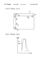
- FIG. 4 shows the measuring value of the gate voltage Vg delayed according to the length of the gate line.
- Vg 1 and Vg 2 indicate the gate voltage measured in the close point A and the far away point B of the gate line from the input terminal of the gate voltage respectively.
- the changing amount of the gate voltage becomes smaller as it becomes farther away from the input terminal of the gate voltage, that is, the delay of the gate voltage becomes larger. Accordingly, as can be known in Formula 1, the kick-back voltage ⁇ V becomes smaller.
- the waveform of the data voltage applied to the pixel electrode is distorted and accordingly the charging amount of the pixel voltage of the close point C and the far away point D from the input terminal of the data voltage becomes different.
- FIG. 5 shows the difference in the charging amount of the pixel voltage due to the delay of the data voltage.
- the data voltage is applied to the data line Dm, the voltage Vd 1 of the close point C from the input terminal becomes the data voltage Vd without a signal delay but the voltage Vd 2 of the far away point D from the input terminal does not become the data voltage Vd till it is delayed by the time constant ⁇ . Therefore, as shown with a hatched region in FIG. 5, the data voltage is less charged in the pixel of the D point than in the pixel of the C point by the ⁇ Vd.
- the difference of the charging amount affects a brightness of an image and therefore degrades the image quality. This problem becomes more serious as the panel of the LCD becomes larger.
- An object of the invention is to overcome the above described problems. Another object of the invention is to prevent the flicker due to the gate voltage delay and the ununiformity of the image due to the data voltage delay.
- FIG. 1 shows an equivalent circuit on a pixel in TFT-LCD.
- FIG. 2 shows a voltage distortion due to a kick-back voltage.
- FIG. 3 roughly shows a data line and a gate line having a resistance and a parasitic resistance on a panel of a LCD.
- FIG. 4 shows a measuring value of a gate voltage Vg delayed due to a length of the gate line.
- FIG. 5 shows a difference in charging amount of a pixel voltage due to a delay of a data voltage.
- FIG. 6 roughly shows the present invention.
- FIG. 7 shows waveforms of the data voltage and a common voltage in a point E and a point F of FIG. 6 .
- FIG. 8 roughly shows a structure of the LCD in accordance with a first embodiment of the present invention.
- FIG. 9 roughly shows a structure of the LCD in accordance with a second embodiment of the present invention.
- FIG. 10 roughly shows a structure of the LCD in accordance with a third embodiment of the present invention.
- FIG. 11 shows a driving circuit for the LCD in accordance with the first embodiment of the present invention.
- FIG. 12 shows a comparing delay means in FIG. 11 in detail.
- FIG. 13 shows a common voltage generator in FIG. 11 in detail.
- FIG. 14 shows a driving circuit for the LCD in accordance with the second embodiment of the present invention.
- the present invention applies different common voltages to the common electrode corresponding to end points of the gate line or end points of the data line.
- the smaller common voltage is applied to the common electrode close to the gate driver than the common electrode far away from the gate driver and accordingly the flicker due to the delay of the gate voltage may be prevented.
- the smaller common voltage is applied to the common electrode close to the data driver than the common electrode far away from the data driver. If the data voltage is smaller than the common voltage, the greater common voltage is applied to the common electrode close to the data driver than the common electrode far away from the data driver.
- an LCD in accordance with one aspect of the present invention comprises a first substrate which includes a plurality of the gate lines, a plurality of the data lines, a plurality of the TFTs and the pixel electrodes, and is a rectangular made up of a first edge to a fourth edge; a second substrate which includes a common electrode facing the pixel electrode; a gate pad and a data pad formed in the first edge and the second edge respectively and connected to the gate lines and the data lines respectively; a first sealant formed in the third edge for adhering the first substrate to the second substrate and having a liquid crystal injection hole for pouring the liquid crystal; a second sealant which is formed in the liquid crystal injection hole and seals the liquid crystal material after pouring the liquid crystal in; a first to a fourth common electrode points which are formed on the four edges of the common electrode and the common voltage is applied to; a dummy pad which is connected to the first, the second and the third common electrode points respectively and the different common voltages are applied to; and a common connection line
- the common connection line is formed to expose the second sealant. Further, it is preferred that the first sealant located in third edge of the first substrate is formed along with the common connection line and the corresponding part in the common connection line is formed more narrowly than the other parts.
- an LCD in accordance with the other aspect of the present invention comprises a first substrate which includes a plurality of the gate lines, a plurality of the data lines, a plurality of the TFTs and the pixel electrodes; a gate pad which is formed on the first substrate, connected to the gate line and applied a gate voltage turning on or off the TFT to; a data pad which is formed on the first substrate, connected to the data line and applied a data voltage representing an image signal to; a display area showing the image signal and comprising a set of the pixel in a matrix type defined as an intersection part between the data lines and the gate lines; a second substrate which includes a common electrode facing the pixel electrode each other; four contact points formed adjacent to four corners of the display area and having an electrical contact with the common electrode; a common voltage generator applying the different common voltages to the four contact points and the four connection lines for connecting the four contact points with the common voltage generator respectively.
- an operational amplifier is included in the connection line which connects the farthest located contact point from both the gate pad and the data pad with the common voltage generator.
- the voltage which the common voltage generator applies to the four contact points is the first highest in the farthest located contact point from both the data pad and the gate pad, the second highest in the contact point close to the data pad and far away to the gate pad, the third highest in the contact point far away from the data pad and close to the gate and the lowest in the contact point close from both the data pad and the gate pad.
- an LCD in accordance with the other aspect of the present invention comprises a first substrate which includes a plurality of the gate lines, a plurality of the data lines, a plurality of the TFTs and the pixel electrodes; a second substrate which includes a common electrode facing the pixel electrode each other; a gate driver for applying a gate voltage turning on or off the TFT to the gate line; a data driver for applying a data voltage representing an image signal to the data line; a voltage generator for applying the different common voltages to the common electrode.
- the voltage generator comprises a signal delay detector for detecting the delayed gate voltage from the gate line; a delay comparator for converting the delayed voltage detected from the signal delay detector into a digital signal; and a common voltage generator for generating the common voltage compensating the delayed voltage responsive to the digital signal input from the delay comparator.
- the voltage generator comprises a supply voltage; a first resistor having one terminal connected to the supply voltage; a first port connected the other terminal of the first resistor and a first point of the second substrate corresponding to a former part of the gate line; a second port connected to a second point of the second substrate corresponding to a latter part of the gate line; and a second resistor having one terminal connected to the second port and the other terminal grounded.
- FIG. 6 roughly shows the present invention.
- the different common voltages Vcom 1 , Vcom 2 are applied to both end points E, F of the data line and the different common voltages Vcom 3 , Vcom 4 are applied to both end points G, H of the gate line.
- the different common voltages Vcom 1 , Vcom 2 are applied to the end points E, F of the LCD panel 100 respectively and in order to prevent the flicker due to the delayed signal of the gate line, the different common voltages Vcom 3 , Vcom 4 are applied to the end points G, H respectively.
- FIG. 7 shows the waveform of the data voltage Vd(E) and the common voltage Vcom 1 applied to the end point E in FIG. 6 and the waveform of the data voltage Vd(F) and the common voltage Vcom 2 applied to the end point F.
- the common voltage Vcom 2 compensated by ⁇ V′ is applied and accordingly the voltage charging amounts of the end points E and F are made to be equal. That is, by adjusting the common voltage Vcom 2 to make ⁇ V′ and ⁇ V equal, charging amount in the pixel electrode can be equal.
- the common voltage Vcom 2 becomes the voltage lower than the common voltage Vcom 1 by ⁇ V′. If the data voltage Vd(E) (minus voltage) lower than the common voltage Vcom 1 is applied, the common voltage Vcom 2 becomes the voltage greater than the common voltage Vcom 1 by ⁇ V′.
- a data voltage compensation method to maintain the uniformity of the image can be used to a large size LCD which the data voltage is applied from an upper terminal and a lower terminal of the panel. In this case, since the data voltage is deeply distorted in a center of the panel, the common voltage for compensation is provided from the center of the panel.
- the different common voltage Vcom 3 , Vcom 4 are applied to the points G, H of the panel.
- the common voltage Vcom 4 applied to the point H is made to be greater than the common voltage Vcom 3 applied to the point G. Accordingly, each common voltage Vcom 3 , Vcom 4 can be located in a center of the pixel voltage and the flicker caused by the delayed signal of the gate line can be prevented.
- FIG. 8 roughly shows the structure of the LCD in accordance with the first embodiment of the present invention.
- the LCD in accordance with the first embodiment comprises a first substrate 110 , a second substrate 120 facing with the first substrate.
- the TFT and the pixel electrode are formed on the first substrate 110 and the first substrate is called as a TFT substrate.
- a color filter and the common electrode are formed on the second substrate 120 .
- a display area comprising a plurality of the pixels representing the image signal in a center of the two substrate 110 , 120 .
- a upper part of the exposed first substrate 110 is connected to a plurality of the data lines (are not shown) and the data pad 140 transmitting the data voltage from an external is formed.
- a left terminal of the exposed first substrate is connected to a plurality of the gate lines (are not shown) and the gate pad 150 transmitting the gate voltage from the external is formed.
- a connection parts 141 , 151 for connecting the gate line and the data line with each pad 140 , 150 are formed respectively.
- the four common electrode contact points 161 , 162 , 163 and 164 are formed in the corner exterior to the display area 130 .
- the contact points 161 , 162 , 163 and 164 receives the common voltage from the external via the dummy pads 171 , 172 , 173 formed next to the pads 140 , 150 for spare.
- the two contact points 163 , 164 formed on a right terminal of the two substrate 110 , 120 are connected to the common connection line 180 and the common connection line 180 is made of a plurality of wires composed of a low-resistance metal layer to minimize a voltage drop caused by a resistance of the common connection line.
- the different common voltages Vcom 3 , Vcom 4 are applied to the common electrode contact points 161 and 162 , 163 and 164 respectively and therefore the flicker by the delayed signal of the gate line is prevented.
- the sealant is made to be hardened by irradiating an ultra violate.
- the sealant is slow to be hardened by blocking the ultra violate irradiated to harden the sealant. Accordingly, there is a problem that the sealant not hardened completely penetrates to the display area 130 .
- FIG. 9 shows the second embodiment upgrading the structure of the LCD in accordance the first embodiment of the present invention.
- the first sealant 190 is formed around the edges of the display area 130 , the liquid crystal injection hole 196 for pouring the liquid crystal in is formed on a partial part next to a right edge of the display area 130 among the first sealant and the second sealant for sealing after pouring the liquid crystal in is formed on the liquid crystal injection hole 196 .
- the common connection line 185 is formed as different as that of the first embodiment in FIG. 8 . That is, the non-transparent metal layer is not formed on the part corresponding to the second sealant 196 and a single wire 181 is formed in a part where the second sealant is not located among parts corresponding to the liquid crystal injection hole 195 .
- the common connection line 181 is formed in a single wire, the part corresponding to the second sealant is formed in a more narrow width than other parts for not blocking the ultra violate irradiating for hardening the second sealant.
- the first sealant 190 is formed to be overlap with the common connection line 185 . Because it is good, in adjusting the interval of the two substrates 110 , 120 , that a height and a density of a pattern forming around the first substrate 110 where the first sealant is formed are made to be uniform. That is, since in the part where the first sealant overlaps among the upper part and the left terminal, the gate pad connection part 151 and the data pad connection part 152 are formed, it is preferred that the first sealant 190 is formed to overlap the common connection line 185 to have similar height and density like this in the right terminal and lower corner part of the LCD panel.
- the embodiment of the present invention shown in FIGS. 8 and 9 can prevent the flicker by making the common voltage of both ends different each other and applying to end points of the gate line.
- the ununiformity of the image can not be prevented.
- the data driver 280 for applying the data voltage is connected to a printed circuit board 272 (PCB) and in the left part of the substrate 210 , the gate driver 290 for applying the gate voltage is connected to the PCB 271 .
- the gate driver 290 and the data driver 280 are connected each to the gate line and the data line via the gate pad (is not shown) and the data pad (is not shown).
- the display area 220 where a plurality of the pixel electrodes for representing the image signal are formed in the center of the substrate 210 and the first to the fourth contact points 231 , 232 , 233 , 234 are formed in the corner of the substrate 210 .
- the four contact points 231 , 232 , 233 , 234 are connected to the common voltage generator 250 via the first to the fourth conducting wires 261 , 262 , 263 , 264 respectively.
- the common voltage generator 250 is constituted to apply the different common voltages to the conducting wires 261 , 262 , 263 , 264 .
- each conducting wire 261 , 262 , 263 , 264 is connected to the each contact point via a dummy pin (is not shown) formed as a dummy in the driver 280 , 290 through the PCB 271 , 272 .
- the conducting wire connected to the contact point 234 in the right-lower part may be formed with a repair line for repairing shorts of the data lines on the substrate 210 .
- the operational amplifier is connected to the conducting wire 264 , consequentially a short driving capability happening that the length of the conducting wire is long is compensated and a constant voltage is made to be applied to the contact point 234 formed in the right-lower part.
- the contact points 231 , 232 , 233 , 234 have contacts to the four corner of the common electrode (is not shown) formed on the upper substrate and the different common voltages which the common voltage generator 250 applies are transmitted to the common electrode.
- the different common voltages in order to prevent the ununiformity of the image caused by the delayed signal of the data line, it would be best to apply the different common voltages to both the end points of the data line in case that the data voltage is greater than the common voltage or not respectively.
- the magnitude of the common voltage generated from the common voltage generator should be change in every time.
- the greater common voltage is applied to the contact point far away from the data driver 280 than the contact point close to the data driver 280 . More specifically, the voltage applied from the common voltage generator 250 is adjusted to be raised in turn of the first contact point 231 , the second contact point 232 , in third contact point 233 and the fourth contact point 234 .
- the common electrode formed with an indium tin oxide is called as ITO
- ITO indium tin oxide
- the voltage difference between the first contact point and the fourth contact point is adjusted to keep the voltage difference between the common electrode and the pixel electrode constant in all over the display and therefore the pixel voltage turned reverse upward and downward is symmetric for the common voltage.
- FIG. 11 shows the driving circuit for the LCD in accordance with the first embodiment of the present invention.
- a controller 320 receives the images signal Vs applied to the liquid crystal from a signal source (is not shown), generates the data signal from the image signal and sends it to the data driver 330 , and makes timing signals needed in the driving circuit.
- the data driver 330 applies the data voltage to the each pixel of the LCD panel 350 according to the data signal input from the controller 320 .
- the gate driver 340 outputs the gate voltage turning on the TFT 370 in each pixel to apply the data voltage to the pixel.
- the data line 360 transmitting the data voltage from the data driver 330 and the gate line 370 which transmits the gate voltage and perpendicularly cross the data line are formed in the LCD panel 350 .
- FIG. 11 shows only an equivalent circuit on a pixel in the liquid crystal 350 .
- a voltage charged in the pixel electrode is represented as Vp and a voltage charged in the storage capacitor is represented as Vst.
- the common voltage variable generator 380 measures the gate voltage on the gate line, detects the delayed level of the gate voltage caused by the gate line and applies the common voltage to the common electrode (is not shown) of the panel 350 responsive to the delayed level.
- the common voltage variable generator 380 comprises the signal delay detector 390 , the delay comparator 392 and the common voltage generator 394 .
- the signal delay detector 390 measures the gate voltage Vg 1 , Vg 2 in the former part and the latter part of the gate line respectively. As described above, the gate voltages Vg 1 , Vg 2 have the voltage difference at a predetermined time according to the delayed signal caused by the gate line. Then, the signal delay detector 390 detects the voltage difference and transmits the detected value, a signal delay value Vgd, to the delay comparator 392 .
- the delay comparator 392 is to make the signal delay value Vgd digitized.
- FIG. 12 shows a detail circuit diagram of the delay comparator 392 .
- the delay comparator 392 comprises a serially connected plurality of the resistors R 1 , R 2 , R 3 , R 4 , and comparators 391 a , 391 b , 391 c .
- the supply voltage Vdd is made to be voltage drop by the resistors R 1 , R 2 , R 3 , R 4 and becomes reference voltages Vr 1 , Vr 2 , Vr 3 proportional to the resistance and the reference voltages Vr 1 , Vr 2 , Vr 3 become reference values of the each comparator 391 a , 391 b , 391 c .
- Each comparator 391 a , 391 b , 391 c compares the reference voltages Vr 1 , Vr 2 , Vr 3 with the signal delay value and outputs a logic signal of high or low level to output terminals Vo 1 , Vo 2 , Vo 3 .
- the signal delay value is the highest, all of the output terminals Vo 1 , Vo 2 , Vo 3 have the logic signal of high level and if the signal delay value is the smallest, all of the output terminals Vo 1 , Vo 2 , Vo 3 have the logic signal of low level.
- the output signals of the output terminals Vo 1 , Vo 2 , Vo 3 are applied to the common voltage generator 394 .
- FIG. 13 is a detailed circuit diagram of the common voltage generator 394 .
- the common voltage generator 394 comprises switches SW 1 , SW 2 and resistors R 5 , R 6 , R 7 , R 8 . According to on/off state of each switch, divided voltage of Vdd, Vcom′ is determined. The switches are turned on or off responsive to output levels of the delay comparator 392 and the Vcom′ is determined.
- the common voltage Vcom′ is applied to one point of the common electrode substrate corresponding to the latter part of the gate line which the gate signal is delayed.
- the common voltage compensating the kick-back voltage can be applied to the pixel by applying the common voltage Vcom and Vcom′ to an appropriate location of the common electrode substrate.
- the voltage difference caused by the signal delay of the gate line is measured and the common voltage is varied using the above.
- the above can be applied to the data line.
- FIG. 14 shows the LCD driving circuit in accordance with the second embodiment of the present invention.
- the second embodiment of the present invention in FIG. 14 is to replace the common voltage variable generator 380 with a common voltage generator 420 and in FIG. 14, the common voltage generator 420 mainly is shown.
- the common voltage generator 420 as shown in FIG. 14, comprises a resistor 30 having one terminal connected to the supply voltage AVDD and the other terminal coupled to a port A and a resistor 40 having one terminal connected to a port B and the other terminal grounded.
- the ports A and B are connected to the points I, J respectively.
- the internal resistance Rin of the panel is connected between the port A and the port B and the resistor R 30 , Rin, R 40 comes to be serial-connected.
- a method to generate the common voltage using the internal resistance of the panel consumes less power than a method to generate the common voltage dividing the supply voltage without using the internal resistance of the panel.
- the flicker caused by the delayed signal of the gate can be prevented. Further, by applying the different common voltages to both the end points of the data line, the ununiformity of the image quality caused by the delayed signal of the data voltage can be overcome.
Abstract
Description


Claims (19)
Applications Claiming Priority (10)
| Application Number | Priority Date | Filing Date | Title |
|---|---|---|---|
| KR1019970034423A KR19990011354A (en) | 1997-07-23 | 1997-07-23 | Driving circuit for liquid crystal display device having compensation function of common electrode voltage |
| KR97-34423 | 1997-07-23 | ||
| KR97-80208 | 1997-12-31 | ||
| KR1019970080207A KR19990059989A (en) | 1997-12-31 | 1997-12-31 | Liquid crystal display |
| KR1019970080208A KR19990059990A (en) | 1997-12-31 | 1997-12-31 | Liquid crystal display |
| KR97-80207 | 1997-12-31 | ||
| KR98-14678 | 1998-04-24 | ||
| KR1019980014678A KR19990081016A (en) | 1998-04-24 | 1998-04-24 | Liquid crystal display |
| KR1019980028547A KR100271092B1 (en) | 1997-07-23 | 1998-07-15 | A liquid crystal display having different common voltage |
| KR98-28547 | 1998-07-15 |
Publications (1)
| Publication Number | Publication Date |
|---|---|
| US6229510B1 true US6229510B1 (en) | 2001-05-08 |
Family
ID=27532238
Family Applications (1)
| Application Number | Title | Priority Date | Filing Date |
|---|---|---|---|
| US09/120,949 Expired - Lifetime US6229510B1 (en) | 1997-07-23 | 1998-07-22 | Liquid crystal display having different common voltages |
Country Status (4)
| Country | Link |
|---|---|
| US (1) | US6229510B1 (en) |
| JP (1) | JP3656940B2 (en) |
| KR (1) | KR100271092B1 (en) |
| TW (1) | TW505814B (en) |
Cited By (40)
| Publication number | Priority date | Publication date | Assignee | Title |
|---|---|---|---|---|
| US20020024484A1 (en) * | 1999-11-18 | 2002-02-28 | Gyu-Su Lee | Liquid crystal display device |
| US6392626B1 (en) * | 1998-11-06 | 2002-05-21 | Samsung Electronics Co., Ltd. | Liquid crystal display having different common voltages |
| US6567064B1 (en) * | 1999-09-21 | 2003-05-20 | Lg. Philips Lcd Co., Ltd. | Liquid crystal display device |
| US20030117353A1 (en) * | 2001-11-26 | 2003-06-26 | Moon Seung Hwan | Liquid crystal display and driving method thereof |
| WO2003052500A1 (en) * | 2001-12-17 | 2003-06-26 | Rainbow Displays, Inc. | Construction of large, robust, monolithic and monolithic-like, amlcd displays with wide view angle |
| US20030117566A1 (en) * | 2001-12-22 | 2003-06-26 | Park Jung Sik | Liquid crystal display of line-on-glass type |
| US6590552B1 (en) * | 1998-06-29 | 2003-07-08 | Sanyo Electric Co., Ltd. | Method of driving liquid crystal display device |
| US20030184703A1 (en) * | 2000-01-21 | 2003-10-02 | Greene Raymond G. | Construction of large, robust, monolithic and monolithic-like, AMLCD displays with wide view angle |
| US6646691B1 (en) * | 1999-07-26 | 2003-11-11 | Nec Lcd Technologies, Ltd. | Active-matrix in-plane switching mode LCD panel having multiple common electrode voltage sources |
| US6653999B2 (en) * | 1998-12-15 | 2003-11-25 | Sanyo Electric Co., Ltd. | Integrated circuit for driving liquid crystal |
| US6670936B1 (en) * | 1998-01-09 | 2003-12-30 | Hitachi, Ltd. | Liquid crystal display |
| US20040046724A1 (en) * | 2002-09-06 | 2004-03-11 | Lg.Philips Lcd Co., Ltd And A Pto | Signal driving circuit of liquid crystal display device and driving method thereof |
| WO2005006287A1 (en) * | 2003-07-15 | 2005-01-20 | Koninklijke Philips Electronics N.V. | Active matrix display |
| US20050184979A1 (en) * | 2004-02-19 | 2005-08-25 | Nobuhisa Sakaguchi | Liquid crystal display device |
| US20060066553A1 (en) * | 2002-12-19 | 2006-03-30 | Koninklijke Philips Electronics N.V. | Active matrix display device with dc voltage compensation based on measurements on a plurality of measurement pixels outside the display area |
| US7050027B1 (en) | 2004-01-16 | 2006-05-23 | Maxim Integrated Products, Inc. | Single wire interface for LCD calibrator |
| US20060192738A1 (en) * | 2001-09-27 | 2006-08-31 | Tetsuya Kawamura | Liquid crystal display device and manufacturing method thereof |
| US20070146276A1 (en) * | 2005-12-23 | 2007-06-28 | Innolux Display Corp. | Active matrix liquid crystal display and driving method thereof |
| US20070152943A1 (en) * | 2005-12-29 | 2007-07-05 | Kwang Hee Hwang | Liquid crystal display device |
| US20080252584A1 (en) * | 2007-04-10 | 2008-10-16 | Hitachi Displays, Ltd. | Liquid crystal display device |
| US20080259068A1 (en) * | 2007-04-18 | 2008-10-23 | Au Optronics Corp. | Display panel and electro-optical apparatus |
| US20080284966A1 (en) * | 2002-10-30 | 2008-11-20 | Ryouichi Ootsu | Image Display Device |
| US20080291144A1 (en) * | 2007-05-25 | 2008-11-27 | Innolux Display Corp. | Liquid crystal display having common voltage modulator |
| US20090096735A1 (en) * | 2007-10-12 | 2009-04-16 | Innocom Technology (Shenzhen) Co., Ltd. | Liquid crystal display having compensation circuit for reducing gate delay |
| US20090135361A1 (en) * | 2006-02-22 | 2009-05-28 | Ruibo Lu | Systems for Displaying Images Involving Alignment Liquid Crystal Displays |
| CN101398584B (en) * | 2007-09-27 | 2010-08-11 | 北京京东方光电科技有限公司 | Method for driving LCD device |
| US20100245306A1 (en) * | 2000-05-12 | 2010-09-30 | Semiconductor Energy Laboratory Co., Ltd. | Semiconductor device |
| US20100245326A1 (en) * | 2009-03-25 | 2010-09-30 | Beijing Boe Optoelectronics Technology Co., Ltd. | Common electrode drive circuit and liquid crystal display |
| US20120242641A1 (en) * | 2011-03-24 | 2012-09-27 | Kwangsae Lee | Display device and method of operating the same |
| WO2012140434A1 (en) * | 2011-04-14 | 2012-10-18 | Plastic Logic Limited | Display systems |
| TWI408653B (en) * | 2008-11-05 | 2013-09-11 | Himax Display Inc | Setting method and setting system for setting a common voltage of an lcd device thereof |
| US20130302921A1 (en) * | 2012-05-09 | 2013-11-14 | Seiko Epson Corporation | Method for producing electro-optical device and substrate for electro-optical device |
| US20130307761A1 (en) * | 2012-05-16 | 2013-11-21 | Samsung Display Co., Ltd. | Display device |
| US20150077409A1 (en) * | 2011-10-05 | 2015-03-19 | Au Optronics Corp. | Liquid crystal display having adaptive pulse shaping control mechanism |
| US9013383B2 (en) | 2009-11-26 | 2015-04-21 | David Hough | Display systems |
| CN104777942A (en) * | 2015-05-08 | 2015-07-15 | 厦门天马微电子有限公司 | Touch control display panel, driving method and touch control display device |
| US20160196775A1 (en) * | 2015-01-07 | 2016-07-07 | Samsung Display Co., Ltd. | Display device |
| TWI620164B (en) * | 2013-05-17 | 2018-04-01 | 達樂股份有限公司 | Electro-optical device with large pixel matrix |
| CN108198540A (en) * | 2018-02-26 | 2018-06-22 | 惠科股份有限公司 | The driving method and system of a kind of display device |
| CN114660859A (en) * | 2022-03-16 | 2022-06-24 | Tcl华星光电技术有限公司 | Display panel and display device |
Families Citing this family (17)
| Publication number | Priority date | Publication date | Assignee | Title |
|---|---|---|---|---|
| US6721029B2 (en) * | 1999-08-23 | 2004-04-13 | Agilent Technologies, Inc. | Electro-optical material-based display device |
| KR100709701B1 (en) * | 1999-12-01 | 2007-04-19 | 삼성전자주식회사 | A liquid crystal display having different common voltages |
| KR20020071995A (en) * | 2001-03-08 | 2002-09-14 | 삼성전자 주식회사 | liquid crystal device for compensating kick-back voltage |
| JP3845551B2 (en) | 2001-04-19 | 2006-11-15 | セイコーエプソン株式会社 | ELECTRODE DRIVE DEVICE AND ELECTRONIC DEVICE |
| KR100729769B1 (en) * | 2001-06-18 | 2007-06-20 | 삼성전자주식회사 | Liquid crystal display |
| JP2003162262A (en) * | 2001-11-27 | 2003-06-06 | Fujitsu Display Technologies Corp | Liquid crystal panel driving circuit and liquid crystal display device |
| KR20030058117A (en) * | 2001-12-29 | 2003-07-07 | 엘지.필립스 엘시디 주식회사 | Protection circuit for Liquid crystal display device |
| KR100917008B1 (en) * | 2003-06-10 | 2009-09-10 | 삼성전자주식회사 | Liquid crystal display device |
| KR101127847B1 (en) * | 2005-06-28 | 2012-03-21 | 엘지디스플레이 주식회사 | Liquid crystal display of line on glass type |
| KR101168886B1 (en) * | 2005-12-12 | 2012-07-30 | 엘지디스플레이 주식회사 | Liquid crystal displau divece for preventing delay of common signal |
| JP4975322B2 (en) * | 2005-12-28 | 2012-07-11 | ティーピーオー、ホンコン、ホールディング、リミテッド | Active matrix liquid crystal display device and control method thereof |
| KR101225317B1 (en) * | 2005-12-28 | 2013-01-22 | 엘지디스플레이 주식회사 | Apparatus and method for driving LCD |
| JP5026738B2 (en) * | 2006-05-31 | 2012-09-19 | 株式会社ジャパンディスプレイイースト | Display device |
| JP4400605B2 (en) * | 2006-09-25 | 2010-01-20 | カシオ計算機株式会社 | Display driving device and display device |
| TWI386901B (en) * | 2008-03-14 | 2013-02-21 | Chimei Innolux Corp | Lcd and driving method thereof |
| KR102222195B1 (en) * | 2014-12-24 | 2021-03-05 | 엘지디스플레이 주식회사 | Display device, gate signal sensing circuit and data driver |
| CN115236906B (en) * | 2022-06-30 | 2023-08-22 | 苏州华星光电技术有限公司 | display device |
Citations (6)
| Publication number | Priority date | Publication date | Assignee | Title |
|---|---|---|---|---|
| JPH05341732A (en) | 1992-06-05 | 1993-12-24 | Fujitsu Ltd | Active matrix type liquid crystal display device |
| JPH06161390A (en) | 1992-11-26 | 1994-06-07 | Kyocera Corp | Method for driving liquid crystal display device |
| US5774099A (en) * | 1995-04-25 | 1998-06-30 | Hitachi, Ltd. | Liquid crystal device with wide viewing angle characteristics |
| US5798741A (en) * | 1994-12-28 | 1998-08-25 | Sharp Kabushiki Kaisha | Power source for driving liquid crystal |
| US6005542A (en) * | 1996-03-30 | 1999-12-21 | Lg Electronics Inc. | Method for driving a thin film transistor liquid crystal display device using varied gate low levels |
| US6052104A (en) * | 1995-07-12 | 2000-04-18 | Lg Electronics Inc. | Structure and operation method of LCD |
-
1998
- 1998-07-15 KR KR1019980028547A patent/KR100271092B1/en not_active IP Right Cessation
- 1998-07-22 US US09/120,949 patent/US6229510B1/en not_active Expired - Lifetime
- 1998-07-23 JP JP20783898A patent/JP3656940B2/en not_active Expired - Fee Related
- 1998-07-23 TW TW087112043A patent/TW505814B/en not_active IP Right Cessation
Patent Citations (6)
| Publication number | Priority date | Publication date | Assignee | Title |
|---|---|---|---|---|
| JPH05341732A (en) | 1992-06-05 | 1993-12-24 | Fujitsu Ltd | Active matrix type liquid crystal display device |
| JPH06161390A (en) | 1992-11-26 | 1994-06-07 | Kyocera Corp | Method for driving liquid crystal display device |
| US5798741A (en) * | 1994-12-28 | 1998-08-25 | Sharp Kabushiki Kaisha | Power source for driving liquid crystal |
| US5774099A (en) * | 1995-04-25 | 1998-06-30 | Hitachi, Ltd. | Liquid crystal device with wide viewing angle characteristics |
| US6052104A (en) * | 1995-07-12 | 2000-04-18 | Lg Electronics Inc. | Structure and operation method of LCD |
| US6005542A (en) * | 1996-03-30 | 1999-12-21 | Lg Electronics Inc. | Method for driving a thin film transistor liquid crystal display device using varied gate low levels |
Cited By (77)
| Publication number | Priority date | Publication date | Assignee | Title |
|---|---|---|---|---|
| US6670936B1 (en) * | 1998-01-09 | 2003-12-30 | Hitachi, Ltd. | Liquid crystal display |
| US6590552B1 (en) * | 1998-06-29 | 2003-07-08 | Sanyo Electric Co., Ltd. | Method of driving liquid crystal display device |
| US6392626B1 (en) * | 1998-11-06 | 2002-05-21 | Samsung Electronics Co., Ltd. | Liquid crystal display having different common voltages |
| US6653999B2 (en) * | 1998-12-15 | 2003-11-25 | Sanyo Electric Co., Ltd. | Integrated circuit for driving liquid crystal |
| US6646691B1 (en) * | 1999-07-26 | 2003-11-11 | Nec Lcd Technologies, Ltd. | Active-matrix in-plane switching mode LCD panel having multiple common electrode voltage sources |
| US6693684B2 (en) * | 1999-09-15 | 2004-02-17 | Rainbow Displays, Inc. | Construction of large, robust, monolithic and monolithic-like, AMLCD displays with wide view angle |
| US6567064B1 (en) * | 1999-09-21 | 2003-05-20 | Lg. Philips Lcd Co., Ltd. | Liquid crystal display device |
| US20020024484A1 (en) * | 1999-11-18 | 2002-02-28 | Gyu-Su Lee | Liquid crystal display device |
| US6822632B2 (en) * | 1999-11-18 | 2004-11-23 | Samsung Electronics Co., Ltd. | Liquid crystal display device |
| US20030184703A1 (en) * | 2000-01-21 | 2003-10-02 | Greene Raymond G. | Construction of large, robust, monolithic and monolithic-like, AMLCD displays with wide view angle |
| US7995024B2 (en) * | 2000-05-12 | 2011-08-09 | Semiconductor Energy Laboratory Co., Ltd. | Semiconductor device |
| US8564578B2 (en) | 2000-05-12 | 2013-10-22 | Semiconductor Energy Laboratory Co., Ltd. | Semiconductor device |
| US20100245306A1 (en) * | 2000-05-12 | 2010-09-30 | Semiconductor Energy Laboratory Co., Ltd. | Semiconductor device |
| US20060192738A1 (en) * | 2001-09-27 | 2006-08-31 | Tetsuya Kawamura | Liquid crystal display device and manufacturing method thereof |
| US7796105B2 (en) * | 2001-11-26 | 2010-09-14 | Samsung Electronics Co., Ltd. | Liquid crystal display and driving method thereof |
| US20110227902A1 (en) * | 2001-11-26 | 2011-09-22 | Samsung Electronics Co., Ltd. | Liquid crystal display and driving method thereof |
| US20060187173A1 (en) * | 2001-11-26 | 2006-08-24 | Moon Seung H | Liquid crystal display and driving method thereof |
| US7209102B2 (en) * | 2001-11-26 | 2007-04-24 | Samsung Electronics Co., Ltd. | Liquid crystal display and driving method thereof |
| US20030117353A1 (en) * | 2001-11-26 | 2003-06-26 | Moon Seung Hwan | Liquid crystal display and driving method thereof |
| US20070152940A1 (en) * | 2001-11-26 | 2007-07-05 | Samsung Electronics Co., Ltd. | Liquid crystal display and driving method thereof |
| US8692819B2 (en) | 2001-11-26 | 2014-04-08 | Samsung Display Co., Ltd. | Liquid crystal display having different reference voltages applied to reference electrode |
| WO2003052500A1 (en) * | 2001-12-17 | 2003-06-26 | Rainbow Displays, Inc. | Construction of large, robust, monolithic and monolithic-like, amlcd displays with wide view angle |
| US7705820B2 (en) * | 2001-12-22 | 2010-04-27 | Lg Display Co., Ltd. | Liquid crystal display of line-on-glass type |
| US20030117566A1 (en) * | 2001-12-22 | 2003-06-26 | Park Jung Sik | Liquid crystal display of line-on-glass type |
| US8581820B2 (en) * | 2002-09-06 | 2013-11-12 | Lg Display Co., Ltd. | Signal driving circuit of liquid crystal display device and driving method thereof |
| US9024856B2 (en) | 2002-09-06 | 2015-05-05 | Lg Display Co., Ltd. | Signal driving circuit of liquid crystal display device and driving method thereof |
| US20040046724A1 (en) * | 2002-09-06 | 2004-03-11 | Lg.Philips Lcd Co., Ltd And A Pto | Signal driving circuit of liquid crystal display device and driving method thereof |
| US8089439B2 (en) * | 2002-10-30 | 2012-01-03 | Hitachi Displays, Ltd. | Image display device |
| US20080284966A1 (en) * | 2002-10-30 | 2008-11-20 | Ryouichi Ootsu | Image Display Device |
| US20060066553A1 (en) * | 2002-12-19 | 2006-03-30 | Koninklijke Philips Electronics N.V. | Active matrix display device with dc voltage compensation based on measurements on a plurality of measurement pixels outside the display area |
| WO2005006287A1 (en) * | 2003-07-15 | 2005-01-20 | Koninklijke Philips Electronics N.V. | Active matrix display |
| US7050027B1 (en) | 2004-01-16 | 2006-05-23 | Maxim Integrated Products, Inc. | Single wire interface for LCD calibrator |
| US20050184979A1 (en) * | 2004-02-19 | 2005-08-25 | Nobuhisa Sakaguchi | Liquid crystal display device |
| US7834837B2 (en) * | 2005-12-23 | 2010-11-16 | Chimei Innolux Corporation | Active matrix liquid crystal display and driving method thereof |
| US20070146276A1 (en) * | 2005-12-23 | 2007-06-28 | Innolux Display Corp. | Active matrix liquid crystal display and driving method thereof |
| US8416164B2 (en) * | 2005-12-29 | 2013-04-09 | Lg Display Co., Ltd. | Liquid crystal display device |
| DE102006026500B4 (en) * | 2005-12-29 | 2009-11-26 | Lg Display Co., Ltd. | Liquid crystal display device |
| US20070152943A1 (en) * | 2005-12-29 | 2007-07-05 | Kwang Hee Hwang | Liquid crystal display device |
| DE102006026500B8 (en) * | 2005-12-29 | 2010-03-04 | Lg Display Co., Ltd. | Liquid crystal display device |
| GB2434021A (en) * | 2005-12-29 | 2007-07-11 | Lg Philips Lcd Co Ltd | Liquid crystal display device having first and second common voltage supply lines |
| GB2434021B (en) * | 2005-12-29 | 2008-02-27 | Lg Philips Lcd Co Ltd | Liquid crystal display device |
| US20090135361A1 (en) * | 2006-02-22 | 2009-05-28 | Ruibo Lu | Systems for Displaying Images Involving Alignment Liquid Crystal Displays |
| US20080252584A1 (en) * | 2007-04-10 | 2008-10-16 | Hitachi Displays, Ltd. | Liquid crystal display device |
| US20080259068A1 (en) * | 2007-04-18 | 2008-10-23 | Au Optronics Corp. | Display panel and electro-optical apparatus |
| US8462094B2 (en) | 2007-04-18 | 2013-06-11 | Au Optronics Corp. | Display panel including a cascade driver and opto-electronic apparatus thereof |
| US20080291144A1 (en) * | 2007-05-25 | 2008-11-27 | Innolux Display Corp. | Liquid crystal display having common voltage modulator |
| US8199092B2 (en) | 2007-05-25 | 2012-06-12 | Chimei Innolux Corporation | Liquid crystal display having common voltage modulator |
| CN101398584B (en) * | 2007-09-27 | 2010-08-11 | 北京京东方光电科技有限公司 | Method for driving LCD device |
| US20090096735A1 (en) * | 2007-10-12 | 2009-04-16 | Innocom Technology (Shenzhen) Co., Ltd. | Liquid crystal display having compensation circuit for reducing gate delay |
| US8217926B2 (en) * | 2007-10-12 | 2012-07-10 | Innocom Technology (Shenzhen) Co., Ltd. | Liquid crystal display having compensation circuit for reducing gate delay |
| TWI408653B (en) * | 2008-11-05 | 2013-09-11 | Himax Display Inc | Setting method and setting system for setting a common voltage of an lcd device thereof |
| US8878829B2 (en) * | 2009-03-25 | 2014-11-04 | Beijing Boe Optoelectronics Technology Co., Ltd. | Liquid crystal display and common electrode drive circuit thereof |
| US20100245326A1 (en) * | 2009-03-25 | 2010-09-30 | Beijing Boe Optoelectronics Technology Co., Ltd. | Common electrode drive circuit and liquid crystal display |
| CN101847376B (en) * | 2009-03-25 | 2013-10-30 | 北京京东方光电科技有限公司 | Common electrode driving circuit and LCD |
| US9013383B2 (en) | 2009-11-26 | 2015-04-21 | David Hough | Display systems |
| US20120242641A1 (en) * | 2011-03-24 | 2012-09-27 | Kwangsae Lee | Display device and method of operating the same |
| US8988410B2 (en) * | 2011-03-24 | 2015-03-24 | Samsung Display Co., Ltd. | Display device and method of operating the same |
| US9336731B2 (en) | 2011-04-14 | 2016-05-10 | Flexenable Limited | System and method to compensate for an induced voltage on a pixel drive electrode |
| WO2012140434A1 (en) * | 2011-04-14 | 2012-10-18 | Plastic Logic Limited | Display systems |
| US20150077409A1 (en) * | 2011-10-05 | 2015-03-19 | Au Optronics Corp. | Liquid crystal display having adaptive pulse shaping control mechanism |
| US9881573B2 (en) * | 2011-10-05 | 2018-01-30 | Au Optronics Corp. | Liquid crystal display having adaptive pulse shaping control mechanism |
| US8865491B2 (en) * | 2012-05-09 | 2014-10-21 | Seiko Epson Corporation | Method for producing electro-optical device and substrate for electro-optical device |
| US20130302921A1 (en) * | 2012-05-09 | 2013-11-14 | Seiko Epson Corporation | Method for producing electro-optical device and substrate for electro-optical device |
| US20130307761A1 (en) * | 2012-05-16 | 2013-11-21 | Samsung Display Co., Ltd. | Display device |
| US10332473B2 (en) | 2012-05-16 | 2019-06-25 | Samsung Display Co., Ltd. | Display device |
| US9626930B2 (en) * | 2012-05-16 | 2017-04-18 | Samsung Display Co., Ltd. | Display device |
| TWI620164B (en) * | 2013-05-17 | 2018-04-01 | 達樂股份有限公司 | Electro-optical device with large pixel matrix |
| US9767722B2 (en) * | 2015-01-07 | 2017-09-19 | Samsung Display Co., Ltd. | Display device |
| US20160196775A1 (en) * | 2015-01-07 | 2016-07-07 | Samsung Display Co., Ltd. | Display device |
| CN104777942A (en) * | 2015-05-08 | 2015-07-15 | 厦门天马微电子有限公司 | Touch control display panel, driving method and touch control display device |
| CN104777942B (en) * | 2015-05-08 | 2018-02-06 | 厦门天马微电子有限公司 | Touch-control display panel, driving method and touch control display apparatus |
| US20160328075A1 (en) * | 2015-05-08 | 2016-11-10 | Xiamen Tianma Micro-Electronics Co., Ltd. | Touch display panel, driving method and touch display device |
| US10620738B2 (en) * | 2015-05-08 | 2020-04-14 | Xiamen Tianma Micro-Electronics Co., Ltd. | Touch display panel, driving method and touch display device |
| CN108198540A (en) * | 2018-02-26 | 2018-06-22 | 惠科股份有限公司 | The driving method and system of a kind of display device |
| CN108198540B (en) * | 2018-02-26 | 2019-12-13 | 惠科股份有限公司 | Driving method and system of display device |
| CN114660859A (en) * | 2022-03-16 | 2022-06-24 | Tcl华星光电技术有限公司 | Display panel and display device |
| CN114660859B (en) * | 2022-03-16 | 2023-07-04 | Tcl华星光电技术有限公司 | Display panel and display device |
Also Published As
| Publication number | Publication date |
|---|---|
| TW505814B (en) | 2002-10-11 |
| KR100271092B1 (en) | 2000-11-01 |
| JPH11133379A (en) | 1999-05-21 |
| JP3656940B2 (en) | 2005-06-08 |
| KR19990013875A (en) | 1999-02-25 |
Similar Documents
| Publication | Publication Date | Title |
|---|---|---|
| US6229510B1 (en) | Liquid crystal display having different common voltages | |
| US7786960B2 (en) | Liquid crystal display and driving method thereof | |
| KR0163938B1 (en) | Driving circuit of thin film transistor liquid crystal device | |
| US6246385B1 (en) | Liquid crystal display device and its driving method | |
| US8878829B2 (en) | Liquid crystal display and common electrode drive circuit thereof | |
| US7898514B2 (en) | Apparatus for driving gate of liquid crystal display and driving method thereof | |
| US7705820B2 (en) | Liquid crystal display of line-on-glass type | |
| US6714182B2 (en) | Method and system of compensating kickback voltage for a liquid crystal display device | |
| US7091966B2 (en) | Electro-optical device, drive device and drive method for electro-optical device, and electronic apparatus | |
| US7427739B2 (en) | Electro-optical device and electronic apparatus | |
| US8054265B2 (en) | Liquid crystal display apparatus and driving method thereof | |
| US7834831B2 (en) | Liquid crystal display device and method for driving the same | |
| KR100612991B1 (en) | Liquid crystal display | |
| US7643121B2 (en) | Liquid crystal display of line-on-glass type | |
| JP4326242B2 (en) | Liquid crystal display | |
| TWI418882B (en) | Liquid crystal display capable of switching the common voltage | |
| KR101135947B1 (en) | Liquid crystal display | |
| KR100675925B1 (en) | Liquid crystal display for diminishing flicker from controlling delay of gate signal | |
| KR100978255B1 (en) | Liquid crystal display device and driving method thereof | |
| US6842203B2 (en) | Liquid crystal display of line-on-glass type | |
| KR20050001063A (en) | Liquid crystal display device | |
| KR20060022498A (en) | Display device | |
| KR100879214B1 (en) | Liquid crystal display device | |
| KR20030073074A (en) | Method for driving liquid crystal display device and circuit thereof | |
| KR20040002290A (en) | Liquid crystal display device of line on glass type and method of fabricating the same |
Legal Events
| Date | Code | Title | Description |
|---|---|---|---|
| AS | Assignment |
Owner name: SAMSUNG ELECTRONICS CO., LTD., KOREA, REPUBLIC OF Free format text: ASSIGNMENT OF ASSIGNORS INTEREST;ASSIGNORS:KIM, WAN-BAE;LEE, SEUNG-JUN;YOU, BONG-HYUN;AND OTHERS;REEL/FRAME:009439/0805 Effective date: 19980720 |
|
| STCF | Information on status: patent grant |
Free format text: PATENTED CASE |
|
| FEPP | Fee payment procedure |
Free format text: PAYOR NUMBER ASSIGNED (ORIGINAL EVENT CODE: ASPN); ENTITY STATUS OF PATENT OWNER: LARGE ENTITY |
|
| FPAY | Fee payment |
Year of fee payment: 4 |
|
| FPAY | Fee payment |
Year of fee payment: 8 |
|
| FEPP | Fee payment procedure |
Free format text: PAYER NUMBER DE-ASSIGNED (ORIGINAL EVENT CODE: RMPN); ENTITY STATUS OF PATENT OWNER: LARGE ENTITY Free format text: PAYOR NUMBER ASSIGNED (ORIGINAL EVENT CODE: ASPN); ENTITY STATUS OF PATENT OWNER: LARGE ENTITY |
|
| AS | Assignment |
Owner name: SAMSUNG DISPLAY CO., LTD., KOREA, REPUBLIC OF Free format text: ASSIGNMENT OF ASSIGNORS INTEREST;ASSIGNOR:SAMSUNG ELECTRONICS CO., LTD.;REEL/FRAME:028984/0774 Effective date: 20120904 |
|
| FPAY | Fee payment |
Year of fee payment: 12 |