US6233193B1 - Dynamic random access memory system with a static random access memory interface and methods for using the same - Google Patents
Dynamic random access memory system with a static random access memory interface and methods for using the same Download PDFInfo
- Publication number
- US6233193B1 US6233193B1 US09/295,641 US29564199A US6233193B1 US 6233193 B1 US6233193 B1 US 6233193B1 US 29564199 A US29564199 A US 29564199A US 6233193 B1 US6233193 B1 US 6233193B1
- Authority
- US
- United States
- Prior art keywords
- refresh
- address
- access
- row
- cell
- Prior art date
- Legal status (The legal status is an assumption and is not a legal conclusion. Google has not performed a legal analysis and makes no representation as to the accuracy of the status listed.)
- Expired - Lifetime
Links
- 238000000034 method Methods 0.000 title claims description 30
- 230000003068 static effect Effects 0.000 title description 4
- 230000015654 memory Effects 0.000 claims abstract description 104
- 230000004044 response Effects 0.000 claims abstract description 43
- 239000003990 capacitor Substances 0.000 claims description 36
- 238000003860 storage Methods 0.000 claims description 27
- 230000008878 coupling Effects 0.000 claims description 13
- 238000010168 coupling process Methods 0.000 claims description 13
- 238000005859 coupling reaction Methods 0.000 claims description 13
- 238000001514 detection method Methods 0.000 claims description 6
- 230000004913 activation Effects 0.000 claims description 4
- 238000013500 data storage Methods 0.000 claims description 3
- 230000005669 field effect Effects 0.000 claims 3
- 230000003213 activating effect Effects 0.000 claims 1
- 238000010586 diagram Methods 0.000 description 20
- 230000008569 process Effects 0.000 description 13
- 239000000758 substrate Substances 0.000 description 11
- 230000002093 peripheral effect Effects 0.000 description 10
- 230000008901 benefit Effects 0.000 description 9
- 239000000872 buffer Substances 0.000 description 9
- 230000000630 rising effect Effects 0.000 description 8
- 230000001360 synchronised effect Effects 0.000 description 7
- 230000007704 transition Effects 0.000 description 7
- 239000003989 dielectric material Substances 0.000 description 6
- 230000006870 function Effects 0.000 description 6
- 238000004519 manufacturing process Methods 0.000 description 6
- 238000005516 engineering process Methods 0.000 description 5
- 238000013461 design Methods 0.000 description 4
- 239000000463 material Substances 0.000 description 4
- 238000012545 processing Methods 0.000 description 4
- 230000008859 change Effects 0.000 description 3
- 230000000295 complement effect Effects 0.000 description 3
- 238000010276 construction Methods 0.000 description 3
- 238000013459 approach Methods 0.000 description 2
- 238000002955 isolation Methods 0.000 description 2
- 238000007726 management method Methods 0.000 description 2
- 230000007246 mechanism Effects 0.000 description 2
- 238000012986 modification Methods 0.000 description 2
- 230000004048 modification Effects 0.000 description 2
- 239000004065 semiconductor Substances 0.000 description 2
- 240000007320 Pinus strobus Species 0.000 description 1
- 238000003491 array Methods 0.000 description 1
- 230000009172 bursting Effects 0.000 description 1
- 230000003111 delayed effect Effects 0.000 description 1
- 238000009826 distribution Methods 0.000 description 1
- 230000008030 elimination Effects 0.000 description 1
- 238000003379 elimination reaction Methods 0.000 description 1
- 230000000977 initiatory effect Effects 0.000 description 1
- 230000003993 interaction Effects 0.000 description 1
- 230000014759 maintenance of location Effects 0.000 description 1
- 239000011159 matrix material Substances 0.000 description 1
- 238000004806 packaging method and process Methods 0.000 description 1
- 230000000737 periodic effect Effects 0.000 description 1
- 238000000638 solvent extraction Methods 0.000 description 1
- 238000012546 transfer Methods 0.000 description 1
Images


Classifications
-
- G—PHYSICS
- G11—INFORMATION STORAGE
- G11C—STATIC STORES
- G11C7/00—Arrangements for writing information into, or reading information out from, a digital store
-
- G—PHYSICS
- G11—INFORMATION STORAGE
- G11C—STATIC STORES
- G11C11/00—Digital stores characterised by the use of particular electric or magnetic storage elements; Storage elements therefor
- G11C11/21—Digital stores characterised by the use of particular electric or magnetic storage elements; Storage elements therefor using electric elements
- G11C11/34—Digital stores characterised by the use of particular electric or magnetic storage elements; Storage elements therefor using electric elements using semiconductor devices
- G11C11/40—Digital stores characterised by the use of particular electric or magnetic storage elements; Storage elements therefor using electric elements using semiconductor devices using transistors
- G11C11/401—Digital stores characterised by the use of particular electric or magnetic storage elements; Storage elements therefor using electric elements using semiconductor devices using transistors forming cells needing refreshing or charge regeneration, i.e. dynamic cells
- G11C11/406—Management or control of the refreshing or charge-regeneration cycles
Definitions
- the present invention relates in general to electronic memories and in particular to a dynamic random access memory with a Static Random Access Memory Interface operations and methods using the same.
- Dynamic random access memory is the principal type of memory used in most applications such as personal computers (PCS). When compared, for example, to static random access memory (SRAM), DRAM is less expensive, consumes substantially less power, and provides more bits in the same chip space (i.e. has a higher cell density). DRAM is normally used to construct those memory subsystems, such as system memories and display frame buffers, where power conservation and high cell density are more critical than speed. In most computing systems, it is these subsystems which dominate the system architecture, thus making DRAM the prevalent type of memory device on the market.
- SRAM static random access memory
- DRAMs are also subject to significant restraints due to the manner in which they must be constructed and operated. Specifically, since each cell stores data as charge on a capacitor (i.e. charged to a predetermined voltage for a logic 1 and discharged to approximately 0 volts for a logic 0), the length of time a bit, and in particular a logic 1 bit, can be stored in a given cell is a function of the ability of the capacitor to retain charge. Charge retention, and consequently data integrity is in turn a function of charge leakage.
- Efforts have been made to minimize cell leakage such that the integrity of the data can be maintained for a longer period of time and hence the period between required refresh correspondingly increased.
- One way has been to bias the substrate in which the cells sit to reduce subthreshold leakage.
- a triple-well process is used.
- the n-channel pass transistors in the DRAM cell (as well as the storage capacitors) array sit in an isolated p-type well which in turn sits in a n-type well.
- the n-type well has previously been formed in a p-type substrate.
- V BB negative voltage
- Ip-channel pass transistors sit in an isolated n-type well which in turn sits in an s-type well. This effectively raises the threshold voltage of the cell pass transistors and cuts off subthreshold leakage.
- the separate p-well is used to isolate the array from the peripherals such that the biasing of the cell array does not degrade the performance of the peripheral circuits which have a grounded substrate. Without the isolated p-well, the substrate biasing would also raise the threshold of the transistors in the high performance peripherals and deteriorate their performance.
- Capacitor size is a function of the capacitor dielectric material chosen, the higher the dielectric constant of the material, the more capacitance can be achieved per unit area. While high dielectric materials allow for the fabrication of smaller capacitors, such materials, due to their physical nature, are leaky and must be refreshed at a higher rate. On the other hand, lower dielectric materials are less leaky but force the use of larger capacitor plates. As a consequence, trench, stacked and other complex capacitor structures have been developed to allow the use of lower dielectric constant, lower leakage materials, and which consequently increase in capacitor plate size, while still allowing the overall size of the cells to be small.
- circuits, system and methods which support efficient refresh of DRAM arrays.
- Such methods circuits, systems and methods should be sufficiently robust such that the triple-well process and the associated charge pumps can be eliminated. Further, the ability to use leaky, high dielectric materials in the construction of smaller memory cells should also be addressed.
- a memory comprising an array of rows and columns of dynamic memory cells, the cells of each of the rows coupled to an access wordline and a refresh wordline and the cells of each column coupled to an access bitline and refresh bitline.
- Refresh circuitry refreshes a row of cells using a corresponding refresh wordline and a corresponding refresh bitline.
- Access circuitry accesses selected cells of a selected row using a corresponding access wordline and a corresponding access bitline.
- the access circuitry includes a new address detector for detecting receipt of a new address by the memory, a row decoder for selecting the access wordline in response to receipt of the row address, and access sense amplifiers and an access column decoder accessing at least one cell along the selected access wordline using the corresponding access bitline.
- the present concepts are also embodied in an information storage device.
- a plurality of memory cells are organized in rows and columns, with each cell including a first transistor for coupling a storage capacitor of the cell with a first data line of a column of cells in response to a signal applied to a first control line to a row of cells containing the cell and a second transistor for coupling the capacitor with the second data line of the column of cells in response to a signal applied via a second control line to a row of cells containing the cell.
- the device also includes access circuitry and refresh circuitry.
- the access circuitry generates the receipt of an access address addressing a cell being accessed, decodes the address to activate the first control line of the row containing the cell being accessed, and exchanges data with that cell via the first data line of the column containing that cell.
- the refresh circuitry generates a refresh address addressing a cell being refreshed, compares the refresh address with the access address, and when the refresh address and the access address do not match, refreshes the cell being refreshed via the second control line of the row containing the cell.
- a further embodiment of the present teachings is a memory system which includes a plurality of blocks of data storage circuitry.
- Each block includes a subarray of 2-transistor, 1-capacitor memory cells disposed in rows and columns, first transistor of each cell selectively coupling a cell storage capacitor with a first bitline of a corresponding column in response to activation of a first subwordline of a corresponding row and a second transistor of each cell selectively coupling the cell storage capacitor with a second bitline of the corresponding column in response to activation of a second subwordline of the corresponding row.
- Each block also includes an access subwordline driver for selecting the first subwordlines in the array, access sense amplifiers for accessing cells via the first bitlines of the subarray, a refresh subwordline driver for accessing the second subwordlines of the array and refresh sense amplifiers for refreshing cells via the second bitlines of the subarray.
- the memory system also includes access row decoder circuitry for selecting an access subwordline driver in response to an access address, refresh row decoder circuitry for selecting a refresh subwordline driver in response to a refresh address and a refresh address generator for generating the refresh address.
- Methods are also disclosed for operating a memory including a plurality of memory cells, each cell including a first transistor for coupling a storage capacitor of the cell with a first dataline of a column of cells containing the cell in response to a signal applied via a first control line of a row of cells containing the cell and a second transistor for coupling the storage transistor with a second data line of the column of cells in response to a signal provided by a second control line of the row of cells.
- a cell is accessed upon detecting the receipt of an access address addressing a cell being accessed, decoding the address to activate the first control line of a row containing the cell being accessed, and exchanging data with the cell being accessed via the first dataline from a column containing the cell being accessed.
- a refresh address is generated for at least one cell being refreshed.
- the refresh address is compared with the access address and when the refresh address and the access address do not match, the cell being refreshed is refreshed via the second control line containing the row of the cell being refreshed and the second bitline of the column of cells containing the cell being refreshed.
- the present invention allows for cells to be refreshed at a higher rate than in conventional DRAM cells, such that leaky high dielectric materials can be used in the construction of memory cells. With the use of high dielectric materials, memory cell size shrinks. Further, since higher cell leakage can be tolerated, the conventional triple-well process and the associated charge pumps can be eliminated. Finally, the principles of the present invention apply to the construction and operation of a dynamic memory which emulates an SRAM.
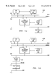
- FIGS. 1A and 1B are block diagrams respectively depicting two basic system architectures typical of those found in personal computers
- FIG. 2 illustrates a high level functional block diagram of a memory embodying the principles of the present invention
- FIG. 3 is a diagram of a highly enlarged small portion of the memory array shown in FIG. 2;
- FIG. 4 is a diagram of a highly enlarged memory cell of FIG. 3.
- FIG. 5 is a timing diagram illustrating a typical operation of the memory of FIG. 2;
- FIG. 6 is an elevational drawing of a semiconductor device embodying the principles of the present invention.
- FIGS. 7A and 7B are a functional block diagram and a package pinout for a second memory embodying the principles of the present invention.
- FIG. 8 is a timing diagram illustrating a typical operation of the memory of FIG. 7;
- FIG. 9A is a high level functional block diagram of a memory according to the present concepts utilizing blocks of memory circuitry organized into an array
- FIG. 9B is a more detailed functional block diagram of a selected one of the blocks of memory circuitry shown in FIG. 9A;
- FIG. 10A is a timing diagram depicting the operation of a synchronous dynamic random access memory with a nonmultiplexed address port
- FIG. 10B is a timing diagram depicting the operation of a synchronous dynamic random access memory with a nonmultiplexed address port embodying the principles of the present invention
- FIG. 10C is a timing diagram depicting the operation of a synchronous dynamic random access memory with a multiplexed address port.
- FIG. 10D is a timing diagram depicting the operation of a synchronous dynamic random access memory with a multiplexed address port embodying the principles of the present invention.
- FIGS. 1-5 of the drawings in which like numbers designate like parts.
- FIGS. 1A and 1B are block diagrams respectively depicting two basic system architectures 100 A and 100 B typical of those found in personal computers (PCS). While numerous variations on these basic architectures exist, FIGS. 1A and 1B are suitable for describing the basic structure and operation of most PCS.
- Both systems 100 A and 100 B include a single central processing unit 101 , CPU local data bus 102 , CPU local address bus 103 , external (L 2 ) cache 104 , core logic/memory controller 105 , and system memory 106 .
- the peripherals 108 are coupled directly to core logic/memory controller 105 via a bus 107 .
- Bus 107 in this case is preferably a peripheral controller interface (PCI) bus, although alternatively it could be an ISA, general, or special purpose bus, as known in the art.
- PCI peripheral controller interface
- core logic/memory controller 105 is again coupled to bus 107 .
- a PCI bus bridge then interfaces bus 107 with a PCI bus 110 , to which the peripherals 111 couple.
- An additional bus 112 which may be an ISA, PCI, VESA, IDE, general, or special purpose bus, is provided for access to peripherals 111 from an external device or system (not shown).
- CPU 101 In single CPU systems 100 A and 100 B, CPU 101 is the “master” which, in combination with the operating system and applications software, controls the overall operation of system 100 . Among other things, CPU 101 performs various data processing functions including numerical and word processing, generates graphics data, and performs overall system management.
- CPU 101 may be for example a complex instruction set computer (CISC), such as an Intel PentiumTM class microprocessor, a reduced instruction set computer (RISC), such as an Apple PowerPCTM microprocessor, or a very long instruction word (VLIW) machine.
- CISC complex instruction set computer
- RISC reduced instruction set computer
- VLIW very long instruction word
- CPU 101 communicates with the remainder of system 100 via CPU local data and address buses 102 and 103 , each of which may be for example a special bus, or a general bus, as known in the art.
- Core logic/memory controller 105 under the direction of CPU 101 , controls the exchange of data, addresses, control signals and instructions between CPU 101 , system memory 105 , and peripherals 108 / 111 via bus 107 and/or PCI bus bridge 109 .
- the core logic/memory controller allows tasks to be shifted from the CPU, thereby allowing the CPU to attend to other CPU-intensive tasks, the CPU can always override core logic/memory controller 105 to initiate execution of a higher priority task.
- the memory controller can be either a separate device or incorporated into the same chip set as the core logic.
- the memory controller is generally responsible for generating the memory clocks and control signals such as SCLK (System Clock) /RAS, /CAS, R/W and bank select, and monitors and controls cell refresh.
- SCLK System Clock
- R/W Random Access Memory
- the memory controller may also have some address generation capability for accessing sequences of pages.
- the core logic is typically comprised of a chip-set, with one or more chips typically being “address and system controller intensive” and one or more chips typically being “data intensive.”
- the address intensive chip(s) interfaces CPU 101 with address bus 103 ; maintains cache coherency, including the cache tags, set associative cache tags and other data necessary to insure cache coherency; performs cache “bus snooping”; generates the control signals required for DRAMs in the system memory or cache; and controls general management transactions.
- the data intensive chip(s) generally: interfaces CPU 101 with the data bus 102 ; issues cycle completion responses; may abort operations if their cycles are incomplete; and arbitrates for the data path of bus 102 .
- L 2 cache 104 may be for example a 256 KByte fast SRAM device(s). Typically, the CPU also maintains up to 16 kilobytes of on-chip (L 1 ) cache.
- PCI bus bridges such as PCI bus bridge 109
- PCI bus bridge 109 are also well known to those skilled in the art.
- the CPU is the bus master for the entire system and hence devices such as PCI bus bridge are slave devices which operate under command of the CPU.
- Peripherals 108 / 111 may include a display controller and associated frame buffer, floppy drive controller, disk driver controller, and/or modem, to name only a few options.
- FIG. 2 is a high level functional block diagram of a DRAM memory 200 embodying the teachings of the present invention.
- Memory 200 is suitable for such applications as system memory 106 in either of the exemplary processing environments shown in FIGS. 1A and 1B. Many other applications of memory 200 are possible.
- Memory 200 includes an array 201 organized as a pair of subarrays 201 a and 201 b (collectively array 201 ), each composed of rows and columns of DRAM cells. Each row of cells is associated with at least two conductive wordlines and each column of cells is associated with at least two conductive bitlines. This unique double bitline/double wordline approach will be discussed in detail below.
- a row of cells in array 201 is selected in response to a received row address by one of the row decoders 202 a or 202 b.
- the given decoder activates one of the pair of conductive wordlines associated with that row.
- Data is input to or output from, each selected cell along the row through one of the pair of bitlines associated with the corresponding column and the column decoder 204 in response to a received column address.
- sense amplifiers 203 During a read, the data from the entire active row of cells are sensed and latched by sense amplifiers 203 . For discussion purposes, it will be assumed that the bitlines are coupled to sense amplifiers 203 and read buffers (block 207 ). During a write, data are transferred to the locations addressed by the column address along the active row by the write buffers (block 207 ) directly through sense amps 203 (the data in sense amplifiers 203 are essentially written over).
- the data passed by sense amps 203 are selectively input to or output from device 200 through Z+1 number of access data input/output lines (DQ[ 0 :Z]) in response to row and column addresses received at Y+1 number of corresponding multiplexed access address lines (ADD[ 0 :Y]).
- DQ[ 0 :Z] access data input/output lines
- ADD[ 0 :Y] corresponding multiplexed access address lines
- Row addresses are latched into address latches within block 207 through the multiplexed address lines on the falling edge of external /RAS. At least one column address is similarly latched through the access address lines on the falling edge of external /CAS. (For page and burst mode accesses, column addresses can be generated externally and input with external /CAS or can be generated internally). External /RAS is also used to time the precharging of only one of the two bitlines associated with each column of cells (as discussed below, the other bitline in each column is used for refresh and has a precharge timing based on an internal /RAS signal or clock).
- Block 207 generally includes the traditional input/output circuitry, including read and write buffers, address latches, power distribution circuitry and clock generation circuitry. If DRAM 200 is a synchronous DRAM, it will include the synchronous DRAM master clock (CLK) which controls the overall timing.
- CLK synchronous DRAM master clock
- DRAM 200 further includes internally a refresh/precharge controller 208 , precharge circuitry 209 and multiplexers 210 .
- this circuitry allows for the data in selected rows of cells in the array to be refreshed simultaneously with data accesses to other selected rows in the array. Since entire rows are read and restored during refresh (i.e. there is no paging or bursting during refresh) the internal refresh /RAS active period controlling precharge circuitry 208 / 209 during refresh operations can be relatively short. In other words, the internal /RAS controlling precharge of the refresh bitlines can run not only asynchronously with respect to the external /RAS, but also at a much higher frequency.
- FIG. 3 depicts a portion of subarrays 201 a and 201 b and the corresponding sense amplifiers 203 .
- FIG. 3 shows three exemplary physical columns (Columns 0 , 1 and n) and two exemplary rows (Rows 0 and 1 ) of an m row by n column array, with respective halves of the rows disposed in one of the subarrays 201 a or 201 b.
- each cell 301 in each subarray 201 is coupled to a pair of bitlines 302 a and 302 b (labeled BL i A and BL i B, where i is the column number between 0 and n) and a pair of wordlines 303 a and 303 b (labeled WL j A and WL j B, where j is the row number between 0 and m).
- Each bitline 302 a/ 302 b of each column is coupled to a corresponding dedicated sense amplifier 304 a or 304 b, with the corresponding bitlines of subarrays 201 a and 201 b coupled to the same sense amplifier 304 being complementary.
- the even numbered pairs of wordlines 303 i.e. 0, 2, 4 . . .
- the odd numbered pairs i.e., 1, 3, 5 . . .
- Cells 301 are preferably constructed as the 2-transistor, 1-capacitor (2T-1C) cell depicted in FIG. 4 .
- 2T-1C 2-transistor, 1-capacitor
- Each cell includes a first pass transistor 401 a for coupling a first plate of data storage capacitor 402 with bitline BL 0 A in response to an active (high) voltage impressed on WL 0 A.
- a second pass transistor 401 b similarly selectively couples the storage capacitor 402 to bitline BL 0 B when an active (high) voltage is presented on wordline WL 0 B.
- selected rows in array 201 can be accessed while other selected rows are simultaneously refreshed.
- simultaneous access and refresh operations can be accomplished by using one bitline of each column and one wordline of each row for data accesses through access port 205 and the other bitline of each column and the other wordline of each row for refresh under control of internal refresh/precharge controller 208 .
- addresses internally generated for refresh by refresh controller 208 are decoded to exclusively access wordlines WL j A, with refresh effectuated by bitlines BL i A and the corresponding sense amplifiers 304 a. Consequently, addresses received at access port 205 are decoded to exclusively access wordlines and bitlines WL j B and BL i B through sense amplifiers 304 b.
- FIG. 5 is a simplified conceptual timing diagram. It should be noted that while a traditional operating scheme using /RAS and /CAS is shown, these strobes are not required in every embodiment of the present teachings. For example, in synchronous embodiments, all timing can be based solely on the system clock (CLK.)
- a row address is latched in to select the wordline WL j B associated with the row to which the desired data access is being performed.
- the selected row can be any row in array 201 ; however, for discussion purposes assume that the Row 1 has been selected for access. Shortly after the external /RAS transitions low, the voltage on wordline WL j B transitions high, the pass transistor 401 b of each cell 301 of Row 1 turns-on and the capacitors 402 of that row are available for access through bitlines BL i B.
- bitlines BL i B of subarray 201 a carry data to sense amplifiers 304 b and bitlines BL i B of subarray 201 b are used as the complementary bitlines for sensing purposes.
- the data in sense amplifiers 304 b are overwritten as new data is driven from the write buffers within block 207 .
- a column address is latched-in through the address lines of access port 205 and words of data are transferred to or from the sense amplifiers 304 b of the addressed columns via the data lines of access port 205 (/CAS can also be generated internally on-chip).
- the width of each word of data is a design choice; for example, in a “by 16” device 16 bits are accessed per column address (/CAS cycle).
- the number of words paged in or out with each new column address during the time when /RAS is low can vary from one up to the maximum number of words per row, depending on the application.
- refresh is performed by refresh/precharge controller 208 independent of any data accesses made through access port 205 .
- an internal /RAS signal or similar clock controls the refresh timing asynchronous to the externally generated signals controlling the data accesses (e.g. external /RAS and /CAS).
- the refresh operations are being timed by an internal /RAS signal, although these operations can also be timed off an internal clock generated by the system clock.
- refresh/precharge controller 208 and precharge circuitry 209 precharge bitlines BL i A of array 201 . Then, on the falling edge of internal /RAS, the active refresh period begins.
- Refresh/ precharge controller 208 generates a refresh row address to any row in array 201 . Specifically, this refresh row address selects the wordline WL j A of the row to be refreshed; assume for example wordline WL 0 A of Row 0 . The row address is decoded, wordline WL 0 A is activated and pass transistors 401 a of each of the cells along Row 0 turn-on.
- Row 0 The data stored in Row 0 are then read and restored by sense amplifiers 304 a through bitlines BL i A. On the rising edge of /RAS, bitlines BL i A are then returned to precharge. These row refresh cycles can be continuously performed essentially independently from the data access being performed through the access port and the external /RAS timing.
- Controller 208 can refresh bitlines using any one of a number of schemes. For example, it can simply sequentially generate row addresses using a counter and refresh the rows in the entire array 201 in sequence beginning from Row 0 . Alternatively, refresh can be done on a subarray by subarray basis, a distributed block by block basis, or even a distributed row by row basis.
- the primary advantage of the present teachings is that since one or more rows can be refreshed while another row is accessed, embodying devices can operate significantly faster.
- the refresh rate can be significantly increased over conventional DRAM devices. Increased refresh rate in turn allows for a higher tolerable leakage rate for the capacitors in the cells in the DRAM cell array.
- the higher dielectric constant materials necessary to make smaller planar storage capacitors 402 can be used, and hence smaller cells 301 , can be fabricated without the need for stacked or trench capacitor technologies.
- higher cell leakage is tolerable, the triple-well process and the accompanying charge pumps can be eliminated.
- An exemplary cell according to the present teachings may for example have the following leakage characteristics, defined in terms of tREF, which is the refresh time between tREF max and tREF min :
- tREF max 3.8 microseconds ⁇ number of rows in array 201 ;
- tREF min tRESTORE ⁇ number of rows in array 201 .
- tREF max is the maximum time between refresh cycles for a given row of cells
- tREF min is the minimum time between refresh cycles for a given row of cells.
- tRESTORE is the time from a row address change until the sense/restore function of the addressed row is complete in the minimum amount of time achievable in the fabrication and design technology applied.
- FIG. 6 is a highly enlarged portion of a semiconductor chip 600 embodying the circuitry of the present invention.
- both array 201 and peripheral circuitry 601 can now be formed in the same substrate 602 (without the need for the isolated p-well for array 201 ).
- all n-channel transistors in periperhy 601 and array 201 are now formed in a p-substrate 602 .
- FIG. 7A is a functional block diagram of a second memory 700 embodying the principles of the present invention.
- Memory 700 is a dynamic memory which does not require /RAS and /CAS and consequently emulates a static random access memory (SRAM).
- SRAM static random access memory
- such an embodiment does not require refresh control demands be imposed on the system, as well as no requirement for RAS, CAS, or a multiplexed addressing scheme.
- memory 700 emulates an SRAM memory module to the ASIC designer.
- Memory 700 eliminates bus contention problems during refresh, as seen in conventional DRAM designs. Further, the need for a conventional DRAM memory controller within the core logic is eliminated.
- memory 700 is based on a 2 megabyte (2097152 ⁇ 8 bit) array 701 of memory cells 301 , although the size of array will vary depending on the application and/or the process used in its fabrication. For purposes of discussion, assume that array 701 is partitioned into 256 subarrays organized as a 16 ⁇ 16 matrix, with the memory cells in each subarray arranged in 256 rows and 256 columns. A preferred subarray structure will be discussed in conjunction with FIGS. 9A and 9B.
- Memory 700 essentially consists of two sets of addressing and control circuitry.
- the first set is used to enable data accesses to locations in array 701 and generally includes: an access row decoder 702 , access sense amplifiers 703 , access column decoder 704 , access read-write amplifiers 705 , buffers 706 a and 706 b, control gates 707 a and 707 b, access sense amplifier controls 708 , and new address detection circuitry 709 .
- the second set of addressing and control circuitry is dedicated to array refresh and includes refresh sense amplifiers 710 , refresh row decoder 711 , refresh row address generator 712 , sense amplifier control circuitry 713 and comparator 714 .
- Memory 700 also includes an on-chip clock generator 715 . Each of these blocks and the interactions there between can now be discussed in detail.
- Access row decoder 702 receives 12 row address bits A[ 11 : 0 ] and in response selects a wordline WL j B in array 701 .
- the 12 row address bits are received by memory 700 simultaneously with the receipt of 9 column address bits A[ 20 : 12 ] in a single 21 bit address word A[ 20 : 0 ]from a non-multiplexed address bus.
- Access row decoder 702 is enabled each time a new set of address bits are detected by new address detection circuitry 709 .
- the row and column address bits may be received word-serial from a multiplexed address bus, timed by an external clock or control signal.
- Access sense amplifiers are shown generally at 703 , preferably they are distributed across array 701 , for example on a subarray by subarray basis (Distributed sense amplifiers will be discussed further in conjunction with FIGS. 9 a and 9 b ).
- each bitline BL i B and its complement /BL i B are coupled to a sense amplifier 304 in an open bitline fashion as shown in FIG. 3 although a folded bitline could also be used.
- Access sense amplifiers 703 are dedicated to precharging and equalizing bitlines BL i B of a corresponding subarray during each bitline precharge cycle and to latching data for presentation to the read and write amplifiers 705 during each bitlines access cycle, as discussed above. Control of access sense amplifiers 703 is effectuated by access sense amplifier control unit 708 and column decoder 704 .
- Access column decoder 704 receives the nine column address bits (A[ 20 : 12 ]) of each address word A[ 20 : 0 ] and decodes these bits into a set of signals driving a set of Y-lines. These Y-lines in turn are connected to data transfer transistors in access sense amplifiers 703 which gate data exchanges between locations (a cell or group of cells) in the corresponding subarray and the read-write amplifiers 705 . Reads and writes through read-write amplifiers 705 and I/O buffers 706 are controlled by the externally generated output enable (/OE), chip enable (/CE) and write enable (/WE) signals.
- /OE output enable
- CE chip enable
- /WE write enable
- Access sense amplifier control circuitry 708 enables and times such sense amplifier functions as bitline equalization, bitline isolation, and sense and restore, under the control of new address detection circuitry 709 .
- this circuitry allows the access bitlines BL i B to be precharged and accessed independently from the refresh precharge and sense and restore operations.
- new address detection circuitry 709 detects when a change in the row address bits has occurred. When a change in row address occurs, and memory 700 is currently in an access cycle (e.g., words are being paged to or from the current row through a sequence of column addresses), that cycle is allowed to complete and then a new access cycle to a new row is initiated.
- the output of new address detection circuitry 709 is used to enable the functioning of access row address decoders 702 , column decoder 704 , and access sense amplifier control circuitry 708 .
- Refresh sense amplifiers 710 are coupled to bitlines BL i A and are dedicated to sensing and restoring the data in a row of cells along wordline (subwordline) WL j A in the corresponding subarray, in response to refresh addresses decoded by refresh row decoder 711 . As with the access sense amplifiers, refresh sense amplifiers 710 are preferably distributed across array 701 .
- Refresh row addresses are internally generated by row address generator 712 and provided to refresh decoder 711 for refresh row selection.
- Refresh address generator 712 in this example is a 12-bit counter which runs continuously from a minimum value to a maximum value, and then rolls-over to the minimum value again although other counting patterns are possible.
- Comparator 714 compares each refresh address output from address generator 712 with the current access row address. If the two are different, then the address from refresh generator 712 is used to refresh the addressed row in the corresponding subarray. When the refresh address and the access address match, refresh of the addressed row is foregone in favor of the access to that row. Assuming the maximum allowable time between refreshes for the foregone row of cells will not be exceeded, the cells of that row can be refreshed when the address generator reaches the corresponding address again. Alternatively, a timeout can be taken from the refresh sequence until the access is completed.
- Control of refresh sense amplifiers 710 is effectuated by refresh sense amplifier control circuitry 713 .
- control circuitry 713 times the bitline equalization, bitline isolation and sense and restore operations for refresh bitlines BL i A.
- FIG. 7B is an exemplary package/ pinout diagram supporting the 2 Mbyte embodiment of memory 700 described above.
- the packaging/pinout for memory 700 will vary from application to application, depending on such factors as the size of the array, the width of the address port and the width of the I/O port.
- memory 700 is operating synchronously in response to a system clock signal CLK.
- Clock signal CLK could be generated for example by the core logic/memory controller or by the CPU itself.
- CLK could be generated for example by the core logic/memory controller or by the CPU itself.
- An access cycle begins with the receipt of an address word selecting a given location along a given access wordline WL j B and a set of access bitlines BL i B.
- the first row access is depicted as a read operation, therefore the output enable signal /OE transitions to an active low state and the write enable signal /WE to an inactive high state.
- Word 0 is read from the addressed location through amplifiers 705 and buffers 706 a.
- additional column addresses generated internally or externally, are used to sequentially read a predetermined number of additional locations along wordline WL i B using additional access bitline BL i B (e.g., BL i+1 B, BL i+2 B, . . . ).
- refresh address generator 712 While data are being read through the I/O port (I/O [ 7 : 0 ]), refresh address generator 712 is generating a sequence of refresh addresses, refresh sense amplifier control circuitry 713 is initiating precharge, and active refresh cycles and rows of cells are being refreshed using refresh wordlines WL j+x A and refresh wordlines BL j A. As long as wordline WL j A is not selected simultaneously with WL j B, for a given value of j, the output of comparator 714 is in an active low state and sequence of row refreshes continues uninterrupted. As described above, the row refresh operations can advantageously be performed at a rate higher than the access operations and thus smaller and/or leakier capacitors can be used in the fabrication of array 701 .
- access wordline WL k B is selected by the access address and data paging begins with the initial column address selecting bitlines BL m B.
- a write is assumed and therefore the write enable signal /WE transitions to an active low state and the output enable signal /OE transitions to an inactive high state.
- Data e.g., word 0 , word 1 , . . .
- I/O port I/O [ 7 : 0 ]
- the refresh of array 701 has been continuing using wordlines WL j A and bitlines BL i A.
- the refresh address and the access address both address the same row of cells in array 701 , albeit through different wordlines and bitlines (in the illustrate example, the refresh address selects wordline WL k A and the access address selects wordline WL k B).
- the output of the comparator transitions to an inactive high state and the refresh of the addressed row via wordline WL k A is foregone or postponed in lieu of the data access along wordline (row) WL k B.
- the comparator output transitions to active low again and the refresh resumes with either the new addressed refreshed row (if the current row was skipped) or the currently addressed refresh row (in the case where the refresh was simply delayed pending completion of the access to that row.)
- FIG. 9A depicts in detail the partitioning of array 701 into a predetermined number of blocks each including a subarray of cells and accompanying distributed access and refresh circuitry, collectively designated as a subarray 901 .
- the details of each block 901 are shown in FIG. 9 B.
- array 701 overall is a 16 megabit array which is divided into 64 subarrays organized in 8 rows and 8 columns.
- Each subarray 901 comprises a 256 kbit cell subarray 902 (FIG. 9B) organized as 1024 rows by 256 columns.
- the number of address bits consequently required to access each row of array 900 is thirteen (13).
- the number of column address bits required to access groups of eight (8) columns for a “by 8” embodiment is eight (8) bits.
- Two sets of access controls are provided in each block 901 , one set for location (data) accesses and one set for row refreshes.
- the access control circuitry includes access sense amplifiers (ASA) 903 and shunts (AS) 904 a and 904 b, each of which is coupled to and controlled by access sense amplifier control circuitry 708 .
- Access row selection is effectuated by access subwordline driver (ASD) 905 in response to the selection of a wordline WL j B and a signal presented on access X-decode line XA q .
- ASD access subwordline driver
- the refresh control circuitry includes refresh sense amplifiers (RSA) 906 and refresh shunts (RS) 907 a and 907 b, each of which is coupled to and controlled by refresh sense amplifier control circuitry 713 .
- Row selection is effectuated by refresh subwordline driver (RSD) 908 in response to the selection of a wordline WL j A and refresh a X-decode line XRq.
- RSD refresh subwordline driver
- FIGS. 9A and 9B also advantageously allows for the performance of operations during which only the bitlines of a single block or row of blocks of 901 being accessed and/or refreshed are precharged and equalized.
- bitlines BL i A and BL i B of a single row of blocks can be precharged/equalized and both accesses and row refreshes concurrently performed as discussed above, or the bitlines BL i A of one row of blocks precharged for refreshes and the bitlines BL i B of a second row of blocks 901 precharged and used for accesses.
- many combinations of accesses and refresh operations are possible since the memory is partitioned into independent subarrays.
- the present concepts also allow for low-latency operation of DRAMs with either multiplexed or non-multiplexed address ports. These operations are illustrated in the timing diagrams of FIGS. 10A-10D, with FIGS. 10A and 10B comparing the operation of a conventional SDRAM with a non-multiplexed address port and that of a memory embodying the inventive concepts.
- FIGS. 10C and 10D an SDRAM is again compared against a memory according to the invention, except in this case, a multiplexed address port is considered.
- 2T-1C memories 400 and 700 will be assumed as the memory configurations, although the described low-latency concepts can be applied to other memory configurations and architectures.
- the timing relationships e.g. number of clock periods between address inputs, the number of clock periods representing the random cycle time
- rising edges have been chosen for reference, although timing off falling edges or voltage levels are also acceptable.
- FIG. 10A shows the operation of an SDRAM with a nonmultiplexed address port CMD.
- an address to the device can be input on every fourth rising clock edge, with valid data available in response to each address after a delay of three clocks thereafter. Data is effectively available to the system every fourth clock period. Therefore, for a 100 MHZ clock, the fastest rate that data is available is roughly every 40 nanoseconds.
- the non-multiplexed embodiment of the present concepts provides data at essentially twice the rate of a conventional SDRAM, as shown in FIG. 10 B. Unlike the SDRAM discussed above, addresses are input on every other, instead of every fourth clock edge. As a result, after the first random cycle, data is available every other clock edge.
- Addressing a memory, for instance memory 700 is achieved by interleaving accesses between bitline sets BLA and BLB using wordlines WLA and WLB, respectively.
- the first address depicted is used to access a location using selected bitlines BL i A along a wordline WL j A.
- bitlines BL i A return to precharge.
- an address is input for accessing a storage location using the bitlines BL i B and a wordline WL j A.
- the data is available in response to the first address. This process continues as long as required. For a 100 MHZ clock, valid data is available every 20 nanoseconds.
- a similar increase in data rate is also realized in the multiplexed address port embodiment.
- typical random access works as follows. A row address, input on a corresponding rising edge of the clock. After at least two rising edges later, the column address is clocked into the device. Valid data is finally available on the next rising edge of the clock. Again, the random cycle time is four clock periods. For a 100 MHZ clock after the first random access, random data is available only every 40 nanoseconds.
- random data is available at twice the rate as a consequence of interleaving accesses between the two sets of bitlines BLA and BLB.
- an address to Row A is input to a first port to select a wordline WL j A.
- a column address is input for accessing cells along wordline WL j A using bitlines BL i A.
- a row address is input to a second port for accessing Row B using a corresponding bitline BL i B.
- Valid data is available from the addressed cells in Row A on the next rising clock edge.
- the column address to Row B is input to the second port along with a new row address on the first port to select a row (Row C) using the corresponding wordline WL k A.
- the data from Row B is accessed, and the cycle continues with the input on the first port of the column address to Row C (bitlines BL i A) This process continues, with random data available at twice the rate of a conventional SDRAM.
Abstract
Description
Claims (25)
Priority Applications (1)
| Application Number | Priority Date | Filing Date | Title |
|---|---|---|---|
| US09/295,641 US6233193B1 (en) | 1998-05-18 | 1999-04-20 | Dynamic random access memory system with a static random access memory interface and methods for using the same |
Applications Claiming Priority (2)
| Application Number | Priority Date | Filing Date | Title |
|---|---|---|---|
| US09/080,813 US5963497A (en) | 1998-05-18 | 1998-05-18 | Dynamic random access memory system with simultaneous access and refresh operations and methods for using the same |
| US09/295,641 US6233193B1 (en) | 1998-05-18 | 1999-04-20 | Dynamic random access memory system with a static random access memory interface and methods for using the same |
Related Parent Applications (1)
| Application Number | Title | Priority Date | Filing Date |
|---|---|---|---|
| US09/080,813 Continuation-In-Part US5963497A (en) | 1998-05-18 | 1998-05-18 | Dynamic random access memory system with simultaneous access and refresh operations and methods for using the same |
Publications (1)
| Publication Number | Publication Date |
|---|---|
| US6233193B1 true US6233193B1 (en) | 2001-05-15 |
Family
ID=22159783
Family Applications (2)
| Application Number | Title | Priority Date | Filing Date |
|---|---|---|---|
| US09/080,813 Expired - Lifetime US5963497A (en) | 1998-05-18 | 1998-05-18 | Dynamic random access memory system with simultaneous access and refresh operations and methods for using the same |
| US09/295,641 Expired - Lifetime US6233193B1 (en) | 1998-05-18 | 1999-04-20 | Dynamic random access memory system with a static random access memory interface and methods for using the same |
Family Applications Before (1)
| Application Number | Title | Priority Date | Filing Date |
|---|---|---|---|
| US09/080,813 Expired - Lifetime US5963497A (en) | 1998-05-18 | 1998-05-18 | Dynamic random access memory system with simultaneous access and refresh operations and methods for using the same |
Country Status (5)
| Country | Link |
|---|---|
| US (2) | US5963497A (en) |
| EP (1) | EP1004119A4 (en) |
| JP (1) | JP2002516452A (en) |
| KR (1) | KR20010021966A (en) |
| WO (1) | WO1999060573A1 (en) |
Cited By (18)
| Publication number | Priority date | Publication date | Assignee | Title |
|---|---|---|---|---|
| US6388934B1 (en) * | 2000-10-04 | 2002-05-14 | Mitsubishi Denki Kabushiki Kaisha | Semiconductor memory device operating at high speed with low current consumption |
| US6438016B1 (en) | 2000-08-30 | 2002-08-20 | Micron Technology, Inc. | Semiconductor memory having dual port cell supporting hidden refresh |
| US6452834B1 (en) * | 2001-02-13 | 2002-09-17 | Silicon Access Networks | 2T dual-port DRAM in a pure logic process with non-destructive read capability |
| US6553328B1 (en) * | 2000-02-18 | 2003-04-22 | Hughes Electronics Corp. | Non-intrusive memory access for embedded processors |
| US6600677B2 (en) * | 2000-05-16 | 2003-07-29 | Broadcom Corporation | Memory circuit capable of simultaneous writing and refreshing on the same column and a memory cell for application in the same |
| US6621752B2 (en) * | 2001-10-03 | 2003-09-16 | Infineon Technologies Aktiengesellschaft | Refreshing scheme for memory cells a memory array to increase performance of integrated circuits |
| US20040042311A1 (en) * | 2002-08-28 | 2004-03-04 | Fujitsu Limited | Semiconductor memory |
| US6711081B1 (en) * | 2002-09-19 | 2004-03-23 | Infineon Technologies Aktiengesellschaft | Refreshing of multi-port memory in integrated circuits |
| US6721840B1 (en) * | 2000-08-18 | 2004-04-13 | Triscend Corporation | Method and system for interfacing an integrated circuit to synchronous dynamic memory and static memory |
| US20040081006A1 (en) * | 2002-10-23 | 2004-04-29 | Nec Electronics Corporation | Semiconductor memory device and control method thereof |
| US6757209B2 (en) * | 2001-03-30 | 2004-06-29 | Intel Corporation | Memory cell structural test |
| US20050162960A1 (en) * | 2004-01-28 | 2005-07-28 | Nec Electronics Corporation | Semiconductor integrated circuit device |
| US6958944B1 (en) * | 2004-05-26 | 2005-10-25 | Taiwan Semiconductor Manufacturing Co., Ltd. | Enhanced refresh circuit and method for reduction of DRAM refresh cycles |
| US20060004955A1 (en) * | 2002-06-20 | 2006-01-05 | Rambus Inc. | Dynamic memory supporting simultaneous refresh and data-access transactions |
| US20060239092A1 (en) * | 2005-04-26 | 2006-10-26 | Chi-Ting Cheng | Memory Circuit And Related Method For Integrating Pre-Decoding And Selective Pre-Charging |
| US20110141836A1 (en) * | 2009-12-16 | 2011-06-16 | Innovative Silicon Isi Sa | Techniques for reducing impact of array disturbs in a semiconductor memory device |
| CN104795109A (en) * | 2014-01-22 | 2015-07-22 | 南亚科技股份有限公司 | Dynamic random access memory and method of selectively performing refresh operation |
| US11195568B1 (en) * | 2020-08-12 | 2021-12-07 | Samsung Electronics Co., Ltd. | Methods and systems for controlling refresh operations of a memory device |
Families Citing this family (27)
| Publication number | Priority date | Publication date | Assignee | Title |
|---|---|---|---|---|
| US6181619B1 (en) * | 1998-12-04 | 2001-01-30 | Intel Corporation | Selective automatic precharge of dynamic random access memory banks |
| JP4050839B2 (en) | 1999-01-29 | 2008-02-20 | 松下電器産業株式会社 | Semiconductor memory device |
| JP3618241B2 (en) * | 1999-02-02 | 2005-02-09 | 松下電器産業株式会社 | Semiconductor memory device |
| US6094397A (en) * | 1999-02-09 | 2000-07-25 | International Business Machines Corporation | Method and apparatus for addressing multi-bank memory |
| US6646941B1 (en) * | 1999-04-30 | 2003-11-11 | Madrone Solutions, Inc. | Apparatus for operating an integrated circuit having a sleep mode |
| JP4555416B2 (en) * | 1999-09-22 | 2010-09-29 | 富士通セミコンダクター株式会社 | Semiconductor integrated circuit and control method thereof |
| US6259634B1 (en) * | 2000-05-22 | 2001-07-10 | Silicon Access Networks, Inc. | Pseudo dual-port DRAM for simultaneous read/write access |
| JP3708801B2 (en) * | 2000-06-16 | 2005-10-19 | 松下電器産業株式会社 | Semiconductor memory device |
| US6697909B1 (en) * | 2000-09-12 | 2004-02-24 | International Business Machines Corporation | Method and apparatus for performing data access and refresh operations in different sub-arrays of a DRAM cache memory |
| US7085186B2 (en) * | 2001-04-05 | 2006-08-01 | Purple Mountain Server Llc | Method for hiding a refresh in a pseudo-static memory |
| KR100401506B1 (en) * | 2001-05-10 | 2003-10-17 | 주식회사 하이닉스반도체 | Synchronous memory device having asynchronous precharge |
| US6400629B1 (en) | 2001-06-29 | 2002-06-04 | International Business Machines Corporation | System and method for early write to memory by holding bitline at fixed potential |
| US6504766B1 (en) | 2001-06-29 | 2003-01-07 | International Business Machines Corporation | System and method for early write to memory by injecting small voltage signal |
| US6738887B2 (en) | 2001-07-17 | 2004-05-18 | International Business Machines Corporation | Method and system for concurrent updating of a microcontroller's program memory |
| JP4768163B2 (en) * | 2001-08-03 | 2011-09-07 | 富士通セミコンダクター株式会社 | Semiconductor memory |
| JP2004094338A (en) * | 2002-08-29 | 2004-03-25 | Seiko Epson Corp | Semiconductor integrated circuit |
| JP2005216340A (en) * | 2004-01-28 | 2005-08-11 | Nec Electronics Corp | Semiconductor memory device |
| US7208398B2 (en) * | 2004-03-17 | 2007-04-24 | Texas Instruments Incorporated | Metal-halogen physical vapor deposition for semiconductor device defect reduction |
| US20050289293A1 (en) * | 2004-06-28 | 2005-12-29 | Parris Michael C | Dual-port DRAM cell with simultaneous access |
| US7154795B2 (en) * | 2004-07-30 | 2006-12-26 | United Memories, Inc. | Clock signal initiated precharge technique for active memory subarrays in dynamic random access memory (DRAM) devices and other integrated circuit devices incorporating embedded DRAM |
| US7957212B2 (en) * | 2005-03-31 | 2011-06-07 | Hynix Semiconductor Inc. | Pseudo SRAM |
| KR100838390B1 (en) * | 2005-03-31 | 2008-06-13 | 주식회사 하이닉스반도체 | Pseudo sram |
| US7145829B1 (en) | 2005-06-16 | 2006-12-05 | International Business Machines Corporation | Single cycle refresh of multi-port dynamic random access memory (DRAM) |
| US7330391B2 (en) * | 2005-10-17 | 2008-02-12 | Infineon Technologies Ag | Memory having directed auto-refresh |
| WO2012074724A1 (en) * | 2010-12-03 | 2012-06-07 | Rambus Inc. | Memory refresh method and devices |
| CN107180649B (en) * | 2016-03-11 | 2021-01-15 | 联华电子股份有限公司 | Semiconductor memory device and method of operating semiconductor memory device |
| US10074422B1 (en) * | 2017-06-13 | 2018-09-11 | Cypress Semiconductor Corporation | 2T1C ferro-electric random access memory cell |
Citations (4)
| Publication number | Priority date | Publication date | Assignee | Title |
|---|---|---|---|---|
| US4203159A (en) * | 1978-10-05 | 1980-05-13 | Wanlass Frank M | Pseudostatic electronic memory |
| US5007022A (en) * | 1987-12-21 | 1991-04-09 | Texas Instruments Incorporated | Two-port two-transistor DRAM |
| US5010519A (en) * | 1987-11-17 | 1991-04-23 | Mitsubishi Denki Kabushiki Kaisha | Dynamic semiconductor memory device formed by 2-transistor cells |
| US5377142A (en) * | 1992-08-12 | 1994-12-27 | Mitsubishi Denki Kabushiki Kaisha | Semiconductor memory having data preset function |
Family Cites Families (2)
| Publication number | Priority date | Publication date | Assignee | Title |
|---|---|---|---|---|
| US5381379A (en) * | 1992-12-03 | 1995-01-10 | Sharp Kabushiki Kaisha | Non-volatile dynamic random access memory device; a page store device and a page recall device used in the same; and a page store method and a page recall method |
| US5636174A (en) * | 1996-01-11 | 1997-06-03 | Cirrus Logic, Inc. | Fast cycle time-low latency dynamic random access memories and systems and methods using the same |
-
1998
- 1998-05-18 US US09/080,813 patent/US5963497A/en not_active Expired - Lifetime
-
1999
- 1999-04-20 US US09/295,641 patent/US6233193B1/en not_active Expired - Lifetime
- 1999-05-17 JP JP2000550106A patent/JP2002516452A/en active Pending
- 1999-05-17 KR KR1020007000531A patent/KR20010021966A/en not_active Application Discontinuation
- 1999-05-17 EP EP99923158A patent/EP1004119A4/en not_active Withdrawn
- 1999-05-17 WO PCT/US1999/010892 patent/WO1999060573A1/en not_active Application Discontinuation
Patent Citations (4)
| Publication number | Priority date | Publication date | Assignee | Title |
|---|---|---|---|---|
| US4203159A (en) * | 1978-10-05 | 1980-05-13 | Wanlass Frank M | Pseudostatic electronic memory |
| US5010519A (en) * | 1987-11-17 | 1991-04-23 | Mitsubishi Denki Kabushiki Kaisha | Dynamic semiconductor memory device formed by 2-transistor cells |
| US5007022A (en) * | 1987-12-21 | 1991-04-09 | Texas Instruments Incorporated | Two-port two-transistor DRAM |
| US5377142A (en) * | 1992-08-12 | 1994-12-27 | Mitsubishi Denki Kabushiki Kaisha | Semiconductor memory having data preset function |
Non-Patent Citations (1)
| Title |
|---|
| "Transparent-Refresh DRAM (TreD) Using Dual-Port DRAM Cell" by Sakurai, Nogami, Sawada and Iizuka, 1988 IEEE Custom Integrated Circuits Conference p. 4.3.1 through4.3.4. |
Cited By (35)
| Publication number | Priority date | Publication date | Assignee | Title |
|---|---|---|---|---|
| US6553328B1 (en) * | 2000-02-18 | 2003-04-22 | Hughes Electronics Corp. | Non-intrusive memory access for embedded processors |
| US20030202384A1 (en) * | 2000-05-16 | 2003-10-30 | Broadcom Corporation | Transparent continuous refresh RAM cell architecture |
| US6600677B2 (en) * | 2000-05-16 | 2003-07-29 | Broadcom Corporation | Memory circuit capable of simultaneous writing and refreshing on the same column and a memory cell for application in the same |
| US6888761B2 (en) | 2000-05-16 | 2005-05-03 | Broadcom Corporation | Memory device having simultaneous read/write and refresh operations with coincident phases |
| US6717863B2 (en) | 2000-05-16 | 2004-04-06 | Broadcom Corporation | Transparent continuous refresh RAM cell architecture |
| US20040184335A1 (en) * | 2000-05-16 | 2004-09-23 | Broadcom Corporation | Transparent continuous refresh RAM cell architecture |
| US6721840B1 (en) * | 2000-08-18 | 2004-04-13 | Triscend Corporation | Method and system for interfacing an integrated circuit to synchronous dynamic memory and static memory |
| US6438016B1 (en) | 2000-08-30 | 2002-08-20 | Micron Technology, Inc. | Semiconductor memory having dual port cell supporting hidden refresh |
| US6757200B2 (en) | 2000-08-30 | 2004-06-29 | Micron Technology, Inc. | Semiconductor memory having dual port cell supporting hidden refresh |
| US6388934B1 (en) * | 2000-10-04 | 2002-05-14 | Mitsubishi Denki Kabushiki Kaisha | Semiconductor memory device operating at high speed with low current consumption |
| US6452834B1 (en) * | 2001-02-13 | 2002-09-17 | Silicon Access Networks | 2T dual-port DRAM in a pure logic process with non-destructive read capability |
| US6757209B2 (en) * | 2001-03-30 | 2004-06-29 | Intel Corporation | Memory cell structural test |
| US6621752B2 (en) * | 2001-10-03 | 2003-09-16 | Infineon Technologies Aktiengesellschaft | Refreshing scheme for memory cells a memory array to increase performance of integrated circuits |
| US7565480B2 (en) | 2002-06-20 | 2009-07-21 | Rambus Inc. | Dynamic memory supporting simultaneous refresh and data-access transactions |
| US20060004955A1 (en) * | 2002-06-20 | 2006-01-05 | Rambus Inc. | Dynamic memory supporting simultaneous refresh and data-access transactions |
| US10593390B2 (en) | 2002-06-20 | 2020-03-17 | Rambus Inc. | Dynamic memory supporting simultaneous refresh and data-access transactions |
| US9824740B2 (en) | 2002-06-20 | 2017-11-21 | Rambus Inc. | Dynamic memory supporting simultaneous refresh and data-access transactions |
| US20090248972A1 (en) * | 2002-06-20 | 2009-10-01 | Ware Frederick A | Dynamic Memory Supporting Simultaneous Refresh and Data-Access Transactions |
| US7043599B1 (en) * | 2002-06-20 | 2006-05-09 | Rambus Inc. | Dynamic memory supporting simultaneous refresh and data-access transactions |
| US20040042311A1 (en) * | 2002-08-28 | 2004-03-04 | Fujitsu Limited | Semiconductor memory |
| US6741516B2 (en) * | 2002-08-28 | 2004-05-25 | Fujitsu Limited | Semiconductor memory |
| US6711081B1 (en) * | 2002-09-19 | 2004-03-23 | Infineon Technologies Aktiengesellschaft | Refreshing of multi-port memory in integrated circuits |
| US20040081006A1 (en) * | 2002-10-23 | 2004-04-29 | Nec Electronics Corporation | Semiconductor memory device and control method thereof |
| US7002868B2 (en) * | 2002-10-23 | 2006-02-21 | Nec Electronics Corporation | High-speed, two-port dynamic random access memory (DRAM) with a late-write configuration |
| US7570535B2 (en) * | 2004-01-28 | 2009-08-04 | Nec Electronics Corporation | Semiconductor integrated circuit device having memory macros and logic cores on board |
| US20050162960A1 (en) * | 2004-01-28 | 2005-07-28 | Nec Electronics Corporation | Semiconductor integrated circuit device |
| US6958944B1 (en) * | 2004-05-26 | 2005-10-25 | Taiwan Semiconductor Manufacturing Co., Ltd. | Enhanced refresh circuit and method for reduction of DRAM refresh cycles |
| US7257041B2 (en) * | 2005-04-26 | 2007-08-14 | Via Technologies Inc. | Memory circuit and related method for integrating pre-decoding and selective pre-charging |
| US20060239092A1 (en) * | 2005-04-26 | 2006-10-26 | Chi-Ting Cheng | Memory Circuit And Related Method For Integrating Pre-Decoding And Selective Pre-Charging |
| US8310893B2 (en) * | 2009-12-16 | 2012-11-13 | Micron Technology, Inc. | Techniques for reducing impact of array disturbs in a semiconductor memory device |
| US20110141836A1 (en) * | 2009-12-16 | 2011-06-16 | Innovative Silicon Isi Sa | Techniques for reducing impact of array disturbs in a semiconductor memory device |
| CN104795109A (en) * | 2014-01-22 | 2015-07-22 | 南亚科技股份有限公司 | Dynamic random access memory and method of selectively performing refresh operation |
| US20150206575A1 (en) * | 2014-01-22 | 2015-07-23 | Nanya Technology Corp. | Counter based design for temperature controlled refresh |
| US9412433B2 (en) * | 2014-01-22 | 2016-08-09 | Nanya Technology Corp. | Counter based design for temperature controlled refresh |
| US11195568B1 (en) * | 2020-08-12 | 2021-12-07 | Samsung Electronics Co., Ltd. | Methods and systems for controlling refresh operations of a memory device |
Also Published As
| Publication number | Publication date |
|---|---|
| EP1004119A4 (en) | 2001-08-08 |
| EP1004119A1 (en) | 2000-05-31 |
| JP2002516452A (en) | 2002-06-04 |
| KR20010021966A (en) | 2001-03-15 |
| WO1999060573A1 (en) | 1999-11-25 |
| US5963497A (en) | 1999-10-05 |
Similar Documents
| Publication | Publication Date | Title |
|---|---|---|
| US6233193B1 (en) | Dynamic random access memory system with a static random access memory interface and methods for using the same | |
| US6418063B1 (en) | Memory architecture and systems and methods using the same | |
| US5856940A (en) | Low latency DRAM cell and method therefor | |
| US8503250B2 (en) | High speed DRAM architecture with uniform access latency | |
| KR950014905B1 (en) | A semiconductor memory device with an internal voltage generating circuit | |
| US6282606B1 (en) | Dynamic random access memories with hidden refresh and utilizing one-transistor, one-capacitor cells, systems and methods | |
| US7447098B2 (en) | Semiconductor memory device having complete hidden refresh function | |
| US20040174728A1 (en) | Semiconductor memory device | |
| US6751159B2 (en) | Memory device operable in either a high-power, full-page size mode or a low-power, reduced-page size mode | |
| US4079462A (en) | Refreshing apparatus for MOS dynamic RAMs | |
| US6510094B2 (en) | Method and apparatus for refreshing semiconductor memory | |
| US11114155B2 (en) | High-density high-bandwidth static random access memory (SRAM) with phase shifted sequential read | |
| US5982696A (en) | Memories with programmable address decoding and systems and methods using the same | |
| EP1421589B1 (en) | Multiple word-line accessing and accessor | |
| US7177216B2 (en) | Twin-cell bit line sensing configuration | |
| US5963468A (en) | Low latency memories and systems using the same | |
| US6594195B2 (en) | Low-power, high-density semiconductor memory device | |
| US10740188B2 (en) | Volatile memory device and method for efficient bulk data movement, backup operation in the volatile memory device | |
| KR100414716B1 (en) | SRAM compatible and Page Accessible Semiconductor Memory Device using DRAM cell Operating Method thereof | |
| US20240071469A1 (en) | Memory with single transistor sub-word line drivers, and associated systems, devices, and methods | |
| KR20030091431A (en) | asynchronous semiconductor memory device having minimizied radom access time and method therefore | |
| JPH09330595A (en) | Semiconductor memory and data processor |
Legal Events
| Date | Code | Title | Description |
|---|---|---|---|
| AS | Assignment |
Owner name: SILICON AQUARIUS, INC., TEXAS Free format text: ASSIGNMENT OF ASSIGNORS INTEREST;ASSIGNORS:HOLLAND, WAYLAND BART;SEITSINGER, STEPHEN;REEL/FRAME:009915/0976 Effective date: 19990417 |
|
| STCF | Information on status: patent grant |
Free format text: PATENTED CASE |
|
| FPAY | Fee payment |
Year of fee payment: 4 |
|
| AS | Assignment |
Owner name: S. AQUA SEMICONDUCTOR,DELAWARE Free format text: ASSIGNMENT OF ASSIGNORS INTEREST;ASSIGNOR:SILICON AQUARIUS, INCORPORATED;REEL/FRAME:019265/0434 Effective date: 20070423 Owner name: S. AQUA SEMICONDUCTOR, DELAWARE Free format text: ASSIGNMENT OF ASSIGNORS INTEREST;ASSIGNOR:SILICON AQUARIUS, INCORPORATED;REEL/FRAME:019265/0434 Effective date: 20070423 |
|
| AS | Assignment |
Owner name: S. AQUA SEMICONDUCTOR, LLC,DELAWARE Free format text: ASSIGNMENT OF ASSIGNORS INTEREST;ASSIGNOR:SILICON AQUARIUS, INCORPORATED;REEL/FRAME:019331/0414 Effective date: 20070423 Owner name: S. AQUA SEMICONDUCTOR, LLC, DELAWARE Free format text: ASSIGNMENT OF ASSIGNORS INTEREST;ASSIGNOR:SILICON AQUARIUS, INCORPORATED;REEL/FRAME:019331/0414 Effective date: 20070423 |
|
| FEPP | Fee payment procedure |
Free format text: PAT HOLDER NO LONGER CLAIMS SMALL ENTITY STATUS, ENTITY STATUS SET TO UNDISCOUNTED (ORIGINAL EVENT CODE: STOL); ENTITY STATUS OF PATENT OWNER: LARGE ENTITY |
|
| REFU | Refund |
Free format text: REFUND - PAYMENT OF MAINTENANCE FEE, 8TH YR, SMALL ENTITY (ORIGINAL EVENT CODE: R2552); ENTITY STATUS OF PATENT OWNER: LARGE ENTITY |
|
| FPAY | Fee payment |
Year of fee payment: 8 |
|
| SULP | Surcharge for late payment |
Year of fee payment: 7 |
|
| FPAY | Fee payment |
Year of fee payment: 12 |
|
| AS | Assignment |
Owner name: HANGER SOLUTIONS, LLC, GEORGIA Free format text: ASSIGNMENT OF ASSIGNORS INTEREST;ASSIGNOR:INTELLECTUAL VENTURES ASSETS 161 LLC;REEL/FRAME:052159/0509 Effective date: 20191206 |
|
| AS | Assignment |
Owner name: INTELLECTUAL VENTURES ASSETS 161 LLC, DELAWARE Free format text: ASSIGNMENT OF ASSIGNORS INTEREST;ASSIGNOR:S. AQUA SEMICONDUCTOR, LLC;REEL/FRAME:051963/0731 Effective date: 20191126 |
|
| AS | Assignment |
Owner name: FOOTHILLS IP LLC, COLORADO Free format text: ASSIGNMENT OF ASSIGNORS INTEREST;ASSIGNOR:HANGER SOLUTIONS, LLC;REEL/FRAME:056246/0533 Effective date: 20200515 |