US6238824B1 - Method for designing and making photolithographic reticle, reticle, and photolithographic process - Google Patents
Method for designing and making photolithographic reticle, reticle, and photolithographic process Download PDFInfo
- Publication number
- US6238824B1 US6238824B1 US09/386,314 US38631499A US6238824B1 US 6238824 B1 US6238824 B1 US 6238824B1 US 38631499 A US38631499 A US 38631499A US 6238824 B1 US6238824 B1 US 6238824B1
- Authority
- US
- United States
- Prior art keywords
- reticle
- layout
- feature
- printable
- reticle layout
- Prior art date
- Legal status (The legal status is an assumption and is not a legal conclusion. Google has not performed a legal analysis and makes no representation as to the accuracy of the status listed.)
- Expired - Lifetime
Links
Images


Classifications
-
- G—PHYSICS
- G03—PHOTOGRAPHY; CINEMATOGRAPHY; ANALOGOUS TECHNIQUES USING WAVES OTHER THAN OPTICAL WAVES; ELECTROGRAPHY; HOLOGRAPHY
- G03F—PHOTOMECHANICAL PRODUCTION OF TEXTURED OR PATTERNED SURFACES, e.g. FOR PRINTING, FOR PROCESSING OF SEMICONDUCTOR DEVICES; MATERIALS THEREFOR; ORIGINALS THEREFOR; APPARATUS SPECIALLY ADAPTED THEREFOR
- G03F9/00—Registration or positioning of originals, masks, frames, photographic sheets or textured or patterned surfaces, e.g. automatically
- G03F9/70—Registration or positioning of originals, masks, frames, photographic sheets or textured or patterned surfaces, e.g. automatically for microlithography
- G03F9/7003—Alignment type or strategy, e.g. leveling, global alignment
-
- G—PHYSICS
- G03—PHOTOGRAPHY; CINEMATOGRAPHY; ANALOGOUS TECHNIQUES USING WAVES OTHER THAN OPTICAL WAVES; ELECTROGRAPHY; HOLOGRAPHY
- G03F—PHOTOMECHANICAL PRODUCTION OF TEXTURED OR PATTERNED SURFACES, e.g. FOR PRINTING, FOR PROCESSING OF SEMICONDUCTOR DEVICES; MATERIALS THEREFOR; ORIGINALS THEREFOR; APPARATUS SPECIALLY ADAPTED THEREFOR
- G03F1/00—Originals for photomechanical production of textured or patterned surfaces, e.g., masks, photo-masks, reticles; Mask blanks or pellicles therefor; Containers specially adapted therefor; Preparation thereof
- G03F1/36—Masks having proximity correction features; Preparation thereof, e.g. optical proximity correction [OPC] design processes
-
- G—PHYSICS
- G03—PHOTOGRAPHY; CINEMATOGRAPHY; ANALOGOUS TECHNIQUES USING WAVES OTHER THAN OPTICAL WAVES; ELECTROGRAPHY; HOLOGRAPHY
- G03F—PHOTOMECHANICAL PRODUCTION OF TEXTURED OR PATTERNED SURFACES, e.g. FOR PRINTING, FOR PROCESSING OF SEMICONDUCTOR DEVICES; MATERIALS THEREFOR; ORIGINALS THEREFOR; APPARATUS SPECIALLY ADAPTED THEREFOR
- G03F7/00—Photomechanical, e.g. photolithographic, production of textured or patterned surfaces, e.g. printing surfaces; Materials therefor, e.g. comprising photoresists; Apparatus specially adapted therefor
- G03F7/70—Microphotolithographic exposure; Apparatus therefor
- G03F7/70425—Imaging strategies, e.g. for increasing throughput or resolution, printing product fields larger than the image field or compensating lithography- or non-lithography errors, e.g. proximity correction, mix-and-match, stitching or double patterning
- G03F7/70433—Layout for increasing efficiency or for compensating imaging errors, e.g. layout of exposure fields for reducing focus errors; Use of mask features for increasing efficiency or for compensating imaging errors
- G03F7/70441—Optical proximity correction [OPC]
Definitions
- the present invention relates generally to the field of semiconductor fabrication, more particularly, to a reticle for use in a photolithography process during semiconductor fabrication, and a method for designing such a reticle.
- circuit features e.g., transistors, polygates and interconnects
- a circuit feature layout calls for different circuit features to be provided in different layers and/or through different combinations of layers of the chip devices. Examples of circuit feature layouts which include such circuit features positioned in such relationships are numerous.
- An example of a device having such a circuit feature layout is one which includes multiple layers, at least one of the layers having one or more conductive paths (e.g., digitlines), and at least one interconnect passing through two or more of the layers but not making contact with the conductive path(s).
- the one or more conductive paths by patterning a conductive layer in one photolithographic patterning step, and subsequently (e.g., after applying one or more layers over the conductive layer) to form the interconnect(s) using a separate photolithographic patterning step.
- a layer of photo resist is deposited on the layer being patterned, and the resist is then exposed using an exposure tool and a template.
- These templates are known in the art as reticles or masks.
- the term reticle includes both reticles and masks.
- the reticle is typically placed over the resist, and then a form of radiant energy such as ultraviolet light is directed toward the reticle to selectively expose the resist in a desired pattern.
- a preferred device for creating such exposure is known as a stepper.
- each reticle In performing such photolithographic processes on a device which is being manufactured, it is necessary to align each reticle relative to the device under fabrication.
- ways of providing such alignment one common way being to provide for accurate alignment of the device relative to the stepper, as well as accurate alignment of each reticle relative to the stepper.
- One common way of providing such accurate alignment is by providing alignment marks on the device, which can be aligned with corresponding marks on the stepper.
- Other alignment techniques could be used, e.g., positioning one or more edges of the device in contact with a mating surface in the stepper, registering a notch in the edge of the device with an engaging structure in the stepper, registering a hole in the device with an engaging structure in the stepper, etc.
- each reticle is accurately aligned with the stepper using a suitable alignment technique.
- alignment can only be guaranteed within certain limits. Accordingly, different reticles used in different steps in the manufacture of a semiconductor device can be misaligned up to a maximum amount referred to herein as the alignment budget therefore the alignment errors will produce defective product.
- a binary reticle includes reticle features, namely transparent features (areas through which exposure passes) and opaque features (areas which block exposure).
- the design of the reticle features is typically shown in a two-dimensional reticle layout, although the reticle itself typically includes two or more layers (e.g., a transparent layer and a patterned opaque layer).
- radiant energy is directed toward the binary reticle, and the radiant energy is blocked by the opaque areas but passes through the transparent areas to pattern-wise expose the resist.
- the resist is developed to remove either the exposed portions of the resist (a positive resist) or the unexposed portions of the resist (a negative resist), thereby forming a patterned resist on the layer being patterned.
- the patterned resist is then used to protect a corresponding pattern of underlying areas on the layer during subsequent fabrication processes, such as deposition, etching or ion implantation processes.
- the patterned resist prevents or substantially prevents the effects of the fabrication process(es) from being produced in the layer in areas of the layer which lie beneath portions of the resist which have not been removed.
- the reticle is designed so as to enable exposing the resist in a pattern which corresponds to the feature or features which are desired to be formed.
- PSMs Phase shift masks
- One kind of PSM includes a phase shifting layer having areas which allow close to 100% of the exposure to pass through, but phase shifted 180 degrees relative to exposure passing through a transparent layer.
- Attenuated PSMs utilize partially transmissive regions which pass a portion of the exposure, e.g., about three to eight percent, out of phase with exposure through transparent areas.
- the shift in phase is 180 degrees, such that the portion of exposure passing through the partially transmissive regions destructively interferes with exposure which is spread outside the transparent areas by diffraction.
- Phase shift masks can thereby increase image contrast and resolution without reducing wavelength or increasing numerical aperture. These masks can also improve depth of focus and process latitude for a given feature size. Designs of such reticles typically are represented using one or more two-dimensional reticle layouts including appropriate reticle features, e.g., selected from among transparent features, opaque features, phase shifting features and phase shifting attenuating features.
- reticle design is limited in that the gaps between respective features on the reticle (i.e., transparent regions, opaque regions and/or phase shifted regions) must be large enough for the circuit features to be correctly printed.
- the critical dimension (CD) of a circuit pattern is defined as the smallest width of a line in the pattern, or the smallest space between lines in the pattern.
- the CD thus directly affects the size and density of the design.
- the CD of the design approaches the resolution limit of the stepper.
- the diffraction of exposure causes increasingly significant distortions of the pattern being created.
- optical proximity effects are known as optical proximity effects.
- the primary optical proximity effects are that corners of features are rounded, isolated features print differently from identically shaped and sized semi-isolated or densely packed features, smaller features are printed relatively smaller than larger features, and relatively thin line features are shortened.
- Features which are in close proximity to other features tend to be more significantly distorted than features which are relatively isolated from other features.
- optical proximity effect distortion is compounded by subsequent processing step distortions such as resist processing distortions and etching distortions.
- OPC optical proximity correction
- Such techniques include those referred to in the art as optical proximity correction (OPC) techniques, and involve generating an initial reticle layout corresponding to features in the circuit feature layout, and adding and/or subtracting areas to the initial reticle layout to produce a modified reticle layout.
- OPC optical proximity correction
- the additions and/or subtractions are designed such that the pattern formed by exposure through the modified reticle layout will more closely correspond to the desired pattern.
- OPC is performed by using software which evaluates a digital representation of an initial reticle layout to identify regions where distortion will occur, and to modify the sizes and/or shapes of the elements in the initial reticle layout to produce the modified reticle layout.
- OPC refers to any modification of a shape corresponding to a feature, e.g., modifications generated by known software routines, modifications made manually by the manufacturer (such as by trial and error) and modifications made by software routines not known in the art.
- U.S. Pat. No. 5,821,014 discloses a method comprising using scattering bars between features for correcting for proximity effects.
- scattering bars are correction features (typically non-resolvable) that are placed next to isolated edges on a mask in order to adjust the edge intensity at the isolated edge to match the edge intensity at a densely packed edge.
- U.S. Pat. No. 5,723,233 discloses an optical proximity correction method for mask layouts.
- the method includes performing pattern recognition on a layout design to identify locations of feature edges with respect to other feature edges in the layout design.
- the method further includes obtaining an optical proximity correction for at least one of the feature edges by evaluating one or more non-linear mathematical expressions for optical proximity correction at the location of that edge with respect to other feature edges.
- U.S. Pat. No. 5,707,765 discloses a method of making a photolithography mask that utilizes serifs to increase the correspondence between an actual circuit design and the final circuit pattern on a semiconductor wafer.
- the mask uses a plurality of serifs having a size determined by a resolution limit of the optical exposure tool used during the fabrication process.
- the serifs are positioned on the corner regions of the mask such that a portion of surface area for each of the serifs overlaps the corner regions of the mask.
- the size of the serifs is about one-third the resolution limit of the optical exposure tool.
- the modified reticle layout is preferably checked to analyze differences between the pattern that will be produced on a resist (the printed circuit pattern) and the desired circuit feature layout. Depending on these differences, additional modifications can be made to the modified reticle layout, which may include changes to one or more of the features in the modified reticle layout.
- processing steps are taken, e.g., etching, material deposition, etc., in order to form the circuit features in accordance with the pattern formed in the resist.
- processing steps e.g., etching, material deposition, etc.
- the present invention provides a method for designing reticles which can be used to produce circuit designs having densely packed circuit features, in which alignment budgets are taken into account, in which the occurrence of printing errors is reduced or eliminated, and in which the variance between the actual exposure pattern and the desired exposure pattern is reduced.
- the present invention also provides a method for designing such reticles in which processing budgets are also taken into account.
- reticle designs in which one or more reticle features are corrected using OPC, alignment budget borders are added to one or more reticle features, and any area of overlap of the alignment budget borders (or the reticle features) and correction areas added by the correction of reticle features is removed from the correction areas to form one or more modified correction areas.
- the present invention is applicable to all types of reticles, i.e., binary masks and phase shift masks (including attenuated phase shift masks).
- a circuit layout is generated which contains any circuit features which will be present in that layer.
- the circuit layout is conceptually broken into two or more circuit layout portions, each of which is to be patterned using a different reticle.
- An initial reticle layout is generated for each of the circuit layout portions.
- Each initial reticle layout includes printable reticle features which are sized, shaped and positioned similarly to the corresponding circuit features, with each printable reticle feature corresponding to a separate circuit feature in the circuit layout.
- One or more of the initial reticle layouts is modified according to an OPC technique in order to generate one or more modified reticle layouts.
- Such modifications are designed such that if exposure were directed through a reticle having such a modified reticle layout onto a resist, the resist would be exposed in a pattern which includes features which more closely approximate the corresponding features in the circuit layout.
- the one or more modified reticle layouts may be generated using any correction technique, and the present invention is not limited in any sense by the types of corrections or the manner of generating those corrections.
- the area, if any, which is added to any particular printable reticle feature through such modification is referred to herein as the correction area for the corresponding circuit feature.
- At least one of the initial reticle layouts i.e., a reticle layout, if any, which has not been modified
- at least one of the modified reticle layouts is then modified by adding an alignment budget border around the outside of each reticle feature in the reticle layout to generate one or more corresponding alignment budget-containing reticle layouts.
- All of the reticle layouts for the layer under consideration are then conceptually overlaid on one another to check for any overlap between any correction areas corresponding to one feature and any alignment budget border areas corresponding to any other feature. If any such overlap exists, such overlap is deleted from the correction area(s) to form modified correction area(s), thereby forming a pre-final reticle layout for each reticle. Any alignment budget border areas are then removed from each pre-final reticle layout to form a final reticle layout for each reticle. The final reticle layouts are then sent to a mask shop, where each reticle is manufactured according to the corresponding final reticle layout.
- the present invention provides methods of forming reticles as described above, in which processing budgets are included in the alignment budgets described above.
- the present invention also relates to reticles which are formed in accordance with a final reticle layout formed in the manner described above.
- the present invention is further directed to integrated circuits which incorporate one or more components made using any of the reticles according to the present invention, e.g., the reticles of the present invention can be used in making such components.
- FIG. 1 is a partial schematic top view of a circuit layout for a single layer of a semiconductor device
- FIG. 2A is a partial schematic top view of a circuit layout portion containing circuit features from the circuit layout of FIG. 1 which are to be formed using a first reticle;
- FIG. 2B is a partial schematic top view of a circuit layout portion containing circuit features from the circuit layout of FIG. 1 which are to be formed using a second reticle;
- FIG. 3A is a partial schematic top view of a modified reticle layout based on an initial reticle layout corresponding to the circuit layout portion shown in FIG. 2A;
- FIG. 3B is a partial schematic top view of an alignment budget-containing reticle layout based on an initial reticle layout corresponding to the circuit layout portion shown in FIG. 2B;
- FIG. 4 is a view showing the modified reticle layout shown in FIG. 3A overlaid on the alignment budget-containing reticle layout shown in FIG. 3B;
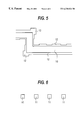
- FIG. 5 is a final reticle layout based on the modified reticle layout of FIG. 3A, from which areas of overlap have been removed;
- FIG. 6 is a final reticle layout based on the alignment budget-containing reticle layout of FIG. 4, from which all alignment budget borders have been removed;
- FIG. 7 is a schematic diagram of a computer system in which the process of the present invention can be implemented.
- the present invention provides a method for designing reticles which can be used to produce circuit designs having densely packed circuit features, in which alignment budgets are taken into account, in which the occurrence of printing errors is reduced or eliminated, and in which the variance between the actual exposure pattern and the desired exposure pattern is reduced.
- the present invention also provides a method for designing such reticles in which processing budgets are also taken into account.
- FIG. 1 is a partial schematic view of a circuit layout for a single layer of a semiconductor device.
- a conductive feature 10 e.g., a digitline
- contacts 11 e.g., interconnects
- a vertical direction i.e., perpendicular to the major axes of the layer.
- a common way of manufacturing such a layer is to first form the conductive feature 10 by patterning using a first reticle (not shown) and later form the contacts 11 , which pass through at least several layers, but which are designed to not be in electrical communication with the conductive feature 10 , using a second reticle.
- the present invention addresses problems which have occurred in the past with regard to aligning such features, despite the fact that they are formed at different times using different reticles, and despite the fact that the different reticles may not be aligned in precisely the same position relative to the stepper.
- the circuit layout for the layer is conceptually divided into two circuit layout portions, one for the reticle which will be used to pattern the conductive feature 10 (depicted in FIG. 2A) and one for the reticle which will be used to pattern the contacts 11 (depicted in FIG. 2 B).
- Each initial reticle layout includes printable reticle features which are sized, shaped and positioned similarly to the corresponding circuit features, with each printable reticle feature corresponding to a separate circuit feature in the circuit layout.
- a first initial reticle layout includes the conductive feature 10
- a second initial reticle layout includes the contacts 11 .
- One or more of the initial reticle layout portions is then modified by any OPC technique to generate one or more modified reticle layout portions such that if exposure were directed through a reticle having such a modified reticle layout onto a resist, the resist would be exposed in a pattern which includes features which more closely approximate the corresponding features in the circuit layout.
- the one or more modified reticle layout portions may be generated using any known technique, for instance, be generated completely through trial and error, through experience with particular reticle layouts, or by using one of the many known OPC algorithms.
- the generation of the modified reticle layout portions according to the present invention is not limited to any particular method or algorithm.
- the conductive feature 10 of the initial reticle layout portion is modified according to an OPC algorithm to generate a modified reticle layout.
- the modified reticle layout portion includes the conductive feature 10 plus correction areas 12 .
- At least one of the initial reticle layouts and/or at least one of the modified reticle layouts is then modified by adding an alignment budget border around the outside of each reticle feature contained in the reticle layout to generate one or more corresponding alignment budget-containing reticle layout.
- the width of the one or more alignment budget borders is determined based on the alignment budget for the apparatus being used, i.e., based on the maximum tolerable distance that printable reticle features on different reticles can be shifted relative to one another when placed in the stepper or steppers being used.
- the size of an alignment budget can be determined through calculation or through empirical study.
- a representative example of a suitable alignment budget is on the order of 70 nanometers.
- alignment budget areas are added to only one of each pair of adjacent reticle features which are to be patterned using different reticles.
- the contacts 11 are modified by adding alignment budget borders to generate an alignment budget-containing reticle layout.
- the alignment budget-containing reticle layout includes the contacts 11 plus alignment budget borders 13 .
- the contacts 11 are not modified to generate a modified reticle layout portion, but the present invention would encompass embodiments where the contacts 11 are modified according to any OPC technique. Any such OPC correction, if employed, is preferably completed before adding the alignment budget borders 13 .
- Each of the reticle layouts for the layer under consideration each of which may have been modified by addition of correction area and/or modified by addition of an alignment budget border, or which may have not been modified at all, are then laid over one another to check for any overlap between any correction areas corresponding to one feature and any alignment budget border areas corresponding to any other feature. If any such overlap exists, such overlap is deleted from the correction area to form a pre-final reticle layout for each reticle.
- FIG. 4 shows the modified reticle layout shown in FIG. 3A overlaid on the alignment budget-containing reticle layout shown in FIG. 3 B.
- the overlay shown in FIG. 4 includes the conductive feature 10 , contacts 11 , correction areas 12 and alignment budget borders 13 .
- FIG. 4 shows areas of overlap 14 where the alignment budget borders 13 overlap the correction areas 12 . In accordance with the present invention, such areas of overlap 14 are deleted from the correction areas 12 .
- FIG. 5 is a pre-final reticle layout based on the modified reticle layout of FIG. 3A, from which areas of overlap 14 , as shown in FIG. 4, have been removed. Since the alignment budget-containing reticle layout shown in FIG. 3B has no correction areas, the pre-final reticle layout for this reticle is the same as the layout in FIG. 3 B.
- FIG. 6 is a final reticle layout based on the pre-final reticle layout of FIG. 3B, from which the alignment budget borders 13 have been removed. Since the pre-final reticle layout of FIG. 5 has no alignment budget borders, the final reticle layout for this reticle is the same as the layout in FIG. 5 .
- the final reticle layouts are then sent to a mask shop, where reticles are manufactured according to the final reticle layouts.
- the present invention provides methods of forming reticles as described above, in which processing budgets are included in the alignment budgets described above.
- the width of any such processing budget is preferably determined through empirical study (e.g., by performing a number of etching steps and analyzing the maximum degree of variance of actual etching from a pattern in a resist through which the etchant is supplied.
- processing budgets can be determined by any other method, e.g., by calculation or through comparison with other known processing budgets.
- Such processing budgets are added to the alignment budget when determining the size of the borders 13 in, for example, the FIG. 3B layout.
- the present invention is also directed to phase shift masks, including attenuated phase shift masks.
- phase shift masks if the conductive feature(s) 10 , the contact(s) 11 and the correction area(s) 12 are formed of a transparent material, the remaining areas would be formed of a phase shift material, and vice-versa.
- the final reticle layout is preferably checked to analyze differences between the circuit layout and the pattern that will be produced on a resist by exposure through a reticle formed according to the corresponding final reticle layout.
- additional modifications can be made to the final reticle layout by repeating the procedure described above.
- Such additional modifications may include further changes generated by an OPC technique, re-inserting alignment budget borders, removing any areas of overlap, and removal of the alignment budget borders.
- simulation software that can be used to determine the pattern which will be produced on a resist by exposure through a reticle formed according to the final reticle layout include FAIM by Vector Technologies of Boston, Mass., SPLAT by the University of Berkeley, Calif. and PROLITH by Finle Technologies of Piano, Tex.
- the simulated image data can then be fed to a design rule checker or data integrity verification and correction program where it is compared to the data comprising the desired circuit feature layout. If the simulated image correlates with the circuit layout within predetermined parameters or design rules, the final reticle layout is then sent to a mask shop for manufacture of a reticle corresponding to the final reticle layout.
- the simulated image differs from the desired circuit feature layout by more than the design limits, further modifications may be made to the final reticle layout to counteract the areas of excessive variance from the circuit layout.
- the further modified reticle layout can then be run through the simulation and checking software again to check for excessive variances. These steps can be repeated until the simulated images correlate with the circuit layout within the design limits.
- design rule checker programs can be used to perform the data integrity verification and correction analysis.
- suitable software include CATS by Transcription Enterprises Limited of Los Gatos, Calif., iv Verify by Cadence System Inc. of San Jose, Calif., CheckMate by Mentor Graphics, Wilsonville, Oreg. and VeriCheck by Integrated Silicon System of Research Triangle Park, N.C.
- a preferred material for use in making the transparent portions of a reticle is quartz, however, any suitable transparent material, e.g., soda-lime glass, borosilicate glass, or other similar natural or synthetic substances can be used. Those of skill in the art can readily select an appropriate material for use in making the transparent portions of a reticle.
- a preferred material for use in making opaque portions (if present) of a reticle is chrome, however, any suitable opaque material can be used. Those of skill in the art can readily select an appropriate material for use in making the opaque portions of a reticle.
- phase shifting portions if present
- phase shifting attenuating portions if present
- a preferred material for use in making an attenuated phase shifting layer is molybdenum silicide (MoSi), however, any suitable partially light transmissive, phase shifting material can be used.
- MoSi molybdenum silicide
- Another material which has been used to form attenuated phase shifting layers is a leaky chrome, which is a mixture of chrome, nitrogen and oxygen.
- the present invention is further directed to any sequence of process steps which includes performance of any of the processes in accordance with the present invention, in addition to any other process steps, including but not limited to coating or applying one or more additional layers, removing part of all of one or more additional layers, creating a pattern on a surface of a layer by applying, exposing and developing a photoresist and then removing portions of the layer defined by the pattern, forming interconnect holes through two or more layers, creating interconnects, etc.
- FIGS. 1-6 relate to a very simple circuit layout. As indicated above, the present invention is applicable in like manner to any circuit layout, as will be readily appreciated by those skilled in the art.
- the correction areas are inserted before the alignment budget borders are inserted.
- the insertions of these areas can be carried out in any order, or any particular insertions can be carried out simultaneously.
- one or more correction areas could be added, followed by the insertion of one or more alignment budget borders, followed by the insertion of one or more correction areas, followed by the insertion of one or more alignment budget borders, followed by the simultaneous insertion of one or more correction areas and one or more alignment budget borders, etc.
- a circuit feature is provided with one or more correction areas as well as an alignment budget border, it is preferred that the correction areas be inserted before the alignment budget is inserted.
- FIG. 7 depicts an example of a computer system 650 in which a process according to the present invention can be implemented.
- the system 650 includes a central processing unit (CPU) 652 that communicates with an input/output (I/O) device 654 over a bus 670 .
- I/O input/output
- the computer system 650 also includes random access memory (RAM), read only memory (ROM) 660 and may include peripheral devices such as a floppy disk drive 664 or a compact disk read only memory (CD-ROM) drive 666 that also communicate with the CPU 652 over the bus 670 .
- RAM random access memory
- ROM read only memory
- CD-ROM compact disk read only memory
- the exact architecture of the computer system 650 is not critical, and any suitable combination of computer compatible devices may be incorporated into the system 650 .
- the computer system 650 is a UNIX based workstation.
- the program implementing the process of the present invention may be stored in ROM 608 , a CD-ROM 668 , a floppy disk 664 , a hard disk drive, or any other medium capable of storing a computer program and data required by the program.
- the computer program or programs used in the process of the present invention may be transmitted over a communications network as downloaded, for example, transmitted from a server computer or another computer connected to the computer system 650 which downloads the program or programs.
- the process of the present invention can be executed in a distributed manner over several computer systems 650 , whether connected by a network or not, to process different tasks associated with formation of a reticle, in parallel fashion.
- One or more of the features contained in the devices shown in FIG. 7 can be made using reticles designed in accordance with the present invention.
Abstract
Description
Claims (60)
Priority Applications (1)
| Application Number | Priority Date | Filing Date | Title |
|---|---|---|---|
| US09/386,314 US6238824B1 (en) | 1999-08-31 | 1999-08-31 | Method for designing and making photolithographic reticle, reticle, and photolithographic process |
Applications Claiming Priority (1)
| Application Number | Priority Date | Filing Date | Title |
|---|---|---|---|
| US09/386,314 US6238824B1 (en) | 1999-08-31 | 1999-08-31 | Method for designing and making photolithographic reticle, reticle, and photolithographic process |
Publications (1)
| Publication Number | Publication Date |
|---|---|
| US6238824B1 true US6238824B1 (en) | 2001-05-29 |
Family
ID=23525084
Family Applications (1)
| Application Number | Title | Priority Date | Filing Date |
|---|---|---|---|
| US09/386,314 Expired - Lifetime US6238824B1 (en) | 1999-08-31 | 1999-08-31 | Method for designing and making photolithographic reticle, reticle, and photolithographic process |
Country Status (1)
| Country | Link |
|---|---|
| US (1) | US6238824B1 (en) |
Cited By (25)
| Publication number | Priority date | Publication date | Assignee | Title |
|---|---|---|---|---|
| US20020010906A1 (en) * | 2000-06-13 | 2002-01-24 | Kabushiki Kaisha Toshiba | Circuit pattern design method,exposure method, charged-particle beam exposure system |
| US6403477B1 (en) * | 1999-10-25 | 2002-06-11 | Nec Corporation | Method for correcting an optical proximity effect in an interconnect pattern by shortening the legs of cutout patterns to avoid linewidth reduction |
| US20020152454A1 (en) * | 2000-07-05 | 2002-10-17 | Numerical Technologies, Inc. | Design data format and hierarchy management for processing |
| US20020155363A1 (en) * | 2000-07-05 | 2002-10-24 | Numerical Technologies, Inc. | Standard cell design incorporating phase information |
| US20030024899A1 (en) * | 2001-08-02 | 2003-02-06 | Fujitsu Limited | Exposure method utilizing optical proximity corrected exposure patterns, an apparatus for generating optical proximity corrected exposure data, and an exposure apparatus for optical proximity corrected exposure data |
| US20030061596A1 (en) * | 2001-09-25 | 2003-03-27 | Canon Kabushiki Kaisha | Exposure apparatus, method of controlling same, and method of manufacturing devices |
| US20030126582A1 (en) * | 2001-12-27 | 2003-07-03 | Sachiko Kobayashi | Pattern correction method and manufacturing method of semiconductor device |
| US6598217B1 (en) * | 2000-02-18 | 2003-07-22 | Mitsubishi Denki Kabushiki Kaisha | Method of mounting fabrication-historical data for semiconductor device, and semiconductor device fabricated by such a method |
| US20030137886A1 (en) * | 2001-11-15 | 2003-07-24 | Numerical Technologies, Inc. | Cutting patterns for full phase shifting masks |
| US6604234B2 (en) * | 2000-05-26 | 2003-08-05 | Hitachi, Ltd. | Method of designing/manufacturing semiconductor integrated circuit device using combined exposure pattern and semiconductor integrated circuit device |
| US6605816B2 (en) * | 2000-09-18 | 2003-08-12 | Micronic Laser Systems Ab | Reticle and direct lithography writing strategy |
| US6620561B2 (en) * | 2000-04-27 | 2003-09-16 | Micron Technology Inc | Method for designing photolithographic reticle layout, reticle, and photolithographic process |
| US20030208742A1 (en) * | 2001-07-10 | 2003-11-06 | Lacour Patrick Joseph | Space classification for resolution enhancement techniques |
| US20040031013A1 (en) * | 2002-08-06 | 2004-02-12 | Dulman H. Daniel | Methods of forming patterned reticles |
| US6803157B2 (en) | 2002-03-01 | 2004-10-12 | Micron Technology, Inc. | Pattern mask with features to minimize the effect of aberrations |
| DE10340611A1 (en) * | 2003-08-29 | 2005-03-24 | Infineon Technologies Ag | Lithographic mask for making integrated semiconductor circuit by photolithographic process, comprising angular structure element formed by two opaque segments, with adjacent transparent structure at convex section of angular structure |
| US20050125763A1 (en) * | 2003-06-30 | 2005-06-09 | Taiwan Semiconductor Manufacturing Company, Ltd. | System and method for the online design of a reticle field layout |
| US6931618B1 (en) | 2002-01-16 | 2005-08-16 | Advanced Micro Devices, Inc. | Feed forward process control using scatterometry for reticle fabrication |
| US20050251771A1 (en) * | 2004-05-07 | 2005-11-10 | Mentor Graphics Corporation | Integrated circuit layout design methodology with process variation bands |
| US20090019419A1 (en) * | 1999-03-04 | 2009-01-15 | Matsushita Electric Industrial Co., Ltd. | Method for forming LSI pattern |
| US20100017779A1 (en) * | 2008-07-17 | 2010-01-21 | Hynix Semiconductor Inc. | Method for Decomposing Designed Pattern Layout and Method for Fabricating Exposure Mask Using the Same |
| US20100112462A1 (en) * | 2008-11-05 | 2010-05-06 | Micron Technology, Inc. | Reticles with subdivided blocking regions |
| US20110186333A1 (en) * | 2009-08-05 | 2011-08-04 | Zhigang Wang | Printed Compatible Designs and Layout Schemes for Printed Electronics |
| US20120144351A1 (en) * | 2006-11-09 | 2012-06-07 | Mentor Graphics Corporation | Analysis optimzer |
| US8656320B2 (en) * | 2012-07-12 | 2014-02-18 | Stmicroelectronics (Crolles 2) Sas | Method for creating a photolithography mask |
Citations (5)
| Publication number | Priority date | Publication date | Assignee | Title |
|---|---|---|---|---|
| US5475766A (en) | 1991-09-05 | 1995-12-12 | Kabushiki Kaisha Toshiba | Pattern inspection apparatus with corner rounding of reference pattern data |
| US5723233A (en) | 1996-02-27 | 1998-03-03 | Lsi Logic Corporation | Optical proximity correction method and apparatus |
| US5847421A (en) | 1996-07-15 | 1998-12-08 | Kabushiki Kaisha Toshiba | Logic cell having efficient optical proximity effect correction |
| US5900338A (en) * | 1996-02-27 | 1999-05-04 | Lsi Logic Corporation | Performing optical proximity correction with the aid of design rule checkers |
| US5917932A (en) * | 1997-06-24 | 1999-06-29 | International Business Machines Corporation | System and method for evaluating image placement on pre-distorted masks |
-
1999
- 1999-08-31 US US09/386,314 patent/US6238824B1/en not_active Expired - Lifetime
Patent Citations (5)
| Publication number | Priority date | Publication date | Assignee | Title |
|---|---|---|---|---|
| US5475766A (en) | 1991-09-05 | 1995-12-12 | Kabushiki Kaisha Toshiba | Pattern inspection apparatus with corner rounding of reference pattern data |
| US5723233A (en) | 1996-02-27 | 1998-03-03 | Lsi Logic Corporation | Optical proximity correction method and apparatus |
| US5900338A (en) * | 1996-02-27 | 1999-05-04 | Lsi Logic Corporation | Performing optical proximity correction with the aid of design rule checkers |
| US5847421A (en) | 1996-07-15 | 1998-12-08 | Kabushiki Kaisha Toshiba | Logic cell having efficient optical proximity effect correction |
| US5917932A (en) * | 1997-06-24 | 1999-06-29 | International Business Machines Corporation | System and method for evaluating image placement on pre-distorted masks |
Cited By (71)
| Publication number | Priority date | Publication date | Assignee | Title |
|---|---|---|---|---|
| US20090019419A1 (en) * | 1999-03-04 | 2009-01-15 | Matsushita Electric Industrial Co., Ltd. | Method for forming LSI pattern |
| US8095894B2 (en) * | 1999-03-04 | 2012-01-10 | Panasonic Corporation | Changing a design rule for forming LSI pattern based on evaluating effectiveness of optical proximity corrected patterns |
| US6403477B1 (en) * | 1999-10-25 | 2002-06-11 | Nec Corporation | Method for correcting an optical proximity effect in an interconnect pattern by shortening the legs of cutout patterns to avoid linewidth reduction |
| US6598217B1 (en) * | 2000-02-18 | 2003-07-22 | Mitsubishi Denki Kabushiki Kaisha | Method of mounting fabrication-historical data for semiconductor device, and semiconductor device fabricated by such a method |
| US6620561B2 (en) * | 2000-04-27 | 2003-09-16 | Micron Technology Inc | Method for designing photolithographic reticle layout, reticle, and photolithographic process |
| US6604234B2 (en) * | 2000-05-26 | 2003-08-05 | Hitachi, Ltd. | Method of designing/manufacturing semiconductor integrated circuit device using combined exposure pattern and semiconductor integrated circuit device |
| US6481004B2 (en) * | 2000-06-13 | 2002-11-12 | Kabushiki Kaisha Toshiba | Circuit pattern design method, exposure method, charged-particle beam exposure system |
| US20020010906A1 (en) * | 2000-06-13 | 2002-01-24 | Kabushiki Kaisha Toshiba | Circuit pattern design method,exposure method, charged-particle beam exposure system |
| US7028285B2 (en) | 2000-07-05 | 2006-04-11 | Synopsys, Inc. | Standard cell design incorporating phase information |
| US20050166173A1 (en) * | 2000-07-05 | 2005-07-28 | Synopsys, Inc. | Design data format and hierarchy management for processing |
| US7500217B2 (en) | 2000-07-05 | 2009-03-03 | Synopsys, Inc. | Handling of flat data for phase processing including growing shapes within bins to identify clusters |
| US20020155363A1 (en) * | 2000-07-05 | 2002-10-24 | Numerical Technologies, Inc. | Standard cell design incorporating phase information |
| US20020152454A1 (en) * | 2000-07-05 | 2002-10-17 | Numerical Technologies, Inc. | Design data format and hierarchy management for processing |
| US8977989B2 (en) | 2000-07-05 | 2015-03-10 | Synopsys, Inc. | Handling of flat data for phase processing including growing shapes within bins to identify clusters |
| US6978436B2 (en) * | 2000-07-05 | 2005-12-20 | Synopsys, Inc. | Design data format and hierarchy management for phase processing |
| US20080131821A1 (en) * | 2000-09-18 | 2008-06-05 | Micronic Laser Systems Ab | Dual layer workpiece masking and manufacturing process |
| US6605816B2 (en) * | 2000-09-18 | 2003-08-12 | Micronic Laser Systems Ab | Reticle and direct lithography writing strategy |
| US7588870B2 (en) | 2000-09-18 | 2009-09-15 | Micronic Laser Systems Ab | Dual layer workpiece masking and manufacturing process |
| US6799313B2 (en) * | 2001-07-10 | 2004-09-28 | Lacour Patrick Joseph | Space classification for resolution enhancement techniques |
| US20030208742A1 (en) * | 2001-07-10 | 2003-11-06 | Lacour Patrick Joseph | Space classification for resolution enhancement techniques |
| JP2003043664A (en) * | 2001-08-02 | 2003-02-13 | Fujitsu Ltd | Exposing method using optical proximity corrected exposure pattern, generating device for optical proximity corrected exposure data, and exposing device for light-proximity corrected exposure data |
| US6968531B2 (en) * | 2001-08-02 | 2005-11-22 | Fujitsu Limited | Exposure method utilizing optical proximity corrected exposure patterns, an apparatus for generating optical proximity corrected exposure data, and an exposure apparatus for optical proximity corrected exposure data |
| JP4615156B2 (en) * | 2001-08-02 | 2011-01-19 | 富士通セミコンダクター株式会社 | EXPOSURE METHOD USING EXPOSURE PATTERN COMPRISED WITH OPTICAL PROXIMITY, EXPOSURE DATA GENERATION APPARATUS FOR OPTICAL PROXIMITY CORRECTION, AND EXPOSURE APPARATUS FOR EXPOSURE DATA COMPACTED WITH OPTICAL PROXIMITY |
| US20030024899A1 (en) * | 2001-08-02 | 2003-02-06 | Fujitsu Limited | Exposure method utilizing optical proximity corrected exposure patterns, an apparatus for generating optical proximity corrected exposure data, and an exposure apparatus for optical proximity corrected exposure data |
| US20030061596A1 (en) * | 2001-09-25 | 2003-03-27 | Canon Kabushiki Kaisha | Exposure apparatus, method of controlling same, and method of manufacturing devices |
| US20030137886A1 (en) * | 2001-11-15 | 2003-07-24 | Numerical Technologies, Inc. | Cutting patterns for full phase shifting masks |
| US6981240B2 (en) | 2001-11-15 | 2005-12-27 | Synopsys, Inc. | Cutting patterns for full phase shifting masks |
| US7065739B2 (en) * | 2001-12-27 | 2006-06-20 | Kabushiki Kaisha Toshiba | Pattern correction method of semiconductor device |
| US20060190921A1 (en) * | 2001-12-27 | 2006-08-24 | Kabushiki Kaisha Toshiba | Manufacturing Method of Semiconductor Device |
| US20030126582A1 (en) * | 2001-12-27 | 2003-07-03 | Sachiko Kobayashi | Pattern correction method and manufacturing method of semiconductor device |
| US7509623B2 (en) | 2001-12-27 | 2009-03-24 | Kabushiki Kaisha Toshiba | Manufacturing method of semiconductor device |
| US6931618B1 (en) | 2002-01-16 | 2005-08-16 | Advanced Micro Devices, Inc. | Feed forward process control using scatterometry for reticle fabrication |
| US6803157B2 (en) | 2002-03-01 | 2004-10-12 | Micron Technology, Inc. | Pattern mask with features to minimize the effect of aberrations |
| US20050003281A1 (en) * | 2002-03-01 | 2005-01-06 | Micron Technology, Inc. A Corporation Of Delaware | Pattern mask with features to minimize the effect of aberrations |
| US7105278B2 (en) | 2002-03-01 | 2006-09-12 | Micron Technology, Inc. | Pattern mask with features to minimize the effect of aberrations |
| US20060093927A1 (en) * | 2002-03-01 | 2006-05-04 | Pary Baluswamy | Pattern mask with features to minimize the effect of aberrations |
| US7073161B2 (en) | 2002-08-06 | 2006-07-04 | Micron Technology, Inc. | Methods of forming patterned reticles |
| US20050008952A1 (en) * | 2002-08-06 | 2005-01-13 | Dulman H. Daniel | Methods of forming patterned reticles |
| US7086031B2 (en) | 2002-08-06 | 2006-08-01 | Micron Technology, Inc. | Methods of forming patterned reticles |
| US7093227B2 (en) | 2002-08-06 | 2006-08-15 | Micron Technology, Inc. | Methods of forming patterned reticles |
| US20040031013A1 (en) * | 2002-08-06 | 2004-02-12 | Dulman H. Daniel | Methods of forming patterned reticles |
| US7107572B2 (en) | 2002-08-06 | 2006-09-12 | Micron Technology, Inc. | Methods of forming patterned reticles |
| US6842889B2 (en) * | 2002-08-06 | 2005-01-11 | Micron Technology, Inc. | Methods of forming patterned reticles |
| US7350182B2 (en) | 2002-08-06 | 2008-03-25 | Micron Technology, Inc. | Methods of forming patterned reticles |
| US20050008949A1 (en) * | 2002-08-06 | 2005-01-13 | Dulman H. Daniel | Methods of forming patterned reticles |
| US20050008953A1 (en) * | 2002-08-06 | 2005-01-13 | Dulman H. Daniel | Methods of forming patterned reticles |
| US20050008951A1 (en) * | 2002-08-06 | 2005-01-13 | Dulman H. Daniel | Methods of forming patterned reticles |
| US20050008950A1 (en) * | 2002-08-06 | 2005-01-13 | Dulman H. Daniel | Methods of forming patterned reticles |
| US20050125763A1 (en) * | 2003-06-30 | 2005-06-09 | Taiwan Semiconductor Manufacturing Company, Ltd. | System and method for the online design of a reticle field layout |
| US7354683B2 (en) | 2003-08-29 | 2008-04-08 | Infineon Technologies Ag | Lithography mask for imaging of convex structures |
| DE10340611B4 (en) * | 2003-08-29 | 2007-08-23 | Infineon Technologies Ag | Lithography mask for imaging convex structures |
| DE10340611A1 (en) * | 2003-08-29 | 2005-03-24 | Infineon Technologies Ag | Lithographic mask for making integrated semiconductor circuit by photolithographic process, comprising angular structure element formed by two opaque segments, with adjacent transparent structure at convex section of angular structure |
| US20050095512A1 (en) * | 2003-08-29 | 2005-05-05 | Molela Moukara | Lithography mask for imaging of convex structures |
| US20050251771A1 (en) * | 2004-05-07 | 2005-11-10 | Mentor Graphics Corporation | Integrated circuit layout design methodology with process variation bands |
| US9977856B2 (en) | 2004-05-07 | 2018-05-22 | Mentor Graphics Corporation | Integrated circuit layout design methodology with process variation bands |
| US9361424B2 (en) | 2004-05-07 | 2016-06-07 | Mentor Graphics Corporation | Integrated circuit layout design methodology with process variation bands |
| US8799830B2 (en) | 2004-05-07 | 2014-08-05 | Mentor Graphics Corporation | Integrated circuit layout design methodology with process variation bands |
| US8504959B2 (en) * | 2006-11-09 | 2013-08-06 | Mentor Graphics Corporation | Analysis optimizer |
| US8832609B2 (en) | 2006-11-09 | 2014-09-09 | Mentor Graphics Corporation | Analysis optimizer |
| US20120144351A1 (en) * | 2006-11-09 | 2012-06-07 | Mentor Graphics Corporation | Analysis optimzer |
| US20100017779A1 (en) * | 2008-07-17 | 2010-01-21 | Hynix Semiconductor Inc. | Method for Decomposing Designed Pattern Layout and Method for Fabricating Exposure Mask Using the Same |
| US8429587B2 (en) | 2008-07-17 | 2013-04-23 | Hynix Semiconductor Inc. | Method for decomposing a designed pattern layout |
| US8151222B2 (en) * | 2008-07-17 | 2012-04-03 | Hynix Semiconductor Inc. | Method for decomposing designed pattern layout and method for fabricating exposure mask using the same |
| US8383301B2 (en) | 2008-11-05 | 2013-02-26 | Micron Technology, Inc. | Methods of fabricating reticles with subdivided blocking regions |
| US8822108B2 (en) | 2008-11-05 | 2014-09-02 | Micron Technology, Inc. | Reticles with subdivided blocking regions |
| US8071262B2 (en) | 2008-11-05 | 2011-12-06 | Micron Technology, Inc. | Reticles with subdivided blocking regions |
| US20100112462A1 (en) * | 2008-11-05 | 2010-05-06 | Micron Technology, Inc. | Reticles with subdivided blocking regions |
| US8383952B2 (en) * | 2009-08-05 | 2013-02-26 | Kovio, Inc. | Printed compatible designs and layout schemes for printed electronics |
| US9155202B2 (en) | 2009-08-05 | 2015-10-06 | Thin Film Electronics Asa | Print compatible designs and layout schemes for printed electronics |
| US20110186333A1 (en) * | 2009-08-05 | 2011-08-04 | Zhigang Wang | Printed Compatible Designs and Layout Schemes for Printed Electronics |
| US8656320B2 (en) * | 2012-07-12 | 2014-02-18 | Stmicroelectronics (Crolles 2) Sas | Method for creating a photolithography mask |
Similar Documents
| Publication | Publication Date | Title |
|---|---|---|
| US6238824B1 (en) | Method for designing and making photolithographic reticle, reticle, and photolithographic process | |
| US5801954A (en) | Process for designing and checking a mask layout | |
| US6413684B1 (en) | Method to eliminate side lobe printing of attenuated phase shift masks | |
| US6185727B1 (en) | Design verification for asymmetric phase shift mask layouts | |
| US7147976B2 (en) | Binary OPC for assist feature layout optimization | |
| US7765515B2 (en) | Pattern match based optical proximity correction and verification of integrated circuit layout | |
| US7172838B2 (en) | Chromeless phase mask layout generation | |
| US8832609B2 (en) | Analysis optimizer | |
| US20060200790A1 (en) | Model-based SRAF insertion | |
| US7010775B2 (en) | Method for creating mask pattern for circuit fabrication and method for verifying mask pattern for circuit fabrication | |
| US20090007053A1 (en) | Method of Manufacturing Mask for Semiconductor Device | |
| US6465138B1 (en) | Method for designing and making photolithographic reticle, reticle, and photolithographic process | |
| US7458060B2 (en) | Yield-limiting design-rules-compliant pattern library generation and layout inspection | |
| US6472108B1 (en) | Optical proximity correction method | |
| US7107572B2 (en) | Methods of forming patterned reticles | |
| US6664010B2 (en) | OPC method for generating corrected patterns for a phase-shifting mask and its trimming mask and associated device and integrated circuit configuration | |
| US20070111112A1 (en) | Systems and methods for fabricating photo masks | |
| US6782525B2 (en) | Wafer process critical dimension, alignment, and registration analysis simulation tool | |
| US20090281778A1 (en) | Method and system for identifying weak points in an integrated circuit design | |
| US6401236B1 (en) | Method to eliminate side lobe printing of attenuated phase shift | |
| US7039896B2 (en) | Gradient method of mask edge correction | |
| US20090276735A1 (en) | System and Method of Correcting Errors in SEM-Measurements | |
| US7251806B2 (en) | Model-based two-dimensional interpretation filtering | |
| Sahouria et al. | Full-chip process simulation for silicon DRC | |
| US8713487B2 (en) | Sub-resolution assist feature repair |
Legal Events
| Date | Code | Title | Description |
|---|---|---|---|
| AS | Assignment |
Owner name: MICRON TECHNOLOGY, IDAHO Free format text: ASSIGNMENT OF ASSIGNORS INTEREST;ASSIGNORS:FUTRELL, JOHN R.;PIERRAT, CHRISTOPHE;STANTON, WILLIAM;REEL/FRAME:010383/0951;SIGNING DATES FROM 19990831 TO 19991013 |
|
| STCF | Information on status: patent grant |
Free format text: PATENTED CASE |
|
| FPAY | Fee payment |
Year of fee payment: 4 |
|
| FEPP | Fee payment procedure |
Free format text: PAYER NUMBER DE-ASSIGNED (ORIGINAL EVENT CODE: RMPN); ENTITY STATUS OF PATENT OWNER: LARGE ENTITY Free format text: PAYOR NUMBER ASSIGNED (ORIGINAL EVENT CODE: ASPN); ENTITY STATUS OF PATENT OWNER: LARGE ENTITY |
|
| FPAY | Fee payment |
Year of fee payment: 8 |
|
| FPAY | Fee payment |
Year of fee payment: 12 |
|
| AS | Assignment |
Owner name: U.S. BANK NATIONAL ASSOCIATION, AS COLLATERAL AGENT, CALIFORNIA Free format text: SECURITY INTEREST;ASSIGNOR:MICRON TECHNOLOGY, INC.;REEL/FRAME:038669/0001 Effective date: 20160426 Owner name: U.S. BANK NATIONAL ASSOCIATION, AS COLLATERAL AGEN Free format text: SECURITY INTEREST;ASSIGNOR:MICRON TECHNOLOGY, INC.;REEL/FRAME:038669/0001 Effective date: 20160426 |
|
| AS | Assignment |
Owner name: MORGAN STANLEY SENIOR FUNDING, INC., AS COLLATERAL AGENT, MARYLAND Free format text: PATENT SECURITY AGREEMENT;ASSIGNOR:MICRON TECHNOLOGY, INC.;REEL/FRAME:038954/0001 Effective date: 20160426 Owner name: MORGAN STANLEY SENIOR FUNDING, INC., AS COLLATERAL Free format text: PATENT SECURITY AGREEMENT;ASSIGNOR:MICRON TECHNOLOGY, INC.;REEL/FRAME:038954/0001 Effective date: 20160426 |
|
| AS | Assignment |
Owner name: U.S. BANK NATIONAL ASSOCIATION, AS COLLATERAL AGENT, CALIFORNIA Free format text: CORRECTIVE ASSIGNMENT TO CORRECT THE REPLACE ERRONEOUSLY FILED PATENT #7358718 WITH THE CORRECT PATENT #7358178 PREVIOUSLY RECORDED ON REEL 038669 FRAME 0001. ASSIGNOR(S) HEREBY CONFIRMS THE SECURITY INTEREST;ASSIGNOR:MICRON TECHNOLOGY, INC.;REEL/FRAME:043079/0001 Effective date: 20160426 Owner name: U.S. BANK NATIONAL ASSOCIATION, AS COLLATERAL AGEN Free format text: CORRECTIVE ASSIGNMENT TO CORRECT THE REPLACE ERRONEOUSLY FILED PATENT #7358718 WITH THE CORRECT PATENT #7358178 PREVIOUSLY RECORDED ON REEL 038669 FRAME 0001. ASSIGNOR(S) HEREBY CONFIRMS THE SECURITY INTEREST;ASSIGNOR:MICRON TECHNOLOGY, INC.;REEL/FRAME:043079/0001 Effective date: 20160426 |
|
| AS | Assignment |
Owner name: JPMORGAN CHASE BANK, N.A., AS COLLATERAL AGENT, ILLINOIS Free format text: SECURITY INTEREST;ASSIGNORS:MICRON TECHNOLOGY, INC.;MICRON SEMICONDUCTOR PRODUCTS, INC.;REEL/FRAME:047540/0001 Effective date: 20180703 Owner name: JPMORGAN CHASE BANK, N.A., AS COLLATERAL AGENT, IL Free format text: SECURITY INTEREST;ASSIGNORS:MICRON TECHNOLOGY, INC.;MICRON SEMICONDUCTOR PRODUCTS, INC.;REEL/FRAME:047540/0001 Effective date: 20180703 |
|
| AS | Assignment |
Owner name: MICRON TECHNOLOGY, INC., IDAHO Free format text: RELEASE BY SECURED PARTY;ASSIGNOR:U.S. BANK NATIONAL ASSOCIATION, AS COLLATERAL AGENT;REEL/FRAME:047243/0001 Effective date: 20180629 |
|
| AS | Assignment |
Owner name: MICRON TECHNOLOGY, INC., IDAHO Free format text: RELEASE BY SECURED PARTY;ASSIGNOR:MORGAN STANLEY SENIOR FUNDING, INC., AS COLLATERAL AGENT;REEL/FRAME:050937/0001 Effective date: 20190731 |
|
| AS | Assignment |
Owner name: MICRON SEMICONDUCTOR PRODUCTS, INC., IDAHO Free format text: RELEASE BY SECURED PARTY;ASSIGNOR:JPMORGAN CHASE BANK, N.A., AS COLLATERAL AGENT;REEL/FRAME:051028/0001 Effective date: 20190731 Owner name: MICRON TECHNOLOGY, INC., IDAHO Free format text: RELEASE BY SECURED PARTY;ASSIGNOR:JPMORGAN CHASE BANK, N.A., AS COLLATERAL AGENT;REEL/FRAME:051028/0001 Effective date: 20190731 |