US6238982B1 - Multiple threshold voltage semiconductor device fabrication technology - Google Patents
Multiple threshold voltage semiconductor device fabrication technology Download PDFInfo
- Publication number
- US6238982B1 US6238982B1 US09/289,909 US28990999A US6238982B1 US 6238982 B1 US6238982 B1 US 6238982B1 US 28990999 A US28990999 A US 28990999A US 6238982 B1 US6238982 B1 US 6238982B1
- Authority
- US
- United States
- Prior art keywords
- gate
- implant
- channel
- regions
- forming
- Prior art date
- Legal status (The legal status is an assumption and is not a legal conclusion. Google has not performed a legal analysis and makes no representation as to the accuracy of the status listed.)
- Expired - Lifetime
Links
- 238000005516 engineering process Methods 0.000 title abstract description 7
- 238000005389 semiconductor device fabrication Methods 0.000 title 1
- 238000000034 method Methods 0.000 claims abstract description 50
- 239000007943 implant Substances 0.000 claims description 67
- 239000002019 doping agent Substances 0.000 claims description 33
- 239000000758 substrate Substances 0.000 claims description 32
- 238000004519 manufacturing process Methods 0.000 claims description 29
- 150000002500 ions Chemical class 0.000 claims description 17
- 239000004065 semiconductor Substances 0.000 claims description 17
- 229910052785 arsenic Inorganic materials 0.000 claims description 7
- 229910021420 polycrystalline silicon Inorganic materials 0.000 claims description 6
- 229920005591 polysilicon Polymers 0.000 claims description 6
- ZOXJGFHDIHLPTG-UHFFFAOYSA-N Boron Chemical compound [B] ZOXJGFHDIHLPTG-UHFFFAOYSA-N 0.000 claims description 5
- 229910021417 amorphous silicon Inorganic materials 0.000 claims description 5
- 229910052796 boron Inorganic materials 0.000 claims description 5
- 238000002513 implantation Methods 0.000 claims description 5
- RQNWIZPPADIBDY-UHFFFAOYSA-N arsenic atom Chemical compound [As] RQNWIZPPADIBDY-UHFFFAOYSA-N 0.000 claims description 4
- 238000002955 isolation Methods 0.000 claims description 4
- 230000003647 oxidation Effects 0.000 claims description 4
- 238000007254 oxidation reaction Methods 0.000 claims description 4
- OAICVXFJPJFONN-UHFFFAOYSA-N Phosphorus Chemical compound [P] OAICVXFJPJFONN-UHFFFAOYSA-N 0.000 claims description 3
- 229910052698 phosphorus Inorganic materials 0.000 claims description 3
- 239000011574 phosphorus Substances 0.000 claims description 3
- 239000010410 layer Substances 0.000 description 15
- XUIMIQQOPSSXEZ-UHFFFAOYSA-N Silicon Chemical compound [Si] XUIMIQQOPSSXEZ-UHFFFAOYSA-N 0.000 description 8
- 229910052710 silicon Inorganic materials 0.000 description 8
- 239000010703 silicon Substances 0.000 description 8
- 230000015572 biosynthetic process Effects 0.000 description 7
- 239000012535 impurity Substances 0.000 description 7
- 230000009977 dual effect Effects 0.000 description 6
- 125000006850 spacer group Chemical group 0.000 description 4
- -1 arsenic ions Chemical class 0.000 description 3
- 230000000694 effects Effects 0.000 description 3
- 239000000463 material Substances 0.000 description 3
- 239000000243 solution Substances 0.000 description 3
- 229910052581 Si3N4 Inorganic materials 0.000 description 2
- 239000010408 film Substances 0.000 description 2
- 230000006870 function Effects 0.000 description 2
- 238000002347 injection Methods 0.000 description 2
- 239000007924 injection Substances 0.000 description 2
- 238000012986 modification Methods 0.000 description 2
- 230000004048 modification Effects 0.000 description 2
- 238000001020 plasma etching Methods 0.000 description 2
- HQVNEWCFYHHQES-UHFFFAOYSA-N silicon nitride Chemical compound N12[Si]34N5[Si]62N3[Si]51N64 HQVNEWCFYHHQES-UHFFFAOYSA-N 0.000 description 2
- 239000002344 surface layer Substances 0.000 description 2
- 238000000151 deposition Methods 0.000 description 1
- 230000008021 deposition Effects 0.000 description 1
- 238000011161 development Methods 0.000 description 1
- 230000018109 developmental process Effects 0.000 description 1
- BABWHSBPEIVBBZ-UHFFFAOYSA-N diazete Chemical compound C1=CN=N1 BABWHSBPEIVBBZ-UHFFFAOYSA-N 0.000 description 1
- 238000005530 etching Methods 0.000 description 1
- 230000005669 field effect Effects 0.000 description 1
- BHEPBYXIRTUNPN-UHFFFAOYSA-N hydridophosphorus(.) (triplet) Chemical compound [PH] BHEPBYXIRTUNPN-UHFFFAOYSA-N 0.000 description 1
- 239000012774 insulation material Substances 0.000 description 1
- 229910044991 metal oxide Inorganic materials 0.000 description 1
- 150000004706 metal oxides Chemical class 0.000 description 1
- 238000007517 polishing process Methods 0.000 description 1
- 238000004151 rapid thermal annealing Methods 0.000 description 1
- 238000004544 sputter deposition Methods 0.000 description 1
- 239000010409 thin film Substances 0.000 description 1
Images


Classifications
-
- H—ELECTRICITY
- H01—ELECTRIC ELEMENTS
- H01L—SEMICONDUCTOR DEVICES NOT COVERED BY CLASS H10
- H01L29/00—Semiconductor devices adapted for rectifying, amplifying, oscillating or switching, or capacitors or resistors with at least one potential-jump barrier or surface barrier, e.g. PN junction depletion layer or carrier concentration layer; Details of semiconductor bodies or of electrodes thereof ; Multistep manufacturing processes therefor
- H01L29/02—Semiconductor bodies ; Multistep manufacturing processes therefor
- H01L29/06—Semiconductor bodies ; Multistep manufacturing processes therefor characterised by their shape; characterised by the shapes, relative sizes, or dispositions of the semiconductor regions ; characterised by the concentration or distribution of impurities within semiconductor regions
- H01L29/10—Semiconductor bodies ; Multistep manufacturing processes therefor characterised by their shape; characterised by the shapes, relative sizes, or dispositions of the semiconductor regions ; characterised by the concentration or distribution of impurities within semiconductor regions with semiconductor regions connected to an electrode not carrying current to be rectified, amplified or switched and such electrode being part of a semiconductor device which comprises three or more electrodes
- H01L29/1025—Channel region of field-effect devices
- H01L29/1029—Channel region of field-effect devices of field-effect transistors
- H01L29/1033—Channel region of field-effect devices of field-effect transistors with insulated gate, e.g. characterised by the length, the width, the geometric contour or the doping structure
- H01L29/1041—Channel region of field-effect devices of field-effect transistors with insulated gate, e.g. characterised by the length, the width, the geometric contour or the doping structure with a non-uniform doping structure in the channel region surface
- H01L29/1045—Channel region of field-effect devices of field-effect transistors with insulated gate, e.g. characterised by the length, the width, the geometric contour or the doping structure with a non-uniform doping structure in the channel region surface the doping structure being parallel to the channel length, e.g. DMOS like
-
- H—ELECTRICITY
- H01—ELECTRIC ELEMENTS
- H01L—SEMICONDUCTOR DEVICES NOT COVERED BY CLASS H10
- H01L21/00—Processes or apparatus adapted for the manufacture or treatment of semiconductor or solid state devices or of parts thereof
- H01L21/70—Manufacture or treatment of devices consisting of a plurality of solid state components formed in or on a common substrate or of parts thereof; Manufacture of integrated circuit devices or of parts thereof
- H01L21/77—Manufacture or treatment of devices consisting of a plurality of solid state components or integrated circuits formed in, or on, a common substrate
- H01L21/78—Manufacture or treatment of devices consisting of a plurality of solid state components or integrated circuits formed in, or on, a common substrate with subsequent division of the substrate into plural individual devices
- H01L21/82—Manufacture or treatment of devices consisting of a plurality of solid state components or integrated circuits formed in, or on, a common substrate with subsequent division of the substrate into plural individual devices to produce devices, e.g. integrated circuits, each consisting of a plurality of components
- H01L21/822—Manufacture or treatment of devices consisting of a plurality of solid state components or integrated circuits formed in, or on, a common substrate with subsequent division of the substrate into plural individual devices to produce devices, e.g. integrated circuits, each consisting of a plurality of components the substrate being a semiconductor, using silicon technology
- H01L21/8232—Field-effect technology
- H01L21/8234—MIS technology, i.e. integration processes of field effect transistors of the conductor-insulator-semiconductor type
- H01L21/823412—MIS technology, i.e. integration processes of field effect transistors of the conductor-insulator-semiconductor type with a particular manufacturing method of the channel structures, e.g. channel implants, halo or pocket implants, or channel materials
-
- H—ELECTRICITY
- H01—ELECTRIC ELEMENTS
- H01L—SEMICONDUCTOR DEVICES NOT COVERED BY CLASS H10
- H01L21/00—Processes or apparatus adapted for the manufacture or treatment of semiconductor or solid state devices or of parts thereof
- H01L21/70—Manufacture or treatment of devices consisting of a plurality of solid state components formed in or on a common substrate or of parts thereof; Manufacture of integrated circuit devices or of parts thereof
- H01L21/77—Manufacture or treatment of devices consisting of a plurality of solid state components or integrated circuits formed in, or on, a common substrate
- H01L21/78—Manufacture or treatment of devices consisting of a plurality of solid state components or integrated circuits formed in, or on, a common substrate with subsequent division of the substrate into plural individual devices
- H01L21/82—Manufacture or treatment of devices consisting of a plurality of solid state components or integrated circuits formed in, or on, a common substrate with subsequent division of the substrate into plural individual devices to produce devices, e.g. integrated circuits, each consisting of a plurality of components
- H01L21/822—Manufacture or treatment of devices consisting of a plurality of solid state components or integrated circuits formed in, or on, a common substrate with subsequent division of the substrate into plural individual devices to produce devices, e.g. integrated circuits, each consisting of a plurality of components the substrate being a semiconductor, using silicon technology
- H01L21/8232—Field-effect technology
- H01L21/8234—MIS technology, i.e. integration processes of field effect transistors of the conductor-insulator-semiconductor type
- H01L21/823437—MIS technology, i.e. integration processes of field effect transistors of the conductor-insulator-semiconductor type with a particular manufacturing method of the gate conductors, e.g. particular materials, shapes
- H01L21/823456—MIS technology, i.e. integration processes of field effect transistors of the conductor-insulator-semiconductor type with a particular manufacturing method of the gate conductors, e.g. particular materials, shapes gate conductors with different shapes, lengths or dimensions
Definitions
- the present invention relates generally to integrated circuits and their fabrication processes. More specifically, the present invention relates to an integrated circuit fabrication process for making multi-threshold-voltage,“Vt,” integrated circuits and the devices fabricated with the process.
- a common integrated circuit transistor device is the Metal Oxide Semiconductor Field Effect Transistor, or “MOSFET.”
- MOSFET Metal Oxide Semiconductor Field Effect Transistor
- a typical MOSFET structure includes a pair of source/drain regions implanted into a surface of a silicon substrate, a gate oxide thin film formed on the substrate between the source/drain regions, and a gate electrode structure formed on the surface of the gate oxide.
- the region of the substrate itself between the source/drain regions is known as the channel region.
- the length of the channel region, “Lc,” is the distance between the source/drain regions.
- the channel length is less than the gate length, “Lg,” measured in the same dimension.
- the threshold voltage, Vt, for a MOSFET device is defined as the applied gate-to-source voltage, “Vgs,” below which the MOSFET device drain-to-source current, “Ids,” becomes effectively zero (although a drain-to-source leakage current may still be present, it is considered negligible).
- the threshold voltage, Vt is a function of a number of parameters, including gate material, gate insulation material and thickness, channel doping levels, impurity levels, source-to-substrate voltage, and the like as would be known to a person skilled in the art.
- FIG. 1 a depicts a silicon substrate material 10 that has a first conductivity type (e.g., for NMOS, having boron or BF 2 impurities; for PMOS having arsenic or phosphorous impurities, at a first concentration level).
- a threshold adjust implant represented by arrows 12 , forms a substrate surface layer 10 a having a higher, second concentration of first conductivity type impurities.
- the impurity doping is at an injection energy of about 5-to-15 KeV at a concentration of about 8 ⁇ 10 12 ions/cm 2 .
- a gate oxide 14 is grown on the substrate surface region 10 a .
- a gate electrode 16 structure comprising a pillar of polysilicon is deposited on the gate oxide 14 and etched.
- lightly-doped source/drain (“LDD”) regions 18 are implanted with second conductivity type impurities, represented by arrows 19 , at self-aligning positions with respect to the gate electrode 16 structure.
- LDD lightly-doped source/drain
- arsenic ions are typically implanted at a concentration range of about 1 ⁇ 10 14 to 1 ⁇ 10 15 ions/cm 2 at about 5 KeV. Looking to FIG.
- sidewall spacers 20 serving as insulating films, are formed by deposition and etching to each side of the gate electrode 16 pillar.
- higher-doped source/drain regions 22 are implanted, represented by arrows 23 , self-aligning to the spacers 20 between the LDD regions 18 and the Vt adjust implant surface layer 10 a .
- arsenic ions are implanted at a concentration of about 2 ⁇ 10 15 ions/cm 2 at about 5-to-10 KeV injection energy.
- Vt adjusts threshold voltage
- Vt adjusts A Novel Source-to-Drain Nonuniformly Doped Channel MOSFET for High Current Drivability and Threshold Voltage Controllability , Okamura et al., IDEM 90, pp. 391-394; or, U.S. Pat. No. 5,466,957, Yuki et al.; or, assignee's own U.S. patent application Ser. No. 08/949,959, Milec-Strakalj & Yeap, for A MOS Device with Self-Compensating Vt-Implants, and assignee's own U.S. patent application Ser. No. 08/914,986, Krivokapic, for a Self-Aligned Channel Transistor and Method for Making Same.
- the present invention provides an integrated circuit fabrication process for making multi-threshold voltage (Vt,) circuit devices.
- the process includes the steps of: forming a gate oxide layer on a semiconductor substrate; forming a plurality of gate pillars having a plurality of gate length dimensions, Lg n , on the gate oxide layer such that a respective plurality of subjacent channel regions having corresponding channel lengths, Lc n , are formed in the substrate subjacent the gate pillars; and forming dopant implant regions in each of the subjacent channel regions and on first and second sides of the channel regions at each of the plurality of gate pillars respectively such that each combination of a dopant implant region, a channel region and a superjacent gate pillar thereof forms a semiconductor device having a characteristic threshold voltage, Vt, determined by a respective channel length thereof.
- the present invention provides a method for fabrication of an integrated circuits such that each single integrated circuit has MOSFET devices having differing threshold voltage characteristics, including the steps of: providing a semiconductor substrate having an epitaxial layer; forming device isolation regions in the epitaxial layer; forming a gate oxide layer on the epitaxial layer; forming a plurality of MOSFET devices by forming a plurality of gate pillars on the gate oxide layer, wherein each of the gate pillars has a characteristic gate length dimension, Lg n , such that a respective plurality of subjacent channel regions having corresponding channel lengths, Lc n , are formed in the substrate subjacent the gate pillars, and wherein n ⁇ 2, and forming dopant implant regions in the subjacent channel regions and on first and second sides of the channel regions at each of the plurality of gate pillars respectively such that each combination of a source/drain region, a channel region and superjacent gate pillar thereof forms a semiconductor device having a threshold voltage, Vt
- the present invention provides an integrated circuit having a plurality of MOSFET devices, each of the MOSFET devices having a characteristic threshold voltage (Vt).
- the circuit includes: a semiconductor substrate; at least one of a first MOSFET device having a first gate stack including a first gate oxide layer on the semiconductor substrate, a polysilicon or amorphous silicon first gate pillar, having a first gate length dimension, Lg 1 , and a first gate electrode atop the first gate pillar, and a respective first channel region subjacent the first gate stack having a first channel length, Lc 1 , in the substrate subjacent the first gate stack, and first dopant implant regions in the first channel region and on first and second sides of the first channel region respectively forming a first MOSFET device having a threshold voltage, Vt 1 , determined by the respective first channel length therein; and at least one of a second MOSFET device having a second gate stack including a second gate oxide layer on the semiconductor substrate, a polysilicon or amorphous silicon second
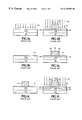
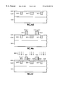
- FIGS. 1 a through 1 f are sequential depictions of a PRIOR ART MOSFET fabrication process showing typical Vt adjusts.
- FIGS. 2 a through 2 c are sequential depictions of a PRIOR ART MOSFET fabrication process showing multiple Vt adjust implant steps to achieve dual Vt performance capability.
- FIGS. 3 a through 3 c are sequential depictions of a PRIOR ART MOSFET fabrication process showing dual thickness oxide formation steps to achieve dual Vt performance capability.
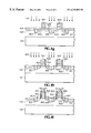
- FIGS. 4 a through 4 i depict a MOSFET fabrication process in accordance with the present invention.
- the foundational material for integrated circuit fabrication consists of a commercial silicon substrate 101 , doped with a relatively high p-type ion concentration, P+ (10 18 /cm 3 ).
- An epitaxial layer 103 consists of silicon having a lighter doping p-type ion concentration, P ⁇ (10 16 /cm 3 ).
- trenches 203 , 205 , 207 , 209 et seq. are formed in the epitaxial layer 103 . It will be recognized by a person skilled in the art that only a small segment of the surface of one integrated circuit dice, or “chip,” being fabricated on a silicon wafer in order to demonstrate the formation in accordance with the present invention of two, adjacent, exemplary MOSFETs having differing Vt characteristics. Multiple devices are simultaneously formed.
- the trenches 203 , 205 , 207 , 209 et seq. are filled with oxide 303 , 305 , 307 , 309 et seq., respectively, by a known manner technique.
- the filled trenches will provide p-type device/n-type device oxide regions known in the art as “shallow trench isolation” (“STI”) regions.
- STI shallow trench isolation
- LOCS Local oxidation of silicon
- FOX device field oxide
- isolation regions isolation regions, and the like processes are also compatible with the present invention.
- the silicon nitride mask 201 is stripped and the surface is planarized via a known manner wafer polishing process.
- the next step, as shown in FIG. 4 d is the formation of the gate oxide layer 401 , grown in accordance with known techniques, to form a layer having a thickness in the range of 1.5 to 2.5 nm.
- FIG. 4 e depicts the next step, the formation of polysilicon, or amorphous silicon, gate pillars 501 , 503 .
- LDC laterally doped channel
- An exemplary process parameter is a dopant implant energy of approximately 10-20 KeV for boron or 45-90 KeV for BF 2 at a concentration of about 1.0 to 2.5 ⁇ 10 13 ions/cm 2 using a zero tilt implant angle.
- FIG. 4 g represents the use of known manner implant oxidation at about 800 to 900 degrees C., to migrate the LDC regions 603 . This is followed by an implant, represented by arrows 701 , of lightly-doped source/drain (“LDD”) regions 703
- LDD lightly-doped source/drain
- the longer channel device on the right side of the FIGURE has no overlap in the LDC regions 603 . Therefore, the longer channel device has a higher leakage current, I OFF .
- the effect is inversely related to the chosen LDC energy. That is, use of a lower LDC energy increases the effect; with a higher LDC energy the effect is less, but device turn-on current, I ON , will be much higher.
- the process proceeds with known manner steps of forming gate sidewall spacers 800 , to serve as insulating films for subsequently formed electrodes.
- the spacers have a width in the range of approximately 50-to-100 nm.
- highly-doped source/drain implantation represented by arrows 801 , is performed—such as with arsenic at about 10-to-30 KeV and a concentration of approximately 2.0-to-4.0 ⁇ 10 15 ions/cm 2 , or with phosphorus at a like concentration at about 5-to-15 KeV—forming source/drain region 803 .
- Implants are then annealed—such as by using a rapid thermal annealing (“RTA”) process at about 1020-to-1050° C. for approximately 10-to-30 seconds—to activate the implanted regions as would be known in the art.
- RTA rapid thermal annealing
- gate electrodes 901 and source/drain electrodes 903 are formed using known manner salicidation process steps.
- the fully-formed gate pillars 501 , 503 are also referred to in the art as the “gate stack.”
- Having two gate lengths, namely Lg 1 and Lg 2 , in accordance with this process provides devices having different threshold voltages, Vt. Note that similarly, more than two gate lengths, Lg n , can be formed, resulting in devices of three or more threshold voltages, without multiple Vt adjust implants or formation of different thickness gate oxide layers being required.
Landscapes
- Engineering & Computer Science (AREA)
- Microelectronics & Electronic Packaging (AREA)
- Power Engineering (AREA)
- Physics & Mathematics (AREA)
- Condensed Matter Physics & Semiconductors (AREA)
- General Physics & Mathematics (AREA)
- Computer Hardware Design (AREA)
- Manufacturing & Machinery (AREA)
- Ceramic Engineering (AREA)
- Insulated Gate Type Field-Effect Transistor (AREA)
Abstract
An integrated circuit process technology for simultaneously forming multiple threshold voltage devices is disclosed. Devices having both high speed and low power consumption can be fabricated for use in integrated circuits having a need for both, such as microprocessors having cache memory.
Description
1. Field of the Invention
The present invention relates generally to integrated circuits and their fabrication processes. More specifically, the present invention relates to an integrated circuit fabrication process for making multi-threshold-voltage,“Vt,” integrated circuits and the devices fabricated with the process.
2. Description of Related Art
A common integrated circuit transistor device is the Metal Oxide Semiconductor Field Effect Transistor, or “MOSFET.” A typical MOSFET structure includes a pair of source/drain regions implanted into a surface of a silicon substrate, a gate oxide thin film formed on the substrate between the source/drain regions, and a gate electrode structure formed on the surface of the gate oxide. The region of the substrate itself between the source/drain regions is known as the channel region. The length of the channel region, “Lc,” is the distance between the source/drain regions. Typically, the channel length is less than the gate length, “Lg,” measured in the same dimension.
The threshold voltage, Vt, for a MOSFET device is defined as the applied gate-to-source voltage, “Vgs,” below which the MOSFET device drain-to-source current, “Ids,” becomes effectively zero (although a drain-to-source leakage current may still be present, it is considered negligible). The threshold voltage, Vt, is a function of a number of parameters, including gate material, gate insulation material and thickness, channel doping levels, impurity levels, source-to-substrate voltage, and the like as would be known to a person skilled in the art.
A prior art process is shown in FIGS. 1a-1 f. FIG. 1a depicts a silicon substrate material 10 that has a first conductivity type (e.g., for NMOS, having boron or BF2 impurities; for PMOS having arsenic or phosphorous impurities, at a first concentration level). A threshold adjust implant, represented by arrows 12, forms a substrate surface layer 10 a having a higher, second concentration of first conductivity type impurities. Typically, the impurity doping is at an injection energy of about 5-to-15 KeV at a concentration of about 8×10¹² ions/cm2. As shown in FIG. 1b, a gate oxide 14 is grown on the substrate surface region 10 a. Next, as illustrated by FIG. 1c, a gate electrode 16 structure, comprising a pillar of polysilicon is deposited on the gate oxide 14 and etched. Thereafter, as shown in FIG. 1d, lightly-doped source/drain (“LDD”) regions 18 are implanted with second conductivity type impurities, represented by arrows 19, at self-aligning positions with respect to the gate electrode 16 structure. For an exemplary NMOS device, arsenic ions are typically implanted at a concentration range of about 1×10¹⁴ to 1×10¹⁵ ions/cm2 at about 5 KeV. Looking to FIG. 1e, sidewall spacers 20, serving as insulating films, are formed by deposition and etching to each side of the gate electrode 16 pillar. Finally, as depicted in FIG. 1f, higher-doped source/drain regions 22 are implanted, represented by arrows 23, self-aligning to the spacers 20 between the LDD regions 18 and the Vt adjust implant surface layer 10 a. For the exemplary NMOS device, arsenic ions are implanted at a concentration of about 2×10¹⁵ ions/cm2 at about 5-to-10 KeV injection energy.
There is considerable technology developed for the manipulation of threshold voltage, Vt, referred to in the art as “Vt adjusts.” See e.g.: A Novel Source-to-Drain Nonuniformly Doped Channel MOSFET for High Current Drivability and Threshold Voltage Controllability, Okamura et al., IDEM 90, pp. 391-394; or, U.S. Pat. No. 5,466,957, Yuki et al.; or, assignee's own U.S. patent application Ser. No. 08/949,959, Milec-Strakalj & Yeap, for A MOS Device with Self-Compensating Vt-Implants, and assignee's own U.S. patent application Ser. No. 08/914,986, Krivokapic, for a Self-Aligned Channel Transistor and Method for Making Same.
In certain types of integrated circuit devices, for example microprocessors having a cache memory, there is a need for transistors performing both high speed logic and low power consumption which is generally measured by the OFF-state leakage current (a function of gate length). The same transistor can not achieve both; a shorter gate length will inherently have a higher leakage current. One solution has been the use of semiconductor device structures having two different Vt adjust implants. This is a relatively costly process. As shown in FIGS. 2a-2 c, it requires multiple Vt adjust implant steps to form devices with different Vt characteristics.
Another solution is the use of the use of two different gate oxide thicknesses. See e.g., A 0.18 um CMOS Logic Technology with Dual Gate Oxide and Low-k Interconnect for High-Performance and Low-Power Applications, Diaz et al., VLSI Technology Symposium 1999 report, proposing the support of 1.5-to-2 volt core logic as well as 3.3 volt periphery circuitry (input/output). As shown in FIGS. 3a-3 c, it requires multiple etch steps. This is a relatively complex and more costly process.
Another solution is provided in accordance with the present invention.
In its basic aspects, the present invention provides an integrated circuit fabrication process for making multi-threshold voltage (Vt,) circuit devices. The process includes the steps of: forming a gate oxide layer on a semiconductor substrate; forming a plurality of gate pillars having a plurality of gate length dimensions, Lgn, on the gate oxide layer such that a respective plurality of subjacent channel regions having corresponding channel lengths, Lcn, are formed in the substrate subjacent the gate pillars; and forming dopant implant regions in each of the subjacent channel regions and on first and second sides of the channel regions at each of the plurality of gate pillars respectively such that each combination of a dopant implant region, a channel region and a superjacent gate pillar thereof forms a semiconductor device having a characteristic threshold voltage, Vt, determined by a respective channel length thereof.
In another basic aspect, the present invention provides a method for fabrication of an integrated circuits such that each single integrated circuit has MOSFET devices having differing threshold voltage characteristics, including the steps of: providing a semiconductor substrate having an epitaxial layer; forming device isolation regions in the epitaxial layer; forming a gate oxide layer on the epitaxial layer; forming a plurality of MOSFET devices by forming a plurality of gate pillars on the gate oxide layer, wherein each of the gate pillars has a characteristic gate length dimension, Lgn, such that a respective plurality of subjacent channel regions having corresponding channel lengths, Lcn, are formed in the substrate subjacent the gate pillars, and wherein n≧2, and forming dopant implant regions in the subjacent channel regions and on first and second sides of the channel regions at each of the plurality of gate pillars respectively such that each combination of a source/drain region, a channel region and superjacent gate pillar thereof forms a semiconductor device having a threshold voltage, Vtn, determined by the respective channel length therein.
In another basic aspect, the present invention provides an integrated circuit having a plurality of MOSFET devices, each of the MOSFET devices having a characteristic threshold voltage (Vt). The circuit includes: a semiconductor substrate; at least one of a first MOSFET device having a first gate stack including a first gate oxide layer on the semiconductor substrate, a polysilicon or amorphous silicon first gate pillar, having a first gate length dimension, Lg1, and a first gate electrode atop the first gate pillar, and a respective first channel region subjacent the first gate stack having a first channel length, Lc1, in the substrate subjacent the first gate stack, and first dopant implant regions in the first channel region and on first and second sides of the first channel region respectively forming a first MOSFET device having a threshold voltage, Vt1, determined by the respective first channel length therein; and at least one of a second MOSFET device having a second gate stack including a second gate oxide layer on the semiconductor substrate, a polysilicon or amorphous silicon second gate pillar, having a second gate length dimension, Lg2, where Lg2 is greater than Lg1, and a second gate electrode atop the second gate pillar, and a respective second channel region subjacent the second gate stack having a second channel length, Lc1, where Lc2 is greater than Lc1, in the substrate subjacent the second gate stack, and second dopant implant regions in the second channel region and on first and second sides of the second channel region respectively forming a second MOSFET device having a threshold voltage, Vt2, determined by the respective second channel length therein, wherein the first MOSFET device is a high speed MOSFET device and the second MOSFET device is a low power consumption MOSFET device.
It is an advantage of the present invention that it reduces power consumption (OFF-state leakage).
It is an advantage of the present invention that it reduces the size of silicon area required for cache memory.
It is another advantage of the present invention that the simplification of process results in a better die yield.
Other objects, features and advantages of the present invention will become apparent upon consideration of the following explanation and the accompanying drawings, in which like reference designations represent like features throughout the drawings.
FIGS. 1a through 1 f are sequential depictions of a PRIOR ART MOSFET fabrication process showing typical Vt adjusts.
FIGS. 2a through 2 c are sequential depictions of a PRIOR ART MOSFET fabrication process showing multiple Vt adjust implant steps to achieve dual Vt performance capability.
FIGS. 3a through 3 c are sequential depictions of a PRIOR ART MOSFET fabrication process showing dual thickness oxide formation steps to achieve dual Vt performance capability.
FIGS. 4a through 4 i depict a MOSFET fabrication process in accordance with the present invention.
The drawings referred to in this specification should be understood as not being drawn to scale except if specifically noted.
Reference is made now in detail to a specific embodiment of the present invention, which illustrates the best mode presently contemplated by the inventors for practicing the invention. Alternative embodiments are also briefly described as applicable. It should be recognized that many publications describe the details of common techniques used in the fabrication process of integrated circuit components. See, e.g., Wolf, S., Silicon Processing for the VLSI Era, copyright 1990, Lattice Press; Sze, S. M., VLSI Technology, copyright 1988, McGraw-Hill; Ghandhi, S. K., VLSI Fabrication Principles, copyright 1983, John Wiley & Sons; or Semiconductor & Integrated Circuit Fabrication Techniques, Reston Publishing Co., Inc., copyright 1979 by the Fairchild Corporation. Those known manner techniques are generally employed in the fabrication of the structure of the present invention except in the steps required to accomplish the goals of the present invention; as such, an in depth description of known manner steps is unnecessary to an understanding of the present invention. Moreover, the individual steps of such a process can be performed using commercially available integrated circuit fabrication machines. See, e.g., Chapman, B., Glow Discharge Processes/Sputtering and Plasma Etching, copyright 1980, John Wiley & Sons. As specifically helpful to an understanding of the present invention, approximate technical data are set forth based upon current technology. Future developments in this art may call for appropriate adjustments as would be obvious to one skilled in the art.
It will be intuitively obvious to a person skilled in the art that the invention taught herein will have wide to applicability to integrated circuit fabrication processes; this description relies on an exemplary implementation of industrial applicability and no limitation on the scope of the invention is intended nor should any be implied therefrom.
It has been found that no Vt adjust implant nor formation of different thickness gate oxide layers is required in the formation of MOSFET devices to achieve the goal of faster device and smaller leakage current in integrated circuits incorporating multiple Vt devices.
Turning to FIG. 4a, the foundational material for integrated circuit fabrication consists of a commercial silicon substrate 101, doped with a relatively high p-type ion concentration, P+ (1018/cm3). An epitaxial layer 103 consists of silicon having a lighter doping p-type ion concentration, P− (1016/cm3).
As depicted in FIG. 4b, using a silicon nitride mask 201, trenches 203, 205, 207, 209 et seq., are formed in the epitaxial layer 103. It will be recognized by a person skilled in the art that only a small segment of the surface of one integrated circuit dice, or “chip,” being fabricated on a silicon wafer in order to demonstrate the formation in accordance with the present invention of two, adjacent, exemplary MOSFETs having differing Vt characteristics. Multiple devices are simultaneously formed.
As shown in FIG. 4c, the trenches 203, 205, 207, 209 et seq., are filled with oxide 303, 305, 307, 309 et seq., respectively, by a known manner technique. The filled trenches will provide p-type device/n-type device oxide regions known in the art as “shallow trench isolation” (“STI”) regions. [See, e.g., U.S. Pat. Nos. 5,759.871 (Hause et al.) and 5,767,000 (Fulford, Jr. et al.) assigned to the common assignee of the to present, incorporated herein by reference. Local oxidation of silicon, known as the “LOCOS,” to form device field oxide, “FOX,” isolation regions, and the like processes are also compatible with the present invention.] The silicon nitride mask 201 is stripped and the surface is planarized via a known manner wafer polishing process.
The next step, as shown in FIG. 4d is the formation of the gate oxide layer 401, grown in accordance with known techniques, to form a layer having a thickness in the range of 1.5 to 2.5 nm.
FIG. 4e depicts the next step, the formation of polysilicon, or amorphous silicon, gate pillars 501, 503. While using known fabrication processes, such as conventional photolithographic and trim plasma etching, note that different sizes are intentionally formed. For example, gate pillar 501 is etched to a gate length, “Lg1,” of 90 nm, while gate pillar 502 is etched to Lg2=150 nm.
Having gotten to this stage of fabrication without having to add any process steps in order to create dual Vt devices, the structure is ready for impurity implants in order to form dual Vt MOSFET devices. As illustrated in FIG. 4f, using the gate pillars 501, 503 as a self-aligned implant mask, laterally doped channel (“LDC”) implant forming regions 603 is made, such as with boron or BF2 as represented by arrows 601. An exemplary process parameter is a dopant implant energy of approximately 10-20 KeV for boron or 45-90 KeV for BF2 at a concentration of about 1.0 to 2.5×10¹³ ions/cm2 using a zero tilt implant angle.
FIG. 4g represents the use of known manner implant oxidation at about 800 to 900 degrees C., to migrate the LDC regions 603. This is followed by an implant, represented by arrows 701, of lightly-doped source/drain (“LDD”) regions 703 The LDD implant is made in the exemplary embodiment with arsenic ions at a concentration of about 5×10¹³ to 1.5×10¹⁵ ions/cm2 at 1-to-5 KeV.
Starting with FIG. 4g, another clear difference between short channel and long channel devices becomes apparent. The longer channel device on the right side of the FIGURE has no overlap in the LDC regions 603. Therefore, the longer channel device has a higher leakage current, IOFF. The effect is inversely related to the chosen LDC energy. That is, use of a lower LDC energy increases the effect; with a higher LDC energy the effect is less, but device turn-on current, ION, will be much higher.
Turning to FIG. 4h, the process proceeds with known manner steps of forming gate sidewall spacers 800, to serve as insulating films for subsequently formed electrodes. In the current exemplary embodiment, the spacers have a width in the range of approximately 50-to-100 nm. Next, highly-doped source/drain implantation, represented by arrows 801, is performed—such as with arsenic at about 10-to-30 KeV and a concentration of approximately 2.0-to-4.0×10¹⁵ ions/cm2, or with phosphorus at a like concentration at about 5-to-15 KeV—forming source/drain region 803.
Implants are then annealed—such as by using a rapid thermal annealing (“RTA”) process at about 1020-to-1050° C. for approximately 10-to-30 seconds—to activate the implanted regions as would be known in the art.
Finally, as shown in FIG. 4i, gate electrodes 901 and source/drain electrodes 903 are formed using known manner salicidation process steps. The fully-formed gate pillars 501, 503 are also referred to in the art as the “gate stack.”
Having two gate lengths, namely Lg1 and Lg2, in accordance with this process provides devices having different threshold voltages, Vt. Note that similarly, more than two gate lengths, Lgn, can be formed, resulting in devices of three or more threshold voltages, without multiple Vt adjust implants or formation of different thickness gate oxide layers being required.
The foregoing description of the preferred embodiment of the present invention has been presented for purposes of illustration and description. It is not intended to be exhaustive or to limit the invention to the precise form or to exemplary embodiments disclosed. Obviously, many modifications and variations will be apparent to practitioners skilled in this art. Similarly, any process steps described might be interchangeable with other steps in order to achieve the same result. The embodiment was chosen and described in order to best explain the principles of the invention and its best mode practical application, thereby to enable others skilled in the art to understand the invention for various embodiments and with various modifications as are suited to the particular use or implementation contemplated. It is intended that the scope of the invention be defined by the claims appended hereto and their equivalents.
Claims (13)
1. An integrated circuit fabrication process for making multi-threshold voltage (Vtn) circuit devices, the process comprising:
forming a gate oxide layer on a semiconductor substrate;
forming a plurality of gate pillars intentionally having a plurality of gate length dimensions, Lgn, on said gate oxide layer such that a respective plurality of subjacent channel regions having corresponding channel lengths, Lcn, are formed in said substrate subjacent said gate pillars; and
using said gate pillars as a self-aligned mask, forming dopant implant regions in each of said subjacent channel regions and on first and second sides of the channel regions at each of the plurality of gate pillars respectively such that each combination of a dopant implant region, a channel region and a superjacent gate pillar thereof forms a semiconductor device having a characteristic threshold voltage, Vt, determined by a respective channel length thereof, including adjusting LDC (laterally doped channel) dopant implant energy such that LDC regions are formed wherein the dopant implant energy controls leakage current and turn-on current relationship forming relatively short channel length devices having a high threshold voltage.
2. The integrated circuit fabrication process as set forth in claim 1, said step of forming dopant implant regions further comprising the step of:
using said gate pillars as a self-aligned mask, performing an LDC implant at a boron dopant implant energy in a range of approximately 10-20 KeV or a BF2 dopant implant energy in a range of approximately 45-90 KeV at a concentration in a range of about 1.0 to 2.5×10¹³ ions/cm2 using a zero tilt implant angle, wherein an LDC region is formed on said first and second sides of the channel regions.
3. The integrated circuit fabrication process as set forth in claim 2, said step of an LDC implant forming dopant implant regions further comprising the step of:
migrating said LCD region into said substrate and through said channel region by an implant oxidation at a temperature in a range of about 800 to 900 degrees C.
4. The integrated circuit fabrication process as set forth in claim 2, said step of forming dopant implant regions further comprising the step of:
following said step of performing an LDC implant, performing an LDD implant at a concentration of in a range of about 5×10¹³ to 1.5×10¹⁵ ions/cm2 at an implant energy having a range of about 1-to-5 KeV.
5. The integrated circuit fabrication process as set forth in claim 4, said step of forming dopant implant regions further comprising the step of:
following said step of performing an LDD implant, performing a highly-doped source/drain implantation of arsenic dopant on said first and second side in said substrate at an implant energy having a range of about 10-to-30 KeV and a concentration in a range of approximately 2.0-to-4.0×10¹⁵ ions/cm2.
6. The integrated circuit fabrication process as set forth in claim 4, said step of forming dopant implant regions further comprising the step of:
following said step of performing an LDD implant, performing a highly-doped source/drain implantation of phosphorus dopant at a concentration in the range of approximately 2.0-to-4.0×10¹⁵ ions/cm2 at an implant energy in a range of about 5-to-15 KeV, forming source/drain regions on said first and second side in said substrate.
7. A method for fabrication of an integrated circuits such that each single integrated circuit has MOSFET devices having differing threshold voltage characteristics, the method comprising:
providing a semiconductor substrate having an epitaxial layer;
forming device isolation regions in said epitaxial layer;
forming a gate oxide layer on the epitaxial layer;
forming a plurality of MOSFET devices by
forming a plurality of gate pillars on said gate oxide layer, wherein each of the gate pillars has a characteristic gate length dimension, Lgn, such that a respective plurality of subjacent channel regions having corresponding channel lengths, Lcn, are formed in said substrate subjacent said gate pillars, and wherein n is intentionally greater than or equal to 2, and
forming dopant implant regions in said subjacent channel regions and on first and second sides of the channel regions at each of the plurality of gate pillars respectively such that each combination of a source/drain region, a channel region and superjacent gate pillar thereof forms a semiconductor device having a threshold voltage, Vtn, determined by the respective channel length therein, including adjusting LDC (laterally doped channel) dopant implant energy such that LDC regions are formed wherein the dopant implant energy controls leakage current and turn-on current relationship forming relatively short channel length devices having a high threshold voltage such that shorter channel lengths than achieved in known manner lightly doped channel processes are provided.
8. The integrated circuit fabrication process as set forth in claim 7, said step of forming dopant implant regions further comprising the step of:
using said gate pillars as a self-aligned mask, performing an LDC implant at a boron dopant implant energy in a range of approximately 10-20 KeV or a BF2 dopant implant energy in a range of approximately 45-90 KeV at a concentration in a range of about 1.0 to 2.5×10¹³ ions/cm2 using a zero tilt implant angle, wherein an LDC region is formed on said first and second sides of the channel regions.
9. The integrated circuit fabrication process as set forth in claim 8, said step of an LDC implant forming dopant implant regions further comprising the step of:
migrating said LCD region into said substrate and through said channel region by an implant oxidation at a temperature in a range of about 800 to 900 degrees C.
10. The integrated circuit fabrication process as set forth in claim 9, said step of forming dopant implant regions further comprising the step of:
following said step of performing an LDC implant, performing an LDD implant at a concentration of in a range of about 5×10¹³ to 1.5×10¹⁵ ions/cm2 at an implant energy having a range of about 1-to-5 KeV.
11. The integrated circuit fabrication process as set forth in claim 10, said step of forming dopant implant regions further comprising the step of:
following said step of performing an LDD implant, performing a highly-doped source/drain implantation of phosphorus dopant at a concentration in the range of approximately 2.0-to-4.0×10¹⁵ ions/cm2 at an implant energy in a range of about 5-to-15 KeV, forming source/drain regions on said first and second side in said substrate.
12. The integrated circuit fabrication process as set forth in claim 10, said step of forming dopant implant regions further comprising the step of:
following said step of performing an LDD implant, performing a highly-doped source/drain implantation of arsenic dopant on said first and second side in said substrate at an implant energy having a range of about 10-to-30 KeV and a concentration in a range of approximately 2.0-to-4.0×10¹⁵ ions/cm2.
13. An integrated circuit having a plurality of MOSFET devices, each of said MOSFET devices having a characteristic threshold voltage (Vt), said circuit comprising:
a semiconductor substrate;
at least one of a first MOSFET device having a first gate stack including a first gate oxide layer on the semiconductor substrate, a polysilicon or amorphous silicon first gate pillar, having a first gate length dimension, Lg1, and a first gate electrode atop said first gate pillar, and a respective first channel region subjacent said first gate stack having a first channel length, Lc1, in said substrate subjacent said first gate stack, and first dopant implant regions in the first channel region and on first and second sides of the first channel region respectively forming a first MOSFET device having a threshold voltage, Vt1, determined by the respective first channel length therein; and
at least one of a second MOSFET device having a second gate stack including a second gate oxide layer on the semiconductor substrate, a polysilicon or amorphous silicon second gate pillar, having a second gate length dimension, Lg2, where Lg2 is greater than Lg1, and a second gate electrode atop said second gate pillar, and a respective second channel region subjacent said second gate stack having a second channel length, Lc1, where Lc2 is greater than Lc1, in said substrate subjacent said second gate stack, and second dopant implant regions in the second channel region and on first and second sides of the second channel region respectively forming a second MOSFET device having a threshold voltage, Vt2, determined by the respective second channel length therein, wherein said first MOSFET device is a high speed MOSFET device and said second MOSFET device is a low power consumption MOSFET device wherein said channel length LC2 is less than a channel length achieved in known manner lightly doped channel processes.
Priority Applications (1)
| Application Number | Priority Date | Filing Date | Title |
|---|---|---|---|
| US09/289,909 US6238982B1 (en) | 1999-04-13 | 1999-04-13 | Multiple threshold voltage semiconductor device fabrication technology |
Applications Claiming Priority (1)
| Application Number | Priority Date | Filing Date | Title |
|---|---|---|---|
| US09/289,909 US6238982B1 (en) | 1999-04-13 | 1999-04-13 | Multiple threshold voltage semiconductor device fabrication technology |
Publications (1)
| Publication Number | Publication Date |
|---|---|
| US6238982B1 true US6238982B1 (en) | 2001-05-29 |
Family
ID=23113681
Family Applications (1)
| Application Number | Title | Priority Date | Filing Date |
|---|---|---|---|
| US09/289,909 Expired - Lifetime US6238982B1 (en) | 1999-04-13 | 1999-04-13 | Multiple threshold voltage semiconductor device fabrication technology |
Country Status (1)
| Country | Link |
|---|---|
| US (1) | US6238982B1 (en) |
Cited By (24)
| Publication number | Priority date | Publication date | Assignee | Title |
|---|---|---|---|---|
| US6365466B1 (en) * | 2001-01-31 | 2002-04-02 | Advanced Micro Devices, Inc. | Dual gate process using self-assembled molecular layer |
| US6420767B1 (en) * | 2000-06-28 | 2002-07-16 | Advanced Micro Devices, Inc. | Capacitively coupled DTMOS on SOI |
| US6426534B1 (en) * | 2000-05-01 | 2002-07-30 | Xilinx, Inc. | Methods and circuits employing threshold voltages for mask-alignment detection |
| US6468852B1 (en) | 2001-08-03 | 2002-10-22 | Micron Technology, Inc. | Methods of forming field effect transistors; methods of forming DRAM circuitry |
| US6534399B1 (en) | 2001-01-24 | 2003-03-18 | Advanced Micro Devices, Inc. | Dual damascene process using self-assembled monolayer |
| US6630404B1 (en) | 2001-03-14 | 2003-10-07 | Advanced Micro Devices, Inc. | Reducing feature dimension using self-assembled monolayer |
| US6703304B1 (en) | 2001-01-30 | 2004-03-09 | Advanced Micro Devices, Inc. | Dual damascene process using self-assembled monolayer and spacers |
| US20040080016A1 (en) * | 2002-08-30 | 2004-04-29 | Houston Theodore W. | Integrated circuit cells |
| US20040094804A1 (en) * | 2002-11-20 | 2004-05-20 | International Business Machines Corporation | Method and process to make multiple-threshold metal gates CMOS technology |
| US20040102026A1 (en) * | 2002-11-26 | 2004-05-27 | Nga-Ching Wong | Lateral doped channel |
| US20040185093A1 (en) * | 2003-03-18 | 2004-09-23 | Szymczak Christopher E. | Compositions containing sucralose |
| US20040232498A1 (en) * | 2001-01-23 | 2004-11-25 | Fuji Electric Co., Ltd. | Semiconductor integrated circuit device and manufacture method therefore |
| US6849492B2 (en) | 2002-07-08 | 2005-02-01 | Micron Technology, Inc. | Method for forming standard voltage threshold and low voltage threshold MOSFET devices |
| US20060189061A1 (en) * | 2004-02-25 | 2006-08-24 | Amos Ricky S | CMOS silicide metal gate integration |
| US20100155854A1 (en) * | 2008-12-22 | 2010-06-24 | Knut Stahrenberg | Methods of Fabricating Semiconductor Devices and Structures Thereof |
| US20110175169A1 (en) * | 2010-01-15 | 2011-07-21 | International Business Machines Corporation | Cmos circuit with low-k spacer and stress liner |
| US8298895B1 (en) * | 2011-10-31 | 2012-10-30 | International Business Machines Corporation | Selective threshold voltage implants for long channel devices |
| US8629016B1 (en) | 2011-07-26 | 2014-01-14 | Suvolta, Inc. | Multiple transistor types formed in a common epitaxial layer by differential out-diffusion from a doped underlayer |
| US8642415B2 (en) | 2012-05-03 | 2014-02-04 | International Business Machines Corporation | Semiconductor substrate with transistors having different threshold voltages |
| US20150104919A1 (en) * | 2013-08-19 | 2015-04-16 | SK Hynix Inc. | Three-dimensional semiconductor device, variable resistive memory device including the same, and method of manufacturing the same |
| US9070477B1 (en) | 2012-12-12 | 2015-06-30 | Mie Fujitsu Semiconductor Limited | Bit interleaved low voltage static random access memory (SRAM) and related methods |
| US9348402B2 (en) | 2013-02-19 | 2016-05-24 | Qualcomm Incorporated | Multiple critical paths having different threshold voltages in a single processor core |
| US9391076B1 (en) | 2011-08-23 | 2016-07-12 | Mie Fujitsu Semiconductor Limited | CMOS structures and processes based on selective thinning |
| US20170040322A1 (en) * | 2015-08-05 | 2017-02-09 | Samsung Electronics Co., Ltd. | Semiconductor devices and methods of manufacturing the same |
Citations (10)
| Publication number | Priority date | Publication date | Assignee | Title |
|---|---|---|---|---|
| US4963501A (en) * | 1989-09-25 | 1990-10-16 | Rockwell International Corporation | Method of fabricating semiconductor devices with sub-micron linewidths |
| US5273926A (en) * | 1991-06-27 | 1993-12-28 | Texas Instruments Incorporated | Method of making flash EEPROM or merged FAMOS cell without alignment sensitivity |
| US5629548A (en) * | 1994-02-12 | 1997-05-13 | Kabushiki Kaisha Toshiba | Semiconductor device with adjustable channel width |
| US5795803A (en) * | 1996-08-29 | 1998-08-18 | Sharp Kabushiki Kaisha | Method for manufacturing a semiconductor device |
| US5847432A (en) * | 1995-01-11 | 1998-12-08 | Mitsubishi Denki Kabushiki Kaisha | Semiconductor device and production method therefor |
| US5858827A (en) * | 1994-09-29 | 1999-01-12 | Sony Corporation | Method of manufacturing MOS transistor device with improved threshold value control and reduced reverse short channel effect |
| US5895954A (en) * | 1997-03-27 | 1999-04-20 | Mitsubishi Denki Kabushiki Kaisha | Field effect transistor with impurity concentration peak under gate electrode |
| US5970331A (en) * | 1998-01-07 | 1999-10-19 | Advanced Micro Devices, Inc. | Method of making a plug transistor |
| US5990516A (en) * | 1994-09-13 | 1999-11-23 | Kabushiki Kaisha Toshiba | MOSFET with a thin gate insulating film |
| US6077736A (en) * | 1996-06-10 | 2000-06-20 | Lg Semicon Co., Ltd. | Method of fabricating a semiconductor device |
-
1999
- 1999-04-13 US US09/289,909 patent/US6238982B1/en not_active Expired - Lifetime
Patent Citations (10)
| Publication number | Priority date | Publication date | Assignee | Title |
|---|---|---|---|---|
| US4963501A (en) * | 1989-09-25 | 1990-10-16 | Rockwell International Corporation | Method of fabricating semiconductor devices with sub-micron linewidths |
| US5273926A (en) * | 1991-06-27 | 1993-12-28 | Texas Instruments Incorporated | Method of making flash EEPROM or merged FAMOS cell without alignment sensitivity |
| US5629548A (en) * | 1994-02-12 | 1997-05-13 | Kabushiki Kaisha Toshiba | Semiconductor device with adjustable channel width |
| US5990516A (en) * | 1994-09-13 | 1999-11-23 | Kabushiki Kaisha Toshiba | MOSFET with a thin gate insulating film |
| US5858827A (en) * | 1994-09-29 | 1999-01-12 | Sony Corporation | Method of manufacturing MOS transistor device with improved threshold value control and reduced reverse short channel effect |
| US5847432A (en) * | 1995-01-11 | 1998-12-08 | Mitsubishi Denki Kabushiki Kaisha | Semiconductor device and production method therefor |
| US6077736A (en) * | 1996-06-10 | 2000-06-20 | Lg Semicon Co., Ltd. | Method of fabricating a semiconductor device |
| US5795803A (en) * | 1996-08-29 | 1998-08-18 | Sharp Kabushiki Kaisha | Method for manufacturing a semiconductor device |
| US5895954A (en) * | 1997-03-27 | 1999-04-20 | Mitsubishi Denki Kabushiki Kaisha | Field effect transistor with impurity concentration peak under gate electrode |
| US5970331A (en) * | 1998-01-07 | 1999-10-19 | Advanced Micro Devices, Inc. | Method of making a plug transistor |
Non-Patent Citations (2)
| Title |
|---|
| C.H. Diaz et al., A 0.18um CMOS Logic Technology with Dual Gate Oxide and . . . , TSMC, Taiwan ROC, VLSI Tech. Symposium 1999. |
| Matsuki et al., "Laterally-Doped Channel (LDC) Structure for Sub-Quarter Micron MOSFETs", VLSI Technology, 1991. Digest of Technical Papers Symposium, pp. 113-114, May 28-30, 1991.* |
Cited By (61)
| Publication number | Priority date | Publication date | Assignee | Title |
|---|---|---|---|---|
| US6426534B1 (en) * | 2000-05-01 | 2002-07-30 | Xilinx, Inc. | Methods and circuits employing threshold voltages for mask-alignment detection |
| US6465305B1 (en) * | 2000-05-01 | 2002-10-15 | Xilinx, Inc. | Methods and circuits employing threshold voltages for mask-alignment detection |
| US6420767B1 (en) * | 2000-06-28 | 2002-07-16 | Advanced Micro Devices, Inc. | Capacitively coupled DTMOS on SOI |
| US20040232498A1 (en) * | 2001-01-23 | 2004-11-25 | Fuji Electric Co., Ltd. | Semiconductor integrated circuit device and manufacture method therefore |
| US7138311B2 (en) | 2001-01-23 | 2006-11-21 | Fuji Electric Co., Ltd. | Semiconductor integrated circuit device and manufacture method therefore |
| US6833594B2 (en) * | 2001-01-23 | 2004-12-21 | Fuji Electric Co., Ltd. | Semiconductor integrated circuit device and manufacture method therefore |
| US6534399B1 (en) | 2001-01-24 | 2003-03-18 | Advanced Micro Devices, Inc. | Dual damascene process using self-assembled monolayer |
| US6703304B1 (en) | 2001-01-30 | 2004-03-09 | Advanced Micro Devices, Inc. | Dual damascene process using self-assembled monolayer and spacers |
| US6365466B1 (en) * | 2001-01-31 | 2002-04-02 | Advanced Micro Devices, Inc. | Dual gate process using self-assembled molecular layer |
| US6630404B1 (en) | 2001-03-14 | 2003-10-07 | Advanced Micro Devices, Inc. | Reducing feature dimension using self-assembled monolayer |
| US6468852B1 (en) | 2001-08-03 | 2002-10-22 | Micron Technology, Inc. | Methods of forming field effect transistors; methods of forming DRAM circuitry |
| US7413946B2 (en) | 2002-07-08 | 2008-08-19 | Micron Technology, Inc. | Formation of standard voltage threshold and low voltage threshold MOSFET devices |
| US7189607B2 (en) | 2002-07-08 | 2007-03-13 | Micron Technology, Inc. | Formation of standard voltage threshold and low voltage threshold MOSFET devices |
| US20110006372A1 (en) * | 2002-07-08 | 2011-01-13 | Round Rock Research, Llc | Formation of standard voltage threshold and low voltage threshold mosfet devices |
| US7755146B2 (en) | 2002-07-08 | 2010-07-13 | Round Rock Research, Llc | Formation of standard voltage threshold and low voltage threshold MOSFET devices |
| US7696579B2 (en) | 2002-07-08 | 2010-04-13 | Micron Technology, Inc. | Formation of standard voltage threshold and low voltage threshold MOSFET devices |
| US20090286366A1 (en) * | 2002-07-08 | 2009-11-19 | Micron Technology, Inc. | Formation of standard voltage threshold and low voltage threshold mosfet devices |
| US6849492B2 (en) | 2002-07-08 | 2005-02-01 | Micron Technology, Inc. | Method for forming standard voltage threshold and low voltage threshold MOSFET devices |
| US20050026352A1 (en) * | 2002-07-08 | 2005-02-03 | Mark Helm | Formation of standard voltage threshold and low voltge threshold MOSFET devices |
| US20050227427A1 (en) * | 2002-07-08 | 2005-10-13 | Mark Helm | Formation of standard voltage threshold and low voltage threshold MOSFET devices |
| US20060003513A1 (en) * | 2002-07-08 | 2006-01-05 | Mark Helm | Formation of standard voltage threshold and low voltage threshold MOSFET devices |
| US7439140B2 (en) | 2002-07-08 | 2008-10-21 | Micron Technology, Inc. | Formation of standard voltage threshold and low voltage threshold MOSFET devices |
| US20080042216A1 (en) * | 2002-07-08 | 2008-02-21 | Mark Helm | Formation of standard voltage threshold and low voltage threshold mosfet devices |
| US7304353B2 (en) | 2002-07-08 | 2007-12-04 | Micron Technology, Inc. | Formation of standard voltage threshold and low voltage threshold MOSFET devices |
| US7265012B2 (en) | 2002-07-08 | 2007-09-04 | Micron Technology, Inc. | Formation of standard voltage threshold and low voltage threshold MOSFET devices |
| US8053321B2 (en) | 2002-07-08 | 2011-11-08 | Round Rock Research, Llc | Formation of standard voltage threshold and low voltage threshold MOSFET devices |
| US6996787B2 (en) * | 2002-08-30 | 2006-02-07 | Texas Instruments Incorporated | Integrated circuit cells |
| US6734521B2 (en) * | 2002-08-30 | 2004-05-11 | Texas Instruments Incorporated | Integrated circuit cells |
| US20040080016A1 (en) * | 2002-08-30 | 2004-04-29 | Houston Theodore W. | Integrated circuit cells |
| US20040094804A1 (en) * | 2002-11-20 | 2004-05-20 | International Business Machines Corporation | Method and process to make multiple-threshold metal gates CMOS technology |
| CN1294648C (en) * | 2002-11-20 | 2007-01-10 | 国际商业机器公司 | Method and process to make multiple-threshold value |
| US6846734B2 (en) | 2002-11-20 | 2005-01-25 | International Business Machines Corporation | Method and process to make multiple-threshold metal gates CMOS technology |
| US7049188B2 (en) | 2002-11-26 | 2006-05-23 | Advanced Micro Devices, Inc. | Lateral doped channel |
| CN100414708C (en) * | 2002-11-26 | 2008-08-27 | 斯班逊有限公司 | Method of producing a laterally doped channel |
| WO2004049446A1 (en) * | 2002-11-26 | 2004-06-10 | Advanced Micro Devices, Inc. | Method of producing a laterally doped channel |
| US20040102026A1 (en) * | 2002-11-26 | 2004-05-27 | Nga-Ching Wong | Lateral doped channel |
| KR101037775B1 (en) * | 2002-11-26 | 2011-05-27 | 어드밴스드 마이크로 디바이시즈, 인코포레이티드 | Method of producing a laterally doped channel |
| US20040185093A1 (en) * | 2003-03-18 | 2004-09-23 | Szymczak Christopher E. | Compositions containing sucralose |
| US7411227B2 (en) * | 2004-02-25 | 2008-08-12 | International Business Machines Corporation | CMOS silicide metal gate integration |
| US20060189061A1 (en) * | 2004-02-25 | 2006-08-24 | Amos Ricky S | CMOS silicide metal gate integration |
| US20100155854A1 (en) * | 2008-12-22 | 2010-06-24 | Knut Stahrenberg | Methods of Fabricating Semiconductor Devices and Structures Thereof |
| US9087919B2 (en) | 2008-12-22 | 2015-07-21 | Infineon Technologies Ag | Methods of fabricating semiconductor devices and structures thereof |
| US8252649B2 (en) | 2008-12-22 | 2012-08-28 | Infineon Technologies Ag | Methods of fabricating semiconductor devices and structures thereof |
| US9659778B2 (en) | 2008-12-22 | 2017-05-23 | Infineon Technologies Ag | Methods of fabricating semiconductor devices and structures thereof |
| US8432014B2 (en) | 2008-12-22 | 2013-04-30 | Infineon Technologies Ag | Methods of fabricating semiconductor devices and structures thereof |
| US8778765B2 (en) | 2008-12-22 | 2014-07-15 | Infineon Technologies Ag | Methods of fabricating semiconductor devices and structures thereof |
| US8222100B2 (en) * | 2010-01-15 | 2012-07-17 | International Business Machines Corporation | CMOS circuit with low-k spacer and stress liner |
| US20110175169A1 (en) * | 2010-01-15 | 2011-07-21 | International Business Machines Corporation | Cmos circuit with low-k spacer and stress liner |
| US8629016B1 (en) | 2011-07-26 | 2014-01-14 | Suvolta, Inc. | Multiple transistor types formed in a common epitaxial layer by differential out-diffusion from a doped underlayer |
| US8653604B1 (en) | 2011-07-26 | 2014-02-18 | Suvolta, Inc. | Multiple transistor types formed in a common epitaxial layer by differential out-diffusion from a doped underlayer |
| US8916937B1 (en) | 2011-07-26 | 2014-12-23 | Suvolta, Inc. | Multiple transistor types formed in a common epitaxial layer by differential out-diffusion from a doped underlayer |
| US9391076B1 (en) | 2011-08-23 | 2016-07-12 | Mie Fujitsu Semiconductor Limited | CMOS structures and processes based on selective thinning |
| US8298895B1 (en) * | 2011-10-31 | 2012-10-30 | International Business Machines Corporation | Selective threshold voltage implants for long channel devices |
| US8642415B2 (en) | 2012-05-03 | 2014-02-04 | International Business Machines Corporation | Semiconductor substrate with transistors having different threshold voltages |
| US9070477B1 (en) | 2012-12-12 | 2015-06-30 | Mie Fujitsu Semiconductor Limited | Bit interleaved low voltage static random access memory (SRAM) and related methods |
| US9348402B2 (en) | 2013-02-19 | 2016-05-24 | Qualcomm Incorporated | Multiple critical paths having different threshold voltages in a single processor core |
| US20150104919A1 (en) * | 2013-08-19 | 2015-04-16 | SK Hynix Inc. | Three-dimensional semiconductor device, variable resistive memory device including the same, and method of manufacturing the same |
| US9318576B2 (en) * | 2013-08-19 | 2016-04-19 | SK Hynix Inc. | Method of manufacturing three-dimensional semiconductor device and variable resistive memory device |
| US20170040322A1 (en) * | 2015-08-05 | 2017-02-09 | Samsung Electronics Co., Ltd. | Semiconductor devices and methods of manufacturing the same |
| KR20170017123A (en) * | 2015-08-05 | 2017-02-15 | 삼성전자주식회사 | Semiconductor device and method for fabricating the same |
| US9825033B2 (en) * | 2015-08-05 | 2017-11-21 | Samsung Electronics Co., Ltd. | Semiconductor devices and methods of manufacturing the same |
Similar Documents
| Publication | Publication Date | Title |
|---|---|---|
| US6238982B1 (en) | Multiple threshold voltage semiconductor device fabrication technology | |
| US6255152B1 (en) | Method of fabricating CMOS using Si-B layer to form source/drain extension junction | |
| US7470593B2 (en) | Method for manufacturing a cell transistor of a semiconductor memory device | |
| US5841170A (en) | Field effect transistor and CMOS element having dopant exponentially graded in channel | |
| US6255154B1 (en) | Semiconductor device and method of manufacturing the same | |
| US9768074B2 (en) | Transistor structure and fabrication methods with an epitaxial layer over multiple halo implants | |
| US8076228B2 (en) | Low noise transistor and method of making same | |
| US5903029A (en) | Insulated-gate field-effect transistor and method for producing the same | |
| JP2701762B2 (en) | Semiconductor device and manufacturing method thereof | |
| US7009258B2 (en) | Method of building a CMOS structure on thin SOI with source/drain electrodes formed by in situ doped selective amorphous silicon | |
| US6391728B1 (en) | Method of forming a highly localized halo profile to prevent punch-through | |
| US6051459A (en) | Method of making N-channel and P-channel IGFETs using selective doping and activation for the N-channel gate | |
| JP2001156290A (en) | Semiconductor device | |
| US6162694A (en) | Method of forming a metal gate electrode using replaced polysilicon structure | |
| US6268256B1 (en) | Method for reducing short channel effect | |
| US6350656B1 (en) | SEG combined with tilt side implant process | |
| US20020068410A1 (en) | Method of manufacturing low-leakage, high-performance device | |
| KR100556350B1 (en) | Semiconductor device and fabricating Method for the same | |
| US6630386B1 (en) | CMOS manufacturing process with self-amorphized source/drain junctions and extensions | |
| US20080160710A1 (en) | Method of fabricating mosfet device | |
| US11488871B2 (en) | Transistor structure with multiple halo implants having epitaxial layer over semiconductor-on-insulator substrate | |
| US8048730B2 (en) | Semiconductor device and method for manufacturing the same | |
| KR20010061597A (en) | Transistor and method for manufacturing the same | |
| US7101746B2 (en) | Method to lower work function of gate electrode through Ge implantation | |
| KR940006672B1 (en) | Fabricating method of mos transistor |
Legal Events
| Date | Code | Title | Description |
|---|---|---|---|
| AS | Assignment |
Owner name: ADVANCED MICRO DEVICES, CALIFORNIA Free format text: ASSIGNMENT OF ASSIGNORS INTEREST;ASSIGNORS:KRIVOKAPIC, ZORAN;MILIC, OGNJEN;REEL/FRAME:009892/0342 Effective date: 19990409 |
|
| STCF | Information on status: patent grant |
Free format text: PATENTED CASE |
|
| FEPP | Fee payment procedure |
Free format text: PAYOR NUMBER ASSIGNED (ORIGINAL EVENT CODE: ASPN); ENTITY STATUS OF PATENT OWNER: LARGE ENTITY |
|
| FPAY | Fee payment |
Year of fee payment: 4 |
|
| FPAY | Fee payment |
Year of fee payment: 8 |
|
| FPAY | Fee payment |
Year of fee payment: 12 |