US6285617B1 - Semiconductor memory device preventing malfunction during refresh operation even when noise is superimposed on control signal - Google Patents
Semiconductor memory device preventing malfunction during refresh operation even when noise is superimposed on control signal Download PDFInfo
- Publication number
- US6285617B1 US6285617B1 US09/556,775 US55677500A US6285617B1 US 6285617 B1 US6285617 B1 US 6285617B1 US 55677500 A US55677500 A US 55677500A US 6285617 B1 US6285617 B1 US 6285617B1
- Authority
- US
- United States
- Prior art keywords
- signal
- control signal
- activation
- row
- refresh
- Prior art date
- Legal status (The legal status is an assumption and is not a legal conclusion. Google has not performed a legal analysis and makes no representation as to the accuracy of the status listed.)
- Expired - Fee Related
Links
Images


Classifications
-
- G—PHYSICS
- G11—INFORMATION STORAGE
- G11C—STATIC STORES
- G11C11/00—Digital stores characterised by the use of particular electric or magnetic storage elements; Storage elements therefor
- G11C11/21—Digital stores characterised by the use of particular electric or magnetic storage elements; Storage elements therefor using electric elements
- G11C11/34—Digital stores characterised by the use of particular electric or magnetic storage elements; Storage elements therefor using electric elements using semiconductor devices
- G11C11/40—Digital stores characterised by the use of particular electric or magnetic storage elements; Storage elements therefor using electric elements using semiconductor devices using transistors
- G11C11/401—Digital stores characterised by the use of particular electric or magnetic storage elements; Storage elements therefor using electric elements using semiconductor devices using transistors forming cells needing refreshing or charge regeneration, i.e. dynamic cells
- G11C11/406—Management or control of the refreshing or charge-regeneration cycles
- G11C11/40611—External triggering or timing of internal or partially internal refresh operations, e.g. auto-refresh or CAS-before-RAS triggered refresh
-
- G—PHYSICS
- G11—INFORMATION STORAGE
- G11C—STATIC STORES
- G11C11/00—Digital stores characterised by the use of particular electric or magnetic storage elements; Storage elements therefor
- G11C11/21—Digital stores characterised by the use of particular electric or magnetic storage elements; Storage elements therefor using electric elements
- G11C11/34—Digital stores characterised by the use of particular electric or magnetic storage elements; Storage elements therefor using electric elements using semiconductor devices
- G11C11/40—Digital stores characterised by the use of particular electric or magnetic storage elements; Storage elements therefor using electric elements using semiconductor devices using transistors
- G11C11/401—Digital stores characterised by the use of particular electric or magnetic storage elements; Storage elements therefor using electric elements using semiconductor devices using transistors forming cells needing refreshing or charge regeneration, i.e. dynamic cells
- G11C11/406—Management or control of the refreshing or charge-regeneration cycles
- G11C11/40618—Refresh operations over multiple banks or interleaving
-
- G—PHYSICS
- G11—INFORMATION STORAGE
- G11C—STATIC STORES
- G11C11/00—Digital stores characterised by the use of particular electric or magnetic storage elements; Storage elements therefor
- G11C11/21—Digital stores characterised by the use of particular electric or magnetic storage elements; Storage elements therefor using electric elements
- G11C11/34—Digital stores characterised by the use of particular electric or magnetic storage elements; Storage elements therefor using electric elements using semiconductor devices
- G11C11/40—Digital stores characterised by the use of particular electric or magnetic storage elements; Storage elements therefor using electric elements using semiconductor devices using transistors
- G11C11/401—Digital stores characterised by the use of particular electric or magnetic storage elements; Storage elements therefor using electric elements using semiconductor devices using transistors forming cells needing refreshing or charge regeneration, i.e. dynamic cells
- G11C11/4063—Auxiliary circuits, e.g. for addressing, decoding, driving, writing, sensing or timing
- G11C11/407—Auxiliary circuits, e.g. for addressing, decoding, driving, writing, sensing or timing for memory cells of the field-effect type
- G11C11/408—Address circuits
- G11C11/4085—Word line control circuits, e.g. word line drivers, - boosters, - pull-up, - pull-down, - precharge
Definitions
- the present invention relates to semiconductor memory devices and, more specifically to a semiconductor memory device performing a CBR (CAS before RAS) refresh operation.
- CBR CAS before RAS
- DRAM Dynamic Random Access Memory
- a refresh operation must periodically be performed to prevent disruption of the stored information by a leakage current.
- word lines provided correspondingly to rows of the memory cells are sequentially selected, and accumulated electric charges are read for all memory cells on the selected word lines and rewritten after amplification.
- a voltage at a storage node in the memory cell is reset at an initial value even if it has been reduced by the leakage current.
- a maximum value of a refresh interval assuring prevention of data disruption for every memory cell is trefmx and the number of word lines is N.
- a relationship of tcrf ⁇ trefmx/N must be held to enable a refresh operation with a given refresh cycle tcrf corresponding to an interval between word lines in order to prevent disruption of stored information by a leakage current. Accordingly, if the number of word lines increases due to an increase in a storage capacity of memories, the refresh cycle must correspondingly be reduced.
- a refresh cycle is ensured by increasing the number of word lines simultaneously selected during a refresh operation as compared with that during a normal reading/writing operation in order to increase the number of rows subjected to a single refresh operation.
- a refresh operation performed during a random access operation such as a reading/writing operation
- a refresh operation performed only for retaining stored information in a chip as performed during a battery backup period Especially in the former refresh operation, a CBR (CAS before RAS) refresh has been widely used in terms of saving the number of terminals.
- the start of the refresh operation is instructed by reversing the order of activating a row address strobe signal /RAS and a column address strobe signal /CAS, which are inherently control signals, with respect to the order during a normal reading/writing operation without providing a control signal dedicated to the refresh operation.
- FIG. 14 is a schematic diagram showing a memory array 500 of a DRAM structured to select a greater number of word lines during the refresh operation than during a normal operation.
- memory array 500 has a plurality of memory cells arranged in a matrix.
- memory array 500 is of a 64-Mbit size addressed by address bits A 0 to A 12 of an address signal of 13 bits.
- Memory array 500 is divided into two regions 500 a and 500 b of the same size in a row direction. In each of regions 500 a and 500 b , word lines are provided correspondingly to rows of the memory cells.
- the last bit A 12 of the address signal is used for selecting one of regions 500 a and 500 b of the memory array.
- regions 500 a and 500 b one memory cell row is selected and a corresponding word line is activated in accordance with a combination of the remaining address bits A 0 to A 11 of 12 bits.
- the word lines corresponding to the same combination of signal levels of address bits A 0 to A 11 are provided in both of regions 500 a and 500 b.
- FIG. 14 representatively shows word lines WLa and WLb correspondingly designated by address bits A 0 to A 11 in regions 500 a and 500 b .
- Word drivers WDa and WDb are respectively provided for word lines WLa and WLb.
- Word driver WDa receives a block selection signal RAD 12 set correspondingly to address bit A 12 , a word line activation signal RXT, and an address decode signal ADC activated in accordance with a combination of address bits A 0 to A 11 for driving word line WLa into a selection state when all of these signals are activated.
- a word driver is arranged which activates the corresponding word line in accordance with signals as in the case of word driver WDa.
- word line driver WDb receives a block selection signal ZRAD 12 which is complementary to block selection signal RAD 12 in accordance with address bit A 12 as well as word line activation signal RXT and address decode signal ADC also applied to word driver WDa for operation.
- one of block selection signals RAD 12 and ZRAD 12 is activated (H level) in response to a signal level of address bit A 12 , and a word line corresponding to address bits A 0 to A 11 is activated in one of regions 500 a and 500 b .
- both of block selection signals ZRAD 12 and RAD 12 are activated (H level) regardless of the signal level of address bit A 12 .
- corresponding word lines are activated in regions 500 a and 500 b in accordance with a combination of address bits A 0 to A 11 . Accordingly, in memory array 500 , twice as many word lines are simultaneously activated during the refresh operation as compared with the case of the normal operation. Such a structure ensures a refresh cycle for the memory cell array with a large storage capacity.
- FIG. 15 is a timing chart shown in conjunction with a row related operation during a normal operation of memory array 500 .
- /RAS is a row address strobe signal designating activation of a row related operation.
- /CAS is a column address strobe signal designating activation of a column related operation.
- a 12 represents a signal level of address bit A 12 , and control signals RASF and CAS are respectively inverted signals of row address strobe signal /RAS and column address strobe signal /CAS, obtained as outputs from a control signal.
- a signal ZRASE is an inverted signal of control signal RASF
- a control signal RADE is a row address decode enable signal activated when a prescribed period of time is elapsed after activation of row address strobe signal /RAS in response to the start of the row related operation.
- Control signals RXT and S 0 N are respectively a word line activation signal and a sense amplifier activation signal. Activation timings for signals RXT and S 0 N are controlled such that the word line and the sense amplifier are suitably timed to be activated in response to the start of the row related operation.
- a refresh control signal ZCBR is inactivated (H level) during the normal operation and activated (L level) for designating a refresh operation for CBR refresh.
- refresh control signal ZCBR when refresh control signal ZCBR is activated, both of block selection signals ZRAD 12 and RAD 12 are activated (H level).
- refresh control signal ZCBR is inactivated (H level)
- one of block selection signals ZRAD 12 and RAD 12 is activated (H level) in accordance with the signal level of address bit A 12 .
- control signals RASF and ZRASE are sequentially activated (level) and row address decode enable signal RADE, word line activation signal RXT and sense amplifier activation signal S 0 N are activated.
- Block selection signal ZRAD 12 corresponding to the signal level (L level) of address A 12 is activated (H level) in response to activation of row address decode enable signal RADE, and RAD 12 is maintained in an inactivation state (L level).
- the column related operation starts in response to activation of column address strobe signal /CAS at a time t 1 , and a data reading/writing operation is performed on memory cells in region 500 b selected by the address signal.
- FIG. 16 is a circuit diagram showing a structure of a conventional refresh control circuit 510 generating a refresh control signal ZCBR.
- refresh control circuit 510 includes an SR flip flop 512 receiving two inputs of control signals CAS and RASF, and an SR flip flop 514 receiving two inputs of control signal RASF and control signal ZRF which is an output from SR flip flop 512 .
- SR flip flop 514 outputs a refresh control signal ZCBR.
- FIG. 17A shows states of control signal ZRF in relation to a combination of control signals RASF and CAS, corresponding to a truth table of SR flip flop 512 .
- FIG. 17B shows states of refresh control signal ZCBR in relation to a combination of control signals ZRF and RASF, corresponding to a truth table of SR flip flop 514 .
- FIG. 18 is a timing chart shown in conjunction with a row related operation for CBR refresh in memory array 500 .
- column address strobe signal /CAS is activated prior to activation of row address strobe signal /RAS (time t 0 ). This corresponds to the state in which control signal CAS is risen to the H level when control signal RASF is at the L level, so that control signal ZRF is correspondingly set at the L level.
- control signal RASF changes from the L to H level in response to activation of row address strobe signal /RAS (time t 1 )
- refresh control signal ZCBR is activated (L level) while control signal ZRF is maintained at the L level.
- block selection signal ZRAD 12 is activated (H level) in addition to block selection signal ZRAD 12 activated in response to the signal level of address bit A 12 .
- control signals RXD and S 0 N are sequentially activated, so that corresponding word lines and sense amplifiers are also sequentially activated.
- a refresh operation can be performed on the corresponding word lines.
- the CBR refresh operation once started, completes when control signal ZRF is brought back into the inactivation state (H level) in response to inactivation of row address strobe signal /CAS after control signal ZRF is inactivated (H level) in response to inactivation of column address strobe signal /CAS.
- control signal ZRF and a refresh control signal ZCBR are maintained in the inactivation state (H level), so that the normal reading/writing operation is performed.
- refresh control circuit 510 In the structure of refresh control circuit 510 shown in FIG. 16, 5 however, if noise is superimposed on row address strobe signal /RAS when both of row address strobe signal /RAS and column address strobe signal /CAS are activated (L level) during the normal operation, erroneous activation of the refresh control signal may be caused, resulting in disruption of data in the memory cell. This will now be described in detail.
- both of control signal ZRF and refresh control signal ZCBR are at the H level at t 2 at which the noise is caused.
- the level of control signal ZRF responsively changes from H to L level.
- control signal RASF also returns back to the H level from the L level.
- refresh control signal ZCBR is activated (L level).
- block selection signal RAD 12 is newly activated in addition to block selection signal ZRAD 12 which has been activated in response to the signal level of address bit A 12 .
- the word line in region 500 a which is not essentially subjected to activation, is activated.
- region 500 a which is not essentially subjected to activation, if the word line is activated when the sense amplifier is not activated, the sense amplifier may be activated at an incorrect timing before electric charges corresponding to stored information and accumulated in the memory cells connected to the word line are sufficiently transmitted to the bit line, thereby disrupting data in the memory cell.
- the word line is activated in the state in which the sense amplifier for region 500 a is activated, the data in the memory cell connected to the word line may be disrupted as electric charges from the memory cells are not amplified by the sense amplifier.
- FIGS. 19A and 19B are timing charts shown in conjunction with activation timings of the word line and sense amplifier as well as data reading.
- FIGS. 19A and 19B show an operation of reading retained data to the bit line by activation of the bit line and sense amplifier for the memory cell in which data at the H level is retained.
- V WL represents a voltage level of the word line
- control signal S 0 N represents an activation signal for the sense amplifier
- V BL represents a voltage level of the bit line.
- FIG. 19A shows a correct activation timing at which the word line is activated prior to activation of the sense amplifier.
- bit line voltage V BL is set at a precharge potential Vpc before a time ta at which the word line is activated.
- bit line voltage V BL is changed to reflect the H level of data retained in the memory cell.
- the sense amplifier operates to amplify a potential difference between a complementary pair of bit lines in response to activation of sense amplifier activation signal S 0 N at a time tb, so that bit line voltage V BL is amplified to attain to the H level. Because of an appropriate time lag between ta and tb, even if the level of the bit line voltage gradually changes toward the direction opposite to the voltage level of the data retained in the memory cell immediately after the word line is driven, the sense amplifier is activated after the voltage level corresponding to the retained data appears as a bit line voltage. Thus, the voltage level of the data retained in the memory cell can correctly be amplified by the sense amplifier.
- bit line voltage V BL is changed to attain to the H or L level after a time tc at which the amplifier has already been activated.
- the word line is selected at a time td so that electric charges move from the memory cell in response to the increase in word line voltage V WL , data of the memory cell is disadvantageously disrupted and lost due to a large driving current of the sense amplifier.
- An object of the present invention is to provide a semiconductor memory device capable of preventing malfunction during a refresh operation even if pulse-like noise is superimposed on a control signal.
- the present invention is a semiconductor memory device starting a refresh operation in accordance with an activation order of first and second control signals, and includes a control circuit, a memory cell array, and a row selection circuit.
- the control circuit generates an internal control signal activated/inactivated respectively in accordance with activation/inactivation of the second control signal, and designates start and end of the refresh operation in accordance with the first and second control signals as well as the internal control signal.
- the memory cell array has a plurality of memory cells arranged in a matrix and is divided into a plurality of row blocks in a direction of rows of the memory cells. Each of the plurality of row blocks has a plurality of word lines arranged correspondingly to a plurality of memory cell rows.
- the row selection circuit selects one of the memory cell rows in each of the plurality of row blocks in accordance with an address signal.
- the row selection circuit is controlled by the control circuit for activating one of the plurality of word lines corresponding to the selected memory cell row in at least one of the plurality of row blocks during a normal reading/writing operation, and activating one of the plurality of word lines corresponding to the selected memory cell row in each of the greater number of row blocks during a refresh operation than during the normal reading/writing operation.
- a main advantage of the present invention is that the start and end of the refresh operation is designated in accordance with a signal level of the internal control signal in addition to a combination of signal levels of the first and second control signals essentially required for designating a precharge operation, so that a refresh cycle can be ensured while preventing disruption of data in the memory cell even when noise is superimposed on the control signal.
- FIG. 1 is a block diagram showing an overall structure of a semiconductor memory device 1000 according to the first embodiment of the present invention.
- FIG. 2 is a block diagram shown in conjunction with a structure of a memory cell array 40 .
- FIG. 3 is a circuit am showing an exemplary structure of a refresh control circuit 110 .
- FIGS. 4A and 4B are diagrams shown in conjunction with a relationship among control signals in refresh control circuit 110 .
- FIG. 5 is a timing chart shown in conjunction with an operation of refresh circuit 110 when noise is superimposed on a signal /RAS.
- FIG. 6 is a circuit diagram showing an exemplary structure of a row related operation control circuit 120 .
- FIG. 7 is a circuit diagram showing an exemplary structure of an internal address generating circuit 151 .
- FIG. 8 is a diagram shown in conjunction with a logic gate 156 outputting a control signal ZQAL.
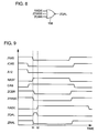
- FIG. 9 is a timing chart shown in conjunction with states of control signals during a CBR refresh operation.
- FIG. 10 is a circuit diagram showing an exemplary structure of a block select signal generating circuit 152 .
- FIG. 11 is a circuit diagram showing an exemplary structure of a refresh control circuit 210 according to the first modification of the first embodiment.
- FIG. 12 is a circuit diagram showing an exemplary structure of a refresh control circuit 310 according to the second modification of the first embodiment.
- FIG. 13 is a circuit diagram showing an exemplary structure of a refresh control circuit 410 according to the third modification of the first embodiment.
- FIG. 14 is a schematic diagram showing a memory array 500 of a DRAM structured to select the greater number of word lines during a refresh operation than during a normal operation.
- FIG. 15 is a timing chart shown in conjunction with a row related operation during a normal operation in memory array 500 .
- FIG. 16 is a circuit diagram showing a structure of a conventional refresh control circuit 510 .
- FIGS. 17A and 17B are diagrams shown in conjunction with a relationship among control signals in refresh control circuit 510 .
- FIG. 18 is a timing chart shown in conjunction with a row related operation during a CBR refresh operation in memory array 500 .
- FIGS. 19A and 19B are timing charts shown in conjunction with a relationship among activation timings of the word line and sense amplifier as well as data reading.
- semiconductor memory device 1000 is provided having a memory cell array 40 of 64-Mbits addressed by address signals of 13 bits. While a structure of memory cell array 40 will later be described in detail, here, assume that it is divided into two regions 40 a and 40 b as in the conventional case. Of address bits A 0 to A 12 of address signals, A 12 is an address signal for selecting one of regions 40 a and 40 b for row selection.
- semiconductor memory device 1000 includes: an address input terminal 10 receiving address bits A 0 to A 12 of the address signal; a control signal input terminal 12 receiving control signals such as a row address strobe signal /RAS, column address strobe signal /CAS, write enable signal /WE, output enable signal /OE and the like; an address buffer 20 provided correspondingly to address input terminal 10 ; and a control signal buffer 22 provided correspondingly to control signal input terminal 12 .
- Control signal buffer 22 outputs control signals RASF, CAS, WE and OE, which are inverted signals of the control signals input to control signal input terminal 12 .
- Semiconductor memory device 1000 further includes: a control circuit 30 receiving a control signal output from control signal buffer 22 for controlling the overall reading/writing operation and refresh operation of semiconductor memory device 1000 ; a memory cell array 40 having a plurality of memory cells arranged in a matrix; a row selection circuit 60 for selecting rows of the memory cell; and a column selection circuit 70 selecting columns of the memory cells.
- memory cell array 40 is divided into a plurality of row blocks 45 in a row direction. Assume that memory cell array 40 is divided into two regions 40 a and 40 b as in the conventional case. Thus, each of regions 40 a and 40 b has the same number of row blocks 45 .
- Each of row blocks 45 has a plurality of memory cells arranged in a matrix.
- a word line is arranged for every row of the memory cells, and a pair of bit lines BL and /BL (not shown) are arranged for every column of the memory cells.
- a sense I/O circuit 50 Arranged in a region adjacent to row block 45 in a column direction is a sense I/O circuit 50 which amplifies a voltage caused between the pair of bit lines in accordance with selection of the word lines and is controlled by column selection circuit 70 for transmitting the amplified data signal to an I/O line 85 .
- Each sense I/O circuit 50 has a so-called shared amplifier structure, being shared by two adjacent row blocks 45 .
- Sense I/O circuit 50 is activated by sense amplifier activation signal S 0 N output from control circuit 30 .
- Sense amplifier activation signal S 0 N is activated upon the start of the row related operation in response to activation of row address strobe signal /RAS. Activation of sense I/O circuit 50 can be performed for every pair of two regions 40 a , 40 b or for every row block 45 .
- Row selection circuit 60 includes: a decode circuit (not shown) decoding internal row address bits RAD ⁇ 0 > to RAD ⁇ 11 > which are bits of the internal row address signal output from address selection circuit 150 ; and word drivers for activating corresponding word lines in accordance with word line activation signal RXT output from control circuit 30 , block selection signals RAD 12 , ZRAD 12 output from address selection circuit 150 , and decode signal ADC output from the decode circuit.
- a decode circuit (not shown) decoding internal row address bits RAD ⁇ 0 > to RAD ⁇ 11 > which are bits of the internal row address signal output from address selection circuit 150 ; and word drivers for activating corresponding word lines in accordance with word line activation signal RXT output from control circuit 30 , block selection signals RAD 12 , ZRAD 12 output from address selection circuit 150 , and decode signal ADC output from the decode circuit.
- FIG. 2 representatively shows word lines WLa and WLb selected in respective regions in accordance with the same combination of internal row address bits RAD ⁇ 0 > to RAD ⁇ 11 >.
- a word driver WDa arranged correspondingly to word line WLa in region 40 a operates in response to word line activation signal RXT, address decode signal ADC and block selection signal RAD 12 for activating the word line selected by internal row address when block selection signal RAD 12 is in an active state (H level).
- a word driver WDb activates the word line selected by internal address signals RAD ⁇ 0 > to RAD ⁇ 11 > at a timing designated by control signal RXT when block selection signal ZRAD 12 is in the active state (H level).
- One of block selection signals RAD 12 and ZRAD 12 is activated (H level) in a complementary manner in accordance with a signal level of address bit A 12 during a normal reading/writing operation.
- both of block selection signals RAD 12 and ZRAD 12 are brought into the active state (H level).
- the word lines corresponding to internal address signals RAD ⁇ 0 > to RAD ⁇ 11 > are simultaneously activated.
- semiconductor memory device 1000 further includes: an input/output circuit 80 inputting/outputting data to/from sense I/O circuit 50 in memory cell array 40 through I/O line 85 ; and a data input/output terminal 90 inputting/outputting input/output data with respect to an external portion.
- Input/output circuit 80 is controlled by control circuit 30 for inputting/outputting data read/written with respect to memory cell array 40 to/from data input/output terminal 90 .
- Control circuit 30 receives control signals RASF, CAS, WE and OE output from a control signal buffer 22 for outputting an internal control signal for controlling an overall operation of semiconductor memory device 1000 .
- Control circuit 30 includes: a refresh control circuit 110 generating a refresh control signal ZCBR; row related operation control circuit 120 outputting row address decode enable signal RADE, word line activation signal RXT and sense amplifier activation signal S 0 N; and an internal refresh address counter 130 outputting address bits Q ⁇ 0 > to Q ⁇ 11 > of an internal refresh address for selecting a word line to be subjected to a refresh operation when the refresh operation is designated.
- Control circuit 30 further includes an address selection circuit 150 receiving address bits A ⁇ 0 > to A ⁇ 12 > and internal refresh address bits Q ⁇ 0 > to Q ⁇ 11 > for outputting internal row address bits RAD ⁇ 0 > to RAD ⁇ 11 > and block selection signals RAD 12 , ZRAD 12 for row selection as well as internal column address bits CAD ⁇ 0 > to CAD ⁇ 12 > for column selection.
- address selection circuit 150 receiving address bits A ⁇ 0 > to A ⁇ 12 > and internal refresh address bits Q ⁇ 0 > to Q ⁇ 11 > for outputting internal row address bits RAD ⁇ 0 > to RAD ⁇ 11 > and block selection signals RAD 12 , ZRAD 12 for row selection as well as internal column address bits CAD ⁇ 0 > to CAD ⁇ 12 > for column selection.
- address selection circuit 150 sets signal levels of internal row address bits RAD ⁇ 0 > to RAD ⁇ 11 > in accordance with signal levels of address bits A ⁇ 0 > to A ⁇ 11 > output from address buffer 20 and activates one of block selection signals RAD 12 and ZRAD 12 in accordance with a signal level of address bit A ⁇ 12 > during the normal operation.
- address selection circuit 150 sets signal levels of internal row address bits RAD ⁇ 0 > to RAD ⁇ 11 > in accordance with signal levels of internal refresh address bits Q ⁇ 0 >to Q ⁇ 11 > output from internal refresh address counter 130 and activates both of block selection signals RAD 12 and ZRAD 12 .
- address selection circuit 150 sets signal levels of internal column address bits CAD ⁇ 0 > to CAD ⁇ 12 > in accordance with signal levels of address bits A ⁇ 0 > to A ⁇ 12 > output from address buffer 20 .
- Column selection circuit 70 selects memory cell columns in response to internal column address bits CAD ⁇ 0 > to CAD ⁇ 12 >.
- the word line corresponding to a combination of internal row address bits RAD ⁇ 0 > to RAD ⁇ 11 > is activated in one of regions 40 a and 40 b in response to the block selection signal during the normal operation, and the word lines corresponding to internal row address bits RAD ⁇ 0 > to RAD ⁇ 11 > is activated in both of regions 40 a and 40 b during the refresh operation.
- Semiconductor memory device 1000 according to the first embodiment is characterized in that a structure of the refresh control circuit is different from that of the conventional case.
- FIG. 3 is a circuit diagram showing an exemplary structure of refresh control circuit 110 .
- refresh control circuit 110 includes: a logic gate 112 outputting an OR operation result of control signal RASF and row address decode enable signal RADE which is an internal control signal activated upon the start of the column related operation corresponding to activation of control signal RASF; an SR flip flop 114 receiving two inputs from control signal CAS and an output from logic gate 112 ; and an SR flip flop 116 receiving two inputs of a signal ZRF, an output from SR flip flop 112 , and a control signal RASF.
- SR flip flop 116 outputs refresh control signal ZCBR.
- Refresh control circuit 110 is different from conventional refresh control circuit 510 shown in FIG. 16 in that one of inputs to SR flip flop 114 is not directly used as control signal RASF, but the OR operation result of internal control signal RADE activated upon the start of the row related operation and control signal RASF is used
- FIG. 4A shows states of control signal ZRF with respect to a combination of control signals RASF, RADE and CAS, corresponding to a truth table of SR flip flop 114 .
- FIG. 4B shows states of refresh control signal ZCBR with respect to a combination of control signals ZRF and RASF, corresponding to a truth table of SR flip flop 116 .
- Refresh control circuit 110 performs activation (L level) of control signal ZRF necessary for activation of refresh control signal ZCBR only when both of control signals RASF and RADE are at the L level.
- L level activation of control signal ZRF necessary for activation of refresh control signal ZCBR only when both of control signals RASF and RADE are at the L level.
- RASF is activated (L level) prior to activation of column address strobe signal /CAS, so that the row related operation starts for a normal reading/writing operation. More specifically, in response to activation (H level) of control signal RASF, which is an inverted signal of row address strobe signal /RAS, row address decode enable signal RADE, word line activation signal RXT and sense amplifier S 0 N are sequentially activated.
- control signal RASF rises to the H level when control signal CAS is in an inactive state (L level), so that control signal ZRF is set at the H level.
- column address strobe signal /CAS is activated (L level) to activate the column related operation. Accordingly, the column selecting operation is performed, and data reading or writing is performed with respect to the memory cell corresponding to the selected memory cell column of a group of memory cells connected to the selected word line.
- refresh control circuit 110 Although control signal CAS rises to the H level, an output from logic gate 112 , the other input to SR flip flop 114 , is also at the H level, so that signal ZRF is maintained at the H level. Thus, refresh control signal ZCBR is also maintained in the inactive state (H level), and the refresh operation is not started.
- refresh control circuit 110 An operation of refresh control circuit 110 in this state is considered. While the detail will later be given, when the row related operation is once started by Tow address strobe signal /RAS, row address decode enable signal RADE is a signal generated to be maintained in the activation state until the row related operation ends. Accordingly, even when control signal RASF instantly changes to the L level in response to noise at a time t 2 , internal control signal RADE is maintained at the H level.
- control signal ZRF does not change from the H to L level due to instant noise caused to row address strobe signal /RAS and control signal ZRF is maintained at the H level.
- refresh control signal ZCBR which is in the inactive state (H level) before the noise is caused, is not activated (L level). Therefore, the problem is prevented which is associated with disruption of the data retained in the corresponding memory cell when the noise is caused to row address strobe signal /RAS, a refresh control signal is erroneously activated even during the normal reading/writing operation, and the word line is newly selected, as described with reference to FIG. 15 .
- control circuit 30 Next, exemplary structures of circuits included in control circuit 30 will be described in detail.
- FIG. 6 is a circuit diagram showing an exemplary structure of row related operation control circuit 120 .
- Row related operation control circuit 120 generates an internal control signal associated with the row related operation in response to control signal RASF activated in accordance with row address strobe signal /RAS.
- row related control circuit 120 includes: an inverter IV 10 inverting control signal RASF and outputting control signal ZRASE; a buffer 121 receiving control signal ZRASE for outputting control signal ZRAL for latching address bits A ⁇ 0 > to A ⁇ 11 >; an inverter IV 12 inverting and outputting control signal ZRAL; a buffer 122 delaying and outputting control signal S 0 N; and a logic gate 126 outputting an OR operation result receiving outputs from buffer 122 and inverter IV 12 as two inputs.
- Logic gate 126 outputs row address decode enable signal RADE for designating the start of decoding a row address.
- Row related operation control circuit 120 further includes: a buffer 124 delaying and outputting row address decode enable signal RADE; an inverter IV 14 inverting control signal ZRASE; a buffer 123 delaying an output from inverter IV 14 ; and a logic gate 128 outputting an AND operation result of outputs from buffers 123 and 124 .
- Logic gate 128 outputs word line activation signal RXT.
- Word line activation signal RXT is input to buffer 125 .
- Buffer 125 delays word line activation signal RXT for outputting sense amplifier activation signal S 0 N.
- row address decode enable signal RADE in response to control signal RAS set at the H level upon activation (L level) of row address strobe signal /RAS, row address decode enable signal RADE, word line activation signal RXT and sense amplifier activation signal S 0 N are sequentially activated (H level) after a delay time caused by the inverter and buffer.
- row address strobe signal /RAS when row address strobe signal /RAS is inactivated (H level), word line activation signal RXT and sense amplifier activation signal S 0 N are inactivated (L level) when a prescribed period of time caused by the inverter and buffer is elapsed in accordance with the change of control signal RASF to the L level.
- output from logic gate 126 In response to inactivation of sense amplifier activation signal S 0 N, output from logic gate 126 also changes to the L level. Responsively, row address decode enable signal RADE is also inactivated (L level).
- sense amplifier activation signal S 0 N is activated, even if a signal level of control signal RAS changes due to noise, taking an OR with respect to control signal S 0 N, which has already been changed to the H level by logic gate 126 , prevents row address decode enable signal RADE from changing to the L level until the end the sense operation.
- refresh control signal ZCBR is generated by using control signal RADE maintained in the active state during the row related operation while not being affected by noise superimposed on row address strobe signal /RAS. Accordingly, even when the noise is superimposed on row address strobe signal /RAS during the normal operation, if the noise corresponds to a short period of time within a prescribed delay time to the end of the sense amplifier operation, refresh control signal ZCBR is not disadvantageously activated.
- word line activation signal RXT and sense amplifier activation signal S 0 N the influence of a change in signal level of row address strobe signal /RAS does not appear until a prescribed delay time caused by the inverter and buffer is elapsed.
- the superimposed noise corresponds to a short period of time, the possibility that the noise affects at the same timing as row address strobe signal /RAS, word line activation signal RXT and sense amplifier activation signal S 0 N is low.
- row related operation control circuit 120 is not limited to that shown in FIG. 6 .
- An arbitrary circuit structure may be used as long as it can activate/inactivate the internal control signal associated with the row related operation at a prescribed timing shown in FIG. 5 .
- FIG. 7 is a circuit diagram showing an exemplary structure of an internal address generating circuit 151 generating internal row address bits RAD ⁇ 0 > to RAD ⁇ 11 > included in the address selection circuit.
- Internal address generating circuit 151 selectively latches one of a group of address bits A ⁇ 0 > to A ⁇ 11 > applied from address buffer 20 and a group of internal refresh address bits Q ⁇ 0 > to Q ⁇ 11 > applied from internal refresh address counter 130 for outputting them as internal row address bits RAD ⁇ 0 > to RAD ⁇ 11 >.
- FIG. 7 shows an exemplary structure of an internal address generating circuit corresponding to the nth address bit (n: an integer from 0 to 11).
- internal address generating circuit 151 includes: an inverter IV 20 inverting a signal level of address bit A ⁇ n> applied from address buffer 20 ; a transfer gate TG 10 connected between inverter IV 20 and node Na; and a docked inverter IV 28 inverting a signal level of an internal refresh address bit Q ⁇ n> applied from internal refresh address counter 130 .
- Transfer gate TG 10 is turned on/off in response to control signal ZRAL generated by row related operation control circuit 120 .
- Clocked inverter IV 28 is activated in response to control signal ZQAL.
- Internal address generating circuit 151 further includes: an inverter IV 22 inverting a signal level of node Na and outputting it to a node Nb; an inverter IV 26 provided to form a latch circuit with inverter IV 22 ; an inverter IV 24 inverting a signal level of node Nb; a logic gate 152 outputting an AND operation result of the signal level at node Nb and the signal level of row address decode enable signal RADE as internal row address bit RAD ⁇ n>; and a logic gate 154 outputting an AND operation result obtained by two inputs of row address decode enable signal RADE and an output signal from inverter IV 24 as an inverted signal ZRAD ⁇ n> of the internal row address bit.
- control signal ZQAL will be described.
- logic gate 156 outputs as a control signal ZQAL an NOR calculate result obtained by three inputs of row address decode enable signals RADE, a control signal ZRASE which is an inverted signal of control signal RASF, and a refresh control signal ZCBR.
- control signal ZQAL is activated (H level) and docked inverter IV 28 operates only when all of these three inputs are at the L level.
- row address strobe signal /RAS is activated (L level) at t 1 after column address strobe signal /CAS is activated (L level), so that the CBR refresh operation starts and refresh control signal ZCBR is activated (L level).
- control signal RASF changes to the H level in response to activation of row address strobe signal /RAS and control signal ZRASE changes to the L level, so that the row related operation starts.
- Row address decode enable signal RADE is maintained at the L level until t 2 when a prescribed period of time is elapsed after the row related operation is started, and activated (H level) at t 2 .
- control signal ZQAL is activated (H level) and internal refresh address bit Q ⁇ n> is transmitted to nodes Na and Nb and latched thereat.
- control signal ZRAL receives a signal level of an address bit input from an address input terminal through address buffer 20 and latches it at nodes Na and Nb prior to activation of row address strobe signal /RAS, i.e., before the row related operation is started.
- row selection circuit 60 receiving internal row address bits RAD ⁇ 0 > to RAD ⁇ 11 > performs row selection in response to the externally input address bit during the normal operation, and performs row selection in response to internal refresh address bits Q ⁇ 0 > to Q ⁇ 11 > transmitted from internal refresh address counter 130 during the refresh operation.
- FIG. 10 is a circuit diagram showing an exemplary structure of a block selection signal generating circuit 152 included in address selection circuit 150 .
- block selection signal generating circuit 152 includes: an inverter IV 30 inverting a signal level of address bit A ⁇ 12 > output from address buffer 20 in response to the last bit A 12 of the address signal used for selecting a block in row selection; a transfer gate TG 20 connected between inverter IV 30 and node Nc; an inverter IV 32 inverting a signal level of node Nc and outputting it to a node Nd; an inverter IV 36 arranged to form a latch circuit with inverter IV 32 ; and an inverter IV 34 inverting a signal level at node Nd.
- Transfer gate TG 20 is turned on when control signal ZRAL is at the H level, and turned off when the row related operation is started and control signal ZRAL changes to the L level.
- transfer gate TG 20 is turned on, the signal level of address bit A ⁇ 12 > output from address buffer 20 is latched at node Nd.
- Block selection signal generating circuit 152 further includes; an inverter IV 38 inverting and outputting a row address decode enable signal RADE; a logic gate 162 outputting an OR operation result obtained by two inputs of an inverted signal of an output from inverter IV 38 and an inverted signal of control signal ZRASE; and an SR flip flop 164 receiving two inputs of a refresh control signal ZCBR and an output from logic gate 162 .
- SR flip flop 164 outputs a control signal RADSEL 4 K.
- Control signal RADSEL 4 K is responsive to activation (L level) of refresh control signal ZCBR and set at the H level.
- Block selection signal generating circuit 152 further includes: a logic gate 166 outputting an OR operation result obtained by two inputs of a signal level at node Nd and control signal RADSEL 4 K; a logic gate 168 outputting an OR operation result obtained by two inputs of an output signal from inverter IV 34 and control signal RADSEL 4 K; a logic gate 170 outputting an AND operation result obtained by two inputs of an output from logic gate 166 and row address decode enable signal RADE; and a logic gate 172 outputting an AND operation result obtained by two inputs of an output from logic gate 168 and row address decode enable signal RADE.
- Logic gate 170 outputs a block selection signal RAD ⁇ 12 >
- logic gate 172 outputs a block selection signal ZRAD ⁇ 12 >.
- control signal RADSEL 4 K When control signal RADSEL 4 K is activated (H level) in response to activation (L level) of refresh control signal ZCBR, both outputs from logic gates 166 and 168 attain to the H level.
- block selection signals RAD ⁇ 12 > and ZRAD ⁇ 12 > are both activated regardless of the signal level of address bit A ⁇ 12 > at a timing at which row address decode enable signal RADE is activated (H level).
- RADSEL 4 K is set at the L level, so that outputs from logic gates 166 and 168 are respectively set at the signal level of address bit A ⁇ 12 > and an inverted level thereof. Accordingly, upon activation of row address decode enable signal RADE, one of block selection signals RAD ⁇ 12 > and ZRAD ⁇ 12 > is activated (H level) in accordance with the signal level of address bit A ⁇ 12 >.
- control signal RADSEL 4 K is responsively set at the H level.
- both of block selection signals RAD ⁇ 12 > and ZRAD ⁇ 12 > are activated even during the normal operation, thereby disrupting data retained in the memory cell.
- exemplary circuit structures of internal address generating circuit 151 and block selection signal generating circuit 152 are merely examples. Other circuit structures may be employed as long as they can change the selecting manner of internal row address bits RAD ⁇ 0 > to RAD ⁇ 11 > and block selection signals RAD 12 , ZRAD 12 as described above during the normal operation and the refresh operation.
- refresh control circuit 110 has the structure shown in FIG. 3 .
- refresh control signal ZCBR is not erroneously activated even if the noise is caused to row address strobe signal /RAS during the normal operation.
- block selection signal generating circuit 152 does not erroneously activate both block selection signals, and the problem associated with the conventional case is above avoided.
- the structure in which the memory cell array is divided into two portions and one of these regions is selected using the last bit of the address signal as a block selection signal.
- control of the block selection signal using at least one bit of the address signal is merely an example, and an independent control signal may be provided and externally input.
- the bit number of the control signal for block selection can be increased, so that the memory cell array is correspondingly divided into a greater number of portions.
- the start of the CBR refresh operation is controlled by using an existing internal control signal used for control of the row related operation, so that malfunction in the CBR refresh operation when the noise is caused to row address strobe signal /RAS is prevented.
- refresh control signal ZCBR is controlled by row address decode enable signal RADE which is an internal control signal associated with the row related operation, and malfunction in the CBR refresh operation is prevented.
- refresh control circuit 210 according to the first modification of the first embodiment is different from refresh control circuit 110 described with reference to FIG. 3 in that one of outputs from logic gate 112 is word line activation signal RXT instead of row address decode enable signal RADE.
- RXT word line activation signal
- RADE row address decode enable signal
- Word line activation signal RXT is activated/inactivated in response to activation/inactivation of row address strobe signal /RAS, respectively.
- the signal level of word line activation signal RXT corresponds row address strobe signal /RAS being delayed by the inverter and delay circuit.
- the noise affects word line activation signal RXT after a period during which the signal level of row address strobe signal /RAS changes. Accordingly, if the noise corresponds to a short period of time, an OR operation result of control signal RASF and word line activation signal RXT, i.e., a level of an output signal from logic gate 112 is maintained at the H level without being affected by the noise.
- word line activation signal RXT is used instead of row address decode enable signal RADE, an effect similar to that in the case of the first embodiment can be produced.
- refresh control circuit 310 according to the second modification of the first embodiment is different from refresh control circuit 110 shown in FIG. 3 in that one of outputs from logic gate 112 is used as a sense amplifier activation signal S 0 N instead of row address decode enable signal RADE.
- the other parts of the structure and operation of the circuit are the same as those of semiconductor memory device 1000 in accordance with the first embodiment and therefore description thereof will not be repeated.
- Sense amplifier activation signal S 0 N is activated/inactivated in responsive to activation/inactivation of row address strobe signal /RAS like word line activation signal RXT, respectively.
- a signal level of sense amplifier activation signal S 0 N corresponds to row address strobe signal /RAS delayed by the inverter and delay circuit.
- sense amplifier activation signal S 0 N can be used instead of row address decode enable signal RADE to produce an effect similar to that in the first embodiment.
- refresh circuit 410 according to the third modification of the first embodiment is different from refresh circuit 110 shown in FIG. 3 in that one of outputs from logic gate 112 is used as a delay signal of control signal RASF, which is an output from delay circuit 405 , instead of row address decode enable signal RADE.
- RASF delay signal of control signal
- RADE row address decode enable signal
- a delay signal of control signal RASF can be used in place of row address decode enable signal RADE to produce an effect similar to that in the first embodiment.
Abstract
Description
Claims (6)
Applications Claiming Priority (2)
| Application Number | Priority Date | Filing Date | Title |
|---|---|---|---|
| JP11-308767 | 1999-10-29 | ||
| JP30876799A JP2001126472A (en) | 1999-10-29 | 1999-10-29 | Semiconductor memory |
Publications (1)
| Publication Number | Publication Date |
|---|---|
| US6285617B1 true US6285617B1 (en) | 2001-09-04 |
Family
ID=17985063
Family Applications (1)
| Application Number | Title | Priority Date | Filing Date |
|---|---|---|---|
| US09/556,775 Expired - Fee Related US6285617B1 (en) | 1999-10-29 | 2000-04-25 | Semiconductor memory device preventing malfunction during refresh operation even when noise is superimposed on control signal |
Country Status (4)
| Country | Link |
|---|---|
| US (1) | US6285617B1 (en) |
| JP (1) | JP2001126472A (en) |
| KR (1) | KR100352967B1 (en) |
| DE (1) | DE10042621A1 (en) |
Families Citing this family (2)
| Publication number | Priority date | Publication date | Assignee | Title |
|---|---|---|---|---|
| KR100712490B1 (en) * | 2001-05-31 | 2007-04-27 | 삼성전자주식회사 | Semiconductor memory device and method for preventing operation fail due to noise of row address strobe signal |
| JP4895355B2 (en) * | 2006-03-24 | 2012-03-14 | 株式会社メガチップス | Memory control device |
Citations (7)
| Publication number | Priority date | Publication date | Assignee | Title |
|---|---|---|---|---|
| US5798976A (en) * | 1995-12-18 | 1998-08-25 | Mitsubishi Denki Kabushiki Kaisha | Semiconductor memory device with reduced current consumption in data holding mode |
| US5822264A (en) * | 1996-12-10 | 1998-10-13 | Mitsubishi Denki Kabushiki Kaisha | Dynamic semiconductor memory device with SOI structure and body refresh circuitry |
| US5894446A (en) * | 1997-02-14 | 1999-04-13 | Mitsubishi Denki Kabushiki Kaisha | Semiconductor memory device operable with reduced current consumption immediately after power-on |
| JPH11191290A (en) | 1997-12-25 | 1999-07-13 | Texas Instr Japan Ltd | Dynamic memory |
| US5943280A (en) * | 1997-07-16 | 1999-08-24 | Mitsubishi Denki Kabushiki Kaisha | Semiconductor memory device which can be tested while selecting word lines successively at high speed |
| US5999472A (en) * | 1997-08-08 | 1999-12-07 | Mitsubishi Denki Kabushiki Kaisha | Multi-bank synchronous semiconductor memory device with easy control |
| US6094389A (en) * | 1999-03-27 | 2000-07-25 | Hyundai Micro Electronics Co., Ltd. | Semiconductor memory apparatus having refresh test circuit |
-
1999
- 1999-10-29 JP JP30876799A patent/JP2001126472A/en not_active Withdrawn
-
2000
- 2000-04-25 US US09/556,775 patent/US6285617B1/en not_active Expired - Fee Related
- 2000-05-04 KR KR1020000023881A patent/KR100352967B1/en not_active IP Right Cessation
- 2000-08-30 DE DE10042621A patent/DE10042621A1/en not_active Ceased
Patent Citations (7)
| Publication number | Priority date | Publication date | Assignee | Title |
|---|---|---|---|---|
| US5798976A (en) * | 1995-12-18 | 1998-08-25 | Mitsubishi Denki Kabushiki Kaisha | Semiconductor memory device with reduced current consumption in data holding mode |
| US5822264A (en) * | 1996-12-10 | 1998-10-13 | Mitsubishi Denki Kabushiki Kaisha | Dynamic semiconductor memory device with SOI structure and body refresh circuitry |
| US5894446A (en) * | 1997-02-14 | 1999-04-13 | Mitsubishi Denki Kabushiki Kaisha | Semiconductor memory device operable with reduced current consumption immediately after power-on |
| US5943280A (en) * | 1997-07-16 | 1999-08-24 | Mitsubishi Denki Kabushiki Kaisha | Semiconductor memory device which can be tested while selecting word lines successively at high speed |
| US5999472A (en) * | 1997-08-08 | 1999-12-07 | Mitsubishi Denki Kabushiki Kaisha | Multi-bank synchronous semiconductor memory device with easy control |
| JPH11191290A (en) | 1997-12-25 | 1999-07-13 | Texas Instr Japan Ltd | Dynamic memory |
| US6094389A (en) * | 1999-03-27 | 2000-07-25 | Hyundai Micro Electronics Co., Ltd. | Semiconductor memory apparatus having refresh test circuit |
Also Published As
| Publication number | Publication date |
|---|---|
| DE10042621A1 (en) | 2001-05-10 |
| JP2001126472A (en) | 2001-05-11 |
| KR100352967B1 (en) | 2002-09-18 |
| KR20010039593A (en) | 2001-05-15 |
Similar Documents
| Publication | Publication Date | Title |
|---|---|---|
| US6002629A (en) | Integrated circuit memory devices having improved refresh mode addressing and methods of operating same | |
| US6542417B2 (en) | Semiconductor memory and method for controlling the same | |
| US7184362B2 (en) | Page access circuit of semiconductor memory device | |
| US5490114A (en) | High performance extended data out | |
| JP2724932B2 (en) | Dual port memory | |
| US5251176A (en) | Dynamic type semiconductor memory device with a refresh function and method for refreshing the same | |
| US20020060940A1 (en) | Semiconductor memory | |
| US4769789A (en) | Semiconductor memory device having serial data input and output circuit | |
| KR100412131B1 (en) | Circuit for protective cell data of semiconductor memory device | |
| US4873672A (en) | Dynamic random access memory capable of fast erasing of storage data | |
| US6349072B1 (en) | Random access memory device | |
| US7054224B2 (en) | Non-synchronous semiconductor memory device having page mode read/write | |
| US6501701B2 (en) | Semiconductor memory device | |
| KR100663771B1 (en) | Semiconductor memory device | |
| KR100405582B1 (en) | Synchronous semiconductor memory device | |
| US6862237B2 (en) | Data access method of semiconductor memory device and semiconductor memory device | |
| US6359803B1 (en) | Semiconductor memory device that can access two regions alternately at high speed | |
| US10535395B2 (en) | Memory device with improved latency and operating method thereof | |
| US6285617B1 (en) | Semiconductor memory device preventing malfunction during refresh operation even when noise is superimposed on control signal | |
| KR100263828B1 (en) | Single-chip memory system having a decoder for pulse word line method | |
| US20010017787A1 (en) | Semiconductor memory device | |
| JPH08297969A (en) | Dynamic semiconductor memory | |
| JP2004185686A (en) | Semiconductor storage device | |
| US6822920B2 (en) | SRAM-compatible memory device employing DRAM cells | |
| JP3179791B2 (en) | Semiconductor storage device |
Legal Events
| Date | Code | Title | Description |
|---|---|---|---|
| AS | Assignment |
Owner name: MITSUBISHI DENKI KABUSHIKI KAISHA, JAPAN Free format text: ASSIGNMENT OF ASSIGNORS INTEREST;ASSIGNORS:ITOU, TAKASHI;HAYAKAWA, GORO;REEL/FRAME:010768/0982 Effective date: 20000418 |
|
| FEPP | Fee payment procedure |
Free format text: PAYOR NUMBER ASSIGNED (ORIGINAL EVENT CODE: ASPN); ENTITY STATUS OF PATENT OWNER: LARGE ENTITY |
|
| FPAY | Fee payment |
Year of fee payment: 4 |
|
| FPAY | Fee payment |
Year of fee payment: 8 |
|
| AS | Assignment |
Owner name: RENESAS ELECTRONICS CORPORATION, JAPAN Free format text: ASSIGNMENT OF ASSIGNORS INTEREST;ASSIGNOR:MITSUBISHI DENKI KABUSHIKI KAISHA;REEL/FRAME:025980/0219 Effective date: 20110307 |
|
| REMI | Maintenance fee reminder mailed | ||
| LAPS | Lapse for failure to pay maintenance fees | ||
| STCH | Information on status: patent discontinuation |
Free format text: PATENT EXPIRED DUE TO NONPAYMENT OF MAINTENANCE FEES UNDER 37 CFR 1.362 |
|
| FP | Lapsed due to failure to pay maintenance fee |
Effective date: 20130904 |