US6289470B1 - Data monitor circuit - Google Patents
Data monitor circuit Download PDFInfo
- Publication number
- US6289470B1 US6289470B1 US09/192,593 US19259398A US6289470B1 US 6289470 B1 US6289470 B1 US 6289470B1 US 19259398 A US19259398 A US 19259398A US 6289470 B1 US6289470 B1 US 6289470B1
- Authority
- US
- United States
- Prior art keywords
- circuit
- data
- address
- address information
- storage
- Prior art date
- Legal status (The legal status is an assumption and is not a legal conclusion. Google has not performed a legal analysis and makes no representation as to the accuracy of the status listed.)
- Expired - Lifetime
Links
Images


Classifications
-
- G—PHYSICS
- G11—INFORMATION STORAGE
- G11C—STATIC STORES
- G11C29/00—Checking stores for correct operation ; Subsequent repair; Testing stores during standby or offline operation
- G11C29/02—Detection or location of defective auxiliary circuits, e.g. defective refresh counters
-
- G—PHYSICS
- G11—INFORMATION STORAGE
- G11C—STATIC STORES
- G11C29/00—Checking stores for correct operation ; Subsequent repair; Testing stores during standby or offline operation
- G11C29/04—Detection or location of defective memory elements, e.g. cell constructio details, timing of test signals
- G11C29/08—Functional testing, e.g. testing during refresh, power-on self testing [POST] or distributed testing
- G11C29/12—Built-in arrangements for testing, e.g. built-in self testing [BIST] or interconnection details
- G11C29/38—Response verification devices
-
- G—PHYSICS
- G06—COMPUTING; CALCULATING OR COUNTING
- G06F—ELECTRIC DIGITAL DATA PROCESSING
- G06F11/00—Error detection; Error correction; Monitoring
- G06F11/30—Monitoring
- G06F11/34—Recording or statistical evaluation of computer activity, e.g. of down time, of input/output operation ; Recording or statistical evaluation of user activity, e.g. usability assessment
- G06F11/3466—Performance evaluation by tracing or monitoring
- G06F11/348—Circuit details, i.e. tracer hardware
-
- G—PHYSICS
- G06—COMPUTING; CALCULATING OR COUNTING
- G06F—ELECTRIC DIGITAL DATA PROCESSING
- G06F11/00—Error detection; Error correction; Monitoring
- G06F11/30—Monitoring
- G06F11/34—Recording or statistical evaluation of computer activity, e.g. of down time, of input/output operation ; Recording or statistical evaluation of user activity, e.g. usability assessment
- G06F11/3466—Performance evaluation by tracing or monitoring
- G06F11/349—Performance evaluation by tracing or monitoring for interfaces, buses
-
- G—PHYSICS
- G11—INFORMATION STORAGE
- G11C—STATIC STORES
- G11C29/00—Checking stores for correct operation ; Subsequent repair; Testing stores during standby or offline operation
- G11C29/04—Detection or location of defective memory elements, e.g. cell constructio details, timing of test signals
- G11C2029/0405—Detection or location of defective memory elements, e.g. cell constructio details, timing of test signals comprising complete test loop
-
- G—PHYSICS
- G11—INFORMATION STORAGE
- G11C—STATIC STORES
- G11C2207/00—Indexing scheme relating to arrangements for writing information into, or reading information out from, a digital store
- G11C2207/10—Aspects relating to interfaces of memory device to external buses
- G11C2207/104—Embedded memory devices, e.g. memories with a processing device on the same die or ASIC memory designs
Definitions
- the present invention relates to a memory circuit for storing data handled inside a microcomputer, for example, a data monitor circuit for specifying failures of a readable and writable random access memory (hereinafter referred to as a RAM), or an electrically erasable read only memory (hereinafter referred to as EEPROM) etc.
- a RAM readable and writable random access memory
- EEPROM electrically erasable read only memory
- Such a microcomputer is constructed by integrating various component elements on to a single integrated circuit chip (hereinafter simply called a chip).
- the typical microcomputer structure has a central processing unit for carrying out operational control of each component element within the microcomputer, a first memory circuit, such as RAM or EEPPROM for storing data to be handled in the microcomputer, a second memory circuit, such as read only memory (hereinafter referred to as ROM) for storing program data for various processes of the microcomputer, and a bus for sending address information and data of the memory circuits.
- ROM read only memory
- failures occur in the internal memory for storing data. Analysis of these failures involves executing writing and reading of data to and from the memory, and specifying failed locations according to the state of the read data.
- a mask ROM is used in a ROM storing the program, and a checking program within the memory internal to a microcomputer, such as a one time program type microcomputer (hereinafter referred to as OTP) can not be updated.
- OTP one time program type microcomputer
- An object of the present invention is to solve the above problems by reliably carrying out failure analysis during execution of a program.
- a further object of the present invention is to reliably carry out failure analysis during execution of a program with a simple construction.
- Another object of the present invention is to reliably carry out failure analysis during execution of a program at high speed.
- a still further object of the present invention is to reliably carry out failure analysis during execution of a program, even under complex conditions.
- At least reading of data from a first memory circuit is carried out via a bus according to a fixed program, and a data monitor circuit for monitoring data transferred on this bus comprises a first address storage circuit for storing information of an address of the memory circuit to be monitored, a first comparison circuit for receiving address information designated by a fixed program via a bus and detecting coincidence with address information stored in the first address storage circuit, a first data storage circuit for storing data being transferred on the bus, a first gate circuit for transferring data being transferred to the bus to the first data storage circuit in response to a first permission signal, and a control circuit for outputting the first permission signal according to a detection result of the first comparison circuit.
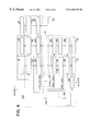
- FIG. 1 is a circuit block diagram of a data monitor circuit 100 of a first embodiment of the present invention.
- FIG. 2 is a circuit block diagram of a data monitor circuit 200 of a second embodiment of the present invention.
- FIG. 3 is a circuit block diagram of a data monitor circuit 300 of a third embodiment of the present invention.
- FIG. 4 is a circuit block diagram of a data monitor circuit 400 of a fourth embodiment of the present invention.
- FIG. 1 is a circuit block diagram of a data monitor circuit 100 of a first embodiment of the present invention.
- the data monitor circuit 100 is embodied as a device internal to a microcomputer.
- FIG. 1 shows the former case where transfers are carried out on the common bus.
- reference numerals 10 and 20 are input output ports commonly used for sending and receiving data etc. between component elements inside the microcomputer (for example the data monitor circuit 100 ) and external components.
- the input output port 10 can be an input port used only for receiving data etc.
- the input output port 20 can be an output port used only for transmitting data etc. in the present invention.
- a first embodiment of the present invention shows that if an input output port is used, the present invention can be applied to a microcomputer having a reduced number of terminals.
- reference numeral 30 is a bus, and has been described above is for commonly transferring address information and data, but it is also possible to respectively provide an address bus for transferring address data and a data bus for transferring data.
- the data monitor circuit 100 is comprised of a data memory address buffer 10 , constituting a first address storage circuit, an address comparator 120 , being a first comparator circuit, an output gate 130 , constituting a first gate circuit, a data buffer 140 , being a first data storage circuit, a controller 150 , constituting a control circuit, and a completion flag section 160 constitution an instruction information storage section.
- address information (address information of the memory for storing data will be called data memory address) of an address of the memory for storing data, not shown, internal to the microcomputer, that is to be monitored, is input from the input output port 10 to the data memory address buffer 110 .
- the data memory address buffer 110 stores and outputs this input address information.
- the test signal T does not designate test (for example, a low level signal)
- a signal input from the input output port 10 is not stored in the data memory address buffer 110 .
- the address comparator 120 compares address information transferred onto the bus 30 during execution of a program and address information stored in the data memory address buffer 110 , and detects coincidence between the two. The result of detection is transferred to the controller 150 as a coincidence signal.
- the coincidence signal indicates that the detected result is no coincidence when at a low level, or that the detection result is coincidence when at a high level.
- the controller 150 outputs an enable signal, being a first permission signal, in response to a coincidence signal from the address comparator 120 . For example, if the coincidence signal is high level, the enable signal becomes high level, while if the coincidence signal is low level the enable signal becomes low level.
- the controller 150 sets the completion flag section 160 in response to a high level coincidence signal.
- set means setting a flag that has an initial condition of “0” to “1”.
- Reset of the completion flag section 160 (resetting to the initial condition of “0”) is carried out, for example, in response to the test signal T becoming high level.
- the flag condition of the completion flag section 160 is output so that it can be confirmed from an external terminal, for example, one terminal of the input output port.
- the output gate 130 makes it possible to transfer data that has been transferred onto the bus to the data buffer 140 in response to a high level enable signal. Specifically, when the enable signal is at a low level, data that has been transferred onto the bus is not transferred to the data buffer 140 .
- the data buffer 140 stores data that has been transferred through the output gate 130 , and outputs it to the input output port 20 .
- the stored contents of the data buffer 140 are preferably initialized (to information that has no effect on normal operation) by receiving a high level test signal T.
- the test signal T When the microcomputer is operating normally, the test signal T is at a low level, and information of an address to be monitored is not stored in the data memory address buffer 110 (or invalid address information not designated in normal operation is stored). As a result, a coincidence signal of the address comparator 120 is always at a low level. Accompanying this, an enable signal of the controller 150 is set to a low level. As a result, there is no transfer of data from the output gate 130 to the data buffer 140 . The input output port 10 and input output port 20 can carry out sending and receiving of data during normal operation, without being affected by the data monitor circuit 100 . At this time, the completion flag also remains at “0”, and is not changed. If there is also a terminal indicating the condition of the flag of the completion flag section 160 at one input/output port, there is no problem since sending and receiving of signals at that input/output port is given priority.
- a test signal T is set to a high level, and memory cell address information of the address of the memory for storing data that is to be monitored is input from the input output port 10 .
- This address information is stored in the data memory address buffer 110 .
- the completion flag section 160 is also reset to an initial state of “0”.
- test signal T is returned to a low level, and similarly to the normal operation, an internal program is executed and the microcomputer operates. With progression of the program, data is read from and written to the memory for storing data, which is the subject of monitoring. At this time, address information has been transferred to the memory for storing data via a bus when reading or writing is carried out, and so the address comparator 120 compares this address information with address information stored in the data memory address buffer 110 .
- a high level coincidence signal is output from the address comparator 120 .
- the controller 150 sets an enable signal to high level in response to the high level coincidence signal.
- the output gate 130 transfers data that has been transferred to the bus and written to the data storage memory (or data that has been read) to the data buffer 140 , based on the coincident address information. This data is stored in the data buffer 140 , and output to the input output port 20 .
- the controller 150 sets the flag for the completion flag section 160 to “1” in response to receipt of the high level coincidence signal. While the address comparator 120 is detecting lack of coincidence, the coincidence signal and the enable signal remain at a low level, and the completion flag section 160 also keeps the flag at “0”.
- the first embodiment of the present invention does not significantly increase the number of structural elements of a data monitor circuit, and does not have complicated control, which means that it can be simply applied, and even if this data monitor circuit is built in, there is no increase in chip size.
- FIG. 2 is a circuit diagram of a data monitoring circuit 200 of a second embodiment of the present invention.
- the same reference numerals are attached to parts that are the same as those of FIG. 1 .
- the data monitoring circuit 200 additionally comprises a program memory address buffer 210 , constituting a second address storage circuit, an address comparator 220 , constituting a second comparison circuit, and an output gate 230 , constituting a second gate circuit, and has a control section 250 modified according to these additional components.
- the program memory address buffer 210 When test is instructed by a test signal T (for example, a high level signal), the program memory address buffer 210 inputs address information to be monitored of the memory for storing program data, not shown, housed in the microcomputer, from an input output port 50 provided in the microcomputer (the address information of the memory for storing a program is also called program memory address).
- the program memory address buffer 210 stores the input address information and outputs it.
- the address comparator 220 compares the address information stored in the program memory address buffer 210 and the address information indicated by the program counter 60 , and detects coincidence.
- the program counter 60 is used when a program is executed, and indicates address information, in the memory for storing the program, where a process to be executed is stored.
- the result of detection of coincidence between the two addresses is transferred to the control section 250 as a coincidence signal. If the coincidence signal is a low level, for example, the detection result indicates lack of coincidence, while if the coincidence signal is a high level the detection result indicates coincidence.
- the control section 250 also functions to output an enable signal, being a first permission signal, in response to the coincidence signal from the address comparator 120 , and outputs an enable signal being a second permission signal in response to a coincidence signal from the address comparator 220 .
- the coincidence signal from the address comparator 220 is, for example, a high level (coincidence detected) the enable signal that is the second permission signal becomes a high level, and when the coincidence signal is low level (lack of coincidence detected) the enable signal becomes a low level.
- control section 250 sets the flag of the completion flag section 160 to “1”.
- the output gate 230 When the enable signal that is the second permission signal (that is, the enable signal corresponding the coincidence detection by the address comparator 220 ) is a high level, the output gate 230 outputs the data stored in the data buffer 140 to the input output port 20 . That is, when the enable signal that is the second permission signal is a low level, the address comparator 220 does not output data that has been stored in the to the input output port 20 .
- the test signal T is a low level, and address information to be monitored is not stored in the data memory address buffer 110 and the program memory address buffer 210 (or alternatively, not specified invalid address information is stored).
- the coincidence signals of the address comparator 120 and address comparator 220 are respectively always at a low level. This in turn means that the two enable signals of the control section 250 become low level.
- there is no transfer of data from the output gate 130 to the data buffer 140 and also data of the data buffer 140 is not transferred from the output gate 230 to the input output port 20 . It is thus possible to carry out normal sending and receiving of data during normal operation, without being affected by the data monitoring circuit 200 .
- the completion flag also remains at “0” and is not changed. This means that even if a terminal indicating the flag condition of the completion flag section 160 is at one input output port, sending and receiving of signals at that input output port is given priority so there is no problem.
- the test signal T is set to a high level, address information of an address value that is desired to be monitored is input from the input output port 50 , and this address information is stored in the data memory address buffer 110 . Under the condition that a specified process is being executed, address information of the program storage memory where the specified process is stored is similarly input from the input output port 50 . This address information is stored in the program memory address buffer 210 . At this time, the completion flag section 160 is also reset to the initial condition of “0”.
- test signal T is returned to a low level, and similarly to the normal operation an internal program is caused to execute and the microcomputer is operated.
- data is read from and written to the data storage memory which is the subject of monitoring.
- address information has been transferred to the memory for storing data via a bus when reading or writing is carried out, and so the address comparator 120 compares this address information with address information stored in the data memory address buffer 110 .
- comparison of address information indicated by the program counter 60 and address information stored in the program memory address buffer 210 is carried out in the address comparator 220 .
- a high level coincidence signal is output.
- the controller 250 sets an enable signal for the output gate 130 to a high level in response to the high level coincidence signal.
- the output gate 130 transfers data that has been transferred to the bus and written to the data storage memory (or data that has been read) to the data buffer 140 , based on the coincident address information.
- a high level enable signal making it possible for the output gate 230 to transfer data is not supplied from the control section 250 (that is, the enable signal supplied to the output gate 230 remains at a low level).
- the completion flag section 160 also maintains the flag at “0”. That is, unless the address comparator 220 detects coincidence, the contents of the data buffer 140 are updated each time the address comparator 120 detects coincidence.
- a high level coincidence signal is output from the address comparator 220 .
- the control section 250 sets an enable signal for the output gate 230 to a high level in response to the high level coincidence signal.
- the output gate 230 outputs data stored in the data buffer 140 at this time to the input output port 20 .
- the control section 250 sets the flag for the completion flag section 160 to “ 1 ” in response to the coincidence signals of the two address comparators 120 and 220 respectively becoming high level.
- the data monitoring circuit 200 of the second embodiment of the present invention it is possible to monitor data that has been written to and read from particular address information of a memory to be monitored until a specified process is executed, which means that it is possible to monitor under more restricted conditions. Accordingly, analysis of defects can be carried out more reliably and in a shorter time.
- FIG. 3 is a circuit diagram of a data monitoring circuit 300 of the third embodiment of the present invention.
- parts that are the same as those in FIG. 2 have the same reference numerals attached thereto.
- the feature of the third embodiment in FIG. 3 is that an address buffer selector 310 , constituting a first selector circuit, a plurality of program memory address buffers 320 , 330 and 340 constituting a second address information circuit as a duplicate storage section (in FIG. 3 there are three, in order to simplify the description), and an address buffer selector 350 , constituting a second selector circuit, are added to the structure of the data monitor circuit, and there is also a control section 360 modified in accordance with these additional components.
- the address buffer selector 310 sequentially selects one of the program memory address buffers 320 , 330 and 340 using a select signal S, and outputs address information to be monitored of a program memory, not shown, housed in the microcomputer, input from the input output port 50 , to the one program memory address buffer that has been selected. If a signal having two-bit information, for example, is used as the select signal S it is possible to select 3 program memory address buffers, but this is not limiting. For example, if the select signal S is a one-bit signal, like a clock signal, the selected object can be switched depending on a number of pulses. In this case, it is possible to use the test signal T in place of the select signal S.
- program memory address buffers 320 , 330 and 340 are instructed to test by a respective test signal T (for example, a high level signal)
- address information to be monitored of a program memory, not shown, housed in the microcomputer is input from the input output port 50 through the address buffer selector 310 .
- Each of the program memory address buffers 320 , 330 and 340 respectively stores this input address information, and outputs the information.
- the address information to be monitored is sequentially stored in the program memory address buffers 320 , 330 and 340 , in order of highest priority.
- the address buffer selector 350 selects one of the program memory address buffers 320 , 330 and 340 in order and address information output from the selected program memory address buffer is output to the address comparator 220 .
- the address buffer selector 350 selects, for example, the program memory address buffer 320 with the test signal T at a high level. For every coincidence signal from the address comparator 220 the address buffer selector 350 selects the program memory address buffers 330 and 340 in order.
- the control section 360 outputs an enable signal to the output gate 130 under similar conditions to the second embodiment, but for the output gate 230 when a high level coincidence signal has been received three times from the address comparator 220 (namely, when coincidence has been detected for address information respectively stored in the three program memory address buffers 320 , 330 and 340 ), an enable signal for the output gate 230 is set to high level (that is, it is made possible to output data stored in the data buffer 140 to the input output port 20 ).
- This control section 250 in the second embodiment may be used in place of the control section 360 with the above described operation of the control section 360 provided in the address comparator 220 .
- the address comparator 220 detects coincidence, it updates the object to be selected in the address buffer selector 350 using a coincidence signal, separate from the coincidence signal to be transferred to the control section 250 .
- the address comparator 220 transfers a high level coincidence signal to the control section 250 .
- the test signal T is low level, and address information to be monitored is not stored in the data memory address buffer 110 and at least the initially selected program memory address buffer 320 (or, in normal operation, unspecified invalid data is stored).
- the input output ports 10 , 20 and 50 can carry out sending and receiving of data in normal operation without being affected by the data monitoring circuit 300 .
- the completion flag also remains at “0” and does not change. As a result, even if a terminal indicating the flag condition of the completion flag section 160 is at one input output port, sending and receiving of signals at that input output port is given priority so there is no problem.
- the test signal T is set to a high level, address information of a memory cell to be monitored of the data storage memory is input from the input output port 10 , and this address information is stored in the data memory address buffer 110 .
- address information of a program storage memory where a first process is stored is first of all input from the input output port 50 and this address information is stored in the program memory address buffer 320 .
- address information of the program storage memory where a third process is stored is input, and this address information is stored in the program memory address buffer 340 . It is possible to realize this storage using the above described operation of the address buffer selector 310 . At this time, the completion flag section 160 is also reset to the initial state of “0”.
- test signal T is returned to a low level, and similarly to the normal operation an internal program is executed to operate the microcomputer.
- data is read from and written to the data storage memory, which is the subject of monitoring.
- the address comparator 120 compares this address information with address information stored in the data memory address buffer 110 .
- comparison of address information indicated by the program counter and address information stored in the program memory address buffer 320 that is initially selected by the address buffer selector 350 is carried out in the address comparator 220 .
- a high level coincidence signal is output.
- the controller 360 sets an enable signal for the output gate 130 to high level in response to the high level coincidence signal.
- the output gate 130 transfers data that has been transferred to the bus and written to the data storage memory (or data that has been read) to the data buffer 140 , based on the coincident address information.
- a high level enable signal making it possible for the output gate 230 to transfer data is not supplied from the control section 360 (that is, the enable signal supplied to the output gate 230 remains at a low level).
- the completion flag section 160 also maintains the flag at “0”. That is, unless the address comparator 220 detects coincidence, the contents of the data buffer 140 are updated each time the address comparator 120 detects coincidence.
- a high level coincidence signal is output from the address comparator 220 .
- the high level coincidence signal is transferred to the control section 360 .
- the control section 360 memorizes receipt of the first coincidence signal from the address comparator 220 . In this case, the control section 360 keeps the enable signal for the output gate 230 at a low level.
- the output gate 230 does not output data stored in the data buffer 140 at this time to the input output port 20 .
- the address buffer selector 350 switches address information transferred to the address comparator 220 to the address information stored in the program memory address buffer 330 .
- the address comparator 220 commences coincidence detection again, and until coincidence is detected for address information stored in all of the program memory address buffers 320 , 330 and 340 , the contents of the data buffer 140 are updated each time the address comparator 120 detects coincidence.
- This type of coincidence detection by the address comparator 220 is carried out sequentially for the program memory address buffers 320 , 330 and 340 by switching the subject program memory address buffer every time coincidence is detected.
- a high level coincidence signal is output from the address comparator 220 .
- the high level coincidence signal is input to the control section 360 .
- a high level coincidence signal output from the address comparator 220 at this time is the third occurrence of coincidence, and so the control section 360 sets an enable signal for the output gate 230 to a high level.
- the output gate 230 outputs data stored in the data buffer 140 a this time to the input output port 20 .
- the control section 360 sets the flag for the completion flag section 160 to “1”.
- the data monitoring circuit 300 of the third embodiment of the present invention after the execution of a few fixed processes and until a specified process is executed, it is possible to output data written to or read from specified address information of a memory to be monitored, which makes it possible to carry out monitoring under more limited conditions (conditions depending on the process). Accordingly, defect analysis can be carried out more reliably and in a shorter time.
- FIG. 4 is a circuit diagram of the data monitoring circuit 400 of the fourth embodiment.
- parts that are the same as in FIG. 2 have the same reference numerals attached thereto.
- FIG. 4 The feature of FIG. 4 is that compared to the data monitoring circuit 200 of FIG. 2, a data memory address buffer 410 , an address comparator 420 , an output gate 460 , a data buffer 470 , an output gate 480 and a data buffer valid flag section 440 are added, and there is also a control section 450 modified in accordance with these additional components.
- the data memory address buffer 410 has the same function as the data memory address buffer 110 , and stores address information to be monitored of the data storage memory that is input from the input output port 70 .
- the address comparator 420 has the same function as the address comparator 120 , and compares the address information stored in the data memory address buffer 410 with the address information transferred to the bus to detect coincidence.
- the control section 450 outputs respectively corresponding high level enable signals in response to coincidence detection by the address comparators 120 and 420 (output of respective high level coincidence signals from each of the address comparators when coincidence is detected).
- the control section 450 outputs respective low level enable signals.
- the control section 450 transfers information indicating a coincidence detection condition (only address comparator 120 detects coincidence, only address comparator 420 detects coincidence, both address comparators detect coincidence, or both address comparators detect lack of coincidence) of the address comparators 120 and 420 to the data buffer valid flag section 440 .
- This information is preferably at least two-bit information.
- the address comparator 220 detects coincidence, transfer of this information is from the control section 450 to the data buffer valid flag section 440 .
- the contents of the data buffer valid flag section 440 are initialized by the test signal T (to “00”, for example) and output from an external terminal of the microcomputer, for example an input output port.
- the output gate 460 has the same function as the output gate 130 , and outputs data transferred to the bus to the data buffer 470 in response to a high level enable signal output from the control section 450 in response to detection of coincidence by the address comparator 420 . That is, when a low level enable signal indicates that the address comparator 420 is detecting lack of coincidence, data transferred to the bus is not output to the data buffer 470 .
- the data buffer 470 has the same function as the data buffer 140 , and stores data transferred through the output gate 460 and outputs this data.
- the output gate 480 has the same function as the output gate 230 , and receives an enable signal output from the control section 450 in response to a high level coincidence signal output when the address comparator 220 detects coincidence, and outputs data stored in the data buffer 470 to the input output port 80 . That is, when a low level enable signal output from the control section 450 is received while the address comparator 220 is detecting lack of coincidence, the output gate 480 does not output data stored in the data buffer 470 .
- the enable signal output from the output gate 480 is the same as the enable signal input to the output gate 230 .
- the data monitoring circuit 400 of the fourth embodiment comprises a first address storage circuit comprised of a plurality (in order to simplify the specification, two in FIG. 4) of duplicate storage sections (data memory address buffers 110 , 410 ), and accompanying these storage sections there are also plurally provided (according to the number of duplicate storage sections) a first comparison circuit (address comparators 120 , 420 ), a first gate circuit (output gates 130 , 460 ), a first data storage circuit (data buffers 140 , 470 ), and a second gate circuit (output gates 230 , 480 ).
- a first comparison circuit address comparators 120 , 420
- first gate circuit output gates 130 , 460
- first data storage circuit data buffers 140 , 470
- second gate circuit output gates 230 , 480
- the test signal is low level and the data memory address buffers 110 and 410 are not storing address information to be monitored (or, invalid address information that is not designated during normal operation) is stored.
- data transfer from the output gate 130 to the data buffer 140 and data transfer from the output gate 460 to the data buffer 470 is not carried out, and there is no transfer of data of the data buffer 140 from the output gate 230 to the input output port 20 , and no transfer of data of the data buffer 470 from the output gate 480 to the input output port 80 . It is possible for the input output ports 10 , 20 , 50 , 70 and 80 to send and receive data during normal operation without being affected by the data monitoring circuit 400 .
- the completion flag also remains at “0”, and the information of the data buffer valid flag section 440 remains unchanged at “00”. Accordingly, even if a terminal for indicating the flag condition of the completion flag section 160 and the information of the data buffer valid flag section 440 is at the input output port, there is no problem since sending and receiving of signals at that input output port is given priority.
- the test signal T is set to high level, one item of address information of a memory cell that is desired to be monitored is input from the input output port 10 , and this address information is stored in the data memory address buffer 110 . Similarly, another one item of address information of a memory cell that is desired to be monitored is input from the input output port 70 and this address information is stored in the data memory address buffer 410 . Similarly, under the condition that a specified process is being executed, address information of the program storage memory where the specified process is stored is input from the input output port 50 , and this address information is stored in the program memory address buffer 210 . At this time, the completion flag section 160 is also reset to the initial condition of “0” and the information of the data buffer valid flag section 440 is reset to “00”.
- the test signal T is returned to low level, and similarly to the normal operation an internal program is caused to execute and the microcomputer is operated.
- data is read from and written to the data storage memory which is the subject of monitoring.
- address information is transferred via a bus, and the address comparator 120 compares this address information being transferred with address information stored in the data memory address buffer 110 , and the address comparator 420 compares the address information being transferred with the address information stored in the data memory address buffer 410 .
- comparison of address information indicated by the program counter 60 and address information stored in the program memory address buffer 210 is carried out in the address comparator 220 .
- the controller 350 sets an enable signal for the output gate 130 (or 460 ) to high level in response to the high level coincidence signal.
- the output gate 130 transfers data that has been transferred to the bus and written to the data storage memory (or data that has been read) to the data buffer 140 (or 470 ), based on the coincident address information.
- the address comparator 220 when the address comparator 220 is not detecting coincidence of address information, a high level enable signal making it possible for the output gates 230 and 480 to transfer data is not supplied from the control section 250 (that is, the enable signal supplied to the output gates 230 and 480 remains at a low level). As a result, data stored in the data buffer 140 (or 470 ) is not output to the input output port 20 (or 80 ). The completion flag section 160 also maintains the flag at “0” and the data buffer valid flag section remains at “00”. That is, unless the address comparator 220 detects coincidence, the contents of the data buffer 140 (or 470 ) are updated each time the address comparator 120 (or 420 ) detects coincidence.
- a high level coincidence signal is output.
- the control section 450 sets an enable signal for the output gates 230 and 480 to a high level in response to the high level coincidence signal.
- the output gates 230 and 480 respectively output data stored in the data buffers 140 and 470 at this time to the input output ports 20 and 80 .
- the control section 450 sets the flag for the completion flag section 160 to “1” in response to the coincidence signals of the three address comparators 120 , 420 and 220 respectively becoming high level.
- the information of the data buffer valid flag section 440 becomes “01”. If the address comparator 420 has also already detected coincidence and the address comparator 120 has not detected coincidence even once before the address comparator 220 detects coincidence, the information of the data buffer valid flag section 440 becomes “10”. If the address comparators 120 and 420 have already detected coincidence before the address comparator 220 detects coincidence, the information of the data buffer valid flag section 440 becomes “11”. The function of this data buffer valid flag section 440 can also be incorporated into the completion flag section 160 .
- the data monitor circuit of present invention is not limited to the structure of the embodiments.
- the data memory address buffer and program memory address buffer etc. are not limited in number to those described in the embodiments above.
- the inputs and outputs to each of the buffers have been described using input output ports, but it goes without saying that inputs and outputs can be connected at other terminals.
- the data monitor circuit of the present invention has been described as being built into a microcomputer, but an external device can also be used as long as the same operation as the data monitor circuit of the present invention is possible.
- the data storage memory that is the subject of monitoring is required to at least read data.
- it is possible to apply a combination of the features of each of the embodiments for example, a data monitor circuit having the respective features of the third embodiment and the fourth embodiment).
Abstract
Description
Claims (10)
Applications Claiming Priority (2)
| Application Number | Priority Date | Filing Date | Title |
|---|---|---|---|
| JP02313198A JP4008086B2 (en) | 1998-02-04 | 1998-02-04 | Data monitor circuit |
| JP10-023131 | 1998-02-04 |
Publications (1)
| Publication Number | Publication Date |
|---|---|
| US6289470B1 true US6289470B1 (en) | 2001-09-11 |
Family
ID=12101986
Family Applications (1)
| Application Number | Title | Priority Date | Filing Date |
|---|---|---|---|
| US09/192,593 Expired - Lifetime US6289470B1 (en) | 1998-02-04 | 1998-11-17 | Data monitor circuit |
Country Status (2)
| Country | Link |
|---|---|
| US (1) | US6289470B1 (en) |
| JP (1) | JP4008086B2 (en) |
Cited By (6)
| Publication number | Priority date | Publication date | Assignee | Title |
|---|---|---|---|---|
| US6636925B1 (en) * | 1999-10-14 | 2003-10-21 | Nec Electronics Corporation | Bus interface circuit preparation apparatus and recording medium |
| US20050121526A1 (en) * | 2003-12-09 | 2005-06-09 | Intelleflex Corporation | Battery activation circuit |
| US20060179354A1 (en) * | 2005-02-09 | 2006-08-10 | Agilent Technologies, Inc. | Two step data analysis |
| US20060215481A1 (en) * | 1998-09-14 | 2006-09-28 | Dally William J | System and method for re-ordering memory references for access to memory |
| EP2472408A1 (en) * | 2010-11-12 | 2012-07-04 | Shenzhen State Micro Technology Co., Ltd | Bus monitor for improving system safety of system on chip (soc) and realizing method thereof |
| WO2013184125A1 (en) * | 2012-06-08 | 2013-12-12 | Hewlett-Packard Development Company, L.P. | Checkpointing using fpga |
Citations (10)
| Publication number | Priority date | Publication date | Assignee | Title |
|---|---|---|---|---|
| US3579199A (en) * | 1969-02-03 | 1971-05-18 | Gen Motors Corp | Method and apparatus for fault testing a digital computer memory |
| US4326290A (en) * | 1979-10-16 | 1982-04-20 | Burroughs Corporation | Means and methods for monitoring the storage states of a memory and other storage devices in a digital data processor |
| US4692897A (en) * | 1984-09-04 | 1987-09-08 | Gte Communication Systems Corporation | Arrangement for dynamic range checking or matching for digital values in a software system |
| JPH02105945A (en) | 1988-10-14 | 1990-04-18 | Mitsubishi Electric Corp | Microcomputer with trigger output |
| US5054026A (en) * | 1988-08-12 | 1991-10-01 | Nec Corporation | Microprocessor having functional redundancy monitoring mode of operation |
| US5263143A (en) * | 1988-07-11 | 1993-11-16 | Star Semiconductor Corporation | Real time probe device for internals of signal processor |
| US5838898A (en) * | 1994-09-14 | 1998-11-17 | Nec Corporation | Microprogram controlled data processing system having a runaway monitor function |
| US6134676A (en) * | 1998-04-30 | 2000-10-17 | International Business Machines Corporation | Programmable hardware event monitoring method |
| US6141757A (en) * | 1998-06-22 | 2000-10-31 | Motorola, Inc. | Secure computer with bus monitoring system and methods |
| US6158028A (en) * | 1997-08-06 | 2000-12-05 | Nec Corporation | Semiconductor integrated circuit |
-
1998
- 1998-02-04 JP JP02313198A patent/JP4008086B2/en not_active Expired - Fee Related
- 1998-11-17 US US09/192,593 patent/US6289470B1/en not_active Expired - Lifetime
Patent Citations (10)
| Publication number | Priority date | Publication date | Assignee | Title |
|---|---|---|---|---|
| US3579199A (en) * | 1969-02-03 | 1971-05-18 | Gen Motors Corp | Method and apparatus for fault testing a digital computer memory |
| US4326290A (en) * | 1979-10-16 | 1982-04-20 | Burroughs Corporation | Means and methods for monitoring the storage states of a memory and other storage devices in a digital data processor |
| US4692897A (en) * | 1984-09-04 | 1987-09-08 | Gte Communication Systems Corporation | Arrangement for dynamic range checking or matching for digital values in a software system |
| US5263143A (en) * | 1988-07-11 | 1993-11-16 | Star Semiconductor Corporation | Real time probe device for internals of signal processor |
| US5054026A (en) * | 1988-08-12 | 1991-10-01 | Nec Corporation | Microprocessor having functional redundancy monitoring mode of operation |
| JPH02105945A (en) | 1988-10-14 | 1990-04-18 | Mitsubishi Electric Corp | Microcomputer with trigger output |
| US5838898A (en) * | 1994-09-14 | 1998-11-17 | Nec Corporation | Microprogram controlled data processing system having a runaway monitor function |
| US6158028A (en) * | 1997-08-06 | 2000-12-05 | Nec Corporation | Semiconductor integrated circuit |
| US6134676A (en) * | 1998-04-30 | 2000-10-17 | International Business Machines Corporation | Programmable hardware event monitoring method |
| US6141757A (en) * | 1998-06-22 | 2000-10-31 | Motorola, Inc. | Secure computer with bus monitoring system and methods |
Cited By (13)
| Publication number | Priority date | Publication date | Assignee | Title |
|---|---|---|---|---|
| US7707384B1 (en) | 1998-09-14 | 2010-04-27 | The Massachusetts Institute of Technology University | System and method for re-ordering memory references for access to memory |
| US20060215481A1 (en) * | 1998-09-14 | 2006-09-28 | Dally William J | System and method for re-ordering memory references for access to memory |
| US7216214B2 (en) * | 1998-09-14 | 2007-05-08 | The Massachusetts Institute Of Technology | System and method for re-ordering memory references for access to memory |
| US6636925B1 (en) * | 1999-10-14 | 2003-10-21 | Nec Electronics Corporation | Bus interface circuit preparation apparatus and recording medium |
| US20050121526A1 (en) * | 2003-12-09 | 2005-06-09 | Intelleflex Corporation | Battery activation circuit |
| US7612652B2 (en) * | 2003-12-09 | 2009-11-03 | Intelleflex Corporation | Battery activation circuit |
| US7333964B2 (en) | 2005-02-09 | 2008-02-19 | Agilent Technologies Inc. | Two step data analysis |
| EP1691273A1 (en) * | 2005-02-09 | 2006-08-16 | Agilent Technologies, Inc. | Two step data analysis |
| US20060179354A1 (en) * | 2005-02-09 | 2006-08-10 | Agilent Technologies, Inc. | Two step data analysis |
| EP2472408A1 (en) * | 2010-11-12 | 2012-07-04 | Shenzhen State Micro Technology Co., Ltd | Bus monitor for improving system safety of system on chip (soc) and realizing method thereof |
| EP2472408A4 (en) * | 2010-11-12 | 2013-07-31 | Shenzhen State Micro Tech Co | Bus monitor for improving system safety of system on chip (soc) and realizing method thereof |
| WO2013184125A1 (en) * | 2012-06-08 | 2013-12-12 | Hewlett-Packard Development Company, L.P. | Checkpointing using fpga |
| US10467116B2 (en) | 2012-06-08 | 2019-11-05 | Hewlett Packard Enterprise Development Lp | Checkpointing using FPGA |
Also Published As
| Publication number | Publication date |
|---|---|
| JPH11219321A (en) | 1999-08-10 |
| JP4008086B2 (en) | 2007-11-14 |
Similar Documents
| Publication | Publication Date | Title |
|---|---|---|
| US6259639B1 (en) | Semiconductor integrated circuit device capable of repairing defective parts in a large-scale memory | |
| EP0095928B1 (en) | Pipeline processing apparatus having a test function | |
| US7286422B2 (en) | Memory device with built-in test function and method for controlling the same | |
| US6757854B1 (en) | Detecting faults in dual port FIFO memories | |
| KR100746389B1 (en) | Integrated semiconductor memory with a memory unit for storing addresses of defective memory cells | |
| US6198669B1 (en) | Semiconductor integrated circuit | |
| KR0172347B1 (en) | Parallel test circuit of semiconductor memory equipment | |
| US20050157565A1 (en) | Semiconductor device for detecting memory failure and method thereof | |
| EP0377455B1 (en) | Test mode switching system for LSI | |
| US6289470B1 (en) | Data monitor circuit | |
| US20080288836A1 (en) | Semiconductor integrated circuit capable of testing with small scale circuit configuration | |
| US6625684B1 (en) | Application specific integrated circuit with dual-mode system for externally accessible data buses and visibility buses | |
| US6745341B1 (en) | Information processing apparatus having fault detection for multiplex storage devices | |
| US7013414B2 (en) | Test method and test system for semiconductor device | |
| US6854081B1 (en) | Initializing/diagnosing system in on-chip multiprocessor system | |
| US20090323454A1 (en) | Semiconductor memory device | |
| GB2308045A (en) | Communication unit switching apparatus | |
| US6055611A (en) | Method and apparatus for enabling redundant memory | |
| US7484147B2 (en) | Semiconductor integrated circuit | |
| US6463562B1 (en) | Semiconductor device including macros and its testing method | |
| US8140921B2 (en) | System for elevator electronic safety device | |
| US7191323B2 (en) | Information processing unit selecting one of reset vector addresses | |
| US20030237036A1 (en) | Semiconductor integrated circuit with built-in self-test function and system including the same | |
| US6628141B1 (en) | Integrated circuit having a scan register chain | |
| JPH07321795A (en) | Buffer address management method |
Legal Events
| Date | Code | Title | Description |
|---|---|---|---|
| AS | Assignment |
Owner name: OKI ELECTRIC INDUSTRY CO., LTD., JAPAN Free format text: ASSIGNMENT OF ASSIGNORS INTEREST;ASSIGNOR:TANAKA, TOSHIYUKI;REEL/FRAME:009600/0813 Effective date: 19981109 |
|
| AS | Assignment |
Owner name: WILMINGTON TRUST COMPANY, AS TRUSTEE, DELAWARE Free format text: SECURITY INTEREST;ASSIGNOR:FEDERAL-MOGUL WORLD WIDE, INC. (MI CORPORATION);REEL/FRAME:011466/0001 Effective date: 20001229 |
|
| STCF | Information on status: patent grant |
Free format text: PATENTED CASE |
|
| FPAY | Fee payment |
Year of fee payment: 4 |
|
| AS | Assignment |
Owner name: FEDERAL-MOGUL WORLDWIDE, INC., MICHIGAN Free format text: RELEASE OF SECURITY INTEREST RECORDED AT REEL/FRAME 011571/0001 AND 011466/0001;ASSIGNOR:WILMINGTON TRUST COMPANY, AS TRUSTEE;REEL/FRAME:020299/0377 Effective date: 20071217 |
|
| FPAY | Fee payment |
Year of fee payment: 8 |
|
| AS | Assignment |
Owner name: OKI SEMICONDUCTOR CO., LTD., JAPAN Free format text: CHANGE OF NAME;ASSIGNOR:OKI ELECTRIC INDUSTRY CO., LTD.;REEL/FRAME:022343/0290 Effective date: 20081001 |
|
| FPAY | Fee payment |
Year of fee payment: 12 |
|
| AS | Assignment |
Owner name: LAPIS SEMICONDUCTOR CO., LTD., JAPAN Free format text: CHANGE OF NAME;ASSIGNOR:OKI SEMICONDUCTOR CO., LTD;REEL/FRAME:032495/0483 Effective date: 20111003 |