US6303457B1 - Integrated circuit having integral decoupling capacitor - Google Patents
Integrated circuit having integral decoupling capacitor Download PDFInfo
- Publication number
- US6303457B1 US6303457B1 US08/890,047 US89004797A US6303457B1 US 6303457 B1 US6303457 B1 US 6303457B1 US 89004797 A US89004797 A US 89004797A US 6303457 B1 US6303457 B1 US 6303457B1
- Authority
- US
- United States
- Prior art keywords
- decoupling capacitor
- forming
- conductive film
- metal layer
- final metal
- Prior art date
- Legal status (The legal status is an assumption and is not a legal conclusion. Google has not performed a legal analysis and makes no representation as to the accuracy of the status listed.)
- Expired - Fee Related
Links
Images


Classifications
-
- H—ELECTRICITY
- H01—ELECTRIC ELEMENTS
- H01L—SEMICONDUCTOR DEVICES NOT COVERED BY CLASS H10
- H01L27/00—Devices consisting of a plurality of semiconductor or other solid-state components formed in or on a common substrate
- H01L27/02—Devices consisting of a plurality of semiconductor or other solid-state components formed in or on a common substrate including semiconductor components specially adapted for rectifying, oscillating, amplifying or switching and having at least one potential-jump barrier or surface barrier; including integrated passive circuit elements with at least one potential-jump barrier or surface barrier
- H01L27/04—Devices consisting of a plurality of semiconductor or other solid-state components formed in or on a common substrate including semiconductor components specially adapted for rectifying, oscillating, amplifying or switching and having at least one potential-jump barrier or surface barrier; including integrated passive circuit elements with at least one potential-jump barrier or surface barrier the substrate being a semiconductor body
-
- H—ELECTRICITY
- H01—ELECTRIC ELEMENTS
- H01L—SEMICONDUCTOR DEVICES NOT COVERED BY CLASS H10
- H01L23/00—Details of semiconductor or other solid state devices
- H01L23/52—Arrangements for conducting electric current within the device in operation from one component to another, i.e. interconnections, e.g. wires, lead frames
- H01L23/522—Arrangements for conducting electric current within the device in operation from one component to another, i.e. interconnections, e.g. wires, lead frames including external interconnections consisting of a multilayer structure of conductive and insulating layers inseparably formed on the semiconductor body
- H01L23/5222—Capacitive arrangements or effects of, or between wiring layers
- H01L23/5223—Capacitor integral with wiring layers
-
- H—ELECTRICITY
- H01—ELECTRIC ELEMENTS
- H01L—SEMICONDUCTOR DEVICES NOT COVERED BY CLASS H10
- H01L28/00—Passive two-terminal components without a potential-jump or surface barrier for integrated circuits; Details thereof; Multistep manufacturing processes therefor
- H01L28/40—Capacitors
- H01L28/60—Electrodes
- H01L28/82—Electrodes with an enlarged surface, e.g. formed by texturisation
- H01L28/86—Electrodes with an enlarged surface, e.g. formed by texturisation having horizontal extensions
-
- H—ELECTRICITY
- H01—ELECTRIC ELEMENTS
- H01L—SEMICONDUCTOR DEVICES NOT COVERED BY CLASS H10
- H01L2924/00—Indexing scheme for arrangements or methods for connecting or disconnecting semiconductor or solid-state bodies as covered by H01L24/00
- H01L2924/0001—Technical content checked by a classifier
- H01L2924/0002—Not covered by any one of groups H01L24/00, H01L24/00 and H01L2224/00
Definitions
- the present invention relates generally to the design and fabrication of integrated circuit (IC) chips, and, more particularly, to IC chips having decoupling capacitance.
- IC integrated circuit
- Decoupling capacitors have been provided on chip carriers, modules which carry multiple IC chips. See, e.g., U.S. Pat. No. 5,134,539 to Tuckerman et al. and U.S. Pat. No. 4,675,717 to Herrero et al.
- chip carrier decoupling capacitors do not sufficiently reduce or isolate the power supply bounce on the IC chips which it carries.
- Off-chip decoupling capacitors have been provided with wiring directly to the IC chip.
- the long wire connections have high resistance which necessarily limits the effectiveness of this capacitance due to the excessively large time constant. Also this technique leads to high costs due to discrete capacitor substrate complexity and assembly cost.
- On-chip solutions have been attempted by fabricating parallel plate capacitor structures using two or more metal layers of an integrated circuit.
- Beach et al. High Dielectric Constant On-Chip Decoupling Capacitor Incorporated Into BEOL Fabrication Process, IBM Technical Disclosure Bulletin, October 1994
- a decoupling capacitor is built between the final metal layer and the underlying metal layer.
- U.S. Pat. No. 5,208,725 to Akcasu an integral decoupling capacitor consisting of two sets of parallel conducting strips formed by the existing layers of an integrated circuit is disclosed. These techniques use significant numbers of metal wires that could otherwise be used for signal or logic wiring.
- a third decoupling capacitor fabrication technique utilizes structures built with gate oxide capacitors.
- capacitors occupy a large silicon area of a chip and are prone to stress failure, thereby limiting yield and/or reliability.
- the oxide layer is not as thick as desired, a stress point may develop and, with time, cause the chip to fail.
- the oxide layer may have a thin hole or other defect which could cause the chip to fail immediately.
- these decoupling capacitors are inefficient and expensive.
- the present invention is a decoupling capacitor for an integrated circuit.
- the integrated circuit has a final metal layer which includes a power bus.
- the decoupling capacitor comprises a dielectric film disposed over the final metal layer and a conductive film disposed over the dielectric layer, whereby capacitance may be provided in the dielectric layer.
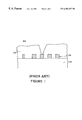
- FIG. 1 is a cross-sectional view of the uppermost layers of a conventional IC chip
- FIG. 2 is a top schematic view of an integrated circuit having a decoupling capacitor in accordance with an exemplary embodiment of the present invention.
- FIGS. 3A-3D are cross-sectional views at various stages of an exemplary fabrication process for forming an integrated circuit having a decoupling capacitor.
- a conventional IC chip 110 typically includes a number of layers, including a number of metal layers.
- the uppermost layers, as shown in FIG. 1, include a final metal layer 120 deposited on a dielectric layer 130 .
- the final metal layer 120 typically carries both signal wires and power distribution wires (power buses).
- Deposited over the final metal layer 120 may be an overcoat layer 150 , typically silicon dioxide, silicon nitride, and/or a polymer.
- the overcoat layer 150 is deposited over a varying topography.
- the final metal layer 20 typically comprises a plurality of signal wires 26 and power buses 22 , 24 .
- the power buses are typically aluminum and include ground buses 22 which are connected to a ground source, e.g. 0 Volts (V), and voltage supply buses 24 , each of which are connected to a voltage source, e.g. 2.5 V, 3.3 V, 5.0 V, etc.
- a voltage source e.g. 2.5 V, 3.3 V, 5.0 V, etc.
- the decoupling capacitor 12 comprises a dielectric film 30 disposed between the final metal layer 20 and a conductive film 40 .
- the final metal layer 20 forms one plate of the decoupling capacitor 12 while the conductive film 40 forms the other.
- the conductive film 40 may be selectively patterned over the surface of the IC chip 10 so as to allow connections to the underlying final metal layer 20 and to form decoupling capacitance only where desired.
- the provision of capacitance directly above the final metal layer 20 enhances the performance of IC chips.
- the wire connections to the capacitor plates are shorter than the wire connections in off-chip decoupling capacitors.
- the decoupling capacitor 12 allows higher switching speeds in IC chips by providing faster response to power supply bounce resulting from the large currents required by high speed switching.
- FIGS. 3A through 3D there is illustrated an exemplary process for fabricating an IC chip 10 having an integral decoupling capacitor 12 .
- the final metal layer 20 is deposited and defined on the IC chip 10 .
- the structure of the IC chip 10 at this stage is shown in FIG. 3 A.
- a dielectric film 30 is disposed over the final metal layer 20 .
- the dielectric film 30 may be placed over a mechanically polished surface exposing the final metal layer 20 .
- the final metal layer 20 is not polished, as polishing adds a process step, and, more importantly, a non-polished surface enables the decoupling capacitor 12 to take advantage of the sides 21 of the final metal layer 20 wires to increase the capacitance as will be described more fully hereinafter.
- the dielectric film 30 is a relatively high dielectric constant material, typically silicon nitride or silicon oxide, or another frequently used material such as a polyimide or other polymer.
- the dielectric film 30 may be disposed over the final metal layer using a number of techniques, including evaporation, sputtering, or chemical vapor deposition.
- the dielectric film 30 comprises silicon nitride, deposited by chemical vapor deposition. Silicon nitride provides a relatively high dielectric constant and reliable performance.
- the dielectric film 30 may be deposited to a substantially uniform thickness over the surface of the IC chip 10 and should sufficiently cover the final metal layer 20 so as to avoid the formation of voids which may cause shorting of the final metal layer 20 wires after the conductive film 40 is applied. It is noted that the uniform thickness may vary somewhat as a result of deposition over a varying topography. For example, as illustrated in FIG. 3C, the dielectric film 30 may be thicker on flat surfaces 32 on top of and between final metal wires than on side wall surfaces 34 adjacent the sides 21 of the final metal wires.
- the conductive film 40 is selectively placed over the surface of the IC chip 10 .
- the conductive film 40 is deposited over substantially all of the surface of the IC chip 10 , for example, by evaporation or sputtering. Then, using photolithographic techniques, the conductive film 40 is etched to remove the conductive film 40 where desired. As best shown in FIGS. 2 and 3B, the conductive film 40 is selectively etched from the areas around the signal wires 26 and also etched to form gaps 27 over portions of the final metal layer 20 . The conductive film 40 is not disposed over the signal wires 26 , because capacitance impedes the switching of the signal wires 26 . The etched gaps 27 are provided to enable the final metal layer 20 to be connected to a power source as more fully described hereinbelow.
- the conductive film 40 is connected to a supply voltage opposite that of an underlying power bus 22 , 24 .
- the conductive film 40 comprises two conductive strips 42 , 44 , one strip 42 being disposed above ground buses 22 and connected to a voltage supply source, the other strip 44 being disposed above voltage supply buses 24 and connected to ground.
- the use of two conductive strips is by way of example, not of limitation.
- each power bus or grouping thereof could be associated with a conductive strip connected to an opposite supply voltage.
- the conductive film 40 may be etched as shown in FIG. 2, with gaps 47 isolating and defining the conductive strips.
- the resulting conductive film 40 substantially covers all of the power buses 22 , 24 of the final metal layer 20 , but the etched gaps 27 which are used for terminal connections to the final metal layer 20 .
- terminal connections represent less than 1 percent (%) of the area of an IC chip whereas the final metal layer 20 covers a substantial portion, e.g. 70-75%, of the chip.
- the conductive film 40 is deposited over a non-polished dielectric film 30 . This allows the conductive film 40 to surround the sides 21 , as well as the top, of the final metal wires. This presents a three-sided capacitor with increased surface area and thus increased capacitance.
- an overcoat layer 50 typically silicon nitride silicon dioxide and/or a polymer, may be deposited by conventional means, e.g., by chemical vapor deposition.
- an overcoat layer 50 typically silicon nitride silicon dioxide and/or a polymer
- openings are provided through the overcoat layer to establish vias 53 which connect power sources to the conductive film 40 and the power buses 22 , 24 and signal wires 26 of the final metal layer 20 .
- FIGS. 2 and 3D A top schematic view and a side, cross-sectional view of portions of exemplary final structures are shown in FIGS. 2 and 3D. Vias 53 which connect the power buses 22 , 24 are provided through the etched gaps 27 formed in the conductive film 40 .
- the dielectric film 30 has a flat surface 32 thickness on the order of 1500 A and a side wall 34 thickness on the order of 1100 A. It is noted that the dielectric film 30 may have any thickness, with thinner films being less reliable and thicker films generally not providing sufficient capacitance per unit area.
- the conductive film 40 may have a thickness on the order of 2000 A.
- the conductive film 40 thickness may range from 1000 A and upward, though thinner films 40 result in more resistance.
- the thickness of the conductive film 40 is limited by the distance between the power buses 22 , 24 .
- the overall decoupling capacitance provided by the present invention varies with the number and size of the power buses 22 , 24 , with IC chips having more, narrower buses 22 , 24 providing higher decoupling capacitance.
- the integral decoupling capacitor of the present invention in addition to enhancing chip performance, reduces the cost of the packaged chip relative to chips incorporating other decoupling techniques.
- the integral decoupling capacitor 12 may replace existing gate level capacitors, increasing reliability and reducing silicon area, and thus reducing cost.
- the decoupling capacitor 12 may also be used in conjunction with existing gate level capacitors and/or external decoupling capacitors, if so desired. In the latter instance, if an existing chip design lacks sufficient decoupling capacitance, an integral decoupling capacitor 12 may be easily incorporated into the manufacturing process without requiring a redesign of the underlying layers of the IC chip and/or the bulk of the manufacturing process.
- the integral decoupling capacitor may be employed on other devices, such as chip-carrying substrates. Accordingly, the scope of the present invention should not be limited to the particular embodiments discussed above, but should be defined only by full and fair scope of the claims set forth below.
Abstract
The present invention is a decoupling capacitor for an integrated circuit. The integrated circuit has a final metal layer which includes a power bus. The decoupling capacitor comprises a dielectric film disposed over the final metal layer and a conductive film disposed over the dielectric layer, whereby capacitance may be provided in the dielectric layer.
Description
This is a Divisional of application Ser. No. 08/600,533, filed Feb. 13, 1996, U.S. Pat. No. 5,872,697, which application(s) are incorporated herein by reference.
The present invention relates generally to the design and fabrication of integrated circuit (IC) chips, and, more particularly, to IC chips having decoupling capacitance.
As silicon device geometries shrink, IC chip densities and speed performance improve considerably. Systems with these devices switch in subnanosecond times with further advances in chip densities and performance being expected. This high speed switching results in high transient currents which cause supply voltage variations, generally known as power supply bounce. In response, decoupling capacitors have generally been used to isolate the devices from the power supply bounce.
Decoupling capacitors have been provided on chip carriers, modules which carry multiple IC chips. See, e.g., U.S. Pat. No. 5,134,539 to Tuckerman et al. and U.S. Pat. No. 4,675,717 to Herrero et al. However, due to the rapidly shrinking sizes and rapidly increasing speeds of integrated circuits, chip carrier decoupling capacitors do not sufficiently reduce or isolate the power supply bounce on the IC chips which it carries. Off-chip decoupling capacitors have been provided with wiring directly to the IC chip. However, the long wire connections have high resistance which necessarily limits the effectiveness of this capacitance due to the excessively large time constant. Also this technique leads to high costs due to discrete capacitor substrate complexity and assembly cost.
On-chip solutions have been attempted by fabricating parallel plate capacitor structures using two or more metal layers of an integrated circuit. For example, in Beach et al., High Dielectric Constant On-Chip Decoupling Capacitor Incorporated Into BEOL Fabrication Process, IBM Technical Disclosure Bulletin, October 1994, a decoupling capacitor is built between the final metal layer and the underlying metal layer. In U.S. Pat. No. 5,208,725 to Akcasu, an integral decoupling capacitor consisting of two sets of parallel conducting strips formed by the existing layers of an integrated circuit is disclosed. These techniques use significant numbers of metal wires that could otherwise be used for signal or logic wiring. A third decoupling capacitor fabrication technique utilizes structures built with gate oxide capacitors. These capacitors occupy a large silicon area of a chip and are prone to stress failure, thereby limiting yield and/or reliability. For example, if the oxide layer is not as thick as desired, a stress point may develop and, with time, cause the chip to fail. In addition, the oxide layer may have a thin hole or other defect which could cause the chip to fail immediately. Thus, these decoupling capacitors are inefficient and expensive.
There is an intensely felt need in the integrated circuit industry to provide a low cost and highly reliable integrated circuit having an integral decoupling capacitor. The present invention addresses this need as well as other needs.
The present invention is a decoupling capacitor for an integrated circuit. The integrated circuit has a final metal layer which includes a power bus. The decoupling capacitor comprises a dielectric film disposed over the final metal layer and a conductive film disposed over the dielectric layer, whereby capacitance may be provided in the dielectric layer.
FIG. 1 is a cross-sectional view of the uppermost layers of a conventional IC chip;
FIG. 2 is a top schematic view of an integrated circuit having a decoupling capacitor in accordance with an exemplary embodiment of the present invention; and
FIGS. 3A-3D are cross-sectional views at various stages of an exemplary fabrication process for forming an integrated circuit having a decoupling capacitor.
Referring now to the drawings, and more particularly to FIG. 1, there is shown a cross-sectional view of the uppermost layers of a conventional integrated circuit (IC) chip 110. As will be appreciated by those skilled in the art, a conventional IC chip 110 typically includes a number of layers, including a number of metal layers. The uppermost layers, as shown in FIG. 1, include a final metal layer 120 deposited on a dielectric layer 130. The final metal layer 120 typically carries both signal wires and power distribution wires (power buses). Deposited over the final metal layer 120 may be an overcoat layer 150, typically silicon dioxide, silicon nitride, and/or a polymer. Though the lower layers of the IC chip 110 are typically mechanically polished to a flat surface, the final metal layer 120 is not. Thus, in conventional IC chips 110, the overcoat layer 150 is deposited over a varying topography.
Turning now to FIG. 3D, there is illustrated an exemplary IC chip 10 having an integral decoupling capacitor, generally designated 12, formed between its final metal layer 20 and an overcoat layer 50. The final metal layer 20 typically comprises a plurality of signal wires 26 and power buses 22, 24. The power buses are typically aluminum and include ground buses 22 which are connected to a ground source, e.g. 0 Volts (V), and voltage supply buses 24, each of which are connected to a voltage source, e.g. 2.5 V, 3.3 V, 5.0 V, etc. For purposes of clarity, only a limited area of the IC chip 10 is depicted in the drawings.
The decoupling capacitor 12 comprises a dielectric film 30 disposed between the final metal layer 20 and a conductive film 40. The final metal layer 20 forms one plate of the decoupling capacitor 12 while the conductive film 40 forms the other. As will be explained more fully hereinafter, the conductive film 40 may be selectively patterned over the surface of the IC chip 10 so as to allow connections to the underlying final metal layer 20 and to form decoupling capacitance only where desired.
The provision of capacitance directly above the final metal layer 20 enhances the performance of IC chips. For example, the wire connections to the capacitor plates are shorter than the wire connections in off-chip decoupling capacitors. Thus, the decoupling capacitor 12 allows higher switching speeds in IC chips by providing faster response to power supply bounce resulting from the large currents required by high speed switching.
Referring now to FIGS. 3A through 3D, there is illustrated an exemplary process for fabricating an IC chip 10 having an integral decoupling capacitor 12. Using conventional prior process steps, the final metal layer 20 is deposited and defined on the IC chip 10. The structure of the IC chip 10 at this stage is shown in FIG. 3A.
Referring now to FIG. 3B, a dielectric film 30 is disposed over the final metal layer 20. The dielectric film 30 may be placed over a mechanically polished surface exposing the final metal layer 20. In the exemplary embodiment, however, the final metal layer 20 is not polished, as polishing adds a process step, and, more importantly, a non-polished surface enables the decoupling capacitor 12 to take advantage of the sides 21 of the final metal layer 20 wires to increase the capacitance as will be described more fully hereinafter. The dielectric film 30 is a relatively high dielectric constant material, typically silicon nitride or silicon oxide, or another frequently used material such as a polyimide or other polymer. The dielectric film 30 may be disposed over the final metal layer using a number of techniques, including evaporation, sputtering, or chemical vapor deposition. In the exemplary embodiment, the dielectric film 30 comprises silicon nitride, deposited by chemical vapor deposition. Silicon nitride provides a relatively high dielectric constant and reliable performance.
The dielectric film 30 may be deposited to a substantially uniform thickness over the surface of the IC chip 10 and should sufficiently cover the final metal layer 20 so as to avoid the formation of voids which may cause shorting of the final metal layer 20 wires after the conductive film 40 is applied. It is noted that the uniform thickness may vary somewhat as a result of deposition over a varying topography. For example, as illustrated in FIG. 3C, the dielectric film 30 may be thicker on flat surfaces 32 on top of and between final metal wires than on side wall surfaces 34 adjacent the sides 21 of the final metal wires.
As noted above, the conductive film 40 is selectively placed over the surface of the IC chip 10. In the exemplary embodiment, the conductive film 40 is deposited over substantially all of the surface of the IC chip 10, for example, by evaporation or sputtering. Then, using photolithographic techniques, the conductive film 40 is etched to remove the conductive film 40 where desired. As best shown in FIGS. 2 and 3B, the conductive film 40 is selectively etched from the areas around the signal wires 26 and also etched to form gaps 27 over portions of the final metal layer 20. The conductive film 40 is not disposed over the signal wires 26, because capacitance impedes the switching of the signal wires 26. The etched gaps 27 are provided to enable the final metal layer 20 to be connected to a power source as more fully described hereinbelow.
To form a decoupling capacitor 12, the conductive film 40 is connected to a supply voltage opposite that of an underlying power bus 22, 24. In the exemplary embodiment shown in FIG. 2, the conductive film 40 comprises two conductive strips 42, 44, one strip 42 being disposed above ground buses 22 and connected to a voltage supply source, the other strip 44 being disposed above voltage supply buses 24 and connected to ground. The use of two conductive strips is by way of example, not of limitation. For example, each power bus or grouping thereof could be associated with a conductive strip connected to an opposite supply voltage.
To form the conductive strips 42, 44, the conductive film 40 may be etched as shown in FIG. 2, with gaps 47 isolating and defining the conductive strips. The resulting conductive film 40 substantially covers all of the power buses 22, 24 of the final metal layer 20, but the etched gaps 27 which are used for terminal connections to the final metal layer 20. However, it should be appreciated that terminal connections represent less than 1 percent (%) of the area of an IC chip whereas the final metal layer 20 covers a substantial portion, e.g. 70-75%, of the chip.
In the exemplary embodiment, the conductive film 40 is deposited over a non-polished dielectric film 30. This allows the conductive film 40 to surround the sides 21, as well as the top, of the final metal wires. This presents a three-sided capacitor with increased surface area and thus increased capacitance.
After the conductive film 40, i.e., the top plate of the decoupling capacitor 12, has been formed, an overcoat layer 50, typically silicon nitride silicon dioxide and/or a polymer, may be deposited by conventional means, e.g., by chemical vapor deposition. At this point, the structure of the IC chip 10 is as shown in FIG. 3C. Next, openings are provided through the overcoat layer to establish vias 53 which connect power sources to the conductive film 40 and the power buses 22, 24 and signal wires 26 of the final metal layer 20. A top schematic view and a side, cross-sectional view of portions of exemplary final structures are shown in FIGS. 2 and 3D. Vias 53 which connect the power buses 22, 24 are provided through the etched gaps 27 formed in the conductive film 40.
In an exemplary embodiment of the present invention, the dielectric film 30 has a flat surface 32 thickness on the order of 1500 A and a side wall 34 thickness on the order of 1100 A. It is noted that the dielectric film 30 may have any thickness, with thinner films being less reliable and thicker films generally not providing sufficient capacitance per unit area.
The conductive film 40 may have a thickness on the order of 2000 A. The conductive film 40 thickness may range from 1000 A and upward, though thinner films 40 result in more resistance. In the exemplary embodiment, the thickness of the conductive film 40 is limited by the distance between the power buses 22, 24. As will be appreciated by those skilled in the art, the overall decoupling capacitance provided by the present invention varies with the number and size of the power buses 22, 24, with IC chips having more, narrower buses 22, 24 providing higher decoupling capacitance.
The integral decoupling capacitor of the present invention, in addition to enhancing chip performance, reduces the cost of the packaged chip relative to chips incorporating other decoupling techniques. The integral decoupling capacitor 12 may replace existing gate level capacitors, increasing reliability and reducing silicon area, and thus reducing cost. The decoupling capacitor 12 may also be used in conjunction with existing gate level capacitors and/or external decoupling capacitors, if so desired. In the latter instance, if an existing chip design lacks sufficient decoupling capacitance, an integral decoupling capacitor 12 may be easily incorporated into the manufacturing process without requiring a redesign of the underlying layers of the IC chip and/or the bulk of the manufacturing process.
It will, of course, be understood that various modifications and additions can be made to the embodiments discussed herein above without parting from the scope or spirit of the present invention. For example, the integral decoupling capacitor may be employed on other devices, such as chip-carrying substrates. Accordingly, the scope of the present invention should not be limited to the particular embodiments discussed above, but should be defined only by full and fair scope of the claims set forth below.
Claims (11)
1. A method of forming an integral decoupling capacitor for an integrated circuit device, comprising the steps of:
providing an integrated circuit device base having a substrate;
forming a final metal layer directly over the substrate, the final metal layer including a plurality of power busses acting as at least one first capacitor plate and a plurality of signal wires, wherein the plurality of signal wires are electrically isolated from the plurality of power busses;
placing a dielectric film over the final metal layer; and
placing a conductive film over the dielectric film, acting as at least one second capacitor plate, wherein the integral decoupling capacitor is formed over the plurality of power busses.
2. The method of forming an integral decoupling capacitor of claim 1, further comprising the step of placing an overcoat layer over the conductive film.
3. The method of forming an integral decoupling capacitor of claim 2, further comprising the step of forming vias to enable connections to the conductive film and the final metal layer.
4. The method of forming an integral decoupling capacitor of claim 1, wherein the dielectric film covers substantially all of the final metal layer of the integrated circuit.
5. The method of forming an integral decoupling capacitor of claim 1, wherein the step of placing the dielectric film comprises depositing the dielectric film by chemical vapor deposition.
6. The method of forming an integral decoupling capacitor of claim 1, wherein the dielectric film is formed to comprise silicon nitride.
7. The method of forming an integral decoupling capacitor of claim 1, wherein the conductive film is formed to cover the top and sides of the plurality of power busses.
8. The method of forming an integral decoupling capacitor of claim 1, wherein the conductive film is formed to comprise at least two conductive strips.
9. The method of forming an integral decoupling capacitor of claim 1, wherein
the final metal layer is formed to include signal wires; and
the conductive film is formed so that it does not cover the plurality of signal wires.
10. The method of forming an integral decoupling capacitor of claim 1, wherein the step of placing the conductive film comprises sputtering the conductive film.
11. The method of forming an integral decoupling capacitor of claim 1, wherein the conductive film is formed to comprise aluminum.
Priority Applications (1)
| Application Number | Priority Date | Filing Date | Title |
|---|---|---|---|
| US08/890,047 US6303457B1 (en) | 1996-02-13 | 1997-07-09 | Integrated circuit having integral decoupling capacitor |
Applications Claiming Priority (2)
| Application Number | Priority Date | Filing Date | Title |
|---|---|---|---|
| US08/600,533 US5872697A (en) | 1996-02-13 | 1996-02-13 | Integrated circuit having integral decoupling capacitor |
| US08/890,047 US6303457B1 (en) | 1996-02-13 | 1997-07-09 | Integrated circuit having integral decoupling capacitor |
Related Parent Applications (1)
| Application Number | Title | Priority Date | Filing Date |
|---|---|---|---|
| US08/600,533 Division US5872697A (en) | 1996-02-13 | 1996-02-13 | Integrated circuit having integral decoupling capacitor |
Publications (1)
| Publication Number | Publication Date |
|---|---|
| US6303457B1 true US6303457B1 (en) | 2001-10-16 |
Family
ID=24403982
Family Applications (2)
| Application Number | Title | Priority Date | Filing Date |
|---|---|---|---|
| US08/600,533 Expired - Lifetime US5872697A (en) | 1996-02-13 | 1996-02-13 | Integrated circuit having integral decoupling capacitor |
| US08/890,047 Expired - Fee Related US6303457B1 (en) | 1996-02-13 | 1997-07-09 | Integrated circuit having integral decoupling capacitor |
Family Applications Before (1)
| Application Number | Title | Priority Date | Filing Date |
|---|---|---|---|
| US08/600,533 Expired - Lifetime US5872697A (en) | 1996-02-13 | 1996-02-13 | Integrated circuit having integral decoupling capacitor |
Country Status (6)
| Country | Link |
|---|---|
| US (2) | US5872697A (en) |
| EP (1) | EP0790649A3 (en) |
| JP (1) | JP3405650B2 (en) |
| KR (1) | KR970063716A (en) |
| CN (1) | CN1102295C (en) |
| TW (1) | TW357427B (en) |
Cited By (15)
| Publication number | Priority date | Publication date | Assignee | Title |
|---|---|---|---|---|
| US20030222698A1 (en) * | 2002-05-30 | 2003-12-04 | Sun Microsystems, Inc. | Process variation compensated high voltage decoupling capacitor biasing circuit with no DC current |
| US20050287718A1 (en) * | 2004-06-29 | 2005-12-29 | International Business Machines Corporation | Integrated soi fingered decoupling capacitor |
| US20060292815A1 (en) * | 2005-06-28 | 2006-12-28 | Roberts Douglas R | MIM capacitor in a semiconductor device and method therefor |
| US20100127347A1 (en) * | 2008-11-21 | 2010-05-27 | Xilinx, Inc. | Shielding for integrated capacitors |
| US20100127309A1 (en) * | 2008-11-21 | 2010-05-27 | Xilinx, Inc. | Integrated capacitor with alternating layered segments |
| US20100127351A1 (en) * | 2008-11-21 | 2010-05-27 | Xilinx, Inc. | Integrated capacitor with interlinked lateral fins |
| US20100127348A1 (en) * | 2008-11-21 | 2010-05-27 | Xilinx, Inc. | Integrated capicitor with cabled plates |
| US20100127349A1 (en) * | 2008-11-21 | 2010-05-27 | Xilinx, Inc. | Integrated capacitor with array of crosses |
| US7994610B1 (en) | 2008-11-21 | 2011-08-09 | Xilinx, Inc. | Integrated capacitor with tartan cross section |
| CN102891142A (en) * | 2011-07-21 | 2013-01-23 | 台湾积体电路制造股份有限公司 | Semiconductor devices with orientation-free decoupling capacitors and methods of manufacture thereof |
| US20130264870A1 (en) * | 2012-04-10 | 2013-10-10 | Sol Chip Ltd. | Integrated circuit energy harvester |
| US8653844B2 (en) | 2011-03-07 | 2014-02-18 | Xilinx, Inc. | Calibrating device performance within an integrated circuit |
| US8941974B2 (en) | 2011-09-09 | 2015-01-27 | Xilinx, Inc. | Interdigitated capacitor having digits of varying width |
| US9270247B2 (en) | 2013-11-27 | 2016-02-23 | Xilinx, Inc. | High quality factor inductive and capacitive circuit structure |
| US9524964B2 (en) | 2014-08-14 | 2016-12-20 | Xilinx, Inc. | Capacitor structure in an integrated circuit |
Families Citing this family (32)
| Publication number | Priority date | Publication date | Assignee | Title |
|---|---|---|---|---|
| USRE38550E1 (en) | 1996-10-18 | 2004-07-06 | California Micro Devices, Inc. | Method for programmable integrated passive devices |
| US5998275A (en) * | 1997-10-17 | 1999-12-07 | California Micro Devices, Inc. | Method for programmable integrated passive devices |
| DE19646208C2 (en) * | 1996-11-08 | 2001-08-30 | Infineon Technologies Ag | Capacitor manufacturing method and memory array |
| JP3060995B2 (en) * | 1997-05-29 | 2000-07-10 | 日本電気株式会社 | Semiconductor capacitive element structure and manufacturing method |
| JP2000216343A (en) * | 1999-01-27 | 2000-08-04 | Nec Corp | Semiconductor integrated circuit |
| US6565730B2 (en) | 1999-12-29 | 2003-05-20 | Intel Corporation | Self-aligned coaxial via capacitors |
| US6278147B1 (en) | 2000-01-18 | 2001-08-21 | International Business Machines Corporation | On-chip decoupling capacitor with bottom hardmask |
| US6323099B1 (en) | 2000-02-02 | 2001-11-27 | Advanced Micro Devices | High k interconnect de-coupling capacitor with damascene process |
| US6417556B1 (en) | 2000-02-02 | 2002-07-09 | Advanced Micro Devices, Inc. | High K dielectric de-coupling capacitor embedded in backend interconnect |
| US6384468B1 (en) | 2000-02-07 | 2002-05-07 | International Business Machines Corporation | Capacitor and method for forming same |
| US6300161B1 (en) | 2000-02-15 | 2001-10-09 | Alpine Microsystems, Inc. | Module and method for interconnecting integrated circuits that facilitates high speed signal propagation with reduced noise |
| DE10109220A1 (en) * | 2001-02-26 | 2002-09-12 | Infineon Technologies Ag | Integrated circuit with a supporting capacity |
| US6706584B2 (en) * | 2001-06-29 | 2004-03-16 | Intel Corporation | On-die de-coupling capacitor using bumps or bars and method of making same |
| US6856007B2 (en) * | 2001-08-28 | 2005-02-15 | Tessera, Inc. | High-frequency chip packages |
| US6717193B2 (en) * | 2001-10-09 | 2004-04-06 | Koninklijke Philips Electronics N.V. | Metal-insulator-metal (MIM) capacitor structure and methods of fabricating same |
| US6620673B1 (en) | 2002-03-08 | 2003-09-16 | Alpine Microsystems, Inc. | Thin film capacitor having multi-layer dielectric film including silicon dioxide and tantalum pentoxide |
| US6972480B2 (en) | 2003-06-16 | 2005-12-06 | Shellcase Ltd. | Methods and apparatus for packaging integrated circuit devices |
| WO2005031862A1 (en) * | 2003-09-26 | 2005-04-07 | Tessera, Inc. | Structure and method of making sealed capped chips |
| US20050067681A1 (en) * | 2003-09-26 | 2005-03-31 | Tessera, Inc. | Package having integral lens and wafer-scale fabrication method therefor |
| US20050139984A1 (en) * | 2003-12-19 | 2005-06-30 | Tessera, Inc. | Package element and packaged chip having severable electrically conductive ties |
| US20050189622A1 (en) * | 2004-03-01 | 2005-09-01 | Tessera, Inc. | Packaged acoustic and electromagnetic transducer chips |
| US7193262B2 (en) * | 2004-12-15 | 2007-03-20 | International Business Machines Corporation | Low-cost deep trench decoupling capacitor device and process of manufacture |
| US20060183270A1 (en) * | 2005-02-14 | 2006-08-17 | Tessera, Inc. | Tools and methods for forming conductive bumps on microelectronic elements |
| US8143095B2 (en) * | 2005-03-22 | 2012-03-27 | Tessera, Inc. | Sequential fabrication of vertical conductive interconnects in capped chips |
| DE102005030585B4 (en) * | 2005-06-30 | 2011-07-28 | Globalfoundries Inc. | Semiconductor device with a vertical decoupling capacitor and method for its production |
| US20070138644A1 (en) * | 2005-12-15 | 2007-06-21 | Tessera, Inc. | Structure and method of making capped chip having discrete article assembled into vertical interconnect |
| US20070190747A1 (en) * | 2006-01-23 | 2007-08-16 | Tessera Technologies Hungary Kft. | Wafer level packaging to lidded chips |
| US7936062B2 (en) * | 2006-01-23 | 2011-05-03 | Tessera Technologies Ireland Limited | Wafer level chip packaging |
| US20080002460A1 (en) * | 2006-03-01 | 2008-01-03 | Tessera, Inc. | Structure and method of making lidded chips |
| US8604605B2 (en) | 2007-01-05 | 2013-12-10 | Invensas Corp. | Microelectronic assembly with multi-layer support structure |
| US9082886B2 (en) * | 2011-05-12 | 2015-07-14 | Taiwan Semiconductor Manufacturing Company, Ltd. | Adding decoupling function for tap cells |
| CN107424991A (en) * | 2017-06-19 | 2017-12-01 | 南京中感微电子有限公司 | A kind of integrated circuit and printed circuit board (PCB) |
Citations (18)
| Publication number | Priority date | Publication date | Assignee | Title |
|---|---|---|---|---|
| JPS5662354A (en) | 1979-10-25 | 1981-05-28 | Chiyou Lsi Gijutsu Kenkyu Kumiai | Hybrid type semiconductor integrated circuit device |
| US4423087A (en) | 1981-12-28 | 1983-12-27 | International Business Machines Corporation | Thin film capacitor with a dual bottom electrode structure |
| US4439813A (en) | 1981-07-21 | 1984-03-27 | Ibm Corporation | Thin film discrete decoupling capacitor |
| US4471405A (en) | 1981-12-28 | 1984-09-11 | International Business Machines Corporation | Thin film capacitor with a dual bottom electrode structure |
| US4638400A (en) * | 1985-10-24 | 1987-01-20 | General Electric Company | Refractory metal capacitor structures, particularly for analog integrated circuit devices |
| US4945399A (en) | 1986-09-30 | 1990-07-31 | International Business Machines Corporation | Electronic package with integrated distributed decoupling capacitors |
| US5134539A (en) | 1990-12-17 | 1992-07-28 | Nchip, Inc. | Multichip module having integral decoupling capacitor |
| US5208725A (en) | 1992-08-19 | 1993-05-04 | Akcasu Osman E | High capacitance structure in a semiconductor device |
| US5254493A (en) * | 1990-10-30 | 1993-10-19 | Microelectronics And Computer Technology Corporation | Method of fabricating integrated resistors in high density substrates |
| US5272600A (en) | 1992-09-02 | 1993-12-21 | Microelectronics And Computer Technology Corporation | Electrical interconnect device with interwoven power and ground lines and capacitive vias |
| US5310695A (en) * | 1991-09-19 | 1994-05-10 | Nec Corporation | Interconnect structure in semiconductor device and method for making the same |
| JPH06252362A (en) | 1993-03-02 | 1994-09-09 | Nec Yamaguchi Ltd | Semiconductor integrated circuit |
| US5394294A (en) * | 1992-12-17 | 1995-02-28 | International Business Machines Corporation | Self protective decoupling capacitor structure |
| US5563762A (en) * | 1994-11-28 | 1996-10-08 | Northern Telecom Limited | Capacitor for an integrated circuit and method of formation thereof, and a method of adding on-chip capacitors to an integrated circuit |
| US5583739A (en) * | 1991-12-31 | 1996-12-10 | Intel Corporation | Capacitor fabricated on a substrate containing electronic circuitry |
| US5587333A (en) * | 1992-07-06 | 1996-12-24 | Telefonaktiebolaget Lm Ericsson | Capacitor in an integrated function block or an integrated circuit having high capacitance, a method for manufacturing said capacitor and utilizing of said capacitor as an integrated decoupling capacitor |
| US5589707A (en) * | 1994-11-07 | 1996-12-31 | International Business Machines Corporation | Multi-surfaced capacitor for storing more charge per horizontal chip area |
| US5635421A (en) * | 1995-06-15 | 1997-06-03 | Taiwan Semiconductor Manufacturing Company | Method of making a precision capacitor array |
Family Cites Families (3)
| Publication number | Priority date | Publication date | Assignee | Title |
|---|---|---|---|---|
| JPS6095961A (en) * | 1983-10-31 | 1985-05-29 | Nec Corp | Semiconductor integrated circuit device |
| US4675717A (en) | 1984-10-09 | 1987-06-23 | American Telephone And Telegraph Company, At&T Bell Laboratories | Water-scale-integrated assembly |
| JPH02260559A (en) * | 1989-03-31 | 1990-10-23 | Seiko Epson Corp | Semiconductor integrated circuit device |
-
1996
- 1996-02-13 US US08/600,533 patent/US5872697A/en not_active Expired - Lifetime
- 1996-07-23 TW TW085108984A patent/TW357427B/en not_active IP Right Cessation
- 1996-11-07 KR KR1019960052607A patent/KR970063716A/en not_active Application Discontinuation
-
1997
- 1997-01-29 CN CN97102380A patent/CN1102295C/en not_active Expired - Fee Related
- 1997-01-30 EP EP97300614A patent/EP0790649A3/en not_active Withdrawn
- 1997-02-04 JP JP02128497A patent/JP3405650B2/en not_active Expired - Fee Related
- 1997-07-09 US US08/890,047 patent/US6303457B1/en not_active Expired - Fee Related
Patent Citations (18)
| Publication number | Priority date | Publication date | Assignee | Title |
|---|---|---|---|---|
| JPS5662354A (en) | 1979-10-25 | 1981-05-28 | Chiyou Lsi Gijutsu Kenkyu Kumiai | Hybrid type semiconductor integrated circuit device |
| US4439813A (en) | 1981-07-21 | 1984-03-27 | Ibm Corporation | Thin film discrete decoupling capacitor |
| US4423087A (en) | 1981-12-28 | 1983-12-27 | International Business Machines Corporation | Thin film capacitor with a dual bottom electrode structure |
| US4471405A (en) | 1981-12-28 | 1984-09-11 | International Business Machines Corporation | Thin film capacitor with a dual bottom electrode structure |
| US4638400A (en) * | 1985-10-24 | 1987-01-20 | General Electric Company | Refractory metal capacitor structures, particularly for analog integrated circuit devices |
| US4945399A (en) | 1986-09-30 | 1990-07-31 | International Business Machines Corporation | Electronic package with integrated distributed decoupling capacitors |
| US5254493A (en) * | 1990-10-30 | 1993-10-19 | Microelectronics And Computer Technology Corporation | Method of fabricating integrated resistors in high density substrates |
| US5134539A (en) | 1990-12-17 | 1992-07-28 | Nchip, Inc. | Multichip module having integral decoupling capacitor |
| US5310695A (en) * | 1991-09-19 | 1994-05-10 | Nec Corporation | Interconnect structure in semiconductor device and method for making the same |
| US5583739A (en) * | 1991-12-31 | 1996-12-10 | Intel Corporation | Capacitor fabricated on a substrate containing electronic circuitry |
| US5587333A (en) * | 1992-07-06 | 1996-12-24 | Telefonaktiebolaget Lm Ericsson | Capacitor in an integrated function block or an integrated circuit having high capacitance, a method for manufacturing said capacitor and utilizing of said capacitor as an integrated decoupling capacitor |
| US5208725A (en) | 1992-08-19 | 1993-05-04 | Akcasu Osman E | High capacitance structure in a semiconductor device |
| US5272600A (en) | 1992-09-02 | 1993-12-21 | Microelectronics And Computer Technology Corporation | Electrical interconnect device with interwoven power and ground lines and capacitive vias |
| US5394294A (en) * | 1992-12-17 | 1995-02-28 | International Business Machines Corporation | Self protective decoupling capacitor structure |
| JPH06252362A (en) | 1993-03-02 | 1994-09-09 | Nec Yamaguchi Ltd | Semiconductor integrated circuit |
| US5589707A (en) * | 1994-11-07 | 1996-12-31 | International Business Machines Corporation | Multi-surfaced capacitor for storing more charge per horizontal chip area |
| US5563762A (en) * | 1994-11-28 | 1996-10-08 | Northern Telecom Limited | Capacitor for an integrated circuit and method of formation thereof, and a method of adding on-chip capacitors to an integrated circuit |
| US5635421A (en) * | 1995-06-15 | 1997-06-03 | Taiwan Semiconductor Manufacturing Company | Method of making a precision capacitor array |
Non-Patent Citations (4)
| Title |
|---|
| IBM Technical Disclosure Bulletin, vol. 34, No. 8, Jan. 1992, Dhong et al., Method of Increasing On-Chip VDD Decoupling Capacitance Using a Shielded Micro-Strip Structure, pp. 59-60. |
| IBM Technical Disclosure Bulletin, vol. 37, No. 10., Oct. 1994, Beach et al., "High Dielectric Constant On-Chip Decoupling Capacitor Incorporated into BEOL Fabrication Process," pp. 413. |
| IBM Technical Disclosure Bulletin, vol. 38, No. 01, Jan. 1995, Dinger et al., "Controlled Impedance Very Large Scale Integration Interconnects with On-Chip Decoupling Capacitors," pp. 373-375. |
| S.M.Sze, VLSI technology, 2nd edition, pp 268, 1988.* |
Cited By (27)
| Publication number | Priority date | Publication date | Assignee | Title |
|---|---|---|---|---|
| US20030222698A1 (en) * | 2002-05-30 | 2003-12-04 | Sun Microsystems, Inc. | Process variation compensated high voltage decoupling capacitor biasing circuit with no DC current |
| US6897702B2 (en) | 2002-05-30 | 2005-05-24 | Sun Microsystems, Inc. | Process variation compensated high voltage decoupling capacitor biasing circuit with no DC current |
| US20050287718A1 (en) * | 2004-06-29 | 2005-12-29 | International Business Machines Corporation | Integrated soi fingered decoupling capacitor |
| US7102204B2 (en) | 2004-06-29 | 2006-09-05 | International Business Machines Corporation | Integrated SOI fingered decoupling capacitor |
| US20060252226A1 (en) * | 2004-06-29 | 2006-11-09 | International Business Machiens Corporation | Integrated SOI fingered decoupling capacitor |
| US7674675B2 (en) | 2004-06-29 | 2010-03-09 | International Business Machines Corporation | Method of forming an integrated SOI fingered decoupling capacitor |
| US20060292815A1 (en) * | 2005-06-28 | 2006-12-28 | Roberts Douglas R | MIM capacitor in a semiconductor device and method therefor |
| US7375002B2 (en) | 2005-06-28 | 2008-05-20 | Freescale Semiconductor, Inc. | MIM capacitor in a semiconductor device and method therefor |
| US20100127349A1 (en) * | 2008-11-21 | 2010-05-27 | Xilinx, Inc. | Integrated capacitor with array of crosses |
| US8207592B2 (en) | 2008-11-21 | 2012-06-26 | Xilinx, Inc. | Integrated capacitor with array of crosses |
| US20100127351A1 (en) * | 2008-11-21 | 2010-05-27 | Xilinx, Inc. | Integrated capacitor with interlinked lateral fins |
| US20100127348A1 (en) * | 2008-11-21 | 2010-05-27 | Xilinx, Inc. | Integrated capicitor with cabled plates |
| US20100127347A1 (en) * | 2008-11-21 | 2010-05-27 | Xilinx, Inc. | Shielding for integrated capacitors |
| US7944732B2 (en) | 2008-11-21 | 2011-05-17 | Xilinx, Inc. | Integrated capacitor with alternating layered segments |
| US7956438B2 (en) | 2008-11-21 | 2011-06-07 | Xilinx, Inc. | Integrated capacitor with interlinked lateral fins |
| US7994609B2 (en) | 2008-11-21 | 2011-08-09 | Xilinx, Inc. | Shielding for integrated capacitors |
| US7994610B1 (en) | 2008-11-21 | 2011-08-09 | Xilinx, Inc. | Integrated capacitor with tartan cross section |
| US20100127309A1 (en) * | 2008-11-21 | 2010-05-27 | Xilinx, Inc. | Integrated capacitor with alternating layered segments |
| US8362589B2 (en) | 2008-11-21 | 2013-01-29 | Xilinx, Inc. | Integrated capacitor with cabled plates |
| US8653844B2 (en) | 2011-03-07 | 2014-02-18 | Xilinx, Inc. | Calibrating device performance within an integrated circuit |
| CN102891142A (en) * | 2011-07-21 | 2013-01-23 | 台湾积体电路制造股份有限公司 | Semiconductor devices with orientation-free decoupling capacitors and methods of manufacture thereof |
| CN102891142B (en) * | 2011-07-21 | 2015-08-12 | 台湾积体电路制造股份有限公司 | There is semiconductor device and the manufacture method thereof of nondirectional decoupling capacitor |
| US8941974B2 (en) | 2011-09-09 | 2015-01-27 | Xilinx, Inc. | Interdigitated capacitor having digits of varying width |
| US20130264870A1 (en) * | 2012-04-10 | 2013-10-10 | Sol Chip Ltd. | Integrated circuit energy harvester |
| US9379543B2 (en) * | 2012-04-10 | 2016-06-28 | Sol Chip Ltd. | Integrated circuit energy harvester |
| US9270247B2 (en) | 2013-11-27 | 2016-02-23 | Xilinx, Inc. | High quality factor inductive and capacitive circuit structure |
| US9524964B2 (en) | 2014-08-14 | 2016-12-20 | Xilinx, Inc. | Capacitor structure in an integrated circuit |
Also Published As
| Publication number | Publication date |
|---|---|
| EP0790649A2 (en) | 1997-08-20 |
| CN1162843A (en) | 1997-10-22 |
| JPH09223776A (en) | 1997-08-26 |
| TW357427B (en) | 1999-05-01 |
| CN1102295C (en) | 2003-02-26 |
| KR970063716A (en) | 1997-09-12 |
| EP0790649A3 (en) | 2000-01-26 |
| US5872697A (en) | 1999-02-16 |
| JP3405650B2 (en) | 2003-05-12 |
Similar Documents
| Publication | Publication Date | Title |
|---|---|---|
| US6303457B1 (en) | Integrated circuit having integral decoupling capacitor | |
| US5126286A (en) | Method of manufacturing edge connected semiconductor die | |
| US5146308A (en) | Semiconductor package utilizing edge connected semiconductor dice | |
| US6614091B1 (en) | Semiconductor device having a wire bond pad and method therefor | |
| US5668399A (en) | Semiconductor device with increased on chip decoupling capacitance | |
| EP1273017B1 (en) | Distributed capacitor | |
| US6635527B1 (en) | Metal-insulator-metal capacitor | |
| US5134539A (en) | Multichip module having integral decoupling capacitor | |
| KR970013366A (en) | Method for manufacturing semiconductor integrated circuit device | |
| US20050093113A1 (en) | Thin film semiconductor package and method of fabrication | |
| US4799093A (en) | Semiconductor memory device having a mos transistor and superposed capacitor | |
| US7227214B2 (en) | Semiconductor device and method of manufacturing the same | |
| CN100570873C (en) | Capacitor and forming method thereof | |
| US5274270A (en) | Multichip module having SiO2 insulating layer | |
| US7146722B2 (en) | Method of forming a bond pad structure | |
| US5731747A (en) | Electronic component having a thin-film structure with passive elements | |
| US5466956A (en) | Semiconductor integrated circuit device with electrode for measuring interlayer insulator capacitance | |
| US5214844A (en) | Method of assembling integrated circuits to a silicon board | |
| US6563192B1 (en) | Semiconductor die with integral decoupling capacitor | |
| US3639811A (en) | Semiconductor with bonded electrical contact | |
| US6285070B1 (en) | Method of forming semiconductor die with integral decoupling capacitor | |
| CN100483721C (en) | Semiconductor device and method of fabricating the same | |
| CA2057744C (en) | Multichip module | |
| US11600578B2 (en) | Scribe structure for memory device | |
| US8134196B2 (en) | Integrated circuit system with metal-insulator-metal circuit element |
Legal Events
| Date | Code | Title | Description |
|---|---|---|---|
| CC | Certificate of correction | ||
| FPAY | Fee payment |
Year of fee payment: 4 |
|
| REMI | Maintenance fee reminder mailed | ||
| LAPS | Lapse for failure to pay maintenance fees | ||
| STCH | Information on status: patent discontinuation |
Free format text: PATENT EXPIRED DUE TO NONPAYMENT OF MAINTENANCE FEES UNDER 37 CFR 1.362 |
|
| FP | Lapsed due to failure to pay maintenance fee |
Effective date: 20091016 |