US6304450B1 - Inter-circuit encapsulated packaging - Google Patents
Inter-circuit encapsulated packaging Download PDFInfo
- Publication number
- US6304450B1 US6304450B1 US09/353,428 US35342899A US6304450B1 US 6304450 B1 US6304450 B1 US 6304450B1 US 35342899 A US35342899 A US 35342899A US 6304450 B1 US6304450 B1 US 6304450B1
- Authority
- US
- United States
- Prior art keywords
- circuit board
- pcb
- assembly
- heat
- heatsink
- Prior art date
- Legal status (The legal status is an assumption and is not a legal conclusion. Google has not performed a legal analysis and makes no representation as to the accuracy of the status listed.)
- Expired - Fee Related
Links
Images


Classifications
-
- H—ELECTRICITY
- H05—ELECTRIC TECHNIQUES NOT OTHERWISE PROVIDED FOR
- H05K—PRINTED CIRCUITS; CASINGS OR CONSTRUCTIONAL DETAILS OF ELECTRIC APPARATUS; MANUFACTURE OF ASSEMBLAGES OF ELECTRICAL COMPONENTS
- H05K7/00—Constructional details common to different types of electric apparatus
- H05K7/20—Modifications to facilitate cooling, ventilating, or heating
- H05K7/2039—Modifications to facilitate cooling, ventilating, or heating characterised by the heat transfer by conduction from the heat generating element to a dissipating body
- H05K7/20509—Multiple-component heat spreaders; Multi-component heat-conducting support plates; Multi-component non-closed heat-conducting structures
-
- G—PHYSICS
- G06—COMPUTING; CALCULATING OR COUNTING
- G06F—ELECTRIC DIGITAL DATA PROCESSING
- G06F1/00—Details not covered by groups G06F3/00 - G06F13/00 and G06F21/00
- G06F1/16—Constructional details or arrangements
- G06F1/18—Packaging or power distribution
-
- G—PHYSICS
- G06—COMPUTING; CALCULATING OR COUNTING
- G06F—ELECTRIC DIGITAL DATA PROCESSING
- G06F1/00—Details not covered by groups G06F3/00 - G06F13/00 and G06F21/00
- G06F1/16—Constructional details or arrangements
- G06F1/18—Packaging or power distribution
- G06F1/181—Enclosures
- G06F1/182—Enclosures with special features, e.g. for use in industrial environments; grounding or shielding against radio frequency interference [RFI] or electromagnetical interference [EMI]
-
- G—PHYSICS
- G06—COMPUTING; CALCULATING OR COUNTING
- G06F—ELECTRIC DIGITAL DATA PROCESSING
- G06F1/00—Details not covered by groups G06F3/00 - G06F13/00 and G06F21/00
- G06F1/16—Constructional details or arrangements
- G06F1/18—Packaging or power distribution
- G06F1/189—Power distribution
-
- H—ELECTRICITY
- H05—ELECTRIC TECHNIQUES NOT OTHERWISE PROVIDED FOR
- H05K—PRINTED CIRCUITS; CASINGS OR CONSTRUCTIONAL DETAILS OF ELECTRIC APPARATUS; MANUFACTURE OF ASSEMBLAGES OF ELECTRICAL COMPONENTS
- H05K1/00—Printed circuits
- H05K1/02—Details
- H05K1/14—Structural association of two or more printed circuits
- H05K1/141—One or more single auxiliary printed circuits mounted on a main printed circuit, e.g. modules, adapters
-
- H—ELECTRICITY
- H05—ELECTRIC TECHNIQUES NOT OTHERWISE PROVIDED FOR
- H05K—PRINTED CIRCUITS; CASINGS OR CONSTRUCTIONAL DETAILS OF ELECTRIC APPARATUS; MANUFACTURE OF ASSEMBLAGES OF ELECTRICAL COMPONENTS
- H05K1/00—Printed circuits
- H05K1/02—Details
- H05K1/14—Structural association of two or more printed circuits
- H05K1/144—Stacked arrangements of planar printed circuit boards
-
- H—ELECTRICITY
- H01—ELECTRIC ELEMENTS
- H01L—SEMICONDUCTOR DEVICES NOT COVERED BY CLASS H10
- H01L2924/00—Indexing scheme for arrangements or methods for connecting or disconnecting semiconductor or solid-state bodies as covered by H01L24/00
- H01L2924/15—Details of package parts other than the semiconductor or other solid state devices to be connected
- H01L2924/151—Die mounting substrate
- H01L2924/1517—Multilayer substrate
- H01L2924/15192—Resurf arrangement of the internal vias
-
- H—ELECTRICITY
- H05—ELECTRIC TECHNIQUES NOT OTHERWISE PROVIDED FOR
- H05K—PRINTED CIRCUITS; CASINGS OR CONSTRUCTIONAL DETAILS OF ELECTRIC APPARATUS; MANUFACTURE OF ASSEMBLAGES OF ELECTRICAL COMPONENTS
- H05K1/00—Printed circuits
- H05K1/02—Details
- H05K1/0201—Thermal arrangements, e.g. for cooling, heating or preventing overheating
- H05K1/0203—Cooling of mounted components
- H05K1/0204—Cooling of mounted components using means for thermal conduction connection in the thickness direction of the substrate
- H05K1/0206—Cooling of mounted components using means for thermal conduction connection in the thickness direction of the substrate by printed thermal vias
-
- H—ELECTRICITY
- H05—ELECTRIC TECHNIQUES NOT OTHERWISE PROVIDED FOR
- H05K—PRINTED CIRCUITS; CASINGS OR CONSTRUCTIONAL DETAILS OF ELECTRIC APPARATUS; MANUFACTURE OF ASSEMBLAGES OF ELECTRICAL COMPONENTS
- H05K1/00—Printed circuits
- H05K1/02—Details
- H05K1/0213—Electrical arrangements not otherwise provided for
- H05K1/0263—High current adaptations, e.g. printed high current conductors or using auxiliary non-printed means; Fine and coarse circuit patterns on one circuit board
-
- H—ELECTRICITY
- H05—ELECTRIC TECHNIQUES NOT OTHERWISE PROVIDED FOR
- H05K—PRINTED CIRCUITS; CASINGS OR CONSTRUCTIONAL DETAILS OF ELECTRIC APPARATUS; MANUFACTURE OF ASSEMBLAGES OF ELECTRICAL COMPONENTS
- H05K2201/00—Indexing scheme relating to printed circuits covered by H05K1/00
- H05K2201/10—Details of components or other objects attached to or integrated in a printed circuit board
- H05K2201/10227—Other objects, e.g. metallic pieces
- H05K2201/10325—Sockets, i.e. female type connectors comprising metallic connector elements integrated in, or bonded to a common dielectric support
-
- H—ELECTRICITY
- H05—ELECTRIC TECHNIQUES NOT OTHERWISE PROVIDED FOR
- H05K—PRINTED CIRCUITS; CASINGS OR CONSTRUCTIONAL DETAILS OF ELECTRIC APPARATUS; MANUFACTURE OF ASSEMBLAGES OF ELECTRICAL COMPONENTS
- H05K2201/00—Indexing scheme relating to printed circuits covered by H05K1/00
- H05K2201/10—Details of components or other objects attached to or integrated in a printed circuit board
- H05K2201/10431—Details of mounted components
- H05K2201/10598—Means for fastening a component, a casing or a heat sink whereby a pressure is exerted on the component towards the PCB
-
- H—ELECTRICITY
- H05—ELECTRIC TECHNIQUES NOT OTHERWISE PROVIDED FOR
- H05K—PRINTED CIRCUITS; CASINGS OR CONSTRUCTIONAL DETAILS OF ELECTRIC APPARATUS; MANUFACTURE OF ASSEMBLAGES OF ELECTRICAL COMPONENTS
- H05K2201/00—Indexing scheme relating to printed circuits covered by H05K1/00
- H05K2201/10—Details of components or other objects attached to or integrated in a printed circuit board
- H05K2201/10613—Details of electrical connections of non-printed components, e.g. special leads
- H05K2201/10621—Components characterised by their electrical contacts
- H05K2201/10704—Pin grid array [PGA]
-
- H—ELECTRICITY
- H05—ELECTRIC TECHNIQUES NOT OTHERWISE PROVIDED FOR
- H05K—PRINTED CIRCUITS; CASINGS OR CONSTRUCTIONAL DETAILS OF ELECTRIC APPARATUS; MANUFACTURE OF ASSEMBLAGES OF ELECTRICAL COMPONENTS
- H05K2201/00—Indexing scheme relating to printed circuits covered by H05K1/00
- H05K2201/10—Details of components or other objects attached to or integrated in a printed circuit board
- H05K2201/10613—Details of electrical connections of non-printed components, e.g. special leads
- H05K2201/10621—Components characterised by their electrical contacts
- H05K2201/10734—Ball grid array [BGA]; Bump grid array
-
- H—ELECTRICITY
- H05—ELECTRIC TECHNIQUES NOT OTHERWISE PROVIDED FOR
- H05K—PRINTED CIRCUITS; CASINGS OR CONSTRUCTIONAL DETAILS OF ELECTRIC APPARATUS; MANUFACTURE OF ASSEMBLAGES OF ELECTRICAL COMPONENTS
- H05K3/00—Apparatus or processes for manufacturing printed circuits
- H05K3/36—Assembling printed circuits with other printed circuits
- H05K3/368—Assembling printed circuits with other printed circuits parallel to each other
Definitions
- This invention relates in general to a methodology to improve thermal and mechanical issues created by increased interconnect density, increased power levels by electronic circuits and increased levels of integrated electronic packaging.
- the present invention addresses these issues by encapsulating the circuitry within a circuit board structure which improves thermal, mechanical and integrated circuit device management over existing technologies known in the art today.
- PCBs Printed Circuit Boards
- MCMs Multi -Chip-Modules
- PCB area also known as PCB “real estate”
- PCB area also known as PCB “real estate”
- PCB “real estate” With smaller packaging envelopes becoming the norm in electronics, e.g., laptop computers, spacecraft, cellular telephones, etc., large PCBs are not available for use to mount SMT chips, BGAs, flip chips or other devices.
- Newer methods are emerging to decrease the size of PCBs such as Build-Up-Multilayer technology, improved organic laminate materials with reduced thicknesses and dielectric constants and laser beam photo imaging. These technologies produce greater pressure to maintain the functionality of the PCB assembly in thermal, EMI and power application to the semiconductor devices. It can be seen, then, that there is a need in the art for a method for decreasing the size of PCBs while maintaining the functionality of PCBs. Further, there is a need for reducing the size of PCBs while using present-day manufacturing techniques to maintain low cost packaging.
- the present invention discloses an encapsulated circuit assembly which utilizes printed circuit boards as a foundation for the assembly structure.
- the assembly comprises a first printed circuit board, a second printed circuit board, and a heat transfer device.
- the second printed circuit board comprises a thermal heatsink or secondary heat transfer mechanism such as a heat pipe and heat transfer devices imbedded within the second printed circuit board which thermally couples devices mounted on the first printed circuit board and the thermal heat sink of the second printed circuit board.
- An object of the present invention is to provide more efficient usage of printed circuit board real estate. Another object of the present invention is to increase the density of electronics on printed circuit boards. Another object of the present invention is to provide heat transfer from devices on printed circuit boards.
- FIGS. 1A-1D illustrate the construction of a printed circuit board assembly using the present invention
- FIGS. 2A-2B illustrates the construction of a printed circuit board assembly using the present invention for multiple heat generating integrated circuit devices
- FIGS. 3A-3B illustrate spacers which are used in conjunction with the present invention
- FIGS. 4A-4C illustrate the construction of a printed circuit board using the present invention wherein the thermal heat sink is located outboard the active circuit area;
- FIGS. 5A and 5B illustrate the thermal considerations of a printed circuit board embodying the present invention.
- FIG. 6 illustrates a flow chart describing the steps used in practicing the present invention.
- the present invention discloses an encapsulated circuit assembly and a method for making such an assembly.
- the assembly comprises a first printed circuit board, a second printed circuit board, and heat transfer devices.
- the second printed circuit board comprises a heatsink or secondary heat transfer mechanism such as heat pipes and heat transfer devices imbedded within the second printed circuit board which thermally couples devices mounted on the first printed circuit board and the thermal heat sink of the second printed circuit board.
- the present invention provides a method and apparatus for mounting integrated circuit devices onto PCBs that removes the heat from those devices that generate large amounts of heat.
- the present invention allows for air cooling, heat pipe cooling, or other methods of cooling devices, as well as a compact packing design to allow for heat generating devices to be packaged into small volumes.
- the present invention can be expanded to provide beneficial aspects to the art of power distribution, containment of electromagnetic interference and electronic signal interconnect.
- FIGS. 1A-1C illustrate the construction of an encapsulated circuit assembly using the present invention.
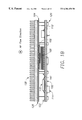
- FIG. 1A illustrates an exploded view of assembly 100 .
- Assembly 100 comprises first printed circuit board (PCB) 102 , second PCB 104 , and heat transfer device 106 .
- First PCB 102 can be a single layer PCB or multi-layer PCB, where the multi-layer PCB is comprised of alternating layers of conducting and non-conducting materials to allow electrical signals to be routed from device to device on the first PCB 102 .
- Devices 108 - 116 are shown mounted on first PCB 102 .
- Devices 114 and 116 are shown as being mounted on the opposite side of first PCB 102 as devices 108 - 112 . This illustrates that first PCB 102 can have devices 108 - 116 mounted on both sides.
- Device 108 is coupled to first PCB 102 via a Ball Grid Array (BGA) 118 .
- BGA 118 provides electrical contacts between device 108 and first PCB 102 .
- Other methods of electrical coupling between device 108 and first PCB 102 are possible, e.g., wire bonding, solder connections, etc. Further, there can also be thermal coupling between device 108 and PCB 102 if desired.
- Heat transfer device 106 couples device 108 to second PCB 104 .
- Heat transfer device 106 is typically a thermally conductive material, e.g., thermal grease, thermal epoxy, or a commercially produced material such as THERMA-GAPTM. Heat transfer device 106 provides a thermal interface between device 108 and the second PCB 104 .
- Heat transfer device 106 is typically a mechanically compliant material to allow for minimal applied pressure to the device 108 such that device 108 is not subjected to additional stress through use of heat transfer device 108 .
- Spacers 141 and fasteners 142 provide for a precision alignment between boards 102 and 104 and the device 108 such that a controlled gap exists in which heat transfer device 106 can properly be accommodated without deleterious air gaps nor excessive pressure applied to device 108 . Additionally, the location of the spacers 141 adjacent to the device 108 reduce variations in spacing caused by bow and warpage of board 102 and, to some extent, board 104 .
- Devices 110 - 116 that are thermally active but do not require heat transfer device 106 to cool the devices 110 - 116 and are cooled by conduction through first PCB 102 , or through convection should air flow be available across first PCB 102 . Otherwise, additional devices 110 - 116 can be coupled to second PCB 104 through additional heat transfer devices 106 .
- the present invention is not limited to a single device 108 that is cooled through the use of heat transfer device 106 . Any number of devices 108 - 116 can be cooled through the use of single or multiple heat transfer devices 106 .
- Second PCB 104 is mechanicaly coupled to first PCB 102 through the use of fasteners 120 and standoffs 122 .
- Fasteners 120 are typically screws, but can be other types of fasteners such as rivets, hollow feedthroughs, connectors, or other fasteners.
- Standoffs 122 are typically unthreaded inserts with a height equal to the height of spacer 141 .
- the fasteners 120 and standoffs 122 are located at mechanically and/or electrically desirable locations on first PCB 102 . These locations are typically at the periphery of first PCB 102 , but can be anywhere on first PCB 102 .
- Second PCB 104 has areas 124 that are designed to facilitate the transfer of heat from device 108 , through heat transfer device 106 , to a heat sink.
- Areas 124 comprise plated through holes (PTHs) 126 , consisting of holes in board 104 with interior walls of plated copper or other high thermally conductive material.
- PTHs plated through holes
- the region within the hole may be filled with metal, liquid filled areas, or other thermal transfer devices or mechanisms to enhance thermal conduction between the material 106 and the heatsink 130 .
- Areas 124 can be designed to be the same size, a larger size, or a smaller size than the device 108 , depending on the heat dissipation requirements for device 108 and the size of second PCB 104 .
- PTHs 126 provide a means of reducing air pockets in material 106 and to provide a volume where excesses of material 106 may flow in the case of a reduced gap between device 108 and board 104 . Still another benefit of PTHs 126 can be to adjust the thermal conductivity of the paths of multiple devices 108 on a single first PCB 102 to the common “isothermal” heatsink 130 such that if the two devices 108 have differing heat flow then the conductivity in each thermal path can be adjusted such that the junction temperature of each device 108 will be the same. This can be beneficial in improving timing margins of digital devices.
- a thermal interface such as a plate 128 is coupled to second PCB 104 to equalize and transfer heat from device 108 , through heat transfer device 106 and second PCB 104 area 124 to heat sink 130 .
- heatsink 130 can be any device, e.g., a heat pipe, or a layer on second PCB 104 that acts as an isothermal conduction layer to properly remove the heat generated by device 108 .
- Thermal interface 128 can be electrically conductive, or non-electrically conductive, depending on the design for second PCB 104 .
- thermal interface 128 should be electrically non-conductive so as not to interfere with signals travelling between devices 108 - 116 that are mounted on second PCB 104 .
- Thermal interface 128 can be they epoxy or any other material which thermally and mechanically bonds second PCB 104 to heatsink 130 .
- FIG. 1B illustrates the assembly 100 as a completed assembly.
- the thermal coupling of device 108 , heat transfer device 106 , second PCB 104 in conjunction with PTHs 126 , thermal interface 128 , and heatsink 130 provide a thermal path for heat generated by device 108 to be dissipated by heatsink 130 . Further, airflow can be provided to further cool device 108 and devices 110 - 116 .
- heatsink 130 can be larger or smaller than the area of second PCB 104 .
- Heatsink 130 also acts as a mechanical stabilizer for assembly 100 , to provide additional mechanical stability for assemblies 100 that will experience more severe mechanical environments, e.g., vibration.
- FIG. 1C illustrates assembly 100 in an isometric view.
- Heatsink 130 is shown as smaller than second PCB 104 and thermal interface 128 to illustrate the flexibility of the design of the present invention. Airflow can again be provided to increase the heat dissipation capabilities of assembly 100 .
- FIG. 1D illustrates an embodiment of the assembly 100 comprising a heat pipe 160 .
- FIGS. 2A-2B illustrate the construction of an encapsulated circuit assembly using the present invention for multiple heat generating integrated circuit devices.
- FIG. 2A illustrates an exploded view of assembly 100 .
- Assembly 100 comprises first printed circuit board (PCB) 102 , second PCB 104 , and heat transfer device 106 .
- First PCB 102 can be a single layer PCB or multi-layer PCB, where the multi-layer PCB is comprised of alternating layers of conducting and non-conducting materials to allow electrical signals to be routed from device to device on the first PCB 102 .
- Devices 108 , 114 - 116 , and 132 are shown mounted on first PCB 102 .
- Devices 114 and 116 are shown as being mounted on the opposite side of first PCB 102 as devices 108 and 132 . This illustrates that first PCB 102 can have devices 108 , 114 - 116 , and 132 mounted on both sides.
- BGA Ball Grid Array
- Heat transfer device 106 couples device 108 to second PCB 104 .
- Heat transfer device 106 is typically a thermally conductive material, e.g., thermal grease, thermal epoxy, or a commercially produced material such as THERMA-GAPTM. Heat transfer device 106 provides a thermal interface between device 108 and the second PCB 104 .
- Heat transfer device 106 is typically a mechanically compliant material to allow for minimal applied pressure to the device 108 such that device 108 is not subjected to additional stress through use of heat transfer device 108 .
- Spacers 141 and fasteners 142 provide for a precision alignment between boards 102 and 104 and the device 108 such that a controlled gap exists in which heat transfer device 106 can properly be accommodated without deleterious air gaps nor excessive pressure applied to device 108 . Additionally, the location of the spacers 141 adjacent to the device 108 reduce variations in spacing caused by bow and warpage of board 102 and, to some extent, board 104 .
- Devices 114 - 116 that are thermal active but do not require heat transfer device 106 to cool the devices 114 - 116 are cooled by conduction through first PCB 102 , or through convection should air flow be available across first PCB 102 .
- Device 132 is another heat generating device similar to device 108 . However, all devices 108 and 132 that will require additional cooling through heat transfer device 106 , second PCB 104 , and heatsink 130 are not the same size and/or height. Therefore, each device 108 and 132 must be treated individually using the present invention to best provide heat dissipation for each device 108 and 132 . In FIG. 2A, device 132 is shown as having a height 134 smaller than height 136 of device 108 . There can be many devices 108 and 132 of varying heights mounted on first PCB 102 , all of which can be cooled by the assembly 100 of the present invention, through use of an additional thermal interface 138 and a thermal conductive spacer 140 .
- Thermal interface 138 provides a thermal path for device 132 that will allow heat generated by device 132 to be dissipated by heatsink 130 .
- Thermal interface 138 can be similar to heat transfer device 106 , but can also be a different thermal transfer material to provide a proper thermal dissipative path.
- thermal interface 138 need not be mechanically compliant so long as thermal interface 106 above it is. Thus, the use of a hardening thermal epoxy may be useful to hold spacer 140 in place during assembly.
- Spacer 140 is provided to increase height 134 to approximate height 136 . This allows device 108 and device 132 to contact heat transfer device 106 , which in turn contacts second PCB 104 and heatsink 130 to transfer heat from devices 108 and 132 to heatsink 130 . Spacer 140 is shown as larger in size than device 132 , which can provide for heat spreading of the heat generated by device 132 to heatsink 130 . Spacer 140 can be of any size relative to device 132 . Further, there can be spacers 140 on more than one device 108 and 132 .
- Second PCB 104 is coupled mechanically to first PCB 102 through the use of fasteners 120 and standoffs 122 .
- Fasteners 120 are typically screws, but can be other types of fasteners such as rivets, feedthroughs that are hollow, connectors, or other fasteners.
- Standoffs 122 are typically unthreaded inserts with a height equal to the height of spacer 141 .
- the fasteners 120 and standoffs 122 are located at mechanically and/or electrically desirable locations on first PCB 102 . These locations are typically at the periphery of first PCB 102 , but can be anywhere on first PCB 102 .
- Second PCB 104 has areas 124 that are designed to facilitate the transfer of heat from devices 108 and 132 , through heat transfer device 106 , to a heat sink.
- Areas 124 comprise plated through holes (PTHs) 126 , consisting of holes in board 104 with interior was of plated copper or other high thermally conductive material.
- the region within the hole may be filled with metal, liquid filled areas, or other thermal transfer devices or mechanisms to enhance thermal conduction between material 106 and heatsink 130 .
- Areas 124 can be designed to be the same size, a larger size, or a smaller size than the device 108 , depending on the heat dissipation requirements for device 108 and the size of second PCB 104 .
- An additional benefit of PTHs 126 is to provide a means of reducing air pockets in material 106 and to provide a volume where excesses of material 106 may flow in the case of a reduced gap between device 108 and 104 .
- Thermal interface 128 is coupled to second PCB 104 to equalize and transfer heat from device 108 , through heat transfer device 106 and second PCB 104 area 124 to heat sink 130 .
- heatsink 130 can be any device, e.g., a heat pipe, or a layer on second PCB 104 that acts as an isothermal conduction layer to properly remove the heat generated by device 108 .
- Thermal interface 128 can be electrically conductive, or non-electrically conductive, depending on the design for second PCB 104 .
- thermal interface 128 can be electrically non-conductive so as not to interfere with signals travelling between devices 108 - 116 that are mounted on second PCB 104 .
- Thermal interface 128 can be thermal epoxy or any other material which thermally and mechanically bonds board 104 to heatsink 130 .
- FIG. 2B illustrates the assembly 100 of FIG. 2A as a completed assembly.
- the thermal coupling of devices 108 and 132 , heat transfer device 106 , thermal interface 138 , spacer 140 , second PCB 104 in conjunction with PTHs 126 , thermal interface 128 , and heatsink 130 provide thermal paths for heat generated by devices 108 and 132 to be dissipated by heatsink 130 . Further, airflow can be provided to further cool devices 108 and 132 , as well as devices 110 - 116 . Although shown as covering the entire area of second PCB 104 , heatsink 130 can be larger or smaller than the area of second PCB 104 . Heatsink 130 also acts as a mechanical stabilizer for assembly 100 , to provide additional mechanical stability for assemblies 100 that will experience more severe mechanical environments, e.g., vibration.
- FIG. 3A illustrates in plan and section views a molded plastic spacer 143 that may be used in place of spacers 141 around a device that must be thermally coupled to board 104 .
- This spacer has clearance holes 145 for fasteners 142 .
- spacer 143 is shown with four clearance holes 145 , spacer 143 can have any number of clearance holes 145 without departing from the scope of the present invention.
- Imbedded metal spacers may be molded into holes 145 where it may be desirous to provide electrical contact between board 102 and board 104 .
- Spacer 143 substantially surrounds device 108 , but can take any shape desired.
- spacer 143 A feature of the spacer is pins 144 that engage in mating holes of board 102 and act to hold spacer 143 in place until final assembly of assembly 100 .
- An additional benefit of spacer 143 is that it provides complete enclosure of device 108 to prevent accidental damage. Furthermore, spacer 143 may be used to provide thermal isolation between device 108 and the remainder of the board assembly 100 .
- FIG. 3B illustrates a molded plastic spacer 147 that may be used in place of spacers 141 which have been previously described as used to couple second PCB 104 to first PCB 102 .
- This spacer 147 is shown as having ten clearance holes 150 for fasteners 120 , however a larger or smaller number of fasteners may be used as the need and size of the PCBs 102 and 104 require.
- Imbedded metal spacers may be molded into holes 150 where it may be desirous to provide electrical contact between board 102 and board 104 .
- the entire molded assembly may be formed as a cast metal structure or other metallic form which may be useful in the containment of electromagnetic radiation.
- spacer 147 A feature of the spacer 147 is pins 149 that engage in mating holes of board 102 and act to hold in place spacer 147 until final assembly of 100 .
- An additional benefit of spacer 147 is that it provides complete enclosure of device 108 to prevent accidental damage.
- spacer 147 may be used to provide environmental isolation to the internal components of assembly 100 .
- FIGS. 4A-4C illustrate the construction of a printed circuit board using the present invention.
- FIG. 4A illustrates an exploded view of assembly 100 .
- Assembly 100 comprises first printed circuit board (PCB) 102 , second PCB 104 , and heat transfer device 106 .
- First PCB 102 can be a single layer PCB or multi-layer PCB, where the multi -layer PCB is comprised of alternating layers of conducting and non-conducting materials to allow electrical signals to be routed from device to device on the first PCB 102 .
- Devices 108 , 114 , and 116 are shown mounted on first PCB 102 .
- Devices 114 and 116 are shown as being mounted on the opposite side of first PCB 102 as device 108 . This illustrates that first PCB 102 can have devices 108 , 114 , and 116 mounted on both sides.
- Device 108 is coupled to first PCB 102 via a Ball Grid Array (BGA) 118 .
- BGA 118 provides electrical contacts between device 108 and first PCB 102 .
- Other methods of electrical coupling between device 108 and first PCB 102 are possible, e.g., wire bonding, solder connections, etc. Further, there can also be thermal coupling between device 108 and PCB 102 if desired.
- Heat transfer device 106 couples device 108 to second PCB 104 .
- Heat transfer device 106 is typically a thermally conductive material, e.g., thermal grease, thermal epoxy, or a commercially produced material such as THERMA-GAPTM. Heat transfer device 106 provides a thermal interface between device 108 and the second PCB 104 .
- Heat transfer device 106 is typically a mechanically compliant material to allow for minimal applied pressure to the device 108 such that device 108 is not subjected to additional stress through use of heat transfer device 108 .
- Spacers 141 and fasteners 142 provide for a precision alignment between boards 102 and 104 and the device 108 such that a controlled gap exists in which heat transfer device 106 can properly be accomnodated without deleterious air gaps nor excessive pressure applied to device 108 . Additionally, the location of the spacers 141 adjacent to the device 108 reduce variations in spacing caused by bow and warpage of board 102 and, to some extent, board 104 .
- Devices 114 - 116 that are thermally active but do not require heat transfer device 106 to cool the devices 114 - 116 are cooled by conduction through first PCB 102 , or through convection should air flow be available across first PCB 102 . Otherwise, additional devices 114 - 116 can be coupled to second PCB 104 through additional heat transfer devices 106 .
- the present invention is not limited to a single device 108 that is cooled through the use of heat transfer device 106 . Any number of devices 108 can be cooled through the use of single or multiple heat transfer devices 106 .
- Second PCB 104 is coupled mechanical to first PCB 102 through the use of fasteners 120 and standoffs 122 .
- Fasteners 120 are typically screws, but can be other types of fasteners such as rivets, hollow feedthroughs, connectors, or other fasteners.
- Standoffs 122 are typically unthreaded inserts with a height equal to the height of spacer 141 .
- the fasteners 120 and standoffs 122 are located at mechanically and/or electrically desirable locations on first PCB 102 . These locations are typically at the periphery of first PCB 102 , but can be anywhere on first PCB 102 .
- Second PCB 104 has areas 124 that are designed to facilitate the transfer of heat from device 108 , through heat transfer device 106 , to a heat sink.
- Areas 124 comprise plated though holes (PTHs) 126 , consisting of holes in board 104 with interior walls of plated copper or other high thermal conductive material.
- PTHs plated though holes
- the region within the hole may be filled with metal or other thermal transfer devices or mechanisms to enhance thermal conduction between the material 106 and the heatsink 130 .
- Areas 124 can be designed to be the same size, a larger size, or a smaller size than the device 108 , depending on the heat dissipation requirements for device 108 and the size of second PCB 104 .
- PTHs 126 provide a means of reducing air pockets in material 106 and to provide a volume where excesses of material 106 may flow in the case of a reduced gap between device 108 and board 104 . Still another benefit of PTHs 126 can be to adjust the thermal conductivity of the paths of devices 108 and 132 to the common “isothermal” lateral heat spreader block 146 such that if the two devices have differing heat flow then the conductivity in each path can be adjusted such that the junction temperature of each device will be the same. This can be beneficial in improving timing margins of digital devices.
- Thermal interface 128 is coupled to second PCB 104 to equalize and transfer heat from device 108 , through heat transfer device 106 and second PCB 104 area 124 to lateral heat spreader block 146 .
- Heat spreader block 146 is desirably of a thermally high conductivity material such as aluminum which allows the heat emanating from devices 108 and 132 to flow to heat sink 130 which is located outside of the volume used by boards 102 and 104 . Additionally, heat spreader block 146 may incorporate imbedded heat pipes to enhance lateral thermal conduction and/or reduce height. Although shown as a finned heat sink, heatsink 130 can be any device, e.g., a heat pipe, that can conduct heat out of the heat spreader block 146 .
- Thermal interface 128 can be electrically conductive, or non-electrically conductive, depending on the design for second PCB 104 . For example, if devices 108 - 116 need to be mounted on second PCB 104 , thermal interface 128 should be electrically non-conductive so as not to interfere with signals travelling between devices 108 - 116 that are mounted on second PCB 104 . Thermal interface 128 can be thermal epoxy or any other material which thermally and mechanically bonds board 104 to heatsink 130 and between heatsink 130 and heat spreader block 146 .
- heatsink 130 is now shown as being mounted outboard the volume occupied by PCB 102 and second PCB 104 .
- This flexibility of the present invention to mount the heatsink 130 at multiple locations provides additional design capabilities, i.e., the height of assembly 100 is now independent of the height of heatsink 130 .
- heat dissipative capability is provided without additional volume requirements for assembly 100 other than the height of heat spreader block 146 .
- FIG. 4B illustrates the assembly 100 as a completed assembly.
- the thermal coupling of device 108 , heat transfer device 106 , second PCB 104 , thermal interface 128 , heat spreader block 146 and heatsink 130 provide a thermal path for heat generated by device 108 to be dissipated by heatsink 130 . Further, airflow can be provided to further cool device 108 and devices 114 - 116 .
- Heatsink 130 can be larger or smaller than the height of PCB 102 , PCB 104 and heat spreader block 146 .
- Heat spreader block 146 also acts as a mechanical stabilizer for assembly 100 , to provide additional mechanical stability for assemblies 100 that will experience more severe mechanical environments, e.g., vibration.
- FIG. 4C illustrates assembly 100 in an isometric view.
- Heatsink 130 is shown as residing outboard of first PCB 102 and second PCB 104 .
- Thermal interface 128 is shown on the opposite side of second PCB 104 , and is shown as smaller than second PCB 104 to illustrate the flexibility of the design of the present invention. Airflow can again be provided to increase the heat dissipation capabilities of assembly 100 .
- FIGS. 4A-4C can be used where assembly 100 height is at a premium, or, where the heatsink 130 would be more efficient located outboard first PCB 102 and second PCB 104 than it would be if heatsink 130 sat atop second PCB 104 . This might occur when it is desirous to locate assembly 100 adjacent to similar assemblies 100 as close as practical to minimize electrical interconnect lengths, where airflow over the top of second PCB 104 is less than airflow outboard of assembly 100 . Further, the placement of heatsink 130 outboard first PCB 102 and second PCB 104 allows heatsink 130 to be electrically grounded, or placed at a desired potential, using both first PCB 102 and second PCB 104 .
- FIGS. 5A and 5B illustrate the thermal considerations of a printed circuit board embodying the present invention.
- FIG. 5A illustrates assembly 100 with the various thermal interfaces described for the present invention.
- the silicon die is represented as die 148 .
- Thermal Interface 1 (TI 1 ) 172 is the thermal interface internal to the device 108 between device heatspreader 178 and silicon die 148 . Heatspreader 178 may not always be present in which case thermal interface 172 would be used to represent the thermal resistance of the outside package surface to the silicon die 148 , e.g. molding compound.
- Thermal Interface 2 (TI 2 ) 174 is the interface between second PCB 104 and device 108 .
- Thermal Interface 3 (TI 3 ) 176 is the interface between second PCB 104 and heatsink 130 .
- Plated through holes (PTH) 180 is the area 124 of PCB 104 that allows thermal conduction through the board 104 .
- Heatsink (HSK) 130 is the device that couples the heat flow to the air or in some cases to thermal pipes to remote radiators.
- FIG. 5B illustrates the thermal schematic for the assembly 100 shown in FIG. 5 A.
- TI 1 172 receives a thermal resistance value
- HS 1 178 receives a thermal resistance value theta HS 1 ( ⁇ HS1 ) 188
- TI 2 174 receives a thermal resistance value
- HV 180 receives a thermal resistance value
- TI 3 176 receives a thermal resistance value
- HSK 130 receives a thermal resistance value, theta HSK ( ⁇ HSK ) 202 .
- a 1° C./W total thermal resistance for a 50 Watt device would yield a total temperature change of 50° C.
- FIG. 6 illustrates a flow chart describing the steps used in practicing the present invention.
- Block 204 represents the step of mounting a heat generating device on a first printed circuit board.
- Block 206 represents the step of thermal coupling the heat generating device to a heatsink coupled to a second printed circuit board, wherein a thermal path passes through the second printed circuit board.
- Assembly 100 can have both rigid and flexible layers to accommodate the needs of PCB designers without departing from the scope of the present invention. Further, the thicknesses of assembly 100 can be modified to accommodate components as needed.
- the present invention can also be used to shield device 108 from outside radiative effects, e.g., radiation, electromagnetic interference, etc. Further, device 108 can be shielded from emitting radiation and/or electromagnetic signals to the outside world through the use of the present invention.
- the present invention can also be used to provide power to devices through the second PCB 104 by contacting the device 108 through spacers 124 or standoffs 122 .
- the present invention discloses an encapuslated circuit assembly and a method for making such an assembly.
- the assembly comprises a first printed circuit board, a second printed circuit board, and a heat transfer device.
- the second printed circuit board comprises a heatsink, and the heat transfer device couples between a device mounted on the first printed circuit board and the second printed circuit board for transferring heat from the device to the heatsink of the second printed circuit board.
Abstract
Description

Claims (14)
Priority Applications (26)
| Application Number | Priority Date | Filing Date | Title |
|---|---|---|---|
| US09/353,428 US6304450B1 (en) | 1999-07-15 | 1999-07-15 | Inter-circuit encapsulated packaging |
| PCT/US2000/018081 WO2001006821A1 (en) | 1999-07-15 | 2000-06-28 | Encapsulated packaging in between 2 pcbs |
| AU59032/00A AU5903200A (en) | 1999-07-15 | 2000-06-28 | Encapsulated packaging in between 2 pcbs |
| US09/785,892 US6452113B2 (en) | 1999-07-15 | 2001-02-16 | Apparatus for providing power to a microprocessor with integrated thermal and EMI management |
| US09/798,541 US20010033476A1 (en) | 1999-07-15 | 2001-03-02 | Thermal/mechanical springbeam mechanism for heat transfer from heat source to heat dissipating device |
| US09/802,329 US6452804B1 (en) | 1999-07-15 | 2001-03-08 | Method and apparatus for thermal and mechanical management of a power regulator module and microprocessor in contact with a thermally conducting plate |
| US09/801,437 US6618268B2 (en) | 1999-07-15 | 2001-03-08 | Apparatus for delivering power to high performance electronic assemblies |
| US09/818,173 US20020008963A1 (en) | 1999-07-15 | 2001-03-26 | Inter-circuit encapsulated packaging |
| US09/885,780 US20010038527A1 (en) | 1999-07-15 | 2001-06-19 | Inter-circuit encapsulated packaging |
| US09/921,152 US6609914B2 (en) | 1999-07-15 | 2001-08-02 | High speed and density circular connector for board-to-board interconnection systems |
| US09/921,153 US6490160B2 (en) | 1999-07-15 | 2001-08-02 | Vapor chamber with integrated pin array |
| US10/022,454 US6556455B2 (en) | 1999-07-15 | 2001-10-30 | Ultra-low impedance power interconnection system for electronic packages |
| US10/005,024 US6741480B2 (en) | 1999-07-15 | 2001-12-04 | Integrated power delivery with flex circuit interconnection for high density power circuits for integrated circuits and systems |
| US10/036,957 US6847529B2 (en) | 1999-07-15 | 2001-12-20 | Ultra-low impedance power interconnection system for electronic packages |
| US10/132,586 US6623279B2 (en) | 1999-07-15 | 2002-04-25 | Separable power delivery connector |
| US10/147,395 US20020151195A1 (en) | 1999-07-15 | 2002-05-16 | Power interconnect method utilizing a flexible circuit between a voltage regulation module and an integrated circuit substrate |
| US10/147,138 US6947293B2 (en) | 1999-07-15 | 2002-05-16 | Method and apparatus for providing power to a microprocessor with integrated thermal and EMI management |
| US10/201,384 US7245507B2 (en) | 1999-07-15 | 2002-07-23 | Method and apparatus for providing power to a microprocessor with integrated thermal and EMI management |
| US10/245,908 US6754086B2 (en) | 1999-07-15 | 2002-09-17 | Integrated magnetic buck converter with magnetically coupled synchronously rectified mosfet gate drive |
| US10/290,722 US6801431B2 (en) | 1999-07-15 | 2002-11-08 | Integrated power delivery and cooling system for high power microprocessors |
| US10/385,387 US20030156400A1 (en) | 1999-07-15 | 2003-03-07 | Method and apparatus for providing power to a microprocessor with intergrated thermal and EMI management |
| US10/401,103 US20030214800A1 (en) | 1999-07-15 | 2003-03-25 | System and method for processor power delivery and thermal management |
| US11/197,034 US20050277310A1 (en) | 1999-07-15 | 2005-08-04 | System and method for processor power delivery and thermal management |
| US11/502,682 US7881072B2 (en) | 1999-07-15 | 2006-08-11 | System and method for processor power delivery and thermal management |
| US11/749,070 US20070268677A1 (en) | 1999-07-15 | 2007-05-15 | System and method for processor power delivery and thermal management |
| US12/827,732 US20100325882A1 (en) | 1999-07-15 | 2010-06-30 | System And Method For Processor Power Delivery And Thermal Management |
Applications Claiming Priority (1)
| Application Number | Priority Date | Filing Date | Title |
|---|---|---|---|
| US09/353,428 US6304450B1 (en) | 1999-07-15 | 1999-07-15 | Inter-circuit encapsulated packaging |
Related Child Applications (23)
| Application Number | Title | Priority Date | Filing Date |
|---|---|---|---|
| US09/432,872 Continuation-In-Part US6631426B1 (en) | 1999-11-02 | 1999-11-02 | Automatic ID allocation for AV/C entities |
| US09/432,878 Continuation-In-Part US6356448B1 (en) | 1999-07-15 | 1999-11-02 | Inter-circuit encapsulated packaging for power delivery |
| US72701600A Continuation-In-Part | 1999-07-15 | 2000-11-28 | |
| US09/785,892 Continuation-In-Part US6452113B2 (en) | 1999-07-15 | 2001-02-16 | Apparatus for providing power to a microprocessor with integrated thermal and EMI management |
| US09/798,541 Continuation-In-Part US20010033476A1 (en) | 1999-07-15 | 2001-03-02 | Thermal/mechanical springbeam mechanism for heat transfer from heat source to heat dissipating device |
| US09/801,437 Continuation-In-Part US6618268B2 (en) | 1999-07-15 | 2001-03-08 | Apparatus for delivering power to high performance electronic assemblies |
| US09/802,329 Continuation-In-Part US6452804B1 (en) | 1999-07-15 | 2001-03-08 | Method and apparatus for thermal and mechanical management of a power regulator module and microprocessor in contact with a thermally conducting plate |
| US09/818,173 Continuation-In-Part US20020008963A1 (en) | 1999-07-15 | 2001-03-26 | Inter-circuit encapsulated packaging |
| US09/885,780 Continuation US20010038527A1 (en) | 1999-07-15 | 2001-06-19 | Inter-circuit encapsulated packaging |
| US09/885,780 Continuation-In-Part US20010038527A1 (en) | 1999-07-15 | 2001-06-19 | Inter-circuit encapsulated packaging |
| US09/921,152 Continuation-In-Part US6609914B2 (en) | 1999-07-15 | 2001-08-02 | High speed and density circular connector for board-to-board interconnection systems |
| US09/921,153 Continuation-In-Part US6490160B2 (en) | 1999-07-15 | 2001-08-02 | Vapor chamber with integrated pin array |
| US10/022,454 Continuation US6556455B2 (en) | 1999-07-15 | 2001-10-30 | Ultra-low impedance power interconnection system for electronic packages |
| US10/005,024 Continuation-In-Part US6741480B2 (en) | 1999-07-15 | 2001-12-04 | Integrated power delivery with flex circuit interconnection for high density power circuits for integrated circuits and systems |
| US10/036,957 Continuation-In-Part US6847529B2 (en) | 1999-07-15 | 2001-12-20 | Ultra-low impedance power interconnection system for electronic packages |
| US10/132,586 Continuation-In-Part US6623279B2 (en) | 1999-07-15 | 2002-04-25 | Separable power delivery connector |
| US10/147,138 Continuation-In-Part US6947293B2 (en) | 1999-07-15 | 2002-05-16 | Method and apparatus for providing power to a microprocessor with integrated thermal and EMI management |
| US10/147,395 Continuation-In-Part US20020151195A1 (en) | 1999-07-15 | 2002-05-16 | Power interconnect method utilizing a flexible circuit between a voltage regulation module and an integrated circuit substrate |
| US10/201,384 Continuation US7245507B2 (en) | 1999-07-15 | 2002-07-23 | Method and apparatus for providing power to a microprocessor with integrated thermal and EMI management |
| US10/245,908 Continuation US6754086B2 (en) | 1999-07-15 | 2002-09-17 | Integrated magnetic buck converter with magnetically coupled synchronously rectified mosfet gate drive |
| US10/245,908 Continuation-In-Part US6754086B2 (en) | 1999-07-15 | 2002-09-17 | Integrated magnetic buck converter with magnetically coupled synchronously rectified mosfet gate drive |
| US10/290,722 Continuation US6801431B2 (en) | 1999-07-15 | 2002-11-08 | Integrated power delivery and cooling system for high power microprocessors |
| US10/290,722 Continuation-In-Part US6801431B2 (en) | 1999-07-15 | 2002-11-08 | Integrated power delivery and cooling system for high power microprocessors |
Publications (1)
| Publication Number | Publication Date |
|---|---|
| US6304450B1 true US6304450B1 (en) | 2001-10-16 |
Family
ID=23389061
Family Applications (2)
| Application Number | Title | Priority Date | Filing Date |
|---|---|---|---|
| US09/353,428 Expired - Fee Related US6304450B1 (en) | 1999-07-15 | 1999-07-15 | Inter-circuit encapsulated packaging |
| US09/885,780 Abandoned US20010038527A1 (en) | 1999-07-15 | 2001-06-19 | Inter-circuit encapsulated packaging |
Family Applications After (1)
| Application Number | Title | Priority Date | Filing Date |
|---|---|---|---|
| US09/885,780 Abandoned US20010038527A1 (en) | 1999-07-15 | 2001-06-19 | Inter-circuit encapsulated packaging |
Country Status (3)
| Country | Link |
|---|---|
| US (2) | US6304450B1 (en) |
| AU (1) | AU5903200A (en) |
| WO (1) | WO2001006821A1 (en) |
Cited By (137)
| Publication number | Priority date | Publication date | Assignee | Title |
|---|---|---|---|---|
| US6442033B1 (en) * | 1999-09-24 | 2002-08-27 | Virginia Tech Intellectual Properties, Inc. | Low-cost 3D flip-chip packaging technology for integrated power electronics modules |
| US20020172022A1 (en) * | 1999-07-15 | 2002-11-21 | Incep Technologies, Inc. | Method and apparatus for providing power to a microprocessor with integrated thermal and EMI management |
| US6490161B1 (en) * | 2002-01-08 | 2002-12-03 | International Business Machines Corporation | Peripheral land grid array package with improved thermal performance |
| US6535386B2 (en) * | 2000-12-05 | 2003-03-18 | Intel Corporation | Electronic assembly having a heat pipe that conducts heat from a semiconductor die |
| US20030057548A1 (en) * | 1999-07-15 | 2003-03-27 | Incep Technologies, Inc. | Integrated power delivery and cooling system for high power microprocessors |
| US20030080650A1 (en) * | 2001-10-31 | 2003-05-01 | Wong Marvin Glenn | Longitudinal piezoelectric optical latching relay |
| US6557675B2 (en) * | 2001-07-31 | 2003-05-06 | Compaq Information Technologies Group, L.P. | Tunable vibration damper for processor packages |
| US6594155B2 (en) * | 2001-03-21 | 2003-07-15 | Nec Corporation | Mounting structure of electronic parts |
| US6623279B2 (en) | 1999-07-15 | 2003-09-23 | Incep Technologies, Inc. | Separable power delivery connector |
| US20030184976A1 (en) * | 2002-04-02 | 2003-10-02 | Brandenburg Scott D. | Electromagnetic interference shield for overmolded packaging of an electronic assembly |
| US20030189773A1 (en) * | 2002-03-28 | 2003-10-09 | Wong Marvin Glenn | Piezoelectric optical relay |
| US6633213B1 (en) * | 2002-04-24 | 2003-10-14 | Agilent Technologies, Inc. | Double sided liquid metal micro switch |
| US20030194170A1 (en) * | 2002-04-10 | 2003-10-16 | Wong Marvin Glenn | Piezoelectric optical demultiplexing switch |
| US20030222282A1 (en) * | 2002-04-29 | 2003-12-04 | Fjelstad Joseph C. | Direct-connect signaling system |
| US20040066259A1 (en) * | 2002-10-08 | 2004-04-08 | Dove Lewis R. | Electrically isolated liquid metal micro-switches for integrally shielded microcircuits |
| US20040075162A1 (en) * | 2001-07-26 | 2004-04-22 | Ciena Corporation | Laser diode and heatsink quick connect/disconnect assembly |
| US6730866B1 (en) | 2003-04-14 | 2004-05-04 | Agilent Technologies, Inc. | High-frequency, liquid metal, latching relay array |
| US6740829B1 (en) | 2003-04-14 | 2004-05-25 | Agilent Technologies, Inc. | Insertion-type liquid metal latching relay |
| US6743990B1 (en) | 2002-12-12 | 2004-06-01 | Agilent Technologies, Inc. | Volume adjustment apparatus and method for use |
| US6747222B1 (en) | 2003-02-04 | 2004-06-08 | Agilent Technologies, Inc. | Feature formation in a nonphotoimagable material and switch incorporating same |
| US6750594B2 (en) | 2002-05-02 | 2004-06-15 | Agilent Technologies, Inc. | Piezoelectrically actuated liquid metal switch |
| US6750413B1 (en) | 2003-04-25 | 2004-06-15 | Agilent Technologies, Inc. | Liquid metal micro switches using patterned thick film dielectric as channels and a thin ceramic or glass cover plate |
| US20040112728A1 (en) * | 2002-12-12 | 2004-06-17 | Wong Marvin Glenn | Ceramic channel plate for a switch |
| US20040112726A1 (en) * | 2002-12-12 | 2004-06-17 | Wong Marvin Glenn | Ultrasonically milled channel plate for a switch |
| US20040112727A1 (en) * | 2002-12-12 | 2004-06-17 | Wong Marvin Glenn | Laser cut channel plate for a switch |
| US20040112729A1 (en) * | 2002-12-12 | 2004-06-17 | Wong Marvin Glenn | Switch and method for producing the same |
| US6756551B2 (en) | 2002-05-09 | 2004-06-29 | Agilent Technologies, Inc. | Piezoelectrically actuated liquid metal switch |
| US6759611B1 (en) | 2003-06-16 | 2004-07-06 | Agilent Technologies, Inc. | Fluid-based switches and methods for producing the same |
| US6759610B1 (en) | 2003-06-05 | 2004-07-06 | Agilent Technologies, Inc. | Multi-layer assembly of stacked LIMMS devices with liquid metal vias |
| US6762378B1 (en) | 2003-04-14 | 2004-07-13 | Agilent Technologies, Inc. | Liquid metal, latching relay with face contact |
| US6765161B1 (en) | 2003-04-14 | 2004-07-20 | Agilent Technologies, Inc. | Method and structure for a slug caterpillar piezoelectric latching reflective optical relay |
| US20040140187A1 (en) * | 2003-01-22 | 2004-07-22 | Wong Marvin Glenn | Method for registering a deposited material with channel plate channels, and switch produced using same |
| US6768068B1 (en) | 2003-04-14 | 2004-07-27 | Agilent Technologies, Inc. | Method and structure for a slug pusher-mode piezoelectrically actuated liquid metal switch |
| US20040144632A1 (en) * | 2003-01-13 | 2004-07-29 | Wong Marvin Glenn | Photoimaged channel plate for a switch |
| US20040148482A1 (en) * | 2003-01-13 | 2004-07-29 | Grundy Kevin P. | Memory chain |
| US6770827B1 (en) | 2003-04-14 | 2004-08-03 | Agilent Technologies, Inc. | Electrical isolation of fluid-based switches |
| US6774324B2 (en) | 2002-12-12 | 2004-08-10 | Agilent Technologies, Inc. | Switch and production thereof |
| US6774325B1 (en) | 2003-04-14 | 2004-08-10 | Agilent Technologies, Inc. | Reducing oxides on a switching fluid in a fluid-based switch |
| US6777630B1 (en) | 2003-04-30 | 2004-08-17 | Agilent Technologies, Inc. | Liquid metal micro switches using as channels and heater cavities matching patterned thick film dielectric layers on opposing thin ceramic plates |
| US6781074B1 (en) | 2003-07-30 | 2004-08-24 | Agilent Technologies, Inc. | Preventing corrosion degradation in a fluid-based switch |
| US6787720B1 (en) | 2003-07-31 | 2004-09-07 | Agilent Technologies, Inc. | Gettering agent and method to prevent corrosion in a fluid switch |
| US6794591B1 (en) | 2003-04-14 | 2004-09-21 | Agilent Technologies, Inc. | Fluid-based switches |
| US6798937B1 (en) | 2003-04-14 | 2004-09-28 | Agilent Technologies, Inc. | Pressure actuated solid slug optical latching relay |
| US20040188234A1 (en) * | 2003-03-31 | 2004-09-30 | Dove Lewis R. | Hermetic seal and controlled impedance rf connections for a liquid metal micro switch |
| US20040198076A1 (en) * | 2003-04-01 | 2004-10-07 | Kung-Fu Chen | Conversion module for liquid crystal display |
| US6803842B1 (en) | 2003-04-14 | 2004-10-12 | Agilent Technologies, Inc. | Longitudinal mode solid slug optical latching relay |
| US20040201309A1 (en) * | 2003-04-14 | 2004-10-14 | Wong Marvin Glenn | Insertion-type liquid metal latching relay array |
| US20040201315A1 (en) * | 2003-04-14 | 2004-10-14 | Wong Marvin Glenn | Bending-mode latching relay |
| US20040201311A1 (en) * | 2003-04-14 | 2004-10-14 | Wong Marvin Glenn | High frequency bending-mode latching relay |
| US20040202844A1 (en) * | 2003-04-14 | 2004-10-14 | Wong Marvin Glenn | Feature formation in thick-film inks |
| US20040201321A1 (en) * | 2003-04-14 | 2004-10-14 | Wong Marvin Glenn | High frequency latching relay with bending switch bar |
| US20040201312A1 (en) * | 2003-04-14 | 2004-10-14 | Arthur Fong | Method and structure for a slug assisted longitudinal piezoelectrically actuated liquid metal optical switch |
| US20040202413A1 (en) * | 2003-04-14 | 2004-10-14 | Wong Marvin Glenn | Method and structure for a solid slug caterpillar piezoelectric optical relay |
| US20040202558A1 (en) * | 2003-04-14 | 2004-10-14 | Arthur Fong | Closed-loop piezoelectric pump |
| US20040200705A1 (en) * | 2003-04-14 | 2004-10-14 | Wong Marvin Glenn | Formation of signal paths to increase maximum signal-carrying frequency of a fluid-based switch |
| US20040200704A1 (en) * | 2003-04-14 | 2004-10-14 | Arthur Fong | Fluid-based switch |
| US20040201319A1 (en) * | 2003-04-14 | 2004-10-14 | Wong Marvin Glenn | High frequency push-mode latching relay |
| US20040201440A1 (en) * | 2003-04-14 | 2004-10-14 | Arthur Fong | Longitudinal electromagnetic latching relay |
| US20040201322A1 (en) * | 2003-04-14 | 2004-10-14 | Wong Marvin Glenn | Longitudinal mode optical latching relay |
| US20040201313A1 (en) * | 2003-04-14 | 2004-10-14 | Wong Marvin Glenn | High-frequency, liquid metal, latching relay with face contact |
| US20040201329A1 (en) * | 2003-04-14 | 2004-10-14 | Wong Marvin Glenn | Damped longitudinal mode latching relay |
| US20040202410A1 (en) * | 2003-04-14 | 2004-10-14 | Wong Marvin Glenn | Longitudinal electromagnetic latching optical relay |
| US20040201310A1 (en) * | 2003-04-14 | 2004-10-14 | Wong Marvin Glenn | Damped longitudinal mode optical latching relay |
| US20040201320A1 (en) * | 2003-04-14 | 2004-10-14 | Carson Paul Thomas | Inserting-finger liquid metal relay |
| US20040201907A1 (en) * | 2003-04-14 | 2004-10-14 | Wong Marvin Glenn | Liquid metal optical relay |
| US20040201447A1 (en) * | 2003-04-14 | 2004-10-14 | Wong Marvin Glenn | Thin-film resistor device |
| US20040202414A1 (en) * | 2003-04-14 | 2004-10-14 | Wong Marvin Glenn | Reflecting wedge optical wavelength multiplexer/demultiplexer |
| US20040201330A1 (en) * | 2003-04-14 | 2004-10-14 | Arthur Fong | Method and apparatus for maintaining a liquid metal switch in a ready-to-switch condition |
| US20040200708A1 (en) * | 2003-04-14 | 2004-10-14 | Wong Marvin Glenn | Method and structure for a slug assisted pusher-mode piezoelectrically actuated liquid metal optical switch |
| US20040200707A1 (en) * | 2003-04-14 | 2004-10-14 | Wong Marvin Glenn | Bent switching fluid cavity |
| US20040200706A1 (en) * | 2003-04-14 | 2004-10-14 | Dove Lewis R. | Substrate with liquid electrode |
| US20040201316A1 (en) * | 2003-04-14 | 2004-10-14 | Arthur Fong | Method and structure for a solid slug caterpillar piezoelectric relay |
| US20040202411A1 (en) * | 2003-04-14 | 2004-10-14 | Wong Marvin Glenn | Method and structure for a pusher-mode piezoelectrically actuated liquid metal optical switch |
| US20040201317A1 (en) * | 2003-04-14 | 2004-10-14 | Wong Marvin Glenn | Method and structure for a pusher-mode piezoelectrically actuated liquid switch metal switch |
| US20040201314A1 (en) * | 2003-04-14 | 2004-10-14 | Wong Marvin Glenn | Wetting finger latching piezoelectric relay |
| US20040201323A1 (en) * | 2003-04-14 | 2004-10-14 | Wong Marvin Glenn | Shear mode liquid metal switch |
| US20040202408A1 (en) * | 2003-04-14 | 2004-10-14 | Wong Marvin Glenn | Pressure actuated optical latching relay |
| US20040202404A1 (en) * | 2003-04-14 | 2004-10-14 | Wong Marvin Glenn | Polymeric liquid metal optical switch |
| US20040200703A1 (en) * | 2003-04-14 | 2004-10-14 | Wong Marvin Glenn | Bending mode liquid metal switch |
| US20040200702A1 (en) * | 2003-04-14 | 2004-10-14 | Arthur Fong | Push-mode latching relay |
| US20040201318A1 (en) * | 2003-04-14 | 2004-10-14 | Wong Marvin Glen | Latching relay with switch bar |
| US20040212964A1 (en) * | 2003-04-28 | 2004-10-28 | Belady Christian L. | Stack up assembly |
| US20040236894A1 (en) * | 2003-04-10 | 2004-11-25 | Siliconpipe, Inc. | Memory system having a multiplexed high-speed channel |
| US6831838B1 (en) * | 2003-05-14 | 2004-12-14 | Illinois Tool Works Inc. | Circuit board assembly for welding power supply |
| US20040251117A1 (en) * | 2003-06-16 | 2004-12-16 | Wong Marvin Glenn | Suspended thin-film resistor |
| US20050014395A1 (en) * | 2003-01-13 | 2005-01-20 | Fjelstad Joseph C. | System for making high-speed connections to board-mounted modules |
| US20050034962A1 (en) * | 2003-04-14 | 2005-02-17 | Wong Marvin Glenn | Reducing oxides on a switching fluid in a fluid-based switch |
| US20050052687A1 (en) * | 2003-08-12 | 2005-03-10 | Murata Kikai Kabushiki Kaisha | Image processing device and communication terminal device |
| US6891272B1 (en) | 2002-07-31 | 2005-05-10 | Silicon Pipe, Inc. | Multi-path via interconnection structures and methods for manufacturing the same |
| US20050141195A1 (en) * | 2003-12-31 | 2005-06-30 | Himanshu Pokharna | Folded fin microchannel heat exchanger |
| US6927529B2 (en) | 2002-05-02 | 2005-08-09 | Agilent Technologies, Inc. | Solid slug longitudinal piezoelectric latching relay |
| US20050263379A1 (en) * | 2003-04-14 | 2005-12-01 | John Ralph Lindsey | Reduction of oxides in a fluid-based switch |
| US6979784B1 (en) | 2003-10-17 | 2005-12-27 | Advanced Micro Devices, Inc. | Component power interface board |
| US20060104034A1 (en) * | 2004-11-12 | 2006-05-18 | Via Technologies, Inc. | Heat-dissipating device |
| US20060109626A1 (en) * | 2004-11-24 | 2006-05-25 | Harris Shaun L | Multi-chip module with stacked redundant power |
| US20060109623A1 (en) * | 2004-11-24 | 2006-05-25 | Harris Shaun L | Apparatus and method for multiprocessor circuit board |
| US20060109625A1 (en) * | 2004-11-24 | 2006-05-25 | Harris Shaun L | Redundant power for processor circuit board |
| US20060126297A1 (en) * | 2004-12-13 | 2006-06-15 | Belady Christian L | Processor module with thermal dissipation device |
| US20060133041A1 (en) * | 2004-12-21 | 2006-06-22 | Belady Christian L | Processor module for system board |
| US20060139892A1 (en) * | 2003-01-29 | 2006-06-29 | Koninklijke Phillips Electronics N.V. | Heat dissipating arrangement for an electronic appliance |
| US20060181857A1 (en) * | 2005-02-16 | 2006-08-17 | Belady Christian L | Redundant power beneath circuit board |
| US20060187646A1 (en) * | 2005-02-18 | 2006-08-24 | Belson Steven A | Multi-processor module with redundant power |
| US20060192293A1 (en) * | 2005-02-25 | 2006-08-31 | Fujitsu Limited | Electronic device, standoff member, and method of manufacturing electronic device |
| US7131487B2 (en) * | 2001-12-14 | 2006-11-07 | Intel Corporation | Use of adjusted evaporator section area of heat pipe that is sized to match the surface area of an integrated heat spreader used in CPU packages in mobile computers |
| US20060273592A1 (en) * | 2005-06-06 | 2006-12-07 | Mitsubishi Denki Kabushiki Kaisha | Power unit |
| US20070188692A1 (en) * | 2004-03-16 | 2007-08-16 | Matsushita Electric Industrial Co., Ltd. | Driver module structure |
| US7269005B2 (en) | 2003-11-21 | 2007-09-11 | Intel Corporation | Pumped loop cooling with remote heat exchanger and display cooling |
| US20080037223A1 (en) * | 2006-08-12 | 2008-02-14 | Diehl Ako Stiftung & Co. Kg | Power Electronics with a Heat Sink |
| US20080068797A1 (en) * | 2006-09-15 | 2008-03-20 | Takashi Iikubo | Mounting assembly and electronic device with the mounting assembly |
| US7349225B1 (en) * | 2002-10-22 | 2008-03-25 | Odyssian Technology, Llc | Multifunctional composite sandwich element with embedded electronics |
| US20080130234A1 (en) * | 2006-11-30 | 2008-06-05 | Daisuke Maehara | Electronic Apparatus |
| US20080137307A1 (en) * | 2006-12-08 | 2008-06-12 | Chris Erwin Orr | Method and system for extracting heat from electrical components |
| US20080150125A1 (en) * | 2006-12-20 | 2008-06-26 | Henning Braunisch | Thermal management of dies on a secondary side of a package |
| US20090080163A1 (en) * | 2007-05-17 | 2009-03-26 | Lockheed Martin Corporation | Printed wiring board assembly |
| US20090096086A1 (en) * | 2007-10-15 | 2009-04-16 | Venkat Natarajan | Cooling system for semiconductor devices |
| US20090213552A1 (en) * | 2004-08-03 | 2009-08-27 | Infineon Technoligies Ag | Component arragement with an optimized assembly capability |
| US20090225522A1 (en) * | 2008-03-07 | 2009-09-10 | Panasonic Corporation | Electronic unit and electronic apparatus |
| US20090290321A1 (en) * | 2008-05-21 | 2009-11-26 | Hon Hai Precision Industry Co., Ltd. | Electrical connector having height-adjustable member |
| US20100020505A1 (en) * | 2008-07-28 | 2010-01-28 | Brodsky William L | Printed Circuit Board Assembly Having Multiple Land Grid Arrays for Providing Power Distribution |
| US7750446B2 (en) | 2002-04-29 | 2010-07-06 | Interconnect Portfolio Llc | IC package structures having separate circuit interconnection structures and assemblies constructed thereof |
| US20100320187A1 (en) * | 2009-06-17 | 2010-12-23 | Drs Test & Energy Management, Llc | Heat Sink and Thermal Plate Apparatus for Electronic Components |
| US7881072B2 (en) | 1999-07-15 | 2011-02-01 | Molex Incorporated | System and method for processor power delivery and thermal management |
| US20110205709A1 (en) * | 2010-02-24 | 2011-08-25 | Jian Yin | Sandwich structure with double-sided cooling and emi shielding |
| US20110292615A1 (en) * | 2010-05-28 | 2011-12-01 | Lear Corporation | Printed circuit board system for automotive power converter |
| WO2012002796A1 (en) * | 2010-06-28 | 2012-01-05 | Mimos Berhad | A heat sink and a method of enhancing heat dissipation thereof |
| US20120051008A1 (en) * | 2010-08-31 | 2012-03-01 | Cheng-Yu Wang | Circuit board with via hole and electronic device equipped with the same |
| US20130003310A1 (en) * | 2011-06-28 | 2013-01-03 | Oracle International Corporation | Chip package to support high-frequency processors |
| US20150109750A1 (en) * | 2011-03-11 | 2015-04-23 | Marvell Israel (M.I.S.L) Ltd. | Heat dissipating high power systems |
| CN104716112A (en) * | 2013-12-16 | 2015-06-17 | 英特尔公司 | Three-dimensional (3D) integrated heat spreader for multichip packages |
| US20160270261A1 (en) * | 2015-03-10 | 2016-09-15 | Kabushiki Kaisha Toshiba | Electronic apparatus |
| US10455685B1 (en) * | 2018-10-15 | 2019-10-22 | Intel Corporation | Electronic device, socket, and spacer to alter socket profile |
| CN111052363A (en) * | 2017-09-15 | 2020-04-21 | 莫列斯有限公司 | Grid array connector system |
| US11184979B2 (en) * | 2018-04-11 | 2021-11-23 | Phoenix Contact Gmbh & Co. Kg | Printed circuit board assembly |
| US11205867B2 (en) * | 2017-09-15 | 2021-12-21 | Molex, Llc | Grid array connector system |
| CN114510135A (en) * | 2022-02-16 | 2022-05-17 | 苏州生益兴热传科技有限公司 | Temperature-uniforming plate with good heat conduction and heat dissipation effects |
| US20240090115A1 (en) * | 2022-09-13 | 2024-03-14 | Hamilton Sundstrand Corporation | Circuit mounting assemblies |
| CN114510135B (en) * | 2022-02-16 | 2024-04-05 | 苏州生益兴热传科技有限公司 | Uniform temperature plate with good heat conduction and heat dissipation effects |
Families Citing this family (23)
| Publication number | Priority date | Publication date | Assignee | Title |
|---|---|---|---|---|
| US6452113B2 (en) | 1999-07-15 | 2002-09-17 | Incep Technologies, Inc. | Apparatus for providing power to a microprocessor with integrated thermal and EMI management |
| EP1256263A2 (en) * | 2000-02-18 | 2002-11-13 | Incep Technologies, Inc. | Method and apparatus for providing power to a microprocessor with integrated thermal and emi management |
| DE10107839A1 (en) | 2001-02-16 | 2002-09-05 | Philips Corp Intellectual Pty | Arrangement with an integrated circuit mounted on a carrier and a power supply assembly |
| US7286354B2 (en) | 2004-10-27 | 2007-10-23 | Brother Kogyo Kabushiki Kaisha | Electronic part-mounted substrate, thermal conductive member for electronic part-mounted substrate and liquid-jetting head |
| US20080055855A1 (en) * | 2006-09-06 | 2008-03-06 | Vinod Kamath | Heat sink for electronic components |
| US9019166B2 (en) | 2009-06-15 | 2015-04-28 | Raytheon Company | Active electronically scanned array (AESA) card |
| US7671696B1 (en) | 2006-09-21 | 2010-03-02 | Raytheon Company | Radio frequency interconnect circuits and techniques |
| US9172145B2 (en) | 2006-09-21 | 2015-10-27 | Raytheon Company | Transmit/receive daughter card with integral circulator |
| US8279131B2 (en) | 2006-09-21 | 2012-10-02 | Raytheon Company | Panel array |
| US8011950B2 (en) | 2009-02-18 | 2011-09-06 | Cinch Connectors, Inc. | Electrical connector |
| US8270169B2 (en) | 2009-03-24 | 2012-09-18 | Raytheon Company | Translating hinge |
| US8537552B2 (en) | 2009-09-25 | 2013-09-17 | Raytheon Company | Heat sink interface having three-dimensional tolerance compensation |
| US8508943B2 (en) | 2009-10-16 | 2013-08-13 | Raytheon Company | Cooling active circuits |
| US8363413B2 (en) | 2010-09-13 | 2013-01-29 | Raytheon Company | Assembly to provide thermal cooling |
| US8810448B1 (en) | 2010-11-18 | 2014-08-19 | Raytheon Company | Modular architecture for scalable phased array radars |
| US8355255B2 (en) | 2010-12-22 | 2013-01-15 | Raytheon Company | Cooling of coplanar active circuits |
| WO2014074045A1 (en) * | 2012-11-06 | 2014-05-15 | Telefonaktiebolaget L M Ericsson (Publ) | Heat dissipation assembly |
| US9407021B2 (en) | 2013-12-29 | 2016-08-02 | Continental Automotive Systems, Inc. | Compound cylinder PCB connection |
| US9942975B2 (en) | 2015-10-05 | 2018-04-10 | Raytheon Company | Scalable thermal solution for high frequency panel array applications or other applications |
| US20170285685A1 (en) * | 2016-04-04 | 2017-10-05 | Guy A. Mascaro | Heat Dissipating Structures and Mobility Apparatus for Electronic Headset Frames |
| KR102477829B1 (en) | 2019-04-12 | 2022-12-15 | 삼성전자 주식회사 | A converter including a printed circuit board and power converting module including the converter |
| CN113311647B (en) * | 2021-04-30 | 2023-02-28 | 北京空间机电研究所 | Camera system refrigeration loop structure |
| US20230067409A1 (en) * | 2021-08-31 | 2023-03-02 | Arista Networks, Inc. | Damper system for a lidless integrated circuit |
Citations (44)
| Publication number | Priority date | Publication date | Assignee | Title |
|---|---|---|---|---|
| US4498530A (en) | 1981-08-03 | 1985-02-12 | International Business Machines Corporation | Flexible thermal conduction element for cooling semiconductor devices |
| US4521829A (en) | 1982-09-09 | 1985-06-04 | Siemens Aktiengesellschaft | Device for cooling a plurality of integrated modules combined on a rigid printed circuitboard to form logic cards |
| US4589057A (en) | 1984-07-23 | 1986-05-13 | Rogers Corporation | Cooling and power and/or ground distribution system for integrated circuits |
| US4760495A (en) | 1987-04-16 | 1988-07-26 | Prime Computer Inc. | Stand-off device |
| US4771365A (en) | 1987-10-30 | 1988-09-13 | Honeywell Inc. | Passive cooled electronic chassis |
| US4942497A (en) | 1987-07-24 | 1990-07-17 | Nec Corporation | Cooling structure for heat generating electronic components mounted on a substrate |
| US5052481A (en) | 1988-05-26 | 1991-10-01 | International Business Machines Corporation | High conduction cooling module having internal fins and compliant interfaces for vlsi chip technology |
| US5161089A (en) | 1990-06-04 | 1992-11-03 | International Business Machines Corporation | Enhanced multichip module cooling with thermally optimized pistons and closely coupled convective cooling channels, and methods of manufacturing the same |
| US5195020A (en) | 1987-05-25 | 1993-03-16 | Fujitsu Limited | Cooling system used with an electronic circuit device for cooling circuit components included therein having a thermally conductive compound layer and method for forming the layer |
| US5272599A (en) * | 1993-03-19 | 1993-12-21 | Compaq Computer Corporation | Microprocessor heat dissipation apparatus for a printed circuit board |
| EP0582145A1 (en) | 1992-08-05 | 1994-02-09 | The Whitaker Corporation | Coaxial connector for connecting two circuit boards |
| US5331510A (en) * | 1991-08-30 | 1994-07-19 | Hitachi, Ltd. | Electronic equipment and computer with heat pipe |
| US5343358A (en) | 1993-04-26 | 1994-08-30 | Ncr Corporation | Apparatus for cooling electronic devices |
| US5365402A (en) | 1990-11-30 | 1994-11-15 | Hitachi, Ltd. | Cooling apparatus of electronic device |
| US5390078A (en) * | 1993-08-30 | 1995-02-14 | At&T Global Information Solutions Company | Apparatus for using an active circuit board as a heat sink |
| US5396403A (en) | 1993-07-06 | 1995-03-07 | Hewlett-Packard Company | Heat sink assembly with thermally-conductive plate for a plurality of integrated circuits on a substrate |
| US5409055A (en) | 1992-03-31 | 1995-04-25 | Furukawa Electric Co., Ltd. | Heat pipe type radiation for electronic apparatus |
| US5467251A (en) | 1993-10-08 | 1995-11-14 | Northern Telecom Limited | Printed circuit boards and heat sink structures |
| US5473510A (en) * | 1994-03-25 | 1995-12-05 | Convex Computer Corporation | Land grid array package/circuit board assemblies and methods for constructing the same |
| US5504924A (en) | 1990-11-28 | 1996-04-02 | Hitachi, Ltd. | Cooling system of electronic computer using flexible members in contact with semiconductor devices on boards |
| US5510958A (en) | 1994-01-11 | 1996-04-23 | Yokogawa Electric Corporation | Electronic circuit module having improved cooling arrangement |
| US5515912A (en) | 1990-03-02 | 1996-05-14 | Hitachi, Ltd. | Cooling apparatus of electronic devices |
| EP0717443A1 (en) | 1994-07-04 | 1996-06-19 | Matsushita Electric Industrial Co., Ltd. | Integrated circuit device |
| WO1996023397A1 (en) | 1995-01-25 | 1996-08-01 | Northern Telecom Limited | Printed circuit board and heat sink arrangement |
| US5619399A (en) * | 1995-02-16 | 1997-04-08 | Micromodule Systems, Inc. | Multiple chip module mounting assembly and computer using same |
| US5621615A (en) * | 1995-03-31 | 1997-04-15 | Hewlett-Packard Company | Low cost, high thermal performance package for flip chips with low mechanical stress on chip |
| US5646826A (en) | 1995-01-26 | 1997-07-08 | Northern Telecom Limited | Printed circuit board and heat sink arrangement |
| US5708566A (en) | 1996-10-31 | 1998-01-13 | Motorola, Inc. | Solder bonded electronic module |
| US5729433A (en) * | 1996-01-30 | 1998-03-17 | Micromodule Systems, Inc. | Multiple chip module assembly for top of mother board |
| US5734555A (en) * | 1994-03-30 | 1998-03-31 | Intel Corporation | Shared socket multi-chip module and/or piggyback pin grid array package |
| US5761043A (en) | 1996-02-22 | 1998-06-02 | Cray Research, Inc. | Daughter card assembly |
| US5796582A (en) | 1996-11-21 | 1998-08-18 | Northern Telecom Limited | Printed circuit board and heat sink arrangement |
| US5794454A (en) | 1996-12-04 | 1998-08-18 | International Business Machines Corporation | Cooling device for hard to access non-coplanar circuit chips |
| US5801924A (en) | 1996-02-22 | 1998-09-01 | Cray Research, Inc. | Method and apparatus for cooling daughter card modules |
| US5815921A (en) | 1994-01-26 | 1998-10-06 | Sun Microsystems, Inc. | Electronic package cooling system and heat sink with heat transfer assembly |
| US5825633A (en) | 1996-11-05 | 1998-10-20 | Motorola, Inc. | Multi-board electronic assembly including spacer for multiple electrical interconnections |
| US5842514A (en) | 1997-03-05 | 1998-12-01 | Northern Telecom Limited | Electronic unit |
| US5856911A (en) | 1996-11-12 | 1999-01-05 | National Semiconductor Corporation | Attachment assembly for integrated circuits |
| JPH1174427A (en) | 1997-09-01 | 1999-03-16 | Sharp Corp | Heat radiation structure of circuit element |
| US5898573A (en) | 1997-09-29 | 1999-04-27 | Ericsson Inc. | Microelectronic packages and packaging methods including thermally and electrically conductive pad |
| EP0920055A2 (en) | 1997-11-28 | 1999-06-02 | Robert Bosch Gmbh | Cooling device for a heat generating componant on a printed board |
| US5920458A (en) | 1997-05-28 | 1999-07-06 | Lucent Technologies Inc. | Enhanced cooling of a heat dissipating circuit element |
| US5930115A (en) * | 1996-08-26 | 1999-07-27 | Compaq Computer Corp. | Apparatus, method and system for thermal management of a semiconductor device |
| US5986887A (en) | 1998-10-28 | 1999-11-16 | Unisys Corporation | Stacked circuit board assembly adapted for heat dissipation |
-
1999
- 1999-07-15 US US09/353,428 patent/US6304450B1/en not_active Expired - Fee Related
-
2000
- 2000-06-28 AU AU59032/00A patent/AU5903200A/en not_active Abandoned
- 2000-06-28 WO PCT/US2000/018081 patent/WO2001006821A1/en active Application Filing
-
2001
- 2001-06-19 US US09/885,780 patent/US20010038527A1/en not_active Abandoned
Patent Citations (46)
| Publication number | Priority date | Publication date | Assignee | Title |
|---|---|---|---|---|
| US4498530A (en) | 1981-08-03 | 1985-02-12 | International Business Machines Corporation | Flexible thermal conduction element for cooling semiconductor devices |
| US4521829A (en) | 1982-09-09 | 1985-06-04 | Siemens Aktiengesellschaft | Device for cooling a plurality of integrated modules combined on a rigid printed circuitboard to form logic cards |
| US4589057A (en) | 1984-07-23 | 1986-05-13 | Rogers Corporation | Cooling and power and/or ground distribution system for integrated circuits |
| US4760495A (en) | 1987-04-16 | 1988-07-26 | Prime Computer Inc. | Stand-off device |
| US5195020A (en) | 1987-05-25 | 1993-03-16 | Fujitsu Limited | Cooling system used with an electronic circuit device for cooling circuit components included therein having a thermally conductive compound layer and method for forming the layer |
| US4942497A (en) | 1987-07-24 | 1990-07-17 | Nec Corporation | Cooling structure for heat generating electronic components mounted on a substrate |
| US4771365A (en) | 1987-10-30 | 1988-09-13 | Honeywell Inc. | Passive cooled electronic chassis |
| US5052481A (en) | 1988-05-26 | 1991-10-01 | International Business Machines Corporation | High conduction cooling module having internal fins and compliant interfaces for vlsi chip technology |
| US5515912A (en) | 1990-03-02 | 1996-05-14 | Hitachi, Ltd. | Cooling apparatus of electronic devices |
| US5161089A (en) | 1990-06-04 | 1992-11-03 | International Business Machines Corporation | Enhanced multichip module cooling with thermally optimized pistons and closely coupled convective cooling channels, and methods of manufacturing the same |
| US5504924A (en) | 1990-11-28 | 1996-04-02 | Hitachi, Ltd. | Cooling system of electronic computer using flexible members in contact with semiconductor devices on boards |
| US5365402A (en) | 1990-11-30 | 1994-11-15 | Hitachi, Ltd. | Cooling apparatus of electronic device |
| US5331510A (en) * | 1991-08-30 | 1994-07-19 | Hitachi, Ltd. | Electronic equipment and computer with heat pipe |
| US5409055A (en) | 1992-03-31 | 1995-04-25 | Furukawa Electric Co., Ltd. | Heat pipe type radiation for electronic apparatus |
| EP0582145A1 (en) | 1992-08-05 | 1994-02-09 | The Whitaker Corporation | Coaxial connector for connecting two circuit boards |
| US5272599A (en) * | 1993-03-19 | 1993-12-21 | Compaq Computer Corporation | Microprocessor heat dissipation apparatus for a printed circuit board |
| US5343358A (en) | 1993-04-26 | 1994-08-30 | Ncr Corporation | Apparatus for cooling electronic devices |
| US5396403A (en) | 1993-07-06 | 1995-03-07 | Hewlett-Packard Company | Heat sink assembly with thermally-conductive plate for a plurality of integrated circuits on a substrate |
| US5390078A (en) * | 1993-08-30 | 1995-02-14 | At&T Global Information Solutions Company | Apparatus for using an active circuit board as a heat sink |
| US5467251A (en) | 1993-10-08 | 1995-11-14 | Northern Telecom Limited | Printed circuit boards and heat sink structures |
| US5661902A (en) | 1993-10-08 | 1997-09-02 | Northern Telecom Limited | Methods of making printed circuit boards and heat sink structures |
| US5510958A (en) | 1994-01-11 | 1996-04-23 | Yokogawa Electric Corporation | Electronic circuit module having improved cooling arrangement |
| US5815921A (en) | 1994-01-26 | 1998-10-06 | Sun Microsystems, Inc. | Electronic package cooling system and heat sink with heat transfer assembly |
| US5473510A (en) * | 1994-03-25 | 1995-12-05 | Convex Computer Corporation | Land grid array package/circuit board assemblies and methods for constructing the same |
| US5734555A (en) * | 1994-03-30 | 1998-03-31 | Intel Corporation | Shared socket multi-chip module and/or piggyback pin grid array package |
| EP0717443A1 (en) | 1994-07-04 | 1996-06-19 | Matsushita Electric Industrial Co., Ltd. | Integrated circuit device |
| WO1996023397A1 (en) | 1995-01-25 | 1996-08-01 | Northern Telecom Limited | Printed circuit board and heat sink arrangement |
| US5646826A (en) | 1995-01-26 | 1997-07-08 | Northern Telecom Limited | Printed circuit board and heat sink arrangement |
| US5619399A (en) * | 1995-02-16 | 1997-04-08 | Micromodule Systems, Inc. | Multiple chip module mounting assembly and computer using same |
| US5621615A (en) * | 1995-03-31 | 1997-04-15 | Hewlett-Packard Company | Low cost, high thermal performance package for flip chips with low mechanical stress on chip |
| US5729433A (en) * | 1996-01-30 | 1998-03-17 | Micromodule Systems, Inc. | Multiple chip module assembly for top of mother board |
| US5761043A (en) | 1996-02-22 | 1998-06-02 | Cray Research, Inc. | Daughter card assembly |
| US5801924A (en) | 1996-02-22 | 1998-09-01 | Cray Research, Inc. | Method and apparatus for cooling daughter card modules |
| US5930115A (en) * | 1996-08-26 | 1999-07-27 | Compaq Computer Corp. | Apparatus, method and system for thermal management of a semiconductor device |
| US5708566A (en) | 1996-10-31 | 1998-01-13 | Motorola, Inc. | Solder bonded electronic module |
| US5825633A (en) | 1996-11-05 | 1998-10-20 | Motorola, Inc. | Multi-board electronic assembly including spacer for multiple electrical interconnections |
| US5856911A (en) | 1996-11-12 | 1999-01-05 | National Semiconductor Corporation | Attachment assembly for integrated circuits |
| US5796582A (en) | 1996-11-21 | 1998-08-18 | Northern Telecom Limited | Printed circuit board and heat sink arrangement |
| US5794454A (en) | 1996-12-04 | 1998-08-18 | International Business Machines Corporation | Cooling device for hard to access non-coplanar circuit chips |
| US5842514A (en) | 1997-03-05 | 1998-12-01 | Northern Telecom Limited | Electronic unit |
| US5920458A (en) | 1997-05-28 | 1999-07-06 | Lucent Technologies Inc. | Enhanced cooling of a heat dissipating circuit element |
| JPH1174427A (en) | 1997-09-01 | 1999-03-16 | Sharp Corp | Heat radiation structure of circuit element |
| US5995370A (en) | 1997-09-01 | 1999-11-30 | Sharp Kabushiki Kaisha | Heat-sinking arrangement for circuit elements |
| US5898573A (en) | 1997-09-29 | 1999-04-27 | Ericsson Inc. | Microelectronic packages and packaging methods including thermally and electrically conductive pad |
| EP0920055A2 (en) | 1997-11-28 | 1999-06-02 | Robert Bosch Gmbh | Cooling device for a heat generating componant on a printed board |
| US5986887A (en) | 1998-10-28 | 1999-11-16 | Unisys Corporation | Stacked circuit board assembly adapted for heat dissipation |
Cited By (237)
| Publication number | Priority date | Publication date | Assignee | Title |
|---|---|---|---|---|
| US7881072B2 (en) | 1999-07-15 | 2011-02-01 | Molex Incorporated | System and method for processor power delivery and thermal management |
| US20030057548A1 (en) * | 1999-07-15 | 2003-03-27 | Incep Technologies, Inc. | Integrated power delivery and cooling system for high power microprocessors |
| US20020172022A1 (en) * | 1999-07-15 | 2002-11-21 | Incep Technologies, Inc. | Method and apparatus for providing power to a microprocessor with integrated thermal and EMI management |
| US6801431B2 (en) * | 1999-07-15 | 2004-10-05 | Incep Technologies, Inc. | Integrated power delivery and cooling system for high power microprocessors |
| US6623279B2 (en) | 1999-07-15 | 2003-09-23 | Incep Technologies, Inc. | Separable power delivery connector |
| US6442033B1 (en) * | 1999-09-24 | 2002-08-27 | Virginia Tech Intellectual Properties, Inc. | Low-cost 3D flip-chip packaging technology for integrated power electronics modules |
| US6535386B2 (en) * | 2000-12-05 | 2003-03-18 | Intel Corporation | Electronic assembly having a heat pipe that conducts heat from a semiconductor die |
| US6594155B2 (en) * | 2001-03-21 | 2003-07-15 | Nec Corporation | Mounting structure of electronic parts |
| US7018870B2 (en) | 2001-07-26 | 2006-03-28 | Ciena Corporation | Laser diode and heatsink quick connect/disconnect assembly |
| US20040075162A1 (en) * | 2001-07-26 | 2004-04-22 | Ciena Corporation | Laser diode and heatsink quick connect/disconnect assembly |
| US6730993B1 (en) * | 2001-07-26 | 2004-05-04 | Ciena Corporation | Laser diode and heatsink quick connect/disconnect assembly |
| US6557675B2 (en) * | 2001-07-31 | 2003-05-06 | Compaq Information Technologies Group, L.P. | Tunable vibration damper for processor packages |
| US20030080650A1 (en) * | 2001-10-31 | 2003-05-01 | Wong Marvin Glenn | Longitudinal piezoelectric optical latching relay |
| US7078849B2 (en) | 2001-10-31 | 2006-07-18 | Agilent Technologies, Inc. | Longitudinal piezoelectric optical latching relay |
| US7131487B2 (en) * | 2001-12-14 | 2006-11-07 | Intel Corporation | Use of adjusted evaporator section area of heat pipe that is sized to match the surface area of an integrated heat spreader used in CPU packages in mobile computers |
| US6490161B1 (en) * | 2002-01-08 | 2002-12-03 | International Business Machines Corporation | Peripheral land grid array package with improved thermal performance |
| US20030189773A1 (en) * | 2002-03-28 | 2003-10-09 | Wong Marvin Glenn | Piezoelectric optical relay |
| US6741767B2 (en) | 2002-03-28 | 2004-05-25 | Agilent Technologies, Inc. | Piezoelectric optical relay |
| US6807731B2 (en) * | 2002-04-02 | 2004-10-26 | Delphi Technologies, Inc. | Method for forming an electronic assembly |
| US20030184976A1 (en) * | 2002-04-02 | 2003-10-02 | Brandenburg Scott D. | Electromagnetic interference shield for overmolded packaging of an electronic assembly |
| US20050081377A1 (en) * | 2002-04-02 | 2005-04-21 | Delphi Technologies, Inc. | Method for forming an electronic assembly |
| US20030194170A1 (en) * | 2002-04-10 | 2003-10-16 | Wong Marvin Glenn | Piezoelectric optical demultiplexing switch |
| US6633213B1 (en) * | 2002-04-24 | 2003-10-14 | Agilent Technologies, Inc. | Double sided liquid metal micro switch |
| US20030222282A1 (en) * | 2002-04-29 | 2003-12-04 | Fjelstad Joseph C. | Direct-connect signaling system |
| US7750446B2 (en) | 2002-04-29 | 2010-07-06 | Interconnect Portfolio Llc | IC package structures having separate circuit interconnection structures and assemblies constructed thereof |
| US7307293B2 (en) | 2002-04-29 | 2007-12-11 | Silicon Pipe, Inc. | Direct-connect integrated circuit signaling system for bypassing intra-substrate printed circuit signal paths |
| WO2003094203A3 (en) * | 2002-04-29 | 2004-01-08 | Silicon Pipe Inc | Direct-connect signaling system |
| US7989929B2 (en) | 2002-04-29 | 2011-08-02 | Samsung Electronics Co., Ltd. | Direct-connect signaling system |
| US6750594B2 (en) | 2002-05-02 | 2004-06-15 | Agilent Technologies, Inc. | Piezoelectrically actuated liquid metal switch |
| US6927529B2 (en) | 2002-05-02 | 2005-08-09 | Agilent Technologies, Inc. | Solid slug longitudinal piezoelectric latching relay |
| US6756551B2 (en) | 2002-05-09 | 2004-06-29 | Agilent Technologies, Inc. | Piezoelectrically actuated liquid metal switch |
| US6891272B1 (en) | 2002-07-31 | 2005-05-10 | Silicon Pipe, Inc. | Multi-path via interconnection structures and methods for manufacturing the same |
| US6781075B2 (en) | 2002-10-08 | 2004-08-24 | Agilent Technologies, Inc. | Electrically isolated liquid metal micro-switches for integrally shielded microcircuits |
| US20040066259A1 (en) * | 2002-10-08 | 2004-04-08 | Dove Lewis R. | Electrically isolated liquid metal micro-switches for integrally shielded microcircuits |
| US7349225B1 (en) * | 2002-10-22 | 2008-03-25 | Odyssian Technology, Llc | Multifunctional composite sandwich element with embedded electronics |
| US6924444B2 (en) | 2002-12-12 | 2005-08-02 | Agilent Technologies, Inc. | Ceramic channel plate for a fluid-based switch, and method for making same |
| US20040112728A1 (en) * | 2002-12-12 | 2004-06-17 | Wong Marvin Glenn | Ceramic channel plate for a switch |
| US20050000620A1 (en) * | 2002-12-12 | 2005-01-06 | Wong Marvin Glenn | Method for making switch with ultrasonically milled channel plate |
| US20050000784A1 (en) * | 2002-12-12 | 2005-01-06 | Wong Marvin Glenn | Liquid switch production and assembly |
| US6849144B2 (en) | 2002-12-12 | 2005-02-01 | Agilent Technologies, Inc. | Method for making switch with ultrasonically milled channel plate |
| US6774324B2 (en) | 2002-12-12 | 2004-08-10 | Agilent Technologies, Inc. | Switch and production thereof |
| US6855898B2 (en) | 2002-12-12 | 2005-02-15 | Agilent Technologies, Inc. | Ceramic channel plate for a switch |
| US20050051412A1 (en) * | 2002-12-12 | 2005-03-10 | Wong Marvin Glenn | Ceramic channel plate for a fluid-based switch, and method for making same |
| US6743990B1 (en) | 2002-12-12 | 2004-06-01 | Agilent Technologies, Inc. | Volume adjustment apparatus and method for use |
| US20040112729A1 (en) * | 2002-12-12 | 2004-06-17 | Wong Marvin Glenn | Switch and method for producing the same |
| US20040112724A1 (en) * | 2002-12-12 | 2004-06-17 | Wong Marvin Glenn | Volume adjustment apparatus and method for use |
| US6909059B2 (en) | 2002-12-12 | 2005-06-21 | Agilent Technologies, Inc. | Liquid switch production and assembly |
| US7022926B2 (en) | 2002-12-12 | 2006-04-04 | Agilent Technologies, Inc. | Ultrasonically milled channel plate for a switch |
| US20040112726A1 (en) * | 2002-12-12 | 2004-06-17 | Wong Marvin Glenn | Ultrasonically milled channel plate for a switch |
| US20040112727A1 (en) * | 2002-12-12 | 2004-06-17 | Wong Marvin Glenn | Laser cut channel plate for a switch |
| US8244993B2 (en) | 2003-01-13 | 2012-08-14 | Samsung Electronics Co., Ltd. | Memory chain |
| US20040144632A1 (en) * | 2003-01-13 | 2004-07-29 | Wong Marvin Glenn | Photoimaged channel plate for a switch |
| US7019235B2 (en) | 2003-01-13 | 2006-03-28 | Agilent Technologies, Inc. | Photoimaged channel plate for a switch |
| US7014472B2 (en) | 2003-01-13 | 2006-03-21 | Siliconpipe, Inc. | System for making high-speed connections to board-mounted modules |
| US7308524B2 (en) | 2003-01-13 | 2007-12-11 | Silicon Pipe, Inc | Memory chain |
| US7966443B2 (en) | 2003-01-13 | 2011-06-21 | Samsung Electronics Co., Ltd. | Memory systems including memory devices coupled together in a daisy-chained arrangement |
| US20040148482A1 (en) * | 2003-01-13 | 2004-07-29 | Grundy Kevin P. | Memory chain |
| US20050014395A1 (en) * | 2003-01-13 | 2005-01-20 | Fjelstad Joseph C. | System for making high-speed connections to board-mounted modules |
| US20050126899A1 (en) * | 2003-01-13 | 2005-06-16 | Wong Marvin G. | Photoimaged channel plate for a switch, and method for making a switch using same |
| US6897387B2 (en) | 2003-01-13 | 2005-05-24 | Agilent Technologies, Inc. | Photoimaged channel plate for a switch |
| US20090119464A1 (en) * | 2003-01-13 | 2009-05-07 | Grundy Kevin P | Memory chain |
| US7098413B2 (en) | 2003-01-13 | 2006-08-29 | Agilent Technologies, Inc. | Photoimaged channel plate for a switch, and method for making a switch using same |
| US20040140187A1 (en) * | 2003-01-22 | 2004-07-22 | Wong Marvin Glenn | Method for registering a deposited material with channel plate channels, and switch produced using same |
| US6911611B2 (en) | 2003-01-22 | 2005-06-28 | Agilent Technologies, Inc. | Method for registering a deposited material with channel plate channels |
| US6809277B2 (en) | 2003-01-22 | 2004-10-26 | Agilent Technologies, Inc. | Method for registering a deposited material with channel plate channels, and switch produced using same |
| US20060139892A1 (en) * | 2003-01-29 | 2006-06-29 | Koninklijke Phillips Electronics N.V. | Heat dissipating arrangement for an electronic appliance |
| US6747222B1 (en) | 2003-02-04 | 2004-06-08 | Agilent Technologies, Inc. | Feature formation in a nonphotoimagable material and switch incorporating same |
| US20040188234A1 (en) * | 2003-03-31 | 2004-09-30 | Dove Lewis R. | Hermetic seal and controlled impedance rf connections for a liquid metal micro switch |
| US6825429B2 (en) | 2003-03-31 | 2004-11-30 | Agilent Technologies, Inc. | Hermetic seal and controlled impedance RF connections for a liquid metal micro switch |
| US20040198076A1 (en) * | 2003-04-01 | 2004-10-07 | Kung-Fu Chen | Conversion module for liquid crystal display |
| US7111108B2 (en) | 2003-04-10 | 2006-09-19 | Silicon Pipe, Inc. | Memory system having a multiplexed high-speed channel |
| US20040236894A1 (en) * | 2003-04-10 | 2004-11-25 | Siliconpipe, Inc. | Memory system having a multiplexed high-speed channel |
| US6879089B2 (en) | 2003-04-14 | 2005-04-12 | Agilent Technologies, Inc. | Damped longitudinal mode optical latching relay |
| US20040202412A1 (en) * | 2003-04-14 | 2004-10-14 | Wong Marvin Glenn | Pressure actuated solid slug optical latching relay |
| US20040201330A1 (en) * | 2003-04-14 | 2004-10-14 | Arthur Fong | Method and apparatus for maintaining a liquid metal switch in a ready-to-switch condition |
| US20040200708A1 (en) * | 2003-04-14 | 2004-10-14 | Wong Marvin Glenn | Method and structure for a slug assisted pusher-mode piezoelectrically actuated liquid metal optical switch |
| US20040200707A1 (en) * | 2003-04-14 | 2004-10-14 | Wong Marvin Glenn | Bent switching fluid cavity |
| US20040200706A1 (en) * | 2003-04-14 | 2004-10-14 | Dove Lewis R. | Substrate with liquid electrode |
| US20040201316A1 (en) * | 2003-04-14 | 2004-10-14 | Arthur Fong | Method and structure for a solid slug caterpillar piezoelectric relay |
| US20040202411A1 (en) * | 2003-04-14 | 2004-10-14 | Wong Marvin Glenn | Method and structure for a pusher-mode piezoelectrically actuated liquid metal optical switch |
| US20040201317A1 (en) * | 2003-04-14 | 2004-10-14 | Wong Marvin Glenn | Method and structure for a pusher-mode piezoelectrically actuated liquid switch metal switch |
| US20040201314A1 (en) * | 2003-04-14 | 2004-10-14 | Wong Marvin Glenn | Wetting finger latching piezoelectric relay |
| US20040201906A1 (en) * | 2003-04-14 | 2004-10-14 | Wong Marvin Glenn | Longitudinal mode solid slug optical latching relay |
| US20040201323A1 (en) * | 2003-04-14 | 2004-10-14 | Wong Marvin Glenn | Shear mode liquid metal switch |
| US20040202408A1 (en) * | 2003-04-14 | 2004-10-14 | Wong Marvin Glenn | Pressure actuated optical latching relay |
| US20040202404A1 (en) * | 2003-04-14 | 2004-10-14 | Wong Marvin Glenn | Polymeric liquid metal optical switch |
| US20040200703A1 (en) * | 2003-04-14 | 2004-10-14 | Wong Marvin Glenn | Bending mode liquid metal switch |
| US20040200702A1 (en) * | 2003-04-14 | 2004-10-14 | Arthur Fong | Push-mode latching relay |
| US20040201318A1 (en) * | 2003-04-14 | 2004-10-14 | Wong Marvin Glen | Latching relay with switch bar |
| US20040201447A1 (en) * | 2003-04-14 | 2004-10-14 | Wong Marvin Glenn | Thin-film resistor device |
| US20040201907A1 (en) * | 2003-04-14 | 2004-10-14 | Wong Marvin Glenn | Liquid metal optical relay |
| US6768068B1 (en) | 2003-04-14 | 2004-07-27 | Agilent Technologies, Inc. | Method and structure for a slug pusher-mode piezoelectrically actuated liquid metal switch |
| US6765161B1 (en) | 2003-04-14 | 2004-07-20 | Agilent Technologies, Inc. | Method and structure for a slug caterpillar piezoelectric latching reflective optical relay |
| US6816641B2 (en) | 2003-04-14 | 2004-11-09 | Agilent Technologies, Inc. | Method and structure for a solid slug caterpillar piezoelectric optical relay |
| US6818844B2 (en) | 2003-04-14 | 2004-11-16 | Agilent Technologies, Inc. | Method and structure for a slug assisted pusher-mode piezoelectrically actuated liquid metal optical switch |
| US20040201320A1 (en) * | 2003-04-14 | 2004-10-14 | Carson Paul Thomas | Inserting-finger liquid metal relay |
| US20040201310A1 (en) * | 2003-04-14 | 2004-10-14 | Wong Marvin Glenn | Damped longitudinal mode optical latching relay |
| US6831532B2 (en) | 2003-04-14 | 2004-12-14 | Agilent Technologies, Inc. | Push-mode latching relay |
| US6762378B1 (en) | 2003-04-14 | 2004-07-13 | Agilent Technologies, Inc. | Liquid metal, latching relay with face contact |
| US6774325B1 (en) | 2003-04-14 | 2004-08-10 | Agilent Technologies, Inc. | Reducing oxides on a switching fluid in a fluid-based switch |
| US7071432B2 (en) | 2003-04-14 | 2006-07-04 | Agilent Technologies, Inc. | Reduction of oxides in a fluid-based switch |
| US6838959B2 (en) | 2003-04-14 | 2005-01-04 | Agilent Technologies, Inc. | Longitudinal electromagnetic latching relay |
| US20040202410A1 (en) * | 2003-04-14 | 2004-10-14 | Wong Marvin Glenn | Longitudinal electromagnetic latching optical relay |
| US20040201329A1 (en) * | 2003-04-14 | 2004-10-14 | Wong Marvin Glenn | Damped longitudinal mode latching relay |
| US6841746B2 (en) | 2003-04-14 | 2005-01-11 | Agilent Technologies, Inc. | Bent switching fluid cavity |
| US20040201313A1 (en) * | 2003-04-14 | 2004-10-14 | Wong Marvin Glenn | High-frequency, liquid metal, latching relay with face contact |
| US20040201322A1 (en) * | 2003-04-14 | 2004-10-14 | Wong Marvin Glenn | Longitudinal mode optical latching relay |
| US20040201440A1 (en) * | 2003-04-14 | 2004-10-14 | Arthur Fong | Longitudinal electromagnetic latching relay |
| US20050034963A1 (en) * | 2003-04-14 | 2005-02-17 | Arthur Fong | Fluid-based switch |
| US20050034962A1 (en) * | 2003-04-14 | 2005-02-17 | Wong Marvin Glenn | Reducing oxides on a switching fluid in a fluid-based switch |
| US20040201319A1 (en) * | 2003-04-14 | 2004-10-14 | Wong Marvin Glenn | High frequency push-mode latching relay |
| US7070908B2 (en) | 2003-04-14 | 2006-07-04 | Agilent Technologies, Inc. | Feature formation in thick-film inks |
| US6870111B2 (en) | 2003-04-14 | 2005-03-22 | Agilent Technologies, Inc. | Bending mode liquid metal switch |
| US6872904B2 (en) | 2003-04-14 | 2005-03-29 | Agilent Technologies, Inc. | Fluid-based switch |
| US6876133B2 (en) | 2003-04-14 | 2005-04-05 | Agilent Technologies, Inc. | Latching relay with switch bar |
| US6876131B2 (en) | 2003-04-14 | 2005-04-05 | Agilent Technologies, Inc. | High-frequency, liquid metal, latching relay with face contact |
| US6876132B2 (en) | 2003-04-14 | 2005-04-05 | Agilent Technologies, Inc. | Method and structure for a solid slug caterpillar piezoelectric relay |
| US6879088B2 (en) | 2003-04-14 | 2005-04-12 | Agilent Technologies, Inc. | Insertion-type liquid metal latching relay array |
| US20040200704A1 (en) * | 2003-04-14 | 2004-10-14 | Arthur Fong | Fluid-based switch |
| US6882088B2 (en) | 2003-04-14 | 2005-04-19 | Agilent Technologies, Inc. | Bending-mode latching relay |
| US20040200705A1 (en) * | 2003-04-14 | 2004-10-14 | Wong Marvin Glenn | Formation of signal paths to increase maximum signal-carrying frequency of a fluid-based switch |
| US6885133B2 (en) | 2003-04-14 | 2005-04-26 | Agilent Technologies, Inc. | High frequency bending-mode latching relay |
| US6888977B2 (en) | 2003-04-14 | 2005-05-03 | Agilent Technologies, Inc. | Polymeric liquid metal optical switch |
| US6891116B2 (en) | 2003-04-14 | 2005-05-10 | Agilent Technologies, Inc. | Substrate with liquid electrode |
| US6891315B2 (en) | 2003-04-14 | 2005-05-10 | Agilent Technologies, Inc. | Shear mode liquid metal switch |
| US20040202558A1 (en) * | 2003-04-14 | 2004-10-14 | Arthur Fong | Closed-loop piezoelectric pump |
| US6894237B2 (en) | 2003-04-14 | 2005-05-17 | Agilent Technologies, Inc. | Formation of signal paths to increase maximum signal-carrying frequency of a fluid-based switch |
| US6894424B2 (en) | 2003-04-14 | 2005-05-17 | Agilent Technologies, Inc. | High frequency push-mode latching relay |
| US20040202413A1 (en) * | 2003-04-14 | 2004-10-14 | Wong Marvin Glenn | Method and structure for a solid slug caterpillar piezoelectric optical relay |
| US6900578B2 (en) | 2003-04-14 | 2005-05-31 | Agilent Technologies, Inc. | High frequency latching relay with bending switch bar |
| US6903287B2 (en) | 2003-04-14 | 2005-06-07 | Agilent Technologies, Inc. | Liquid metal optical relay |
| US6903493B2 (en) | 2003-04-14 | 2005-06-07 | Agilent Technologies, Inc. | Inserting-finger liquid metal relay |
| US6903492B2 (en) | 2003-04-14 | 2005-06-07 | Agilent Technologies, Inc. | Wetting finger latching piezoelectric relay |
| US6903490B2 (en) | 2003-04-14 | 2005-06-07 | Agilent Technologies, Inc. | Longitudinal mode optical latching relay |
| US6906271B2 (en) | 2003-04-14 | 2005-06-14 | Agilent Technologies, Inc. | Fluid-based switch |
| US20040201312A1 (en) * | 2003-04-14 | 2004-10-14 | Arthur Fong | Method and structure for a slug assisted longitudinal piezoelectrically actuated liquid metal optical switch |
| US20040201321A1 (en) * | 2003-04-14 | 2004-10-14 | Wong Marvin Glenn | High frequency latching relay with bending switch bar |
| US20040202844A1 (en) * | 2003-04-14 | 2004-10-14 | Wong Marvin Glenn | Feature formation in thick-film inks |
| US6794591B1 (en) | 2003-04-14 | 2004-09-21 | Agilent Technologies, Inc. | Fluid-based switches |
| US6920259B2 (en) | 2003-04-14 | 2005-07-19 | Agilent Technologies, Inc. | Longitudinal electromagnetic latching optical relay |
| US6925223B2 (en) | 2003-04-14 | 2005-08-02 | Agilent Technologies, Inc. | Pressure actuated optical latching relay |
| US6924443B2 (en) | 2003-04-14 | 2005-08-02 | Agilent Technologies, Inc. | Reducing oxides on a switching fluid in a fluid-based switch |
| US20040201311A1 (en) * | 2003-04-14 | 2004-10-14 | Wong Marvin Glenn | High frequency bending-mode latching relay |
| US20040201315A1 (en) * | 2003-04-14 | 2004-10-14 | Wong Marvin Glenn | Bending-mode latching relay |
| US6956990B2 (en) | 2003-04-14 | 2005-10-18 | Agilent Technologies, Inc. | Reflecting wedge optical wavelength multiplexer/demultiplexer |
| US6961487B2 (en) | 2003-04-14 | 2005-11-01 | Agilent Technologies, Inc. | Method and structure for a pusher-mode piezoelectrically actuated liquid metal optical switch |
| US20050263379A1 (en) * | 2003-04-14 | 2005-12-01 | John Ralph Lindsey | Reduction of oxides in a fluid-based switch |
| US6740829B1 (en) | 2003-04-14 | 2004-05-25 | Agilent Technologies, Inc. | Insertion-type liquid metal latching relay |
| US6730866B1 (en) | 2003-04-14 | 2004-05-04 | Agilent Technologies, Inc. | High-frequency, liquid metal, latching relay array |
| US7012354B2 (en) | 2003-04-14 | 2006-03-14 | Agilent Technologies, Inc. | Method and structure for a pusher-mode piezoelectrically actuated liquid metal switch |
| US20040201309A1 (en) * | 2003-04-14 | 2004-10-14 | Wong Marvin Glenn | Insertion-type liquid metal latching relay array |
| US6770827B1 (en) | 2003-04-14 | 2004-08-03 | Agilent Technologies, Inc. | Electrical isolation of fluid-based switches |
| US6803842B1 (en) | 2003-04-14 | 2004-10-12 | Agilent Technologies, Inc. | Longitudinal mode solid slug optical latching relay |
| US6798937B1 (en) | 2003-04-14 | 2004-09-28 | Agilent Technologies, Inc. | Pressure actuated solid slug optical latching relay |
| US20040202414A1 (en) * | 2003-04-14 | 2004-10-14 | Wong Marvin Glenn | Reflecting wedge optical wavelength multiplexer/demultiplexer |
| US7048519B2 (en) | 2003-04-14 | 2006-05-23 | Agilent Technologies, Inc. | Closed-loop piezoelectric pump |
| US6750413B1 (en) | 2003-04-25 | 2004-06-15 | Agilent Technologies, Inc. | Liquid metal micro switches using patterned thick film dielectric as channels and a thin ceramic or glass cover plate |
| US20040212964A1 (en) * | 2003-04-28 | 2004-10-28 | Belady Christian L. | Stack up assembly |
| US6816378B1 (en) * | 2003-04-28 | 2004-11-09 | Hewlett-Packard Development Company, L.P. | Stack up assembly |
| US6777630B1 (en) | 2003-04-30 | 2004-08-17 | Agilent Technologies, Inc. | Liquid metal micro switches using as channels and heater cavities matching patterned thick film dielectric layers on opposing thin ceramic plates |
| US6831838B1 (en) * | 2003-05-14 | 2004-12-14 | Illinois Tool Works Inc. | Circuit board assembly for welding power supply |
| US6759610B1 (en) | 2003-06-05 | 2004-07-06 | Agilent Technologies, Inc. | Multi-layer assembly of stacked LIMMS devices with liquid metal vias |
| US6759611B1 (en) | 2003-06-16 | 2004-07-06 | Agilent Technologies, Inc. | Fluid-based switches and methods for producing the same |
| US6833520B1 (en) | 2003-06-16 | 2004-12-21 | Agilent Technologies, Inc. | Suspended thin-film resistor |
| US20040251117A1 (en) * | 2003-06-16 | 2004-12-16 | Wong Marvin Glenn | Suspended thin-film resistor |
| US6781074B1 (en) | 2003-07-30 | 2004-08-24 | Agilent Technologies, Inc. | Preventing corrosion degradation in a fluid-based switch |
| US6787720B1 (en) | 2003-07-31 | 2004-09-07 | Agilent Technologies, Inc. | Gettering agent and method to prevent corrosion in a fluid switch |
| US20050052687A1 (en) * | 2003-08-12 | 2005-03-10 | Murata Kikai Kabushiki Kaisha | Image processing device and communication terminal device |
| US6979784B1 (en) | 2003-10-17 | 2005-12-27 | Advanced Micro Devices, Inc. | Component power interface board |
| US7005586B1 (en) | 2003-10-17 | 2006-02-28 | Advanced Micro Devices, Inc. | Supplying power/ground to a component having side power/ground pads |
| US7667981B1 (en) * | 2003-10-22 | 2010-02-23 | Bennett Barton E | Multifunctional composite sandwich element with embedded electronics |
| US7269005B2 (en) | 2003-11-21 | 2007-09-11 | Intel Corporation | Pumped loop cooling with remote heat exchanger and display cooling |
| US20050141195A1 (en) * | 2003-12-31 | 2005-06-30 | Himanshu Pokharna | Folded fin microchannel heat exchanger |
| US20090097209A1 (en) * | 2004-03-16 | 2009-04-16 | Panasonic Corporation | Driver module structure |
| US7696614B2 (en) | 2004-03-16 | 2010-04-13 | Panasonic Corporation | Driver module structure |
| US20070188692A1 (en) * | 2004-03-16 | 2007-08-16 | Matsushita Electric Industrial Co., Ltd. | Driver module structure |
| US7582959B2 (en) * | 2004-03-16 | 2009-09-01 | Panasonic Corporation | Driver module structure with flexible circuit board |
| US20090213552A1 (en) * | 2004-08-03 | 2009-08-27 | Infineon Technoligies Ag | Component arragement with an optimized assembly capability |
| US8089768B2 (en) * | 2004-08-03 | 2012-01-03 | Infineon Technologies Ag | Component arragement with an optimized assembly capability |
| US20060104034A1 (en) * | 2004-11-12 | 2006-05-18 | Via Technologies, Inc. | Heat-dissipating device |
| US20060109626A1 (en) * | 2004-11-24 | 2006-05-25 | Harris Shaun L | Multi-chip module with stacked redundant power |
| US7064955B2 (en) * | 2004-11-24 | 2006-06-20 | Hewlett-Packard Development Company, L.P. | Redundant power for processor circuit board |
| US20060109625A1 (en) * | 2004-11-24 | 2006-05-25 | Harris Shaun L | Redundant power for processor circuit board |
| US7280364B2 (en) * | 2004-11-24 | 2007-10-09 | Hewlett-Packard Development Company, L.P. | Apparatus and method for multiprocessor circuit board |
| US7068515B2 (en) * | 2004-11-24 | 2006-06-27 | Hewlett-Packard Development Company, L.P. | Multi-chip module with stacked redundant power |
| US20060109623A1 (en) * | 2004-11-24 | 2006-05-25 | Harris Shaun L | Apparatus and method for multiprocessor circuit board |
| US7327569B2 (en) * | 2004-12-13 | 2008-02-05 | Hewlett-Packard Development Company, L.P. | Processor module with thermal dissipation device |
| US20060126297A1 (en) * | 2004-12-13 | 2006-06-15 | Belady Christian L | Processor module with thermal dissipation device |
| US20060133041A1 (en) * | 2004-12-21 | 2006-06-22 | Belady Christian L | Processor module for system board |
| US7254027B2 (en) * | 2004-12-21 | 2007-08-07 | Hewlett-Packard Development Company, L.P. | Processor module for system board |
| US20060181857A1 (en) * | 2005-02-16 | 2006-08-17 | Belady Christian L | Redundant power beneath circuit board |
| US7791889B2 (en) * | 2005-02-16 | 2010-09-07 | Hewlett-Packard Development Company, L.P. | Redundant power beneath circuit board |
| US7280365B2 (en) * | 2005-02-18 | 2007-10-09 | Hewlett-Packard Development Company, L.P. | Multi-processor module with redundant power |
| US20060187646A1 (en) * | 2005-02-18 | 2006-08-24 | Belson Steven A | Multi-processor module with redundant power |
| US20060192293A1 (en) * | 2005-02-25 | 2006-08-31 | Fujitsu Limited | Electronic device, standoff member, and method of manufacturing electronic device |
| US7838987B2 (en) * | 2005-02-25 | 2010-11-23 | Fujitsu Limited | Electronic device, standoff member, and method of manufacturing electronic device |
| US20060273592A1 (en) * | 2005-06-06 | 2006-12-07 | Mitsubishi Denki Kabushiki Kaisha | Power unit |
| US20080037223A1 (en) * | 2006-08-12 | 2008-02-14 | Diehl Ako Stiftung & Co. Kg | Power Electronics with a Heat Sink |
| US20080068797A1 (en) * | 2006-09-15 | 2008-03-20 | Takashi Iikubo | Mounting assembly and electronic device with the mounting assembly |
| US20080130234A1 (en) * | 2006-11-30 | 2008-06-05 | Daisuke Maehara | Electronic Apparatus |
| US20080137307A1 (en) * | 2006-12-08 | 2008-06-12 | Chris Erwin Orr | Method and system for extracting heat from electrical components |
| US7679916B2 (en) | 2006-12-08 | 2010-03-16 | GE Intelligent Platforms Embedded Systems, Inc. | Method and system for extracting heat from electrical components |
| US7646093B2 (en) * | 2006-12-20 | 2010-01-12 | Intel Corporation | Thermal management of dies on a secondary side of a package |
| US20080150125A1 (en) * | 2006-12-20 | 2008-06-26 | Henning Braunisch | Thermal management of dies on a secondary side of a package |
| US20090080163A1 (en) * | 2007-05-17 | 2009-03-26 | Lockheed Martin Corporation | Printed wiring board assembly |
| US8410602B2 (en) * | 2007-10-15 | 2013-04-02 | Intel Corporation | Cooling system for semiconductor devices |
| US20090096086A1 (en) * | 2007-10-15 | 2009-04-16 | Venkat Natarajan | Cooling system for semiconductor devices |
| US20090225522A1 (en) * | 2008-03-07 | 2009-09-10 | Panasonic Corporation | Electronic unit and electronic apparatus |
| US8289721B2 (en) * | 2008-03-07 | 2012-10-16 | Panasonic Corporation | Electronic unit and electronic apparatus |
| US20090290321A1 (en) * | 2008-05-21 | 2009-11-26 | Hon Hai Precision Industry Co., Ltd. | Electrical connector having height-adjustable member |
| US8102673B2 (en) * | 2008-05-21 | 2012-01-24 | Hon Hai Precision Ind. Co., Ltd. | Electrical connector having height-adjustable member |
| US20100020505A1 (en) * | 2008-07-28 | 2010-01-28 | Brodsky William L | Printed Circuit Board Assembly Having Multiple Land Grid Arrays for Providing Power Distribution |
| US20100320187A1 (en) * | 2009-06-17 | 2010-12-23 | Drs Test & Energy Management, Llc | Heat Sink and Thermal Plate Apparatus for Electronic Components |
| US20110205709A1 (en) * | 2010-02-24 | 2011-08-25 | Jian Yin | Sandwich structure with double-sided cooling and emi shielding |
| US8064202B2 (en) * | 2010-02-24 | 2011-11-22 | Monolithic Power Systems, Inc. | Sandwich structure with double-sided cooling and EMI shielding |
| US8625284B2 (en) * | 2010-05-28 | 2014-01-07 | Lear Corporation | Printed circuit board system for automotive power converter |
| US20110292615A1 (en) * | 2010-05-28 | 2011-12-01 | Lear Corporation | Printed circuit board system for automotive power converter |
| WO2012002796A1 (en) * | 2010-06-28 | 2012-01-05 | Mimos Berhad | A heat sink and a method of enhancing heat dissipation thereof |
| US20120051008A1 (en) * | 2010-08-31 | 2012-03-01 | Cheng-Yu Wang | Circuit board with via hole and electronic device equipped with the same |
| US8570765B2 (en) * | 2010-08-31 | 2013-10-29 | Asustek Computer Inc. | Circuit board with via hole and electronic device equipped with the same |
| US9408308B2 (en) * | 2011-03-11 | 2016-08-02 | Marvell Israel (M.I.S.L) Ltd. | Heat dissipating high power systems |
| US20150109750A1 (en) * | 2011-03-11 | 2015-04-23 | Marvell Israel (M.I.S.L) Ltd. | Heat dissipating high power systems |
| US8982563B2 (en) * | 2011-06-28 | 2015-03-17 | Oracle International Corporation | Chip package to support high-frequency processors |
| US20130003310A1 (en) * | 2011-06-28 | 2013-01-03 | Oracle International Corporation | Chip package to support high-frequency processors |
| CN104716112A (en) * | 2013-12-16 | 2015-06-17 | 英特尔公司 | Three-dimensional (3D) integrated heat spreader for multichip packages |
| US20160270261A1 (en) * | 2015-03-10 | 2016-09-15 | Kabushiki Kaisha Toshiba | Electronic apparatus |
| US10076063B2 (en) * | 2015-03-10 | 2018-09-11 | Toshiba Memory Corporation | Electronic apparatus |
| US11616313B2 (en) | 2017-09-15 | 2023-03-28 | Molex, Llc | Grid array connector system |
| CN111052363A (en) * | 2017-09-15 | 2020-04-21 | 莫列斯有限公司 | Grid array connector system |
| US11205867B2 (en) * | 2017-09-15 | 2021-12-21 | Molex, Llc | Grid array connector system |
| US11497122B2 (en) | 2017-09-15 | 2022-11-08 | Molex, Llc | Grid array connector system |
| CN111052363B (en) * | 2017-09-15 | 2023-09-15 | 莫列斯有限公司 | Grid Array Connector System |
| US11184979B2 (en) * | 2018-04-11 | 2021-11-23 | Phoenix Contact Gmbh & Co. Kg | Printed circuit board assembly |
| US10455685B1 (en) * | 2018-10-15 | 2019-10-22 | Intel Corporation | Electronic device, socket, and spacer to alter socket profile |
| CN114510135A (en) * | 2022-02-16 | 2022-05-17 | 苏州生益兴热传科技有限公司 | Temperature-uniforming plate with good heat conduction and heat dissipation effects |
| CN114510135B (en) * | 2022-02-16 | 2024-04-05 | 苏州生益兴热传科技有限公司 | Uniform temperature plate with good heat conduction and heat dissipation effects |
| US20240090115A1 (en) * | 2022-09-13 | 2024-03-14 | Hamilton Sundstrand Corporation | Circuit mounting assemblies |
Also Published As
| Publication number | Publication date |
|---|---|
| AU5903200A (en) | 2001-02-05 |
| WO2001006821A1 (en) | 2001-01-25 |
| US20010038527A1 (en) | 2001-11-08 |
Similar Documents
| Publication | Publication Date | Title |
|---|---|---|
| US6304450B1 (en) | Inter-circuit encapsulated packaging | |
| US20020008963A1 (en) | Inter-circuit encapsulated packaging | |
| US6356448B1 (en) | Inter-circuit encapsulated packaging for power delivery | |
| US5930115A (en) | Apparatus, method and system for thermal management of a semiconductor device | |
| US7787252B2 (en) | Preferentially cooled electronic device | |
| US6888719B1 (en) | Methods and apparatuses for transferring heat from microelectronic device modules | |
| US8971045B1 (en) | Module having at least one thermally conductive layer between printed circuit boards | |
| US5053920A (en) | Integrated power conversion | |
| US6712621B2 (en) | Thermally enhanced interposer and method | |
| US5933324A (en) | Apparatus for dissipating heat from a conductive layer in a circuit board | |
| US5513070A (en) | Dissipation of heat through keyboard using a heat pipe | |
| US5510956A (en) | Electronic part unit or assembly having a plurality of electronic parts enclosed within a metal enclosure member mounted on a wiring layer | |
| US7098080B2 (en) | Method of making a semiconductor package with integrated heat spreader attached to a thermally conductive substrate core | |
| RU2133523C1 (en) | Three-dimensional electron module | |
| US20050018406A1 (en) | Stack up assembly | |
| US20050117296A1 (en) | Ball grid array package with heat sink device | |
| US6625025B1 (en) | Component cooling in electronic devices | |
| US6836409B1 (en) | Component cooling in electronic devices | |
| US7208827B2 (en) | Encasing arrangement for a semiconductor component | |
| JP2006135202A (en) | Heat radiating structure for electronic appliance | |
| KR100952850B1 (en) | Printed circuit board assembly having improved thermal energy dissipation | |
| US20230082429A1 (en) | Forming waveguides and heat transfer elements in printed circuit boards | |
| KR20050025714A (en) | Single-body type eletro-device case | |
| DiStefano et al. | Novel uses of flexible circuit technology in high performance electronic applications | |
| JPH09260796A (en) | Heat radiation structured printed board |
Legal Events
| Date | Code | Title | Description |
|---|---|---|---|
| AS | Assignment |
Owner name: INCEP TECHNOLOGIES, INC., CALIFORNIA Free format text: ASSIGNMENT OF ASSIGNORS INTEREST;ASSIGNORS:DIBENE II, JOSEPH TED;HARTKE, DAVID;REEL/FRAME:010105/0737 Effective date: 19990715 |
|
| REMI | Maintenance fee reminder mailed | ||
| LAPS | Lapse for failure to pay maintenance fees | ||
| STCH | Information on status: patent discontinuation |
Free format text: PATENT EXPIRED DUE TO NONPAYMENT OF MAINTENANCE FEES UNDER 37 CFR 1.362 |
|
| FP | Lapsed due to failure to pay maintenance fee |
Effective date: 20051016 |
|
| AS | Assignment |
Owner name: MOLEX INCORPORATED, ILLINOIS Free format text: ASSIGNMENT OF ASSIGNORS INTEREST;ASSIGNOR:INCEP TECHNOLOGIES, INC.;REEL/FRAME:040710/0662 Effective date: 20040823 Owner name: MOLEX, LLC, ILLINOIS Free format text: CHANGE OF NAME;ASSIGNOR:MOLEX INCORPORATED;REEL/FRAME:040710/0828 Effective date: 20150819 |