US6308577B1 - Circuit and method of compensating for membrane stress in a sensor - Google Patents
Circuit and method of compensating for membrane stress in a sensor Download PDFInfo
- Publication number
- US6308577B1 US6308577B1 US08/722,384 US72238496A US6308577B1 US 6308577 B1 US6308577 B1 US 6308577B1 US 72238496 A US72238496 A US 72238496A US 6308577 B1 US6308577 B1 US 6308577B1
- Authority
- US
- United States
- Prior art keywords
- sense signal
- sensor
- transducer
- location
- output
- Prior art date
- Legal status (The legal status is an assumption and is not a legal conclusion. Google has not performed a legal analysis and makes no representation as to the accuracy of the status listed.)
- Expired - Fee Related
Links
Images

Classifications
-
- G—PHYSICS
- G01—MEASURING; TESTING
- G01L—MEASURING FORCE, STRESS, TORQUE, WORK, MECHANICAL POWER, MECHANICAL EFFICIENCY, OR FLUID PRESSURE
- G01L1/00—Measuring force or stress, in general
- G01L1/20—Measuring force or stress, in general by measuring variations in ohmic resistance of solid materials or of electrically-conductive fluids; by making use of electrokinetic cells, i.e. liquid-containing cells wherein an electrical potential is produced or varied upon the application of stress
- G01L1/22—Measuring force or stress, in general by measuring variations in ohmic resistance of solid materials or of electrically-conductive fluids; by making use of electrokinetic cells, i.e. liquid-containing cells wherein an electrical potential is produced or varied upon the application of stress using resistance strain gauges
- G01L1/2268—Arrangements for correcting or for compensating unwanted effects
- G01L1/2275—Arrangements for correcting or for compensating unwanted effects for non linearity
-
- G—PHYSICS
- G01—MEASURING; TESTING
- G01L—MEASURING FORCE, STRESS, TORQUE, WORK, MECHANICAL POWER, MECHANICAL EFFICIENCY, OR FLUID PRESSURE
- G01L9/00—Measuring steady of quasi-steady pressure of fluid or fluent solid material by electric or magnetic pressure-sensitive elements; Transmitting or indicating the displacement of mechanical pressure-sensitive elements, used to measure the steady or quasi-steady pressure of a fluid or fluent solid material, by electric or magnetic means
- G01L9/0041—Transmitting or indicating the displacement of flexible diaphragms
- G01L9/0051—Transmitting or indicating the displacement of flexible diaphragms using variations in ohmic resistance
- G01L9/0052—Transmitting or indicating the displacement of flexible diaphragms using variations in ohmic resistance of piezoresistive elements
- G01L9/0055—Transmitting or indicating the displacement of flexible diaphragms using variations in ohmic resistance of piezoresistive elements bonded on a diaphragm
-
- G—PHYSICS
- G01—MEASURING; TESTING
- G01L—MEASURING FORCE, STRESS, TORQUE, WORK, MECHANICAL POWER, MECHANICAL EFFICIENCY, OR FLUID PRESSURE
- G01L9/00—Measuring steady of quasi-steady pressure of fluid or fluent solid material by electric or magnetic pressure-sensitive elements; Transmitting or indicating the displacement of mechanical pressure-sensitive elements, used to measure the steady or quasi-steady pressure of a fluid or fluent solid material, by electric or magnetic means
- G01L9/02—Measuring steady of quasi-steady pressure of fluid or fluent solid material by electric or magnetic pressure-sensitive elements; Transmitting or indicating the displacement of mechanical pressure-sensitive elements, used to measure the steady or quasi-steady pressure of a fluid or fluent solid material, by electric or magnetic means by making use of variations in ohmic resistance, e.g. of potentiometers, electric circuits therefor, e.g. bridges, amplifiers or signal conditioning
- G01L9/06—Measuring steady of quasi-steady pressure of fluid or fluent solid material by electric or magnetic pressure-sensitive elements; Transmitting or indicating the displacement of mechanical pressure-sensitive elements, used to measure the steady or quasi-steady pressure of a fluid or fluent solid material, by electric or magnetic means by making use of variations in ohmic resistance, e.g. of potentiometers, electric circuits therefor, e.g. bridges, amplifiers or signal conditioning of piezo-resistive devices
Definitions
- the present invention relates in general to sensor circuits and, more particularly, to a circuit for correcting a nonlinearity in a sensor signal.
- a typical sensor such as a pressure sensor, includes a diaphragm for converting a pressure into a stress.
- a transducer converts the stress into the sensor signal which is typically amplified and filtered to provide a sensor output signal.
- the sensor signal does not accurately represent the physical condition because of nonlinearities introduced by the deflection of the diaphragm.
- an applied pressure induces a plurality of stress components on the diaphragm. For example, a bending stress that is linearly related to the deflection of the diaphragm produces a linear output signal which is representative of the applied pressure.
- Another one of the plurality of stress components in the diaphragm is a membrane stress.
- the membrane stress is related to the thickness and physical dimensions of the diaphragm and is produced when the diaphragm is stretched.
- Membrane stress contributes an undesirable nonlinear component to the sensor signal which increases as the applied pressure increases.
- the nonlinear component gives rise to an error term such that the sensor output signal does not accurately represent the applied pressure.
- the magnitude of the nonlinear component can be as high as five or ten percent, and even higher with sensors designed for use in harsh environments.
- Prior art pressure sensors typically use physical structures such as bosses to reduce the error.
- the bosses are thick structures disposed in the diaphragm to increase rigidity and constrain the deformation of the diaphragm.
- bosses reduce sensitivity and are therefore not suitable for low pressure applications.
- bosses increase both the die size and the complexity of the diaphragm, which increases the manufacturing cost of the sensor.
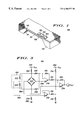
- FIG. 1 illustrates an isometric view of a sensor
- FIG. 2 illustrates a side view of a sensor with pressure applied
- FIG. 3 illustrates a schematic diagram of an error compensation circuit.
- a sensor 100 is shown suitable for manufacture as an integrated circuit (IC) using conventional IC processes.
- IC integrated circuit
- a sensor diaphragm 101 is formed by etching material from a substrate 110 , which provides a mechanical base for diaphragm 101 .
- a transducer 102 , a transducer 103 , and an error compensation circuit 104 are formed on an upper surface of pressure sensor 100 .
- Transducers 102 and 103 each produce a sense signal which is coupled to error compensation circuit 104 .
- the etching process which forms diaphragm 101 is preferably an anisotropic etch so that material is removed along a predictable plane 111 of substrate 110 .
- An anisotropic etch facilitates identifying the location of diaphragm edge 112 from the upper surface of sensor 100 for providing a reference for disposing transducers 102 and 103 and error compensation circuit 104 .
- An epitaxial layer 108 is formed on substrate 110 to provide an etch stop during the anisotropic etching process. Epitaxial layer 108 further provides a high quality base for building transducers 102 and 103 and error compensation circuit 104 on sensor 100 .
- epitaxial layer 108 is formed to a thickness of about 15 microns.
- Diaphragm 101 typically has a thickness between 15 and 18 microns, and a width of 1000 to 2000 microns.
- Transducer 102 and transducer 103 are formed in or on top of epitaxial layer 108 for sensing a deformation of diaphragm 101 when a pressure is applied.
- Transducers 102 and 103 each typically comprise a piezoresistive device such as a Wheatstone bridge or pressure-sensitive resistor.
- Another example of transducer 103 is disclosed in U.S. Pat. No. 4,317,126 and is hereby incorporated by reference.
- Yet another example of transducer 103 is disclosed in U.S. patent application Ser. No. 08/395,228, filed Feb. 27, 1995 by Brian D. Meyer et al. and assigned to Motorola, Inc.
- Transducers 102 and 103 provide transducer output voltages as a function of the displacement of diaphragm 101 .
- FIG. 2 a cross-sectional side view of sensor 100 is shown (not to scale) comprising substrate 110 and diaphragm 101 over which is formed epitaxial layer 108 .
- a pressure applied to sensor 100 causes a deflection of diaphragm 101 .
- Transducer 102 is disposed on diaphragm 101 at location 202 and transducer 103 is disposed on diaphragm 101 at location 203 .
- An error compensation circuit 104 is formed on substrate 110 at a location where pressure-induced stresses in diaphragm 101 do not affect the operation of error compensation circuit 104 .
- error compensation circuit 104 is shown in FIG.
- a location 206 defines a point of symmetry where diaphragm 101 has a maximum deflection. Location 206 is typically located at the midpoint of diaphragm 101 assuming a uniform pressure distribution.
- a plurality of stress mechanisms are induced in diaphragm 101 when diaphragm 101 is deflected in response to the applied pressure.
- One of the stress mechanisms known as bending stress is proportional to the deflection and results from bending of diaphragm 101 upon application of the applied pressure.
- the bending stress is proportional to the magnitude of bending at any point along diaphragm 101 .
- the sensor output signal varies linearly with the bending stress. Therefore, the bending stress is an accurate indicator of the applied pressure.
- the magnitude of bending varies at different points on diaphragm 101 .
- the bending stress appears as a tensile stress on the upper surface of diaphragm 101 in the region between diaphragm edge 112 and location 202 , and as a compressive stress on the upper surface of diaphragm 101 in the region between location 202 and location 203 .
- the bending stress due to tensile stress begins at diaphragm edge 112 and increases to a maximum value at location 203 .
- the tensile stress decreases to zero in the region between location 203 and location 202 .
- diaphragm 101 is subjected to increasing compressive stress which reaches a maximum at location 206 . Therefore, location 202 is the transition point from a region of decreasing tensile stress to a region of increasing compressive stress in diaphragm 101 .
- the bending stress at location 202 is substantially zero.
- Location 203 is a point on the upper surface of diaphragm 101 in the region of tensile stress where bending stress is at a local maximum.
- the point of maximum bending stress i.e. location 203 , does not change significantly as a function of applied pressure. Therefore, transducer 103 is typically disposed at location 203 in order to produce the maximum piezoresistive variation and maximum sense signal from transducer 103 .
- the substantial bending stress at location 203 of diaphragm 101 produces a linear component in the sense signal of transducer 103 which is therefore representative of the applied pressure.
- Membrane stress is another type of stress induced in diaphragm 101 when applied pressure causes diaphragm 101 to stretch. Membrane stress is essentially constant along diaphragm 101 . Thus, the membrane stress present at location 202 is equal to the membrane stress present at location 203 . Membrane stress produces a negative nonlinear error component which reduces the magnitude of the sensor signal from transducer 103 . With the membrane stress acting on diaphragm 101 , the sensor signal from transducer 103 is not truly representative of the applied pressure. Where diaphragm 101 is say sixteen microns thick and has a width of say 1,200 microns, the nonlinear error component becomes significant when the applied pressure deflects diaphragm 101 approximately six microns.
- Transducer 102 is disposed on diaphragm 101 at location 202 , a location having substantially zero bending and substantially zero bending stress.
- the sense signal produced by transducer 102 has a substantially zero linear component.
- the sense signal produced by transducer 102 is a nonlinear error signal produced by membrane stress in diaphragm 101 .
- the bending stress is not present at location 202 and therefore is not present in the sensor signal from transducer 102 .
- the uniform membrane stress in diaphragm 101 produces a membrane stress at location 202 which is equal to the membrane stress at location 203 , so that the nonlinear error signal produced by transducer 102 is equal to the nonlinear error component of the sense signal produced by transducer 103 .
- the sense signals produced by transducers 102 and 103 are respectively coupled to error compensation circuit 104 , which adds the transducer 102 sense signal from the transducer 103 sense signal to produce an output sense signal of sensor 100 whose nonlinear component is substantially
- Locations 202 and 203 are typically determined during the design phase of sensor 100 by modeling sensor 100 using a well-known finite element analysis.
- the finite element analysis is performed in order to predict the behavior of diaphragm 101 when pressure is applied and to analyze the local stresses induced in diaphragm 101 prior to mass producing sensor 100 .
- the modeling of sensor 100 is based on input data describing the structural geometry and materials comprising sensor 100 .
- the input data include such information as the physical dimensions of sensor 100 , the range of applied pressure over which sensor 100 operates, and physical parameters, such as Young's modulus and Poisson's ratio, which characterize the semiconductor material comprising sensor 100 .
- the finite element analysis calculates the magnitude of stress at each point along diaphragm 101 as a function of applied pressure.
- Output data are provided either graphically as a contour plot, or in tabular form. From the tables or contour plots, location 202 and location 203 , the points of maximum and minimum bending stress, are readily apparent. Each of the locations 202 and 203 can be shown to be fixed locations which do not change when applied pressure changes the deflection of diaphragm 101 .
- a sensing structure is defined as the portion of a sensor which produces a stress in response to a physical condition.
- a transducer converts the stress to an electrical sense signal.
- the sensor 100 shown in FIG. 2 is an embodiment of sensor 100 which is a pressure sensor having a sensing structure which is diaphragm 101 . It is understood that similar principles could be used to produce alternative embodiments of sensor 100 , such as an acceleration sensor in which the sensing structure is a beam which is deflected in response to an applied acceleration, or a temperature sensor in which the sensing structure is a bi-metallic element which is deflected in response to a temperature change.
- Transducer 103 is shown as a conventional Wheatstone bridge coupled at node 360 to a resistor 302 and at node 362 to a resistor 304 .
- Resistor 304 is coupled to a power supply conductor 350 operating at ground potential.
- Transducer 103 has an output terminal 356 coupled to a non-inverting input of amplifier 330 and an output terminal 354 coupled to a non-inverting input of amplifier 332 .
- Transducer 103 is comprised of piezoresistive resistors having a positive temperature coefficient. Resistors 302 and 304 have temperature coefficients which are preferably zero such that the potential between nodes 360 and 362 increases with increasing temperature to provide a more constant sense signal across output terminals 354 and 356 . Transducer 103 is disposed at location 203 of diaphragm 101 such that the signal provided at the output of transducer 103 has a linear bending stress component as well as a nonlinear membrane stress component.
- Transducer 102 includes resistors 322 and 324 serially coupled between nodes 360 and 362 . Resistors 322 and 324 are commonly coupled to an output terminal 366 of transducer 102 . Typically, resistor 322 is a piezoresistive element whose resistance varies with applied pressure to produce a sense signal at output terminal 366 of transducer 102 . Resistor 324 can be a piezoresistive element whose resistance varies in response to pressure applied to sensor 100 .
- Transducer 102 is disposed on diaphragm 101 at location 202 , a point on the upper surface of diaphragm 101 having substantially zero bending. Therefore, the sense signal provided at output terminal 366 of transducer 102 is a nonlinear error signal resulting from membrane stress in diaphragm 101 with a substantially zero linear component.
- the sense signal produced at output terminal 366 of transducer 102 is shown as a single-ended sense signal. It is understood that one of ordinary skill in the art could modify transducer 102 in accordance with the principles of the present invention to provide a differential output signal.
- error compensation circuit 104 corrects for the negative nonlinear error in the sensor signal from transducer 103 by adding the sense signal of transducer 102 to the sense signal of transducer 103 .
- An amplifier stage comprising amplifier 330 , resister 306 , resister 308 , and resistor 310 receives the sense signal of transducer 103 at terminal 356 for buffering and amplifying.
- An amplifier stage comprising amplifier 334 , resistor 320 , and resistor 312 buffers and amplifies the sense signal of transducer 103 which is provided at terminal 354 .
- Resistors 306 and 308 produce a bias voltage at an inverting input of amplifier 330 for adjusting the temperature coefficient of the zero pressure offset of sensor 100 .
- resistor 310 is preferably equal to resistor 312
- resistor 320 is preferably equal to the equivalent parallel resistance of resistor 306 and 308 .
- Resistors 314 and 318 set the zero-pressure operating point of amplifier 334 .
- Amplifier 332 has a non-inverting input coupled to the output of transducer 103 .
- Amplifier 332 is configured as a unity gain amplifier which provides a buffer stage to avoid loading transducer 102 .
- Resistors 316 and 312 comprise a summing circuit which sums the respective outputs of amplifiers 332 and 330 at a non-inverting input of amplifier 334 . Recall that output terminal 354 of transducer 103 is coupled to a non-inverting input of amplifier 334 , whereas the output of amplifier 330 is coupled to the inverting input of amplifier 334 .
- Amplifier 334 cancels the negative nonlinear component of the sense signal from transducer 103 by adding the sense signal of transducer 102 to the sense signal of transducer 103 .
- the error corrected output sense signal V OUT is a linear output signal which is representative of the physical condition of sensor 100 .
- Resistor 320 sets the voltage gain of amplifier 334 to produce the desired amplitude of output sense signal V OUT of sensor 100 .
- the Wheatstone bridge arrangement of transducer 102 may be oriented such that the nonlinear error signal due to membrane stress adds to the linear component of the sensor signal due to bending stress. In that case, the nonlinear error signal from transducer 102 is subtracted from the sensor signal from transducer 103 to produce a linear, error corrected output sense signal V OUT which is representative of the physical condition of sensor 100 .
- the present invention provides a circuit and method for correcting an error in a sense signal of a sensor subjected to a bending stress and a membrane stress, where the bending stress linearly represents a physical condition of the sensor and the membrane stress introduces a nonlinear error component into the sense signal.
- a transducer is disposed at a location of maximum bending stress in the sensing structure to produce a sense signal having a maximum linear component as well as the nonlinear error component.
- Another transducer is disposed at a location of minimum bending stress to produce a signal having the nonlinear error component but a substantially zero linear component.
- the sense signals from the two transducers are combined to cancel the nonlinear error component.
- a resulting output signal of the sensor is substantially linear and therefore representative of the sensed physical condition.
Abstract
Description
Claims (21)
Priority Applications (6)
| Application Number | Priority Date | Filing Date | Title |
|---|---|---|---|
| US08/722,384 US6308577B1 (en) | 1996-09-30 | 1996-09-30 | Circuit and method of compensating for membrane stress in a sensor |
| TW086113199A TW345748B (en) | 1996-09-30 | 1997-09-11 | Circuit and method of compensating for membrane stress in a sensor |
| CN97117023A CN1089161C (en) | 1996-09-30 | 1997-09-26 | Compensating circuit of thin film stress in sensor and method |
| JP9279406A JPH10111200A (en) | 1996-09-30 | 1997-09-29 | Circuit and method for compensating film stress at sensor |
| EP97116849A EP0833137A3 (en) | 1996-09-30 | 1997-09-29 | Circuit and method of compensating for membrane stress in a sensor |
| KR1019970051242A KR19980025190A (en) | 1996-09-30 | 1997-09-30 | Film stress compensation circuit and method in sensor |
Applications Claiming Priority (1)
| Application Number | Priority Date | Filing Date | Title |
|---|---|---|---|
| US08/722,384 US6308577B1 (en) | 1996-09-30 | 1996-09-30 | Circuit and method of compensating for membrane stress in a sensor |
Publications (1)
| Publication Number | Publication Date |
|---|---|
| US6308577B1 true US6308577B1 (en) | 2001-10-30 |
Family
ID=24901612
Family Applications (1)
| Application Number | Title | Priority Date | Filing Date |
|---|---|---|---|
| US08/722,384 Expired - Fee Related US6308577B1 (en) | 1996-09-30 | 1996-09-30 | Circuit and method of compensating for membrane stress in a sensor |
Country Status (6)
| Country | Link |
|---|---|
| US (1) | US6308577B1 (en) |
| EP (1) | EP0833137A3 (en) |
| JP (1) | JPH10111200A (en) |
| KR (1) | KR19980025190A (en) |
| CN (1) | CN1089161C (en) |
| TW (1) | TW345748B (en) |
Cited By (4)
| Publication number | Priority date | Publication date | Assignee | Title |
|---|---|---|---|---|
| US20080022779A1 (en) * | 2004-09-24 | 2008-01-31 | Grundfos A/S | Pressure Sensor |
| US20090126498A1 (en) * | 2005-04-18 | 2009-05-21 | Markus Gilch | Pressure sensor device |
| US8132465B1 (en) | 2007-08-01 | 2012-03-13 | Silicon Microstructures, Inc. | Sensor element placement for package stress compensation |
| US20180010975A1 (en) * | 2016-07-08 | 2018-01-11 | Azbil Corporation | Pressure sensor |
Families Citing this family (11)
| Publication number | Priority date | Publication date | Assignee | Title |
|---|---|---|---|---|
| US6056888A (en) * | 1999-04-19 | 2000-05-02 | Motorola, Inc. | Electronic component and method of manufacture |
| DE19957556A1 (en) * | 1999-11-30 | 2001-05-31 | Bosch Gmbh Robert | Semiconductor pressure sensor and measuring device for measuring differential pressure on sensor |
| JP2002310826A (en) * | 2001-02-08 | 2002-10-23 | Tgk Co Ltd | Adjusting method of pressure sensor |
| JP4228827B2 (en) * | 2003-07-31 | 2009-02-25 | パナソニック電工株式会社 | Piezoelectric ultrasonic sensor and method for adjusting resonance frequency thereof |
| US7006938B2 (en) * | 2004-06-16 | 2006-02-28 | Ami Semiconductor, Inc. | Reactive sensor modules using Pade' Approximant based compensation and providing module-sourced excitation |
| US9562820B2 (en) | 2013-02-28 | 2017-02-07 | Mks Instruments, Inc. | Pressure sensor with real time health monitoring and compensation |
| US10027078B2 (en) | 2014-01-02 | 2018-07-17 | Sears Brands, L.L.C. | Slide battery and power tool for use with both slide and post batteries |
| DE102015104410B4 (en) * | 2015-03-24 | 2018-09-13 | Tdk-Micronas Gmbh | pressure sensor |
| US10553843B2 (en) | 2016-03-28 | 2020-02-04 | Transform Sr Brands Llc | Portable power tool, battery pack, and cell configurations for same |
| CN107192556B (en) * | 2017-05-12 | 2019-07-02 | 重庆交通大学 | Miniature constant volume combustion space test device |
| CN114152369A (en) * | 2020-09-07 | 2022-03-08 | 中国科学院微电子研究所 | MEMS piezoresistive pressure sensor and piezoresistive arrangement method |
Citations (8)
| Publication number | Priority date | Publication date | Assignee | Title |
|---|---|---|---|---|
| US3663833A (en) | 1970-04-02 | 1972-05-16 | Monsanto Co | Square root extractor for a process control system |
| US4317126A (en) | 1980-04-14 | 1982-02-23 | Motorola, Inc. | Silicon pressure sensor |
| US4800759A (en) | 1987-08-31 | 1989-01-31 | Yokogawa Electric Corporation | Semiconductor pressure converter |
| US5092177A (en) * | 1989-07-27 | 1992-03-03 | Sextant Avionique | Device for measuring the deformations of a diaphragm |
| US5107710A (en) * | 1990-01-08 | 1992-04-28 | Degussa | Pressure sensor |
| US5166892A (en) * | 1990-04-30 | 1992-11-24 | Yamato Scale Company, Limited | Device for compensating for time-dependent error due to creep and like of measuring apparatus |
| US5193394A (en) * | 1990-02-08 | 1993-03-16 | Nec Corporation | Transducing device for accurately transducing a physical quantity into an electric signal |
| US5291788A (en) * | 1991-09-24 | 1994-03-08 | Kabushiki Kaisha Toshiba | Semiconductor pressure sensor |
Family Cites Families (11)
| Publication number | Priority date | Publication date | Assignee | Title |
|---|---|---|---|---|
| US3743926A (en) * | 1972-04-06 | 1973-07-03 | Gen Electric | Fine linearity control in integral silicon transducers |
| US3772628A (en) * | 1972-05-30 | 1973-11-13 | Gen Electric | Integral silicon diaphragms for low pressure measurements |
| US4050313A (en) * | 1975-06-04 | 1977-09-27 | Hitachi, Ltd. | Semiconductor pressure transducer |
| US4476726A (en) * | 1982-08-19 | 1984-10-16 | Kulite Semiconductor Products, Inc. | Pressure transducers exhibiting linear pressure operation |
| JPS59127876A (en) * | 1983-01-13 | 1984-07-23 | Nec Corp | Diaphragm type semiconductor pressure sensor |
| JPS62204580A (en) * | 1986-03-05 | 1987-09-09 | Fujikura Ltd | Improvement of linearity of semiconductor pressure sensor |
| JPH01109231A (en) * | 1987-10-22 | 1989-04-26 | Komatsu Ltd | Pressure sensor |
| JPH01253622A (en) * | 1988-04-01 | 1989-10-09 | Kyowa Electron Instr Co Ltd | Diaphragm type load transducer |
| JPH02150732A (en) * | 1988-12-01 | 1990-06-11 | Fuji Electric Co Ltd | Compensation circuit for pressure transducer |
| DE59006238D1 (en) * | 1989-12-06 | 1994-07-28 | Siemens Ag Albis | Force converter. |
| US5188983A (en) * | 1990-04-11 | 1993-02-23 | Wisconsin Alumni Research Foundation | Polysilicon resonating beam transducers and method of producing the same |
-
1996
- 1996-09-30 US US08/722,384 patent/US6308577B1/en not_active Expired - Fee Related
-
1997
- 1997-09-11 TW TW086113199A patent/TW345748B/en not_active IP Right Cessation
- 1997-09-26 CN CN97117023A patent/CN1089161C/en not_active Expired - Fee Related
- 1997-09-29 EP EP97116849A patent/EP0833137A3/en not_active Ceased
- 1997-09-29 JP JP9279406A patent/JPH10111200A/en active Pending
- 1997-09-30 KR KR1019970051242A patent/KR19980025190A/en not_active Application Discontinuation
Patent Citations (8)
| Publication number | Priority date | Publication date | Assignee | Title |
|---|---|---|---|---|
| US3663833A (en) | 1970-04-02 | 1972-05-16 | Monsanto Co | Square root extractor for a process control system |
| US4317126A (en) | 1980-04-14 | 1982-02-23 | Motorola, Inc. | Silicon pressure sensor |
| US4800759A (en) | 1987-08-31 | 1989-01-31 | Yokogawa Electric Corporation | Semiconductor pressure converter |
| US5092177A (en) * | 1989-07-27 | 1992-03-03 | Sextant Avionique | Device for measuring the deformations of a diaphragm |
| US5107710A (en) * | 1990-01-08 | 1992-04-28 | Degussa | Pressure sensor |
| US5193394A (en) * | 1990-02-08 | 1993-03-16 | Nec Corporation | Transducing device for accurately transducing a physical quantity into an electric signal |
| US5166892A (en) * | 1990-04-30 | 1992-11-24 | Yamato Scale Company, Limited | Device for compensating for time-dependent error due to creep and like of measuring apparatus |
| US5291788A (en) * | 1991-09-24 | 1994-03-08 | Kabushiki Kaisha Toshiba | Semiconductor pressure sensor |
Cited By (8)
| Publication number | Priority date | Publication date | Assignee | Title |
|---|---|---|---|---|
| US20080022779A1 (en) * | 2004-09-24 | 2008-01-31 | Grundfos A/S | Pressure Sensor |
| US7509866B2 (en) | 2004-09-24 | 2009-03-31 | Grundfos A/S | Pressure sensor |
| US20090211362A1 (en) * | 2004-09-24 | 2009-08-27 | Grundfos A/S | Pressure sensor |
| US7823456B2 (en) | 2004-09-24 | 2010-11-02 | Grundfos A/S | Pressure sensor |
| US20090126498A1 (en) * | 2005-04-18 | 2009-05-21 | Markus Gilch | Pressure sensor device |
| US8132465B1 (en) | 2007-08-01 | 2012-03-13 | Silicon Microstructures, Inc. | Sensor element placement for package stress compensation |
| US20180010975A1 (en) * | 2016-07-08 | 2018-01-11 | Azbil Corporation | Pressure sensor |
| US10451507B2 (en) * | 2016-07-08 | 2019-10-22 | Azbil Corporation | Pressure sensor |
Also Published As
| Publication number | Publication date |
|---|---|
| EP0833137A2 (en) | 1998-04-01 |
| KR19980025190A (en) | 1998-07-06 |
| EP0833137A3 (en) | 1999-05-19 |
| CN1178900A (en) | 1998-04-15 |
| CN1089161C (en) | 2002-08-14 |
| TW345748B (en) | 1998-11-21 |
| JPH10111200A (en) | 1998-04-28 |
Similar Documents
| Publication | Publication Date | Title |
|---|---|---|
| US6308577B1 (en) | Circuit and method of compensating for membrane stress in a sensor | |
| EP0409213B1 (en) | Amplifiying compensation circuit for semiconductor pressure sensor | |
| KR900004369B1 (en) | Bridge circuit | |
| US4480478A (en) | Pressure sensor employing semiconductor strain gauge | |
| JP3399953B2 (en) | Pressure sensor | |
| US4419620A (en) | Linearizing circuits for a semiconductor pressure transducer | |
| EP0034807B1 (en) | Semiconductor strain gauge | |
| WO1988006719A1 (en) | Transducer signal conditioner | |
| US3739644A (en) | Linearization of differential pressure integral silicon transducer | |
| US6877379B2 (en) | Doubly compensated pressure transducer | |
| JPH0972805A (en) | Semiconductor sensor | |
| Zhang et al. | A high-accuracy multi-element silicon barometric pressure sensor | |
| JP2895262B2 (en) | Composite sensor | |
| US4611129A (en) | Signal conversion circuit | |
| US5770965A (en) | Circuit and method of compensating for non-linearities in a sensor signal | |
| JPS59217374A (en) | Semiconductor strain converter | |
| JP2934538B2 (en) | Transducer circuit and manufacturing method thereof | |
| JPH07260824A (en) | Semiconductor sensor of physical quantity | |
| JP2948958B2 (en) | Transducer circuit | |
| US20040031310A1 (en) | Weight measuring apparatus | |
| JPS6057016B2 (en) | Pressure/differential pressure transmitter | |
| JP2608637B2 (en) | Capacitive load cell | |
| Moghimi | Bridge-type sensor measurements are enhanced by autozeroed instrumentation amplifiers with digitally programmable gain and output offset | |
| SU1589088A1 (en) | Semiconductor transducer | |
| KR19980084452A (en) | Temperature compensation circuit of pressure sensor |
Legal Events
| Date | Code | Title | Description |
|---|---|---|---|
| AS | Assignment |
Owner name: MOTOROLA, INC., ILLINOIS Free format text: ASSIGNMENT OF ASSIGNORS INTEREST;ASSIGNORS:BASKETT, IRA E.;MCNEIL, ANDREW C.;REEL/FRAME:008253/0128 Effective date: 19960930 |
|
| CC | Certificate of correction | ||
| AS | Assignment |
Owner name: FREESCALE SEMICONDUCTOR, INC., TEXAS Free format text: ASSIGNMENT OF ASSIGNORS INTEREST;ASSIGNOR:MOTOROLA, INC.;REEL/FRAME:015698/0657 Effective date: 20040404 Owner name: FREESCALE SEMICONDUCTOR, INC.,TEXAS Free format text: ASSIGNMENT OF ASSIGNORS INTEREST;ASSIGNOR:MOTOROLA, INC.;REEL/FRAME:015698/0657 Effective date: 20040404 |
|
| FPAY | Fee payment |
Year of fee payment: 4 |
|
| AS | Assignment |
Owner name: CITIBANK, N.A. AS COLLATERAL AGENT, NEW YORK Free format text: SECURITY AGREEMENT;ASSIGNORS:FREESCALE SEMICONDUCTOR, INC.;FREESCALE ACQUISITION CORPORATION;FREESCALE ACQUISITION HOLDINGS CORP.;AND OTHERS;REEL/FRAME:018855/0129 Effective date: 20061201 Owner name: CITIBANK, N.A. AS COLLATERAL AGENT,NEW YORK Free format text: SECURITY AGREEMENT;ASSIGNORS:FREESCALE SEMICONDUCTOR, INC.;FREESCALE ACQUISITION CORPORATION;FREESCALE ACQUISITION HOLDINGS CORP.;AND OTHERS;REEL/FRAME:018855/0129 Effective date: 20061201 |
|
| REMI | Maintenance fee reminder mailed | ||
| LAPS | Lapse for failure to pay maintenance fees | ||
| STCH | Information on status: patent discontinuation |
Free format text: PATENT EXPIRED DUE TO NONPAYMENT OF MAINTENANCE FEES UNDER 37 CFR 1.362 |
|
| FP | Expired due to failure to pay maintenance fee |
Effective date: 20091030 |
|
| AS | Assignment |
Owner name: FREESCALE SEMICONDUCTOR, INC., TEXAS Free format text: PATENT RELEASE;ASSIGNOR:CITIBANK, N.A., AS COLLATERAL AGENT;REEL/FRAME:037354/0225 Effective date: 20151207 |