US6322201B1 - Printhead with a fluid channel therethrough - Google Patents
Printhead with a fluid channel therethrough Download PDFInfo
- Publication number
- US6322201B1 US6322201B1 US08/956,235 US95623597A US6322201B1 US 6322201 B1 US6322201 B1 US 6322201B1 US 95623597 A US95623597 A US 95623597A US 6322201 B1 US6322201 B1 US 6322201B1
- Authority
- US
- United States
- Prior art keywords
- channel
- printhead
- fluid channel
- firing
- substrate
- Prior art date
- Legal status (The legal status is an assumption and is not a legal conclusion. Google has not performed a legal analysis and makes no representation as to the accuracy of the status listed.)
- Expired - Fee Related
Links
- 239000012530 fluid Substances 0.000 title claims abstract description 26
- 238000010304 firing Methods 0.000 claims abstract description 42
- 239000000758 substrate Substances 0.000 claims abstract description 28
- 238000010438 heat treatment Methods 0.000 claims abstract description 13
- 238000007639 printing Methods 0.000 claims description 35
- 239000010409 thin film Substances 0.000 claims description 24
- 230000008878 coupling Effects 0.000 claims description 2
- 238000010168 coupling process Methods 0.000 claims description 2
- 238000005859 coupling reaction Methods 0.000 claims description 2
- 238000000034 method Methods 0.000 description 30
- 239000000463 material Substances 0.000 description 24
- 230000008569 process Effects 0.000 description 24
- 238000004519 manufacturing process Methods 0.000 description 14
- 238000002161 passivation Methods 0.000 description 12
- XUIMIQQOPSSXEZ-UHFFFAOYSA-N Silicon Chemical compound [Si] XUIMIQQOPSSXEZ-UHFFFAOYSA-N 0.000 description 11
- 229910052710 silicon Inorganic materials 0.000 description 11
- 239000010703 silicon Substances 0.000 description 11
- 238000005530 etching Methods 0.000 description 8
- 239000000945 filler Substances 0.000 description 8
- PXHVJJICTQNCMI-UHFFFAOYSA-N Nickel Chemical compound [Ni] PXHVJJICTQNCMI-UHFFFAOYSA-N 0.000 description 4
- 238000004891 communication Methods 0.000 description 4
- 239000004642 Polyimide Substances 0.000 description 3
- KWYUFKZDYYNOTN-UHFFFAOYSA-M Potassium hydroxide Chemical compound [OH-].[K+] KWYUFKZDYYNOTN-UHFFFAOYSA-M 0.000 description 3
- 238000003491 array Methods 0.000 description 3
- 238000009413 insulation Methods 0.000 description 3
- 229910052751 metal Inorganic materials 0.000 description 3
- 239000002184 metal Substances 0.000 description 3
- 230000002093 peripheral effect Effects 0.000 description 3
- 238000005498 polishing Methods 0.000 description 3
- 229920001721 polyimide Polymers 0.000 description 3
- VYPSYNLAJGMNEJ-UHFFFAOYSA-N Silicium dioxide Chemical compound O=[Si]=O VYPSYNLAJGMNEJ-UHFFFAOYSA-N 0.000 description 2
- 239000000956 alloy Substances 0.000 description 2
- 229910045601 alloy Inorganic materials 0.000 description 2
- RVSGESPTHDDNTH-UHFFFAOYSA-N alumane;tantalum Chemical compound [AlH3].[Ta] RVSGESPTHDDNTH-UHFFFAOYSA-N 0.000 description 2
- 238000010276 construction Methods 0.000 description 2
- 238000000151 deposition Methods 0.000 description 2
- 238000009713 electroplating Methods 0.000 description 2
- 239000010408 film Substances 0.000 description 2
- 239000011521 glass Substances 0.000 description 2
- PCHJSUWPFVWCPO-UHFFFAOYSA-N gold Chemical compound [Au] PCHJSUWPFVWCPO-UHFFFAOYSA-N 0.000 description 2
- 239000012528 membrane Substances 0.000 description 2
- 150000002739 metals Chemical class 0.000 description 2
- 229910052759 nickel Inorganic materials 0.000 description 2
- 238000000059 patterning Methods 0.000 description 2
- 229920002120 photoresistant polymer Polymers 0.000 description 2
- 238000001020 plasma etching Methods 0.000 description 2
- 229910052715 tantalum Inorganic materials 0.000 description 2
- GUVRBAGPIYLISA-UHFFFAOYSA-N tantalum atom Chemical compound [Ta] GUVRBAGPIYLISA-UHFFFAOYSA-N 0.000 description 2
- WGTYBPLFGIVFAS-UHFFFAOYSA-M tetramethylammonium hydroxide Chemical compound [OH-].C[N+](C)(C)C WGTYBPLFGIVFAS-UHFFFAOYSA-M 0.000 description 2
- RYGMFSIKBFXOCR-UHFFFAOYSA-N Copper Chemical compound [Cu] RYGMFSIKBFXOCR-UHFFFAOYSA-N 0.000 description 1
- 229910052581 Si3N4 Inorganic materials 0.000 description 1
- 230000009471 action Effects 0.000 description 1
- 230000002411 adverse Effects 0.000 description 1
- 229910052782 aluminium Inorganic materials 0.000 description 1
- XAGFODPZIPBFFR-UHFFFAOYSA-N aluminium Chemical compound [Al] XAGFODPZIPBFFR-UHFFFAOYSA-N 0.000 description 1
- 230000004888 barrier function Effects 0.000 description 1
- 230000015572 biosynthetic process Effects 0.000 description 1
- 239000004020 conductor Substances 0.000 description 1
- 229910052802 copper Inorganic materials 0.000 description 1
- 239000010949 copper Substances 0.000 description 1
- 230000008021 deposition Effects 0.000 description 1
- 238000005137 deposition process Methods 0.000 description 1
- 238000010586 diagram Methods 0.000 description 1
- 230000000694 effects Effects 0.000 description 1
- 238000005323 electroforming Methods 0.000 description 1
- 238000005516 engineering process Methods 0.000 description 1
- 229920005570 flexible polymer Polymers 0.000 description 1
- 229910052737 gold Inorganic materials 0.000 description 1
- 239000010931 gold Substances 0.000 description 1
- 238000003384 imaging method Methods 0.000 description 1
- 238000007641 inkjet printing Methods 0.000 description 1
- 230000000873 masking effect Effects 0.000 description 1
- 229910001092 metal group alloy Inorganic materials 0.000 description 1
- 238000012986 modification Methods 0.000 description 1
- 230000004048 modification Effects 0.000 description 1
- 238000007517 polishing process Methods 0.000 description 1
- 229910021420 polycrystalline silicon Inorganic materials 0.000 description 1
- 229920000728 polyester Polymers 0.000 description 1
- 229920000642 polymer Polymers 0.000 description 1
- 239000002861 polymer material Substances 0.000 description 1
- 239000004926 polymethyl methacrylate Substances 0.000 description 1
- 229920005591 polysilicon Polymers 0.000 description 1
- 230000004044 response Effects 0.000 description 1
- 239000004065 semiconductor Substances 0.000 description 1
- HBMJWWWQQXIZIP-UHFFFAOYSA-N silicon carbide Chemical compound [Si+]#[C-] HBMJWWWQQXIZIP-UHFFFAOYSA-N 0.000 description 1
- 229910010271 silicon carbide Inorganic materials 0.000 description 1
- 239000000377 silicon dioxide Substances 0.000 description 1
- 235000012239 silicon dioxide Nutrition 0.000 description 1
- HQVNEWCFYHHQES-UHFFFAOYSA-N silicon nitride Chemical compound N12[Si]34N5[Si]62N3[Si]51N64 HQVNEWCFYHHQES-UHFFFAOYSA-N 0.000 description 1
- 239000007787 solid Substances 0.000 description 1
- 238000012876 topography Methods 0.000 description 1
Images


Classifications
-
- B—PERFORMING OPERATIONS; TRANSPORTING
- B41—PRINTING; LINING MACHINES; TYPEWRITERS; STAMPS
- B41J—TYPEWRITERS; SELECTIVE PRINTING MECHANISMS, i.e. MECHANISMS PRINTING OTHERWISE THAN FROM A FORME; CORRECTION OF TYPOGRAPHICAL ERRORS
- B41J2/00—Typewriters or selective printing mechanisms characterised by the printing or marking process for which they are designed
- B41J2/005—Typewriters or selective printing mechanisms characterised by the printing or marking process for which they are designed characterised by bringing liquid or particles selectively into contact with a printing material
- B41J2/01—Ink jet
- B41J2/135—Nozzles
- B41J2/14—Structure thereof only for on-demand ink jet heads
- B41J2/14016—Structure of bubble jet print heads
- B41J2/14145—Structure of the manifold
-
- B—PERFORMING OPERATIONS; TRANSPORTING
- B41—PRINTING; LINING MACHINES; TYPEWRITERS; STAMPS
- B41J—TYPEWRITERS; SELECTIVE PRINTING MECHANISMS, i.e. MECHANISMS PRINTING OTHERWISE THAN FROM A FORME; CORRECTION OF TYPOGRAPHICAL ERRORS
- B41J2/00—Typewriters or selective printing mechanisms characterised by the printing or marking process for which they are designed
- B41J2/005—Typewriters or selective printing mechanisms characterised by the printing or marking process for which they are designed characterised by bringing liquid or particles selectively into contact with a printing material
- B41J2/01—Ink jet
- B41J2/135—Nozzles
- B41J2/14—Structure thereof only for on-demand ink jet heads
- B41J2/14016—Structure of bubble jet print heads
- B41J2/14032—Structure of the pressure chamber
-
- B—PERFORMING OPERATIONS; TRANSPORTING
- B41—PRINTING; LINING MACHINES; TYPEWRITERS; STAMPS
- B41J—TYPEWRITERS; SELECTIVE PRINTING MECHANISMS, i.e. MECHANISMS PRINTING OTHERWISE THAN FROM A FORME; CORRECTION OF TYPOGRAPHICAL ERRORS
- B41J2/00—Typewriters or selective printing mechanisms characterised by the printing or marking process for which they are designed
- B41J2/005—Typewriters or selective printing mechanisms characterised by the printing or marking process for which they are designed characterised by bringing liquid or particles selectively into contact with a printing material
- B41J2/01—Ink jet
- B41J2/135—Nozzles
- B41J2/14—Structure thereof only for on-demand ink jet heads
- B41J2/14016—Structure of bubble jet print heads
- B41J2/14072—Electrical connections, e.g. details on electrodes, connecting the chip to the outside...
-
- B—PERFORMING OPERATIONS; TRANSPORTING
- B41—PRINTING; LINING MACHINES; TYPEWRITERS; STAMPS
- B41J—TYPEWRITERS; SELECTIVE PRINTING MECHANISMS, i.e. MECHANISMS PRINTING OTHERWISE THAN FROM A FORME; CORRECTION OF TYPOGRAPHICAL ERRORS
- B41J2/00—Typewriters or selective printing mechanisms characterised by the printing or marking process for which they are designed
- B41J2/005—Typewriters or selective printing mechanisms characterised by the printing or marking process for which they are designed characterised by bringing liquid or particles selectively into contact with a printing material
- B41J2/01—Ink jet
- B41J2/135—Nozzles
- B41J2/16—Production of nozzles
- B41J2/1601—Production of bubble jet print heads
- B41J2/1603—Production of bubble jet print heads of the front shooter type
-
- B—PERFORMING OPERATIONS; TRANSPORTING
- B41—PRINTING; LINING MACHINES; TYPEWRITERS; STAMPS
- B41J—TYPEWRITERS; SELECTIVE PRINTING MECHANISMS, i.e. MECHANISMS PRINTING OTHERWISE THAN FROM A FORME; CORRECTION OF TYPOGRAPHICAL ERRORS
- B41J2/00—Typewriters or selective printing mechanisms characterised by the printing or marking process for which they are designed
- B41J2/005—Typewriters or selective printing mechanisms characterised by the printing or marking process for which they are designed characterised by bringing liquid or particles selectively into contact with a printing material
- B41J2/01—Ink jet
- B41J2/135—Nozzles
- B41J2/16—Production of nozzles
- B41J2/1621—Manufacturing processes
- B41J2/1625—Manufacturing processes electroforming
-
- B—PERFORMING OPERATIONS; TRANSPORTING
- B41—PRINTING; LINING MACHINES; TYPEWRITERS; STAMPS
- B41J—TYPEWRITERS; SELECTIVE PRINTING MECHANISMS, i.e. MECHANISMS PRINTING OTHERWISE THAN FROM A FORME; CORRECTION OF TYPOGRAPHICAL ERRORS
- B41J2/00—Typewriters or selective printing mechanisms characterised by the printing or marking process for which they are designed
- B41J2/005—Typewriters or selective printing mechanisms characterised by the printing or marking process for which they are designed characterised by bringing liquid or particles selectively into contact with a printing material
- B41J2/01—Ink jet
- B41J2/135—Nozzles
- B41J2/16—Production of nozzles
- B41J2/1621—Manufacturing processes
- B41J2/1626—Manufacturing processes etching
- B41J2/1628—Manufacturing processes etching dry etching
-
- B—PERFORMING OPERATIONS; TRANSPORTING
- B41—PRINTING; LINING MACHINES; TYPEWRITERS; STAMPS
- B41J—TYPEWRITERS; SELECTIVE PRINTING MECHANISMS, i.e. MECHANISMS PRINTING OTHERWISE THAN FROM A FORME; CORRECTION OF TYPOGRAPHICAL ERRORS
- B41J2/00—Typewriters or selective printing mechanisms characterised by the printing or marking process for which they are designed
- B41J2/005—Typewriters or selective printing mechanisms characterised by the printing or marking process for which they are designed characterised by bringing liquid or particles selectively into contact with a printing material
- B41J2/01—Ink jet
- B41J2/135—Nozzles
- B41J2/16—Production of nozzles
- B41J2/1621—Manufacturing processes
- B41J2/1631—Manufacturing processes photolithography
-
- B—PERFORMING OPERATIONS; TRANSPORTING
- B41—PRINTING; LINING MACHINES; TYPEWRITERS; STAMPS
- B41J—TYPEWRITERS; SELECTIVE PRINTING MECHANISMS, i.e. MECHANISMS PRINTING OTHERWISE THAN FROM A FORME; CORRECTION OF TYPOGRAPHICAL ERRORS
- B41J2/00—Typewriters or selective printing mechanisms characterised by the printing or marking process for which they are designed
- B41J2/005—Typewriters or selective printing mechanisms characterised by the printing or marking process for which they are designed characterised by bringing liquid or particles selectively into contact with a printing material
- B41J2/01—Ink jet
- B41J2/135—Nozzles
- B41J2/16—Production of nozzles
- B41J2/1621—Manufacturing processes
- B41J2/1632—Manufacturing processes machining
-
- B—PERFORMING OPERATIONS; TRANSPORTING
- B41—PRINTING; LINING MACHINES; TYPEWRITERS; STAMPS
- B41J—TYPEWRITERS; SELECTIVE PRINTING MECHANISMS, i.e. MECHANISMS PRINTING OTHERWISE THAN FROM A FORME; CORRECTION OF TYPOGRAPHICAL ERRORS
- B41J2/00—Typewriters or selective printing mechanisms characterised by the printing or marking process for which they are designed
- B41J2/005—Typewriters or selective printing mechanisms characterised by the printing or marking process for which they are designed characterised by bringing liquid or particles selectively into contact with a printing material
- B41J2/01—Ink jet
- B41J2/135—Nozzles
- B41J2/16—Production of nozzles
- B41J2/1621—Manufacturing processes
- B41J2/1637—Manufacturing processes molding
- B41J2/1639—Manufacturing processes molding sacrificial molding
-
- B—PERFORMING OPERATIONS; TRANSPORTING
- B41—PRINTING; LINING MACHINES; TYPEWRITERS; STAMPS
- B41J—TYPEWRITERS; SELECTIVE PRINTING MECHANISMS, i.e. MECHANISMS PRINTING OTHERWISE THAN FROM A FORME; CORRECTION OF TYPOGRAPHICAL ERRORS
- B41J2/00—Typewriters or selective printing mechanisms characterised by the printing or marking process for which they are designed
- B41J2/005—Typewriters or selective printing mechanisms characterised by the printing or marking process for which they are designed characterised by bringing liquid or particles selectively into contact with a printing material
- B41J2/01—Ink jet
- B41J2/135—Nozzles
- B41J2/16—Production of nozzles
- B41J2/1621—Manufacturing processes
- B41J2/164—Manufacturing processes thin film formation
- B41J2/1645—Manufacturing processes thin film formation thin film formation by spincoating
Definitions
- This invention relates generally to inkjet printhead fabrication processes and more particularly to methods for fabricating fully integrated inkjet printheads on a substrate.
- An inkjet pen typically includes an ink reservoir and an array of inkjet printing elements.
- the array is formed by an inkjet printhead.
- Each printing element includes a nozzle chamber, a firing resistor and a nozzle opening.
- Ink is stored in the reservoir and passively loaded into respective firing chambers of the printhead via an ink refill channel and respective ink feed channels. Capillary action moves the ink from the reservoir through the refill channel and ink feed channels into the respective firing chambers.
- Printer control circuitry outputs respective signals to the printing elements to activate corresponding firing resistors.
- an activated firing resistor heats ink within the surrounding nozzle chamber causing an expanding vapor bubble to form.
- the bubble forces ink from the nozzle chamber out the nozzle opening.
- An orifice plate adjacent to the barrier layer defines the nozzle openings. The geometry of the nozzle chamber, ink feed channel and nozzle opening defines how quickly a corresponding nozzle chamber is refilled after firing.
- a monolithic structure for an inkjet printhead is described in copending U.S. patent application Ser. No. 08/597,746 filed Feb. 7, 1996 for “Solid State Ink Jet Print Head and Method of Manufacture.”
- the process described therein includes photoimaging techniques similar to those used in semiconductor device manufacturing.
- the printing elements of a monolithic printhead are formed by applying layers to a silicon die.
- the firing resistors, wiring lines and nozzle chambers are formed by applying various passivation, insulation, resistive and conductive layers on the silicon die. Such layers are referred to collectively as a thin film structure.
- An orifice plate overlays the thin film structure opposite the die. Nozzle openings are formed in the orifice plate in alignment with the nozzle chambers and firing resistors. The geometry of the orifice openings affect the size, trajectory and speed of ink drop ejection.
- Orifice plates often are formed of nickel and fabricated by lithographic and electroforming processes.
- a printhead has a substrate with a first surface, an opposite substantially parallel second surface, and an edge surface extending from the first surface to the second surface.
- the substrate further includes a fluid channel that extends from the edge surface inward away from the edge surface and through a recess in the first surface.
- the printhead further has a heating element disposed over the first surface, and a firing chamber disposed over the heating element. The fluid channel directs fluid to the firing chamber through the recess, where the fluid is heated by the heating element and ejected therefrom.
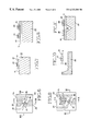
- FIG. 1 is a perspective view of an inkjet pen having a printhead fabricated according to an embodiment of this invention
- FIG. 2 is a block diagram of an embodiment of the inkjet printhead
- FIG. 3 is a partial cross-sectional view of an embodiment of the inkjet printhead fabricated according to one methodology of this invention
- FIG. 4 is a partial plan view of one embodiment of a die having a patterned layer of field oxide
- FIG. 5 is a cross-sectional view taken along line V—V of FIG. 4;
- FIG. 6 is a partial plan view of a printhead in one process embodiment with the thin film structure layers applied and patterned;
- FIG. 7 is a cross-sectional view along line VII—VII of FIG. 6;
- FIG. 8 is a cross-sectional view along line VIII—VIII of FIG. 6;
- FIG. 9 is a partial plan view of a printhead in another process embodiment with the feed channel and fill channels etched out of the die;
- FIG. 10 is a cross-sectional view along line X—X of FIG. 9;
- FIG. 11 is a cross-sectional view along line XI—XI of FIG. 9;
- FIG. 12 is a partial cross-sectional view of a printhead in process with filler material added to the structure of FIG. 9;
- FIG. 13 is a partial cross-sectional view of a printhead in process after polishing and a plasma etching the structure of FIG. 12;
- FIG. 14 is another partial cross-sectional view of a printhead in process after polishing and a plasma etching the structure of FIG. 12;
- FIG. 15 is a partial cross-sectional view of a printhead in process after applying a sacrificial mandrel to the structure of FIGS. 13 and 14;
- FIG. 16 is a partial cross-sectional view of a printhead in process after applying an orifice plate around the sacrificial mandrel of FIG. 15;
- FIG. 17 a partial cross-sectional view of a completed printhead with the sacrificial mandrel of FIG. 15 and filler material removed.
- FIG. 1 shows a scanning-type thermal inkjet pen 10 according to an embodiment of this invention.
- the pen 10 is formed by a pen body 12 , an internal reservoir 14 and a printhead 16 .
- the pen body 12 serves as a housing for the reservoir 14 .
- the reservoir 14 is for storing ink to be ejected from the printhead 16 onto a media sheet.
- the printhead 16 defines an array 22 of printing elements 18 (i.e., nozzle array).
- the nozzle array 22 is formed on a die.
- the reservoir 14 is in physical communication with the nozzle array enabling ink to flow from the reservoir 14 into the printing elements 18 .
- Ink is ejected from a printing element 18 through an opening toward a media sheet to form dots on the media sheet.
- the openings are formed in an orifice layer.
- the orifice layer is a plate attached to the underlying layers.
- the orifice layer is formed integrally with the underlying layers.
- openings also are formed in a flex circuit 20 .
- the flex circuit 20 is a printed circuit made of a flexible base material having multiple conductive paths and a peripheral connector. Conductive paths run from the peripheral connector to the nozzle array 22 .
- the flex circuit 20 is formed from a base material made of polyimide or other flexible polymer material (e.g., polyester, poly-methyl-methacrylate) and conductive paths made of copper, gold or other conductive material.
- the flex circuit 20 with only the base material and conductive paths is available from the 3M Company of Minneapolis, Minn. The nozzle openings and peripheral connector then are added.
- the flex circuit 20 is coupled to off-circuit printer control electronics via an edge connector or button connector. Windows 17 , 19 within the flex circuit 20 facilitate mounting of the printhead 16 to the pen 10 .
- signals are received from the printer control circuitry and activate select printing elements 18 to eject ink at specific times causing a pattern of dots to be output onto a media sheet.
- the pattern of dots forms a desired symbol, character or graphic.
- FIG. 1 Although a scanning-type inkjet pen is shown in FIG. 1, the fabrication processes for the printhead 16 to be described below also apply to printheads for a wide-array printhead, such as a non-scanning page-wide array printhead.
- the printhead 16 includes multiple rows of printing elements 18 .
- two rows 22 , 24 form one set of rows 21
- another two rows 22 , 24 form another set of rows 23 .
- fewer or more rows are included.
- Associated with each printing element 18 is a driver for generating the current level to achieve the desired power levels for heating the element's firing resistor (or heating element).
- logic circuitry for selecting which printing element is active at a given time.
- Driver arrays 43 and logic arrays 44 are depicted in block format.
- the firing resistor (or heating element) of a given printing element is connected to a driver by a wiring line.
- contacts pad arrays 46 for electrically coupling the integrated portion of the printhead to a flex circuit or to off-pen circuitry.
- FIG. 3 shows a printing element 18 of a printhead 16 .
- the printhead includes a silicon die 25 , a thin film structure 27 and an orifice layer 30 .
- the silicon die 25 provides rigidity and in effect serves as a chassis for other portions of the printhead 16 .
- An ink feed channel 29 is formed in the die 25 .
- an ink feed channel 29 is formed for each printing element 18 .
- the thin film structure 27 is formed on the die 25 , and includes various passivation, insulation and conductive layers.
- a firing resistor 26 and conductive traces 28 are formed in the thin film structure 27 for each printing element 18 .
- the orifice layer 30 is formed on the thin film structure 27 opposite the die 25 .
- the orifice layer 30 has an exterior surface 34 which during operation faces a media sheet on which ink is to be printed.
- the orifice layer is either an integral layer formed with the thin film structure 27 or is a plate overlaid on the thin film structure.
- the flex circuit 20 overlays the orifice layer 30 .
- Nozzle chambers 36 and nozzle openings 38 are formed in the orifice layer 30 .
- Each printing element 18 includes a firing resistor 26 , a nozzle chamber 36 , a nozzle opening 38 , and one or more fill channels 40 .
- a center point of the firing resistor 26 defines a normal axis about which components of the printing element 18 are aligned. Specifically it is preferred that the firing resistor 26 be centered within the nozzle chamber 36 and be aligned with the nozzle opening 38 .
- the nozzle chamber 36 in one embodiment is frustoconical in shape.
- One or more fill channels 40 or vias are formed in the thin film structure 27 to couple the nozzle chamber 36 to the feed channel 29 .
- the fill channels 40 are encircled by the nozzle chamber lower periphery 43 so that the ink flowing through a given fill channel 40 flows exclusively into a corresponding nozzle chamber 36 .
- the feed channels 29 for a given set of rows 21 or 23 receive ink from a refill channel that is adjacent an interface between the substrate and the reservoir 14 (not shown).
- the feed channels 29 from one set of printing elements 21 are in communication with one refill channel, while the feed channels 29 from the other set of printing elements 23 are in communication with the other refill channel.
- Such refill channel trough serves both sets of printing elements 21 , 23 .
- the trough receives ink from a pen cartridge reservoir at an edge of the printhead.
- the refill channel 101 does not extend through to the bottom surface 55 of the die 25 .
- the die 25 is a silicon die approximately 675 microns thick. Glass or a stable polymer are used in place of the silicon in alternative embodiments.
- the thin film structure 27 is formed by one or more passivation or insulation layers formed by silicon dioxide, silicon carbide, silicon nitride, tantalum, poly silicon glass, or another suitable material.
- the thin film structure also includes a conductive layer for defining the firing resistor and for defining the conductive traces.
- the conductive layer is formed by tantalum, tantalum-aluminum or another metal or metal alloy.
- the thin film structure is approximately 3 microns thick.
- the orifice layer 30 has a thickness of approximately 10 to 30 microns.
- the nozzle opening 38 has a diameter of approximately 10-30 microns.
- the firing resistor 26 is approximately square with a length on each side of approximately 10-30 microns.
- the base surface 43 of the nozzle chamber 36 supporting the firing resistor 26 has a diameter approximately twice the length of the resistor 26 .
- an anisotropic silicon etch defines 54° wall angles for the feed slot 29 . Although exemplary dimensions and angles are given, such dimensions and angles mary vary for alternative embodiments.
- the die 25 has two sides, a top side 19 and a bottom side 55 .
- the top side defines a top surface and the bottom side defines a bottom surface.
- the die 25 also includes four edges extending between the top side and bottom side.
- the shape and number of edges of the die may vary in alternative embodiments.
- a monolithic inkjet printhead 16 is formed with fabrication processes acting from a single side of the substrate. In some embodiments the fabrication processes also act from an edge during at least one step of the fabrication. According to the invention, however, the fabrication processes need not act from the bottom side of the die 25 .
- substrate refers to the in-process structure of the die 25 and thin film structure 27 , and when present, the orifice layer 30 .
- a layer of field oxide 31 is applied (e.g., grown) to a first side 19 .
- the field oxide layer 25 then is masked and etched as shown in FIGS. 4 and 5 to delimit areas 33 for respective feed channels.
- a membrane region 39 is formed within each feed channel area 33 .
- the feed channel area 33 extends from an edge 35 of the die 25 toward an opposite edge 37 .
- the feed channel 29 will extend from the side edge 35 toward the opposite edge 37 .
- the resulting printhead is to be an edge feed printhead with ink entering the feed channel 29 from the reservoir 14 at the edge 35 (see FIG. 3 ).
- a shelf is formed at the edge and serves as the refill channel 101 .
- the membrane region 39 occurs within the feed channel area 33 and marks regions of the field oxide to remain overlaying the corresponding feed channel 29 . At this stage in the fabrication there is no feed channel etched into the die 25 , just an area 33 delimited by the field oxide layer 31 .
- the field oxide is a first layer of the thin film structure 27 .
- additional layers of the thin film structure 27 are applied to the same side 19 of the die 25 having the field oxide 31 .
- the additional layers are patterned to form firing resistors 26 , wiring lines 28 and passivation 45 as shown in FIGS. 6-8.
- Deposition, masking and etching processes as known in the art are used to apply and pattern the firing resistors 26 , wiring lines 28 and passivation material 45 .
- the firing resistors 26 are formed of tantalum-aluminum and the wiring lines 28 are formed of aluminum.
- different or additional conductive metals, alloys or stacks of metals and/or alloys are used.
- FIG. 6 shows a plan view of a portion of the printhead 16 .
- the entire surface of the substrate is covered with passivation material 45 other than the areas labeled as the die 25 .
- the wiring lines 28 and firing resistor 26 are shown hidden underlying the passivation layer 45 .
- the feed channel 29 still has not been etched in the area 33 .
- the next step is to etch the feed channel 29 and the fill channels 40 .
- An etchant is applied to the top side 19 .
- the die 25 is etched using tetra-methyl ammonium hydroxide, potassium hydroxide or another anisotropic silicon etchant which acts upon the exposed die 25 regions and not upon the passivation 45 .
- the etchant works upon the ⁇ 100> plane of the silicon die to etch the silicon at an angle.
- the etching process continues with the silicon etched away downward at an angle until the angled lines intersect at a given depth.
- the result is a triangular trench for the feed channel 29 as shown in FIGS. 9-11.
- a trench has been created in the die 25 using a process acting from the top side 19 of the die 25 .
- the trench defines the feed channel 29 .
- the feed channels 29 , the fill channels 40 , the firing resistors 26 and the wiring lines 28 have been formed, but the nozzle chambers 36 (see FIG. 3) have not yet been formed.
- the nozzle chambers 36 are to be formed with an orifice plate, with an orifice film or by direct imaging.
- the presence of the feed channel 29 and fill channels 40 can adversely impact the formation of the nozzle chambers 36 due to the varied topography introduced by such voids.
- Such voids are filed up to enable continued processing from the top surface.
- a material 50 of photoresist or polyimide is spun and baked onto the substrate as shown in FIG. 12 .
- the material 50 fills in the feed channel 29 and fill channels 40 and covers the passivation layer 45 .
- a chemical-mechanical polishing process is applied to the substrate to remove the material 50 in areas other than the feed channels 29 and fill channels 40 , as shown in FIGS. 13 and 14.
- an O 2 plasma etch also is performed so that the filler material 50 is removed without removing the passivation material 45 .
- the result is a planar surface with bumps of passivation material 45 over the firing resistors 26 (see FIGS. 13 and 14 ).
- the top side 19 of the substrate now has areas of passivation material 45 and filler material 50 .
- the substrate is ready for processes to form the nozzle chambers 36 .
- a frustoconical sacrificial mandrel 52 is formed over each resistor 26 in the shape of the desired nozzle chamber.
- Such sacrificial mandrel 52 is formed by depositing a suitable material, such as photoresist or polyimide, then patterning and etching the material to the desired shape.
- an orifice layer 30 is applied as shown in FIG. 16 to a thickness flush with the sacrificial mandrel 52 .
- the orifice layer is applied by an electroplating process, in which the substrate is dipped into an electroplating tank. Material (e.g., nickel, gold) forms on the substrate around the sacrificial mandrel 52 .
- nozzle chambers 36 are described as being formed by applying a sacrificial mandrel and orifice layer then etching out the sacrificial mandrel, other processes also may be used.
- an orifice film is applied to the substrate as the substrate appears in FIG. 14 . Patterning and etching processes then are performed to define the nozzle chamber 36 .
- An etching process as described above then is performed to remove the filler material 50 from the feed channel(s) 29 and fill channels 40 .
- material is spun onto the substrate, masked and exposed to form the nozzle chambers 36 . Again an etching process as described above is performed afterward to remove the filler material 50 from the feed channels 29 and fill channels 40 .
Abstract
Description
Claims (6)
Priority Applications (7)
| Application Number | Priority Date | Filing Date | Title |
|---|---|---|---|
| US08/956,235 US6322201B1 (en) | 1997-10-22 | 1997-10-22 | Printhead with a fluid channel therethrough |
| DE19836357A DE19836357B8 (en) | 1997-10-22 | 1998-08-11 | One-sided manufacturing method for forming a monolithic ink jet printing element array on a substrate |
| GB9820523A GB2330557B (en) | 1997-10-22 | 1998-09-21 | Single-side fabrication process for forming inkjet monolithic printing element array on a substrate |
| KR1019980044096A KR100595081B1 (en) | 1997-10-22 | 1998-10-21 | Single-side fabrication process for forming inkjet monolithic printing element array on a substrate |
| JP30001898A JP3340967B2 (en) | 1997-10-22 | 1998-10-21 | Manufacturing method of monolithic ink jet print head |
| US09/378,230 US6365058B1 (en) | 1997-10-22 | 1999-08-19 | Method of manufacturing a fluid ejection device with a fluid channel therethrough |
| US09/378,231 US6137443A (en) | 1997-10-22 | 1999-08-19 | Single-side fabrication process for forming inkjet monolithic printing element array on a substrate |
Applications Claiming Priority (1)
| Application Number | Priority Date | Filing Date | Title |
|---|---|---|---|
| US08/956,235 US6322201B1 (en) | 1997-10-22 | 1997-10-22 | Printhead with a fluid channel therethrough |
Related Child Applications (2)
| Application Number | Title | Priority Date | Filing Date |
|---|---|---|---|
| US09/378,230 Division US6365058B1 (en) | 1997-10-22 | 1999-08-19 | Method of manufacturing a fluid ejection device with a fluid channel therethrough |
| US09/378,231 Continuation US6137443A (en) | 1997-10-22 | 1999-08-19 | Single-side fabrication process for forming inkjet monolithic printing element array on a substrate |
Publications (1)
| Publication Number | Publication Date |
|---|---|
| US6322201B1 true US6322201B1 (en) | 2001-11-27 |
Family
ID=25497967
Family Applications (3)
| Application Number | Title | Priority Date | Filing Date |
|---|---|---|---|
| US08/956,235 Expired - Fee Related US6322201B1 (en) | 1997-10-22 | 1997-10-22 | Printhead with a fluid channel therethrough |
| US09/378,231 Expired - Lifetime US6137443A (en) | 1997-10-22 | 1999-08-19 | Single-side fabrication process for forming inkjet monolithic printing element array on a substrate |
| US09/378,230 Expired - Fee Related US6365058B1 (en) | 1997-10-22 | 1999-08-19 | Method of manufacturing a fluid ejection device with a fluid channel therethrough |
Family Applications After (2)
| Application Number | Title | Priority Date | Filing Date |
|---|---|---|---|
| US09/378,231 Expired - Lifetime US6137443A (en) | 1997-10-22 | 1999-08-19 | Single-side fabrication process for forming inkjet monolithic printing element array on a substrate |
| US09/378,230 Expired - Fee Related US6365058B1 (en) | 1997-10-22 | 1999-08-19 | Method of manufacturing a fluid ejection device with a fluid channel therethrough |
Country Status (5)
| Country | Link |
|---|---|
| US (3) | US6322201B1 (en) |
| JP (1) | JP3340967B2 (en) |
| KR (1) | KR100595081B1 (en) |
| DE (1) | DE19836357B8 (en) |
| GB (1) | GB2330557B (en) |
Cited By (9)
| Publication number | Priority date | Publication date | Assignee | Title |
|---|---|---|---|---|
| US6475402B2 (en) * | 2001-03-02 | 2002-11-05 | Hewlett-Packard Company | Ink feed channels and heater supports for thermal ink-jet printhead |
| US6655787B1 (en) * | 2002-08-26 | 2003-12-02 | Eastman Kodak Company | Drop-on-demand liquid emission using symmetrical electrostatic device |
| EP1403055A1 (en) * | 2002-09-25 | 2004-03-31 | Eastman Kodak Company | Method of fabrication of electrostatic liquid emission device |
| US20050243142A1 (en) * | 2004-04-29 | 2005-11-03 | Shaarawi Mohammed S | Microfluidic architecture |
| US20050243141A1 (en) * | 2004-04-29 | 2005-11-03 | Hewlett-Packard Development Company, L.P. | Fluid ejection device and manufacturing method |
| US20060087882A1 (en) * | 2004-10-26 | 2006-04-27 | Tom Kinsley | Data retention kill function |
| GB2396334B (en) * | 2002-10-31 | 2006-08-09 | Hewlett Packard Development Co | Slotted substrates and methods and systems for forming same |
| KR100717028B1 (en) * | 2005-09-13 | 2007-05-10 | 삼성전자주식회사 | Inkjet printhead having conductive epoxy resin |
| US9308728B2 (en) | 2013-05-31 | 2016-04-12 | Stmicroelectronics, Inc. | Method of making inkjet print heads having inkjet chambers and orifices formed in a wafer and related devices |
Families Citing this family (42)
| Publication number | Priority date | Publication date | Assignee | Title |
|---|---|---|---|---|
| US6305790B1 (en) | 1996-02-07 | 2001-10-23 | Hewlett-Packard Company | Fully integrated thermal inkjet printhead having multiple ink feed holes per nozzle |
| US6543884B1 (en) | 1996-02-07 | 2003-04-08 | Hewlett-Packard Company | Fully integrated thermal inkjet printhead having etched back PSG layer |
| US6336714B1 (en) * | 1996-02-07 | 2002-01-08 | Hewlett-Packard Company | Fully integrated thermal inkjet printhead having thin film layer shelf |
| IT1309735B1 (en) * | 1999-12-27 | 2002-01-30 | Olivetti Lexikon Spa | INK MULTIPLE CHANNEL HEAD |
| US6482574B1 (en) * | 2000-04-20 | 2002-11-19 | Hewlett-Packard Co. | Droplet plate architecture in ink-jet printheads |
| IT1320392B1 (en) | 2000-06-05 | 2003-11-26 | Olivetti Lexikon Spa | MANUFACTURING PROCESS OF A MONOLITHIC PRINT HEAD CONUGELLI TRUNCATED-CONICAL. |
| US6402301B1 (en) | 2000-10-27 | 2002-06-11 | Lexmark International, Inc | Ink jet printheads and methods therefor |
| US6364466B1 (en) * | 2000-11-30 | 2002-04-02 | Hewlett-Packard Company | Particle tolerant ink-feed channel structure for fully integrated inkjet printhead |
| KR100506079B1 (en) * | 2000-12-05 | 2005-08-04 | 삼성전자주식회사 | Bubble-jet type inkjet print head |
| US6675476B2 (en) | 2000-12-05 | 2004-01-13 | Hewlett-Packard Development Company, L.P. | Slotted substrates and techniques for forming same |
| US6450619B1 (en) * | 2001-02-22 | 2002-09-17 | Eastman Kodak Company | CMOS/MEMS integrated ink jet print head with heater elements formed during CMOS processing and method of forming same |
| US6471340B2 (en) | 2001-02-12 | 2002-10-29 | Hewlett-Packard Company | Inkjet printhead assembly |
| US7160806B2 (en) * | 2001-08-16 | 2007-01-09 | Hewlett-Packard Development Company, L.P. | Thermal inkjet printhead processing with silicon etching |
| US6698868B2 (en) * | 2001-10-31 | 2004-03-02 | Hewlett-Packard Development Company, L.P. | Thermal drop generator for ultra-small droplets |
| US7125731B2 (en) * | 2001-10-31 | 2006-10-24 | Hewlett-Packard Development Company, L.P. | Drop generator for ultra-small droplets |
| US6627467B2 (en) | 2001-10-31 | 2003-09-30 | Hewlett-Packard Development Company, Lp. | Fluid ejection device fabrication |
| US6962402B2 (en) * | 2002-12-02 | 2005-11-08 | Silverbrook Research Pty Ltd | Inkjet printhead with ink supply passage formed from both sides of the wafer by overlapping etches |
| JP3856123B2 (en) * | 2002-04-17 | 2006-12-13 | セイコーエプソン株式会社 | MASK AND ITS MANUFACTURING METHOD, ELECTROLUMINESCENT DEVICE, ITS MANUFACTURING METHOD, AND ELECTRONIC DEVICE |
| US6767474B2 (en) * | 2002-07-19 | 2004-07-27 | Hewlett-Packard Development Company, L.P. | Fluid ejector head having a planar passivation layer |
| US7581822B2 (en) * | 2002-11-23 | 2009-09-01 | Silverbrook Research Pty Ltd | Inkjet printhead with low voltage ink vaporizing heaters |
| US6672710B1 (en) | 2002-11-23 | 2004-01-06 | Silverbrook Research Pty Ltd | Thermal ink jet printhead with symmetric bubble formation |
| US6692108B1 (en) | 2002-11-23 | 2004-02-17 | Silverbrook Research Pty Ltd. | High efficiency thermal ink jet printhead |
| US7152958B2 (en) | 2002-11-23 | 2006-12-26 | Silverbrook Research Pty Ltd | Thermal ink jet with chemical vapor deposited nozzle plate |
| US6719406B1 (en) * | 2002-11-23 | 2004-04-13 | Silverbrook Research Pty Ltd | Ink jet printhead with conformally coated heater |
| US6755509B2 (en) * | 2002-11-23 | 2004-06-29 | Silverbrook Research Pty Ltd | Thermal ink jet printhead with suspended beam heater |
| KR100468160B1 (en) * | 2002-12-02 | 2005-01-26 | 삼성전자주식회사 | monolithic bubble-ink jet print head and fabrication method therefor |
| US6926390B2 (en) * | 2003-02-05 | 2005-08-09 | Hewlett-Packard Development Company, L.P. | Method of forming mixed-phase compressive tantalum thin films using nitrogen residual gas, thin films and fluid ejection devices including same |
| US6916090B2 (en) | 2003-03-10 | 2005-07-12 | Hewlett-Packard Development Company, L.P. | Integrated fluid ejection device and filter |
| ITTO20030841A1 (en) * | 2003-10-27 | 2005-04-28 | Olivetti I Jet Spa | INKJET PRINT HEAD AND ITS MANUFACTURING PROCESS. |
| KR100517515B1 (en) | 2004-01-20 | 2005-09-28 | 삼성전자주식회사 | Method for manufacturing monolithic inkjet printhead |
| US7322104B2 (en) * | 2004-06-25 | 2008-01-29 | Canon Kabushiki Kaisha | Method for producing an ink jet head |
| US8043517B2 (en) * | 2005-09-19 | 2011-10-25 | Hewlett-Packard Development Company, L.P. | Method of forming openings in substrates and inkjet printheads fabricated thereby |
| JP2007237718A (en) * | 2006-03-13 | 2007-09-20 | Seiko Epson Corp | Manufacturing method for inkjet head |
| WO2009108195A1 (en) * | 2008-02-27 | 2009-09-03 | Hewlett-Packard Development Company, L.P. | Printhead assembly having grooves externally exposing printhead die |
| CN102202896A (en) * | 2008-10-30 | 2011-09-28 | 惠普开发有限公司 | Thermal inkjet printhead feed transition chamber and method of cooling using same |
| JP2013500880A (en) | 2009-07-31 | 2013-01-10 | ヒューレット−パッカード デベロップメント カンパニー エル.ピー. | Inkjet printhead and method using a central ink supply path |
| US8425787B2 (en) * | 2009-08-26 | 2013-04-23 | Hewlett-Packard Development Company, L.P. | Inkjet printhead bridge beam fabrication method |
| US8267504B2 (en) * | 2010-04-27 | 2012-09-18 | Eastman Kodak Company | Printhead including integrated stimulator/filter device |
| US8287101B2 (en) * | 2010-04-27 | 2012-10-16 | Eastman Kodak Company | Printhead stimulator/filter device printing method |
| JP5615450B2 (en) * | 2011-01-31 | 2014-10-29 | ヒューレット−パッカード デベロップメント カンパニー エル.ピー.Hewlett‐Packard Development Company, L.P. | Fluid ejection assembly and associated method |
| US20120210580A1 (en) * | 2011-02-23 | 2012-08-23 | Dietl Steven J | Method of assembling an inkjet printhead |
| JP2015054410A (en) * | 2013-09-10 | 2015-03-23 | キヤノン株式会社 | Liquid discharge head and device |
Citations (17)
| Publication number | Priority date | Publication date | Assignee | Title |
|---|---|---|---|---|
| US3852563A (en) | 1974-02-01 | 1974-12-03 | Hewlett Packard Co | Thermal printing head |
| US4438191A (en) | 1982-11-23 | 1984-03-20 | Hewlett-Packard Company | Monolithic ink jet print head |
| JPS619855A (en) | 1984-06-22 | 1986-01-17 | Tanashin Denki Co | Mode switching device of tape recorder |
| JPS6294347A (en) | 1985-10-22 | 1987-04-30 | Ricoh Seiki Kk | Thermal ink jet printing head |
| EP0244214A1 (en) | 1986-04-28 | 1987-11-04 | Hewlett-Packard Company | Thermal ink jet printhead |
| US4847630A (en) | 1987-12-17 | 1989-07-11 | Hewlett-Packard Company | Integrated thermal ink jet printhead and method of manufacture |
| US4851371A (en) | 1988-12-05 | 1989-07-25 | Xerox Corporation | Fabricating process for large array semiconductive devices |
| US4875968A (en) | 1989-02-02 | 1989-10-24 | Xerox Corporation | Method of fabricating ink jet printheads |
| US4894664A (en) | 1986-04-28 | 1990-01-16 | Hewlett-Packard Company | Monolithic thermal ink jet printhead with integral nozzle and ink feed |
| US5041190A (en) | 1990-05-16 | 1991-08-20 | Xerox Corporation | Method of fabricating channel plates and ink jet printheads containing channel plates |
| US5160577A (en) | 1991-07-30 | 1992-11-03 | Deshpande Narayan V | Method of fabricating an aperture plate for a roof-shooter type printhead |
| US5194877A (en) | 1991-05-24 | 1993-03-16 | Hewlett-Packard Company | Process for manufacturing thermal ink jet printheads having metal substrates and printheads manufactured thereby |
| US5308442A (en) | 1993-01-25 | 1994-05-03 | Hewlett-Packard Company | Anisotropically etched ink fill slots in silicon |
| US5317346A (en) | 1992-03-04 | 1994-05-31 | Hewlett-Packard Company | Compound ink feed slot |
| DE19536429A1 (en) | 1995-09-29 | 1997-04-10 | Siemens Ag | Ink jet printhead and method of making such an ink jet printhead |
| EP0783970A2 (en) | 1996-01-12 | 1997-07-16 | Canon Kabushiki Kaisha | Process for the production of a liquid jet recording head |
| US5851412A (en) * | 1996-03-04 | 1998-12-22 | Xerox Corporation | Thermal ink-jet printhead with a suspended heating element in each ejector |
Family Cites Families (8)
| Publication number | Priority date | Publication date | Assignee | Title |
|---|---|---|---|---|
| US4809428A (en) * | 1987-12-10 | 1989-03-07 | Hewlett-Packard Company | Thin film device for an ink jet printhead and process for the manufacturing same |
| US5211806A (en) * | 1991-12-24 | 1993-05-18 | Xerox Corporation | Monolithic inkjet printhead |
| US5306370A (en) * | 1992-11-02 | 1994-04-26 | Xerox Corporation | Method of reducing chipping and contamination of reservoirs and channels in thermal ink printheads during dicing by vacuum impregnation with protective filler material |
| JP2727988B2 (en) * | 1994-12-15 | 1998-03-18 | 日本電気株式会社 | Method of manufacturing ink jet print head |
| JPH0948123A (en) * | 1995-08-07 | 1997-02-18 | Canon Inc | Ink jet recording head, production thereof, ink jet recording apparatus and data processing apparatus |
| US5883650A (en) * | 1995-12-06 | 1999-03-16 | Hewlett-Packard Company | Thin-film printhead device for an ink-jet printer |
| US6000787A (en) * | 1996-02-07 | 1999-12-14 | Hewlett-Packard Company | Solid state ink jet print head |
| JPH1098557A (en) * | 1996-09-24 | 1998-04-14 | Ricoh Co Ltd | Isdn terminal adapter device |
-
1997
- 1997-10-22 US US08/956,235 patent/US6322201B1/en not_active Expired - Fee Related
-
1998
- 1998-08-11 DE DE19836357A patent/DE19836357B8/en not_active Expired - Fee Related
- 1998-09-21 GB GB9820523A patent/GB2330557B/en not_active Expired - Fee Related
- 1998-10-21 KR KR1019980044096A patent/KR100595081B1/en not_active IP Right Cessation
- 1998-10-21 JP JP30001898A patent/JP3340967B2/en not_active Expired - Fee Related
-
1999
- 1999-08-19 US US09/378,231 patent/US6137443A/en not_active Expired - Lifetime
- 1999-08-19 US US09/378,230 patent/US6365058B1/en not_active Expired - Fee Related
Patent Citations (18)
| Publication number | Priority date | Publication date | Assignee | Title |
|---|---|---|---|---|
| US3852563A (en) | 1974-02-01 | 1974-12-03 | Hewlett Packard Co | Thermal printing head |
| US4438191A (en) | 1982-11-23 | 1984-03-20 | Hewlett-Packard Company | Monolithic ink jet print head |
| JPS5995156A (en) | 1982-11-23 | 1984-06-01 | Yokogawa Hewlett Packard Ltd | Formation of ink chamber |
| JPS619855A (en) | 1984-06-22 | 1986-01-17 | Tanashin Denki Co | Mode switching device of tape recorder |
| JPS6294347A (en) | 1985-10-22 | 1987-04-30 | Ricoh Seiki Kk | Thermal ink jet printing head |
| US4894664A (en) | 1986-04-28 | 1990-01-16 | Hewlett-Packard Company | Monolithic thermal ink jet printhead with integral nozzle and ink feed |
| EP0244214A1 (en) | 1986-04-28 | 1987-11-04 | Hewlett-Packard Company | Thermal ink jet printhead |
| US4847630A (en) | 1987-12-17 | 1989-07-11 | Hewlett-Packard Company | Integrated thermal ink jet printhead and method of manufacture |
| US4851371A (en) | 1988-12-05 | 1989-07-25 | Xerox Corporation | Fabricating process for large array semiconductive devices |
| US4875968A (en) | 1989-02-02 | 1989-10-24 | Xerox Corporation | Method of fabricating ink jet printheads |
| US5041190A (en) | 1990-05-16 | 1991-08-20 | Xerox Corporation | Method of fabricating channel plates and ink jet printheads containing channel plates |
| US5194877A (en) | 1991-05-24 | 1993-03-16 | Hewlett-Packard Company | Process for manufacturing thermal ink jet printheads having metal substrates and printheads manufactured thereby |
| US5160577A (en) | 1991-07-30 | 1992-11-03 | Deshpande Narayan V | Method of fabricating an aperture plate for a roof-shooter type printhead |
| US5317346A (en) | 1992-03-04 | 1994-05-31 | Hewlett-Packard Company | Compound ink feed slot |
| US5308442A (en) | 1993-01-25 | 1994-05-03 | Hewlett-Packard Company | Anisotropically etched ink fill slots in silicon |
| DE19536429A1 (en) | 1995-09-29 | 1997-04-10 | Siemens Ag | Ink jet printhead and method of making such an ink jet printhead |
| EP0783970A2 (en) | 1996-01-12 | 1997-07-16 | Canon Kabushiki Kaisha | Process for the production of a liquid jet recording head |
| US5851412A (en) * | 1996-03-04 | 1998-12-22 | Xerox Corporation | Thermal ink-jet printhead with a suspended heating element in each ejector |
Cited By (18)
| Publication number | Priority date | Publication date | Assignee | Title |
|---|---|---|---|---|
| US6475402B2 (en) * | 2001-03-02 | 2002-11-05 | Hewlett-Packard Company | Ink feed channels and heater supports for thermal ink-jet printhead |
| US6655787B1 (en) * | 2002-08-26 | 2003-12-02 | Eastman Kodak Company | Drop-on-demand liquid emission using symmetrical electrostatic device |
| US6966110B2 (en) | 2002-09-25 | 2005-11-22 | Eastman Kodak Company | Fabrication of liquid emission device with symmetrical electrostatic mandrel |
| EP1403055A1 (en) * | 2002-09-25 | 2004-03-31 | Eastman Kodak Company | Method of fabrication of electrostatic liquid emission device |
| GB2396334B (en) * | 2002-10-31 | 2006-08-09 | Hewlett Packard Development Co | Slotted substrates and methods and systems for forming same |
| US20080198202A1 (en) * | 2004-04-29 | 2008-08-21 | Mohammed Shaarawi | Microfluidic Architecture |
| US20050243141A1 (en) * | 2004-04-29 | 2005-11-03 | Hewlett-Packard Development Company, L.P. | Fluid ejection device and manufacturing method |
| US7293359B2 (en) | 2004-04-29 | 2007-11-13 | Hewlett-Packard Development Company, L.P. | Method for manufacturing a fluid ejection device |
| US20080024559A1 (en) * | 2004-04-29 | 2008-01-31 | Shaarawi Mohammed S | Fluid ejection device |
| US7387370B2 (en) | 2004-04-29 | 2008-06-17 | Hewlett-Packard Development Company, L.P. | Microfluidic architecture |
| US20050243142A1 (en) * | 2004-04-29 | 2005-11-03 | Shaarawi Mohammed S | Microfluidic architecture |
| US7543915B2 (en) | 2004-04-29 | 2009-06-09 | Hewlett-Packard Development Company, L.P. | Fluid ejection device |
| US7798612B2 (en) | 2004-04-29 | 2010-09-21 | Hewlett-Packard Development Company, L.P. | Microfluidic architecture |
| US20060087882A1 (en) * | 2004-10-26 | 2006-04-27 | Tom Kinsley | Data retention kill function |
| KR100717028B1 (en) * | 2005-09-13 | 2007-05-10 | 삼성전자주식회사 | Inkjet printhead having conductive epoxy resin |
| US9308728B2 (en) | 2013-05-31 | 2016-04-12 | Stmicroelectronics, Inc. | Method of making inkjet print heads having inkjet chambers and orifices formed in a wafer and related devices |
| US10124588B2 (en) | 2013-05-31 | 2018-11-13 | Stmicroelectronics, Inc. | Method of making inkjet print heads having inkjet chambers and orifices formed in a wafer and related devices |
| US10843465B2 (en) | 2013-05-31 | 2020-11-24 | Stmicroelectronics, Inc. | Method of making inkjet print heads having inkjet chambers and orifices formed in a wafer and related devices |
Also Published As
| Publication number | Publication date |
|---|---|
| KR19990037265A (en) | 1999-05-25 |
| JPH11192714A (en) | 1999-07-21 |
| GB2330557B (en) | 2001-08-01 |
| DE19836357B8 (en) | 2010-06-10 |
| KR100595081B1 (en) | 2006-09-22 |
| JP3340967B2 (en) | 2002-11-05 |
| GB2330557A (en) | 1999-04-28 |
| GB9820523D0 (en) | 1998-11-11 |
| DE19836357A1 (en) | 1999-04-29 |
| DE19836357B4 (en) | 2010-01-07 |
| US6137443A (en) | 2000-10-24 |
| US6365058B1 (en) | 2002-04-02 |
Similar Documents
| Publication | Publication Date | Title |
|---|---|---|
| US6322201B1 (en) | Printhead with a fluid channel therethrough | |
| JP2994344B2 (en) | Ink jet print head and method of forming the same | |
| JP4355777B2 (en) | Fabrication method of scalable wide array inkjet printhead | |
| EP1132214B1 (en) | Methods of fabricating fit firing chambers of different drop weights on a single printhead | |
| US6767474B2 (en) | Fluid ejector head having a planar passivation layer | |
| JP2001071504A (en) | Printer having ink jet print head, manufacture thereof and method for printing | |
| JPS6280054A (en) | Ink jet type printing head with built-in filter and manufacture thereof | |
| JP2004148824A (en) | Substrate with slot, and forming method | |
| US6457814B1 (en) | Fluid-jet printhead and method of fabricating a fluid-jet printhead | |
| US7837303B2 (en) | Inkjet printhead | |
| JP2001071503A (en) | Printer having ink jet print head, manufacture thereof and method for printing | |
| US6776915B2 (en) | Method of manufacturing a fluid ejection device with a fluid channel therethrough | |
| CN100369749C (en) | Method of fabricating ink jet head | |
| US6039438A (en) | Limiting propagation of thin film failures in an inkjet printhead | |
| JP2002283580A (en) | Ink supply trench etching technique for completely integrated thermal ink-jet printing head | |
| US6935023B2 (en) | Method of forming electrical connection for fluid ejection device | |
| KR100552664B1 (en) | Monolithic ink jet printhead having ink chamber defined by side wall and method of manufacturing thereof | |
| US6457815B1 (en) | Fluid-jet printhead and method of fabricating a fluid-jet printhead | |
| US7478476B2 (en) | Methods of fabricating fit firing chambers of different drop wights on a single printhead | |
| CN108136776B (en) | Fluid ejection apparatus | |
| KR100421027B1 (en) | Inkjet printhead and manufacturing method thereof | |
| KR20060023490A (en) | Ink jet head including cantilever-shaped heater | |
| JP2004001174A (en) | Substrate for fluid discharge device and method for forming substrate |
Legal Events
| Date | Code | Title | Description |
|---|---|---|---|
| AS | Assignment |
Owner name: HEWLETT-PACKARD COMPANY, CALIFORNIA Free format text: ASSIGNMENT OF ASSIGNORS INTEREST;ASSIGNORS:BEATTY, CHRISTOPHER;KAWAMURA, NAOTO;REEL/FRAME:008850/0779;SIGNING DATES FROM 19971020 TO 19971022 |
|
| AS | Assignment |
Owner name: HEWLETT-PACKARD COMPANY, COLORADO Free format text: MERGER;ASSIGNOR:HEWLETT-PACKARD COMPANY;REEL/FRAME:011523/0469 Effective date: 19980520 |
|
| FPAY | Fee payment |
Year of fee payment: 4 |
|
| FPAY | Fee payment |
Year of fee payment: 8 |
|
| AS | Assignment |
Owner name: HEWLETT-PACKARD DEVELOPMENT COMPANY, L.P., TEXAS Free format text: ASSIGNMENT OF ASSIGNORS INTEREST;ASSIGNOR:HEWLETT-PACKARD COMPANY;REEL/FRAME:026945/0699 Effective date: 20030131 |
|
| REMI | Maintenance fee reminder mailed | ||
| LAPS | Lapse for failure to pay maintenance fees | ||
| STCH | Information on status: patent discontinuation |
Free format text: PATENT EXPIRED DUE TO NONPAYMENT OF MAINTENANCE FEES UNDER 37 CFR 1.362 |
|
| FP | Lapsed due to failure to pay maintenance fee |
Effective date: 20131127 |