US6332677B1 - Stable substrate structure for a wide swath nozzle array in a high resolution inkjet printer - Google Patents
Stable substrate structure for a wide swath nozzle array in a high resolution inkjet printer Download PDFInfo
- Publication number
- US6332677B1 US6332677B1 US09/395,379 US39537999A US6332677B1 US 6332677 B1 US6332677 B1 US 6332677B1 US 39537999 A US39537999 A US 39537999A US 6332677 B1 US6332677 B1 US 6332677B1
- Authority
- US
- United States
- Prior art keywords
- substrate
- firing chambers
- printhead
- ink
- end portions
- Prior art date
- Legal status (The legal status is an assumption and is not a legal conclusion. Google has not performed a legal analysis and makes no representation as to the accuracy of the status listed.)
- Expired - Fee Related
Links
- 239000000758 substrate Substances 0.000 title claims abstract description 167
- 238000010304 firing Methods 0.000 claims description 73
- 239000000853 adhesive Substances 0.000 claims description 22
- 230000001070 adhesive effect Effects 0.000 claims description 22
- 238000000034 method Methods 0.000 claims description 16
- 238000007639 printing Methods 0.000 claims description 14
- 230000003213 activating effect Effects 0.000 claims 1
- 238000009834 vaporization Methods 0.000 abstract description 36
- 230000008016 vaporization Effects 0.000 abstract description 36
- 239000000976 ink Substances 0.000 description 98
- 210000003128 head Anatomy 0.000 description 38
- 239000010410 layer Substances 0.000 description 24
- 230000004888 barrier function Effects 0.000 description 17
- XUIMIQQOPSSXEZ-UHFFFAOYSA-N Silicon Chemical compound [Si] XUIMIQQOPSSXEZ-UHFFFAOYSA-N 0.000 description 11
- 238000013461 design Methods 0.000 description 11
- 229910052710 silicon Inorganic materials 0.000 description 11
- 239000010703 silicon Substances 0.000 description 11
- 238000004519 manufacturing process Methods 0.000 description 9
- 239000010409 thin film Substances 0.000 description 9
- 238000010586 diagram Methods 0.000 description 6
- 230000008569 process Effects 0.000 description 6
- 210000004894 snout Anatomy 0.000 description 6
- 239000012790 adhesive layer Substances 0.000 description 5
- 230000008901 benefit Effects 0.000 description 5
- 230000006870 function Effects 0.000 description 5
- 238000003491 array Methods 0.000 description 2
- 239000011324 bead Substances 0.000 description 2
- 238000001816 cooling Methods 0.000 description 2
- 238000005520 cutting process Methods 0.000 description 2
- 238000006073 displacement reaction Methods 0.000 description 2
- 239000008393 encapsulating agent Substances 0.000 description 2
- 238000005530 etching Methods 0.000 description 2
- 230000007717 exclusion Effects 0.000 description 2
- 239000002360 explosive Substances 0.000 description 2
- 230000010354 integration Effects 0.000 description 2
- 238000007648 laser printing Methods 0.000 description 2
- 229920002120 photoresistant polymer Polymers 0.000 description 2
- 229920000642 polymer Polymers 0.000 description 2
- 230000004044 response Effects 0.000 description 2
- RRHGJUQNOFWUDK-UHFFFAOYSA-N Isoprene Chemical compound CC(=C)C=C RRHGJUQNOFWUDK-UHFFFAOYSA-N 0.000 description 1
- 101000798429 Pinus strobus Putative 2-Cys peroxiredoxin BAS1 Proteins 0.000 description 1
- 101001136140 Pinus strobus Putative oxygen-evolving enhancer protein 2 Proteins 0.000 description 1
- 230000009471 action Effects 0.000 description 1
- 238000007792 addition Methods 0.000 description 1
- 239000002313 adhesive film Substances 0.000 description 1
- 230000015556 catabolic process Effects 0.000 description 1
- 230000008878 coupling Effects 0.000 description 1
- 238000010168 coupling process Methods 0.000 description 1
- 238000005859 coupling reaction Methods 0.000 description 1
- 238000005336 cracking Methods 0.000 description 1
- 230000007547 defect Effects 0.000 description 1
- 230000000694 effects Effects 0.000 description 1
- 238000005538 encapsulation Methods 0.000 description 1
- 229920006332 epoxy adhesive Polymers 0.000 description 1
- 229920005570 flexible polymer Polymers 0.000 description 1
- PCHJSUWPFVWCPO-UHFFFAOYSA-N gold Chemical compound [Au] PCHJSUWPFVWCPO-UHFFFAOYSA-N 0.000 description 1
- 239000010931 gold Substances 0.000 description 1
- 229910052737 gold Inorganic materials 0.000 description 1
- 230000020169 heat generation Effects 0.000 description 1
- 238000010438 heat treatment Methods 0.000 description 1
- 239000012943 hotmelt Substances 0.000 description 1
- 238000010348 incorporation Methods 0.000 description 1
- 238000000608 laser ablation Methods 0.000 description 1
- 230000000873 masking effect Effects 0.000 description 1
- 239000000463 material Substances 0.000 description 1
- 239000000203 mixture Substances 0.000 description 1
- 238000012986 modification Methods 0.000 description 1
- 230000004048 modification Effects 0.000 description 1
- 238000013021 overheating Methods 0.000 description 1
- 230000002093 peripheral effect Effects 0.000 description 1
- 238000007747 plating Methods 0.000 description 1
- 229920001296 polysiloxane Polymers 0.000 description 1
- 238000003825 pressing Methods 0.000 description 1
- 238000011160 research Methods 0.000 description 1
- 239000000565 sealant Substances 0.000 description 1
- 238000004904 shortening Methods 0.000 description 1
Images


Classifications
-
- B—PERFORMING OPERATIONS; TRANSPORTING
- B41—PRINTING; LINING MACHINES; TYPEWRITERS; STAMPS
- B41J—TYPEWRITERS; SELECTIVE PRINTING MECHANISMS, i.e. MECHANISMS PRINTING OTHERWISE THAN FROM A FORME; CORRECTION OF TYPOGRAPHICAL ERRORS
- B41J2/00—Typewriters or selective printing mechanisms characterised by the printing or marking process for which they are designed
- B41J2/005—Typewriters or selective printing mechanisms characterised by the printing or marking process for which they are designed characterised by bringing liquid or particles selectively into contact with a printing material
- B41J2/01—Ink jet
- B41J2/17—Ink jet characterised by ink handling
- B41J2/175—Ink supply systems ; Circuit parts therefor
- B41J2/17503—Ink cartridges
- B41J2/17559—Cartridge manufacturing
-
- B—PERFORMING OPERATIONS; TRANSPORTING
- B41—PRINTING; LINING MACHINES; TYPEWRITERS; STAMPS
- B41J—TYPEWRITERS; SELECTIVE PRINTING MECHANISMS, i.e. MECHANISMS PRINTING OTHERWISE THAN FROM A FORME; CORRECTION OF TYPOGRAPHICAL ERRORS
- B41J2/00—Typewriters or selective printing mechanisms characterised by the printing or marking process for which they are designed
- B41J2/005—Typewriters or selective printing mechanisms characterised by the printing or marking process for which they are designed characterised by bringing liquid or particles selectively into contact with a printing material
- B41J2/01—Ink jet
- B41J2/015—Ink jet characterised by the jet generation process
- B41J2/04—Ink jet characterised by the jet generation process generating single droplets or particles on demand
- B41J2/045—Ink jet characterised by the jet generation process generating single droplets or particles on demand by pressure, e.g. electromechanical transducers
- B41J2/04501—Control methods or devices therefor, e.g. driver circuits, control circuits
- B41J2/04511—Control methods or devices therefor, e.g. driver circuits, control circuits for electrostatic discharge protection
-
- B—PERFORMING OPERATIONS; TRANSPORTING
- B41—PRINTING; LINING MACHINES; TYPEWRITERS; STAMPS
- B41J—TYPEWRITERS; SELECTIVE PRINTING MECHANISMS, i.e. MECHANISMS PRINTING OTHERWISE THAN FROM A FORME; CORRECTION OF TYPOGRAPHICAL ERRORS
- B41J2/00—Typewriters or selective printing mechanisms characterised by the printing or marking process for which they are designed
- B41J2/005—Typewriters or selective printing mechanisms characterised by the printing or marking process for which they are designed characterised by bringing liquid or particles selectively into contact with a printing material
- B41J2/01—Ink jet
- B41J2/015—Ink jet characterised by the jet generation process
- B41J2/04—Ink jet characterised by the jet generation process generating single droplets or particles on demand
- B41J2/045—Ink jet characterised by the jet generation process generating single droplets or particles on demand by pressure, e.g. electromechanical transducers
- B41J2/04501—Control methods or devices therefor, e.g. driver circuits, control circuits
- B41J2/04541—Specific driving circuit
-
- B—PERFORMING OPERATIONS; TRANSPORTING
- B41—PRINTING; LINING MACHINES; TYPEWRITERS; STAMPS
- B41J—TYPEWRITERS; SELECTIVE PRINTING MECHANISMS, i.e. MECHANISMS PRINTING OTHERWISE THAN FROM A FORME; CORRECTION OF TYPOGRAPHICAL ERRORS
- B41J2/00—Typewriters or selective printing mechanisms characterised by the printing or marking process for which they are designed
- B41J2/005—Typewriters or selective printing mechanisms characterised by the printing or marking process for which they are designed characterised by bringing liquid or particles selectively into contact with a printing material
- B41J2/01—Ink jet
- B41J2/015—Ink jet characterised by the jet generation process
- B41J2/04—Ink jet characterised by the jet generation process generating single droplets or particles on demand
- B41J2/045—Ink jet characterised by the jet generation process generating single droplets or particles on demand by pressure, e.g. electromechanical transducers
- B41J2/04501—Control methods or devices therefor, e.g. driver circuits, control circuits
- B41J2/04543—Block driving
-
- B—PERFORMING OPERATIONS; TRANSPORTING
- B41—PRINTING; LINING MACHINES; TYPEWRITERS; STAMPS
- B41J—TYPEWRITERS; SELECTIVE PRINTING MECHANISMS, i.e. MECHANISMS PRINTING OTHERWISE THAN FROM A FORME; CORRECTION OF TYPOGRAPHICAL ERRORS
- B41J2/00—Typewriters or selective printing mechanisms characterised by the printing or marking process for which they are designed
- B41J2/005—Typewriters or selective printing mechanisms characterised by the printing or marking process for which they are designed characterised by bringing liquid or particles selectively into contact with a printing material
- B41J2/01—Ink jet
- B41J2/015—Ink jet characterised by the jet generation process
- B41J2/04—Ink jet characterised by the jet generation process generating single droplets or particles on demand
- B41J2/045—Ink jet characterised by the jet generation process generating single droplets or particles on demand by pressure, e.g. electromechanical transducers
- B41J2/04501—Control methods or devices therefor, e.g. driver circuits, control circuits
- B41J2/04546—Multiplexing
-
- B—PERFORMING OPERATIONS; TRANSPORTING
- B41—PRINTING; LINING MACHINES; TYPEWRITERS; STAMPS
- B41J—TYPEWRITERS; SELECTIVE PRINTING MECHANISMS, i.e. MECHANISMS PRINTING OTHERWISE THAN FROM A FORME; CORRECTION OF TYPOGRAPHICAL ERRORS
- B41J2/00—Typewriters or selective printing mechanisms characterised by the printing or marking process for which they are designed
- B41J2/005—Typewriters or selective printing mechanisms characterised by the printing or marking process for which they are designed characterised by bringing liquid or particles selectively into contact with a printing material
- B41J2/01—Ink jet
- B41J2/015—Ink jet characterised by the jet generation process
- B41J2/04—Ink jet characterised by the jet generation process generating single droplets or particles on demand
- B41J2/045—Ink jet characterised by the jet generation process generating single droplets or particles on demand by pressure, e.g. electromechanical transducers
- B41J2/04501—Control methods or devices therefor, e.g. driver circuits, control circuits
- B41J2/0458—Control methods or devices therefor, e.g. driver circuits, control circuits controlling heads based on heating elements forming bubbles
-
- B—PERFORMING OPERATIONS; TRANSPORTING
- B41—PRINTING; LINING MACHINES; TYPEWRITERS; STAMPS
- B41J—TYPEWRITERS; SELECTIVE PRINTING MECHANISMS, i.e. MECHANISMS PRINTING OTHERWISE THAN FROM A FORME; CORRECTION OF TYPOGRAPHICAL ERRORS
- B41J2/00—Typewriters or selective printing mechanisms characterised by the printing or marking process for which they are designed
- B41J2/005—Typewriters or selective printing mechanisms characterised by the printing or marking process for which they are designed characterised by bringing liquid or particles selectively into contact with a printing material
- B41J2/01—Ink jet
- B41J2/015—Ink jet characterised by the jet generation process
- B41J2/04—Ink jet characterised by the jet generation process generating single droplets or particles on demand
- B41J2/045—Ink jet characterised by the jet generation process generating single droplets or particles on demand by pressure, e.g. electromechanical transducers
- B41J2/04501—Control methods or devices therefor, e.g. driver circuits, control circuits
- B41J2/04581—Control methods or devices therefor, e.g. driver circuits, control circuits controlling heads based on piezoelectric elements
-
- B—PERFORMING OPERATIONS; TRANSPORTING
- B41—PRINTING; LINING MACHINES; TYPEWRITERS; STAMPS
- B41J—TYPEWRITERS; SELECTIVE PRINTING MECHANISMS, i.e. MECHANISMS PRINTING OTHERWISE THAN FROM A FORME; CORRECTION OF TYPOGRAPHICAL ERRORS
- B41J2/00—Typewriters or selective printing mechanisms characterised by the printing or marking process for which they are designed
- B41J2/005—Typewriters or selective printing mechanisms characterised by the printing or marking process for which they are designed characterised by bringing liquid or particles selectively into contact with a printing material
- B41J2/01—Ink jet
- B41J2/135—Nozzles
- B41J2/14—Structure thereof only for on-demand ink jet heads
- B41J2/14016—Structure of bubble jet print heads
- B41J2/14024—Assembling head parts
-
- B—PERFORMING OPERATIONS; TRANSPORTING
- B41—PRINTING; LINING MACHINES; TYPEWRITERS; STAMPS
- B41J—TYPEWRITERS; SELECTIVE PRINTING MECHANISMS, i.e. MECHANISMS PRINTING OTHERWISE THAN FROM A FORME; CORRECTION OF TYPOGRAPHICAL ERRORS
- B41J2/00—Typewriters or selective printing mechanisms characterised by the printing or marking process for which they are designed
- B41J2/005—Typewriters or selective printing mechanisms characterised by the printing or marking process for which they are designed characterised by bringing liquid or particles selectively into contact with a printing material
- B41J2/01—Ink jet
- B41J2/135—Nozzles
- B41J2/14—Structure thereof only for on-demand ink jet heads
- B41J2/14016—Structure of bubble jet print heads
- B41J2/14032—Structure of the pressure chamber
- B41J2/1404—Geometrical characteristics
-
- B—PERFORMING OPERATIONS; TRANSPORTING
- B41—PRINTING; LINING MACHINES; TYPEWRITERS; STAMPS
- B41J—TYPEWRITERS; SELECTIVE PRINTING MECHANISMS, i.e. MECHANISMS PRINTING OTHERWISE THAN FROM A FORME; CORRECTION OF TYPOGRAPHICAL ERRORS
- B41J2/00—Typewriters or selective printing mechanisms characterised by the printing or marking process for which they are designed
- B41J2/005—Typewriters or selective printing mechanisms characterised by the printing or marking process for which they are designed characterised by bringing liquid or particles selectively into contact with a printing material
- B41J2/01—Ink jet
- B41J2/135—Nozzles
- B41J2/14—Structure thereof only for on-demand ink jet heads
- B41J2/14016—Structure of bubble jet print heads
- B41J2/14072—Electrical connections, e.g. details on electrodes, connecting the chip to the outside...
-
- B—PERFORMING OPERATIONS; TRANSPORTING
- B41—PRINTING; LINING MACHINES; TYPEWRITERS; STAMPS
- B41J—TYPEWRITERS; SELECTIVE PRINTING MECHANISMS, i.e. MECHANISMS PRINTING OTHERWISE THAN FROM A FORME; CORRECTION OF TYPOGRAPHICAL ERRORS
- B41J2/00—Typewriters or selective printing mechanisms characterised by the printing or marking process for which they are designed
- B41J2/005—Typewriters or selective printing mechanisms characterised by the printing or marking process for which they are designed characterised by bringing liquid or particles selectively into contact with a printing material
- B41J2/01—Ink jet
- B41J2/135—Nozzles
- B41J2/14—Structure thereof only for on-demand ink jet heads
- B41J2/14016—Structure of bubble jet print heads
- B41J2/14088—Structure of heating means
- B41J2/14112—Resistive element
- B41J2/14129—Layer structure
-
- B—PERFORMING OPERATIONS; TRANSPORTING
- B41—PRINTING; LINING MACHINES; TYPEWRITERS; STAMPS
- B41J—TYPEWRITERS; SELECTIVE PRINTING MECHANISMS, i.e. MECHANISMS PRINTING OTHERWISE THAN FROM A FORME; CORRECTION OF TYPOGRAPHICAL ERRORS
- B41J2/00—Typewriters or selective printing mechanisms characterised by the printing or marking process for which they are designed
- B41J2/005—Typewriters or selective printing mechanisms characterised by the printing or marking process for which they are designed characterised by bringing liquid or particles selectively into contact with a printing material
- B41J2/01—Ink jet
- B41J2/135—Nozzles
- B41J2/14—Structure thereof only for on-demand ink jet heads
- B41J2/14201—Structure of print heads with piezoelectric elements
-
- B—PERFORMING OPERATIONS; TRANSPORTING
- B41—PRINTING; LINING MACHINES; TYPEWRITERS; STAMPS
- B41J—TYPEWRITERS; SELECTIVE PRINTING MECHANISMS, i.e. MECHANISMS PRINTING OTHERWISE THAN FROM A FORME; CORRECTION OF TYPOGRAPHICAL ERRORS
- B41J2/00—Typewriters or selective printing mechanisms characterised by the printing or marking process for which they are designed
- B41J2/005—Typewriters or selective printing mechanisms characterised by the printing or marking process for which they are designed characterised by bringing liquid or particles selectively into contact with a printing material
- B41J2/01—Ink jet
- B41J2/135—Nozzles
- B41J2/14—Structure thereof only for on-demand ink jet heads
- B41J2/1433—Structure of nozzle plates
-
- B—PERFORMING OPERATIONS; TRANSPORTING
- B41—PRINTING; LINING MACHINES; TYPEWRITERS; STAMPS
- B41J—TYPEWRITERS; SELECTIVE PRINTING MECHANISMS, i.e. MECHANISMS PRINTING OTHERWISE THAN FROM A FORME; CORRECTION OF TYPOGRAPHICAL ERRORS
- B41J2/00—Typewriters or selective printing mechanisms characterised by the printing or marking process for which they are designed
- B41J2/005—Typewriters or selective printing mechanisms characterised by the printing or marking process for which they are designed characterised by bringing liquid or particles selectively into contact with a printing material
- B41J2/01—Ink jet
- B41J2/135—Nozzles
- B41J2/145—Arrangement thereof
- B41J2/15—Arrangement thereof for serial printing
-
- B—PERFORMING OPERATIONS; TRANSPORTING
- B41—PRINTING; LINING MACHINES; TYPEWRITERS; STAMPS
- B41J—TYPEWRITERS; SELECTIVE PRINTING MECHANISMS, i.e. MECHANISMS PRINTING OTHERWISE THAN FROM A FORME; CORRECTION OF TYPOGRAPHICAL ERRORS
- B41J2/00—Typewriters or selective printing mechanisms characterised by the printing or marking process for which they are designed
- B41J2/005—Typewriters or selective printing mechanisms characterised by the printing or marking process for which they are designed characterised by bringing liquid or particles selectively into contact with a printing material
- B41J2/01—Ink jet
- B41J2/135—Nozzles
- B41J2/16—Production of nozzles
- B41J2/1601—Production of bubble jet print heads
- B41J2/1603—Production of bubble jet print heads of the front shooter type
-
- B—PERFORMING OPERATIONS; TRANSPORTING
- B41—PRINTING; LINING MACHINES; TYPEWRITERS; STAMPS
- B41J—TYPEWRITERS; SELECTIVE PRINTING MECHANISMS, i.e. MECHANISMS PRINTING OTHERWISE THAN FROM A FORME; CORRECTION OF TYPOGRAPHICAL ERRORS
- B41J2/00—Typewriters or selective printing mechanisms characterised by the printing or marking process for which they are designed
- B41J2/005—Typewriters or selective printing mechanisms characterised by the printing or marking process for which they are designed characterised by bringing liquid or particles selectively into contact with a printing material
- B41J2/01—Ink jet
- B41J2/135—Nozzles
- B41J2/16—Production of nozzles
- B41J2/1621—Manufacturing processes
- B41J2/1623—Manufacturing processes bonding and adhesion
-
- B—PERFORMING OPERATIONS; TRANSPORTING
- B41—PRINTING; LINING MACHINES; TYPEWRITERS; STAMPS
- B41J—TYPEWRITERS; SELECTIVE PRINTING MECHANISMS, i.e. MECHANISMS PRINTING OTHERWISE THAN FROM A FORME; CORRECTION OF TYPOGRAPHICAL ERRORS
- B41J2/00—Typewriters or selective printing mechanisms characterised by the printing or marking process for which they are designed
- B41J2/005—Typewriters or selective printing mechanisms characterised by the printing or marking process for which they are designed characterised by bringing liquid or particles selectively into contact with a printing material
- B41J2/01—Ink jet
- B41J2/135—Nozzles
- B41J2/16—Production of nozzles
- B41J2/1621—Manufacturing processes
- B41J2/1626—Manufacturing processes etching
-
- B—PERFORMING OPERATIONS; TRANSPORTING
- B41—PRINTING; LINING MACHINES; TYPEWRITERS; STAMPS
- B41J—TYPEWRITERS; SELECTIVE PRINTING MECHANISMS, i.e. MECHANISMS PRINTING OTHERWISE THAN FROM A FORME; CORRECTION OF TYPOGRAPHICAL ERRORS
- B41J2/00—Typewriters or selective printing mechanisms characterised by the printing or marking process for which they are designed
- B41J2/005—Typewriters or selective printing mechanisms characterised by the printing or marking process for which they are designed characterised by bringing liquid or particles selectively into contact with a printing material
- B41J2/01—Ink jet
- B41J2/135—Nozzles
- B41J2/16—Production of nozzles
- B41J2/1621—Manufacturing processes
- B41J2/1631—Manufacturing processes photolithography
-
- B—PERFORMING OPERATIONS; TRANSPORTING
- B41—PRINTING; LINING MACHINES; TYPEWRITERS; STAMPS
- B41J—TYPEWRITERS; SELECTIVE PRINTING MECHANISMS, i.e. MECHANISMS PRINTING OTHERWISE THAN FROM A FORME; CORRECTION OF TYPOGRAPHICAL ERRORS
- B41J2/00—Typewriters or selective printing mechanisms characterised by the printing or marking process for which they are designed
- B41J2/005—Typewriters or selective printing mechanisms characterised by the printing or marking process for which they are designed characterised by bringing liquid or particles selectively into contact with a printing material
- B41J2/01—Ink jet
- B41J2/135—Nozzles
- B41J2/16—Production of nozzles
- B41J2/1621—Manufacturing processes
- B41J2/1632—Manufacturing processes machining
- B41J2/1634—Manufacturing processes machining laser machining
-
- B—PERFORMING OPERATIONS; TRANSPORTING
- B41—PRINTING; LINING MACHINES; TYPEWRITERS; STAMPS
- B41J—TYPEWRITERS; SELECTIVE PRINTING MECHANISMS, i.e. MECHANISMS PRINTING OTHERWISE THAN FROM A FORME; CORRECTION OF TYPOGRAPHICAL ERRORS
- B41J2/00—Typewriters or selective printing mechanisms characterised by the printing or marking process for which they are designed
- B41J2/005—Typewriters or selective printing mechanisms characterised by the printing or marking process for which they are designed characterised by bringing liquid or particles selectively into contact with a printing material
- B41J2/01—Ink jet
- B41J2/135—Nozzles
- B41J2/16—Production of nozzles
- B41J2/1621—Manufacturing processes
- B41J2/1635—Manufacturing processes dividing the wafer into individual chips
-
- B—PERFORMING OPERATIONS; TRANSPORTING
- B41—PRINTING; LINING MACHINES; TYPEWRITERS; STAMPS
- B41J—TYPEWRITERS; SELECTIVE PRINTING MECHANISMS, i.e. MECHANISMS PRINTING OTHERWISE THAN FROM A FORME; CORRECTION OF TYPOGRAPHICAL ERRORS
- B41J2/00—Typewriters or selective printing mechanisms characterised by the printing or marking process for which they are designed
- B41J2/005—Typewriters or selective printing mechanisms characterised by the printing or marking process for which they are designed characterised by bringing liquid or particles selectively into contact with a printing material
- B41J2/01—Ink jet
- B41J2/135—Nozzles
- B41J2/16—Production of nozzles
- B41J2/1621—Manufacturing processes
- B41J2/164—Manufacturing processes thin film formation
- B41J2/1643—Manufacturing processes thin film formation thin film formation by plating
-
- B—PERFORMING OPERATIONS; TRANSPORTING
- B41—PRINTING; LINING MACHINES; TYPEWRITERS; STAMPS
- B41J—TYPEWRITERS; SELECTIVE PRINTING MECHANISMS, i.e. MECHANISMS PRINTING OTHERWISE THAN FROM A FORME; CORRECTION OF TYPOGRAPHICAL ERRORS
- B41J2/00—Typewriters or selective printing mechanisms characterised by the printing or marking process for which they are designed
- B41J2/005—Typewriters or selective printing mechanisms characterised by the printing or marking process for which they are designed characterised by bringing liquid or particles selectively into contact with a printing material
- B41J2/01—Ink jet
- B41J2/17—Ink jet characterised by ink handling
- B41J2/175—Ink supply systems ; Circuit parts therefor
- B41J2/17503—Ink cartridges
- B41J2/1752—Mounting within the printer
-
- B—PERFORMING OPERATIONS; TRANSPORTING
- B41—PRINTING; LINING MACHINES; TYPEWRITERS; STAMPS
- B41J—TYPEWRITERS; SELECTIVE PRINTING MECHANISMS, i.e. MECHANISMS PRINTING OTHERWISE THAN FROM A FORME; CORRECTION OF TYPOGRAPHICAL ERRORS
- B41J2/00—Typewriters or selective printing mechanisms characterised by the printing or marking process for which they are designed
- B41J2/005—Typewriters or selective printing mechanisms characterised by the printing or marking process for which they are designed characterised by bringing liquid or particles selectively into contact with a printing material
- B41J2/01—Ink jet
- B41J2/17—Ink jet characterised by ink handling
- B41J2/175—Ink supply systems ; Circuit parts therefor
- B41J2/17503—Ink cartridges
- B41J2/17526—Electrical contacts to the cartridge
- B41J2/1753—Details of contacts on the cartridge, e.g. protection of contacts
-
- B—PERFORMING OPERATIONS; TRANSPORTING
- B41—PRINTING; LINING MACHINES; TYPEWRITERS; STAMPS
- B41J—TYPEWRITERS; SELECTIVE PRINTING MECHANISMS, i.e. MECHANISMS PRINTING OTHERWISE THAN FROM A FORME; CORRECTION OF TYPOGRAPHICAL ERRORS
- B41J2/00—Typewriters or selective printing mechanisms characterised by the printing or marking process for which they are designed
- B41J2/005—Typewriters or selective printing mechanisms characterised by the printing or marking process for which they are designed characterised by bringing liquid or particles selectively into contact with a printing material
- B41J2/01—Ink jet
- B41J2/21—Ink jet for multi-colour printing
- B41J2/2121—Ink jet for multi-colour printing characterised by dot size, e.g. combinations of printed dots of different diameter
- B41J2/2125—Ink jet for multi-colour printing characterised by dot size, e.g. combinations of printed dots of different diameter by means of nozzle diameter selection
-
- B—PERFORMING OPERATIONS; TRANSPORTING
- B41—PRINTING; LINING MACHINES; TYPEWRITERS; STAMPS
- B41J—TYPEWRITERS; SELECTIVE PRINTING MECHANISMS, i.e. MECHANISMS PRINTING OTHERWISE THAN FROM A FORME; CORRECTION OF TYPOGRAPHICAL ERRORS
- B41J2/00—Typewriters or selective printing mechanisms characterised by the printing or marking process for which they are designed
- B41J2/005—Typewriters or selective printing mechanisms characterised by the printing or marking process for which they are designed characterised by bringing liquid or particles selectively into contact with a printing material
- B41J2/01—Ink jet
- B41J2/21—Ink jet for multi-colour printing
- B41J2/2132—Print quality control characterised by dot disposition, e.g. for reducing white stripes or banding
-
- B—PERFORMING OPERATIONS; TRANSPORTING
- B41—PRINTING; LINING MACHINES; TYPEWRITERS; STAMPS
- B41J—TYPEWRITERS; SELECTIVE PRINTING MECHANISMS, i.e. MECHANISMS PRINTING OTHERWISE THAN FROM A FORME; CORRECTION OF TYPOGRAPHICAL ERRORS
- B41J2/00—Typewriters or selective printing mechanisms characterised by the printing or marking process for which they are designed
- B41J2/485—Typewriters or selective printing mechanisms characterised by the printing or marking process for which they are designed characterised by the process of building-up characters or image elements applicable to two or more kinds of printing or marking processes
- B41J2/505—Typewriters or selective printing mechanisms characterised by the printing or marking process for which they are designed characterised by the process of building-up characters or image elements applicable to two or more kinds of printing or marking processes from an assembly of identical printing elements
- B41J2/5056—Typewriters or selective printing mechanisms characterised by the printing or marking process for which they are designed characterised by the process of building-up characters or image elements applicable to two or more kinds of printing or marking processes from an assembly of identical printing elements using dot arrays providing selective dot disposition modes, e.g. different dot densities for high speed and high-quality printing, array line selections for multi-pass printing, or dot shifts for character inclination
-
- B—PERFORMING OPERATIONS; TRANSPORTING
- B41—PRINTING; LINING MACHINES; TYPEWRITERS; STAMPS
- B41J—TYPEWRITERS; SELECTIVE PRINTING MECHANISMS, i.e. MECHANISMS PRINTING OTHERWISE THAN FROM A FORME; CORRECTION OF TYPOGRAPHICAL ERRORS
- B41J2/00—Typewriters or selective printing mechanisms characterised by the printing or marking process for which they are designed
- B41J2/525—Arrangement for multi-colour printing, not covered by group B41J2/21, e.g. applicable to two or more kinds of printing or marking process
-
- B—PERFORMING OPERATIONS; TRANSPORTING
- B41—PRINTING; LINING MACHINES; TYPEWRITERS; STAMPS
- B41J—TYPEWRITERS; SELECTIVE PRINTING MECHANISMS, i.e. MECHANISMS PRINTING OTHERWISE THAN FROM A FORME; CORRECTION OF TYPOGRAPHICAL ERRORS
- B41J3/00—Typewriters or selective printing or marking mechanisms characterised by the purpose for which they are constructed
- B41J3/54—Typewriters or selective printing or marking mechanisms characterised by the purpose for which they are constructed with two or more sets of type or printing elements
-
- G—PHYSICS
- G06—COMPUTING; CALCULATING OR COUNTING
- G06K—GRAPHICAL DATA READING; PRESENTATION OF DATA; RECORD CARRIERS; HANDLING RECORD CARRIERS
- G06K15/00—Arrangements for producing a permanent visual presentation of the output data, e.g. computer output printers
- G06K15/02—Arrangements for producing a permanent visual presentation of the output data, e.g. computer output printers using printers
- G06K15/10—Arrangements for producing a permanent visual presentation of the output data, e.g. computer output printers using printers by matrix printers
- G06K15/102—Arrangements for producing a permanent visual presentation of the output data, e.g. computer output printers using printers by matrix printers using ink jet print heads
- G06K15/105—Multipass or interlaced printing
- G06K15/107—Mask selection
-
- H—ELECTRICITY
- H05—ELECTRIC TECHNIQUES NOT OTHERWISE PROVIDED FOR
- H05K—PRINTED CIRCUITS; CASINGS OR CONSTRUCTIONAL DETAILS OF ELECTRIC APPARATUS; MANUFACTURE OF ASSEMBLAGES OF ELECTRICAL COMPONENTS
- H05K1/00—Printed circuits
- H05K1/02—Details
- H05K1/11—Printed elements for providing electric connections to or between printed circuits
- H05K1/118—Printed elements for providing electric connections to or between printed circuits specially for flexible printed circuits, e.g. using folded portions
-
- B—PERFORMING OPERATIONS; TRANSPORTING
- B41—PRINTING; LINING MACHINES; TYPEWRITERS; STAMPS
- B41J—TYPEWRITERS; SELECTIVE PRINTING MECHANISMS, i.e. MECHANISMS PRINTING OTHERWISE THAN FROM A FORME; CORRECTION OF TYPOGRAPHICAL ERRORS
- B41J2202/00—Embodiments of or processes related to ink-jet or thermal heads
- B41J2202/01—Embodiments of or processes related to ink-jet heads
- B41J2202/13—Heads having an integrated circuit
-
- B—PERFORMING OPERATIONS; TRANSPORTING
- B41—PRINTING; LINING MACHINES; TYPEWRITERS; STAMPS
- B41J—TYPEWRITERS; SELECTIVE PRINTING MECHANISMS, i.e. MECHANISMS PRINTING OTHERWISE THAN FROM A FORME; CORRECTION OF TYPOGRAPHICAL ERRORS
- B41J2202/00—Embodiments of or processes related to ink-jet or thermal heads
- B41J2202/01—Embodiments of or processes related to ink-jet heads
- B41J2202/14—Mounting head into the printer
Definitions
- the present invention generally relates to inkjet and other types of printers and, more particularly, to the printhead portion of an inkjet printer.
- Inkjet print cartridges operate by causing a small volume of ink to vaporize and be ejected from a firing chamber through one of a plurality of orifices so as to print a dot of ink on a recording medium such as paper.
- the orifices are arranged in one or more linear nozzle arrays. The properly sequenced ejection of ink from each orifice causes characters or other images to be printed in a swath across the paper.
- An inkjet printhead generally includes ink channels to supply ink from an ink reservoir to each vaporization chamber (i.e., firing chamber) proximate to an orifice; a nozzle member in which the orifices are formed; and a silicon substrate containing a series of thin film resistors, one resistor per vaporization chamber.
- vaporization chamber i.e., firing chamber
- an electrical current from an external power supply is passed through a selected thin film resistor.
- the resistor is then heated, in turn superheating a thin layer of the adjacent ink within a vaporization chamber, causing explosive vaporization, and, consequently, causing a droplet of ink to be ejected through an associated orifice onto the paper.
- ink is fed from an ink reservoir to the various vaporization chambers through an elongated hole formed in the substrate.
- the ink then flows to a manifold area, formed in a barrier layer between the substrate and a nozzle member, then into a plurality of ink channels, and finally into the various vaporization chambers.
- This design may be classified as a “center” feed design, with side electrical interconnects to a flex-circuit along the full length of the substrate.
- Ink is fed to the vaporization chambers from a central location then distributed outward into the vaporization chambers which contain the firing resistors.
- Some disadvantages of this type of ink feed design are that manufacturing time is required to make the hole in the substrate, and the required substrate area is increased by at least the area of the hole and also by extra substrate at both ends of the hole to provide structural integrity. Also, once the hole is formed, the substrate is relatively fragile, making handling more difficult.
- Such prior printhead design limited the ability of printheads to have compact stable substrates with wide swath high nozzle densities and the lower operating temperatures required for increased resolution and throughput. Print resolution depends on the density of ink-ejecting orifices and heating resistors formed on the cartridge printhead substrate.
- Modern circuit fabrication techniques allow the placement of substantial numbers of resistors on a single printhead substrate.
- the number of resistors applied to the substrate is limited by the number and location of the conductive components used to electrically connect the printhead to external driver circuitry in the printer unit.
- an increasingly large number of firing resistors requires a correspondingly large number of interconnection pads, leads, grounds and the like. This increase in components and interconnects and the resulting increase in substrate size causes greater manufacturing/production costs, increases the probability that defects will occur during the manufacturing process, and increases the heat generated during high frequency operation.
- thermal inkjet printheads have been developed which efficiently incorporate pulse driver circuitry directly on the printhead substrate with the firing resistors.
- the incorporation of driver circuitry on the printhead substrate in this manner reduces the number of interconnect components needed to electrically connect the printhead to the printer unit. This results in improved production and operating efficiency.
- driver components address lines, ground lines and firing resistors onto a common substrate is based on specialized, multi-layer connective circuitry so that the driver transistors can communicate with the firing resistors and other portions of the printing system.
- this connective circuitry involves a plurality of separate conductive layers.
- the printhead nozzles are placed closer together and are fed through an “edge feed” ink channel architecture. Both firing resistors and the associated orifices are placed closer together along the full length of the outer edges of the substrate, with the related circuitry primarily located in the middle portion of the substrate.
- the width of the printing swath is increased by placing more nozzles on the print head to create a nozzle array which prints a one-half inch print swath.
- the invention contemplates a compact substrate of increased stability and structural integrity in order to achieve high resolution of 600 dots-per-inch in a nozzle array having a one-half inch swath.
- a plurality of ink vaporization chambers are respectively aligned with a total of three hundred nozzles in two longitudinal columns, one column extending longitudinally along one edge of the substrate and a second column extending longitudinally along an opposite edge of the substrate.
- Ink feed channels communicate through an ink passage from an underside of the substrate around both edges of the substrate to the vaporization channels. The ink feed channels have thereby been eliminated from the central portion of the substrate and replaced by the inkfeed channels at the edges of the substrate, so that structural stability is achieved without unduly extending both ends of the substrate.
- FIG. 14 is a view of one arrangement of orifices and the associated heater resistors on a printhead.
- FIG. 1 is a perspective view of an inkjet print cartridge according to one embodiment of the present invention.
- FIGS. 2A, 2 B, and 2 C provide a perspective view of an inkjet print cartridge according to one embodiment of the present invention.
- FIG. 3 is a perspective view of an simplified schematic of the inkjet print cartridge of FIG. 1 for illustrative purposes.
- FIG. 4 is a perspective view of the front surface of the Tape Automated Bonding (TAB) printhead assembly (hereinafter “TAB head assembly”) removed from the print cartridge of FIG. 3 .
- TAB head assembly Tape Automated Bonding
- FIG. 5 is a perspective view of the back surface of the TAB head assembly of FIG. 4 with a silicon substrate mounted thereon and the conductive leads attached to the substrate.
- FIG. 6 is a side elevational view in cross-section taken along line A—A in FIG. 5 illustrating the attachment of conductive leads to electrodes on the silicon substrate.
- FIG. 7 is a perspective view of the inkjet print cartridge of FIG. 1 with the TAB head assembly removed.
- FIG. 8 is a perspective view of the headland area of the inkjet print cartridge of FIG. 7
- FIG. 9 is a top plan view of the headland area of the inkjet print cartridge of FIG. 7 .
- FIG. 10 is a perspective view of a portion of the inkjet print cartridge of FIG. 3 illustrating the configuration of a seal which is formed between the ink cartridge body and the TAB head assembly.
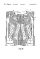
- FIG. 11 is a top perspective view of a substrate structure containing heater resistors, ink channels, and vaporization chambers, which is mounted on the back of the TAB head assembly of FIG. 4 .
- FIG. 12 is a top perspective view, partially cut away, of a portion of the TAB head assembly showing the relationship of an orifice with respect to a vaporization chamber heater resistor, and an edge of the substrate.
- FIG. 13 is a schematic cross-sectional view taken along line B—B of FIG. 10 showing the adhesive seal between the TAB head assembly and the print cartridge as well as the ink flow path around the edges of the substrate.
- FIG. 14 is a view of one arrangement of orifices and the associated heater resistors on a printhead.
- FIG. 15 is a schematic diagram of one heater resistor and its associated address line, drive transistor, primitive select line and ground line.
- FIG. 16 is a schematic diagram of the firing sequence for the address select lines when the printer carriage is moving from left to right.
- FIG. 17 is a diagram showing the layout of the contact pads on the TAB head assemble.
- FIG. 18 is a magnified perspective view showing a THA mounted on a print cartridge.
- FIG. 19 shows one end of a substrate with firing resistors #1 and #2, with the interconnects identified.
- FIG. 20 shows the opposite end of the substrate of FIG. 19, with firing resistors #299 and #300, with the interconnects identified.
- FIG. 21 shows the substrate schematics and data taken in a direction along the width of the substrate.
- FIG. 22 shows the substrate schematics and data taken in a direction along the length of the substrate.
- FIG. 23 shows a silicon wafer prior to the individual dies being cut and separated from the wafer.
- FIG. 24 shows the schematic and data for cutting a silicon wafer into individual dies.
- FIG. 25 shows a typical inkjet printer which can incorporate the printhead of the present invention
- FIG. 26 shows a carriage having removable multi-color print cartridges, which can incorporated the printhead of the present invention
- FIG. 27 is a fragmentary view of the flex-circuit interconnect on a carriage with the interior carriage walls cut away;
- FIG. 28 is a schematic block diagram of the presently preferred printer embodiment of the invention.
- a barrier layer containing ink channels and vaporization chambers is located between a rectangular substrate and a nozzle member containing an array of orifices.
- the substrate contains two linear arrays of heater elements, and each orifice in the nozzle member is associated with a vaporization chamber and heater element.
- the ink channels in the barrier layer have ink entrances generally running along two opposite edges of the substrate so that ink flowing around the edges of the substrate gain access to the ink channels and to the vaporization chambers. Piezoelectric elements can be used instead of heater elements.
- the features of the invention include an ink delivery system for an array of nozzle orifices in a print cartridge comprising an ink reservoir; a substrate having a plurality of individual ink firing chambers with an ink firing element in each chamber; an ink channel connecting said reservoir with said ink firing chambers, said channel including a primary channel connected at a first end with said reservoir and at a second end to a secondary channel; a separate inlet passage for each firing chamber connecting said secondary channel with said firing chamber for allowing high frequency refill of the firing chamber; a group of said firing chambers in adjacent relationship forming a primitive in which only one firing chamber in said primitive is activated at a time; first circuit means on said substrate connected to said firing elements; and second circuit means on said cartridge connected to said first circuit means, for transmitting firing signals to said ink firing elements at a frequency greater than 9 kHz.
- reference numeral 10 generally indicates an inkjet print cartridge incorporating a printhead according to one embodiment of the present invention simplified for illustrative purposes.
- the inkjet print cartridge 10 includes an ink reservoir 12 and a printhead 14 , where the printhead 14 is formed using Tape Automated Bonding (TAB).
- TAB head assembly 14 includes a nozzle member 16 comprising two parallel columns of offset holes or orifices 17 formed in a flexible polymer flexible circuit 18 by, for example, laser ablation.
- a back surface of the flexible circuit 18 includes conductive traces 36 formed thereon using a conventional photolithographic etching and/or plating process. These conductive traces 36 are terminated by large contact pads 20 designed to interconnect with a printer.
- the print cartridge 10 is designed to be installed in a printer so that the contact pads 20 , on the front surface of the flexible circuit 18 , contact printer electrodes providing externally generated energization signals to the printhead.
- Windows 22 and 24 extend through the flexible circuit 18 and are used to facilitate bonding of the other ends of the conductive traces 36 to electrodes on a silicon substrate containing heater resistors.
- the windows 22 and 24 are filled with an encapsulant to protect any underlying portion of the traces and substrate.
- the flexible circuit 18 is bent over the back edge of the print cartridge “snout” and extends approximately one half the length of the back wall 25 of the snout. This flap portion of the flexible circuit 18 is needed for the routing of conductive traces 36 which are connected to the substrate electrodes through the far end window 22 .
- the contact pads 20 are located on the flexible circuit 18 which is secured to this wall and the conductive traces 36 are routed over the bend and are connected to the substrate electrodes through the windows 22 , 24 in the flexible circuit 18 .
- FIGS. 2A, 2 B and 2 C show a front view of the TAB head assembly 14 of FIG. 1 removed from the print cartridge 10 and prior to windows 22 and 24 in the TAB head assembly 14 being filled with an encapsulant.
- TAB head assembly 14 has affixed to the back of the flexible circuit 18 a silicon substrate 28 (not shown) containing a plurality of individually energizable thin film resistors. Each resistor is located generally behind a single orifice 17 and acts as an ohmic heater when selectively energized by one or more pulses applied sequentially or simultaneously to one or more of the contact pads 20 .
- the orifices 17 and conductive traces 36 may be of any size, number, and pattern, and the various figures are designed to simply and clearly show the features of the invention. The relative dimensions of the various features have been greatly adjusted for the sake of clarity.
- the orifice 17 pattern on the flexible circuit 18 shown in FIG. 2 may be formed by a masking process in combination with a laser or other etching means in a step-and-repeat process, which would be readily understood by one of ordinary skilled in the art after reading this disclosure.
- FIG. 14, to be described in detail later, provides additional details of this process. Further details regarding TAB head assembly 14 and flexible circuit 18 are provided below.
- FIG. 3 is a perspective view of a simplified schematic of the inkjet print cartridge of FIG. 1 for illustrative purposes.
- FIG. 4 is a perspective view of the front surface of the Tape Automated Bonding (TAB) printhead assembly (hereinafter “TAB head assembly”) removed from the simplified schematic print cartridge of FIG. 3 .
- TAB Tape Automated Bonding
- FIG. 5 shows the back surface of the TAB head assembly 14 of FIG. 4 showing the silicon die or substrate 28 mounted to the back of the flexible circuit 18 and also showing one edge of the barrier layer 30 formed on the substrate 28 containing ink channels and vaporization chambers.
- FIG. 7 shows greater detail of this barrier layer 30 and will be discussed later. Shown along the edge of the barrier layer 30 are the entrances to the ink channels 32 which receive ink from the ink reservoir 12 .
- the conductive traces 36 formed on the back of the flexible circuit 18 terminate in contact pads 20 (shown in FIG. 4) on the opposite side of the flexible circuit 18 .
- the windows 22 and 24 allow access to the ends of the conductive traces 36 and the substrate electrodes 40 (shown in FIG. 6) from the other side of the flexible circuit 18 to facilitate bonding.
- FIG. 6 shows a side view cross-section taken along line A—A in FIG. 5 illustrating the connection of the ends of the conductive traces 36 to the electrodes 40 formed on the substrate 28 .
- a portion 42 of the barrier layer 30 is used to insulate the ends of the conductive traces 36 from the substrate 28 .
- Also shown in FIG. 6 is a side view of the flexible circuit 18 , the barrier layer 30 , the windows 22 and 24 , and the entrances of the various ink channels 32 . Droplets of ink 46 are shown being ejected from orifice holes associated with each of the ink channels 32 .
- FIG. 7 shows the print cartridge 10 of FIG. 1 with the TAB head assembly 14 removed to reveal the headland pattern 50 used in providing a seal between the TAB head assembly 14 and the printhead body.
- FIG. 8 shows the headland area in enlarged perspective view.
- FIG. 9 shows the headland area in an enlarged top plan view. The headland characteristics are exaggerated for clarity. Shown in FIGS. 8 and 9 is a central slot 52 in the print cartridge 10 for allowing ink from the ink reservoir 12 to flow to the back surface of the TAB head assembly 14 .
- the headland pattern 50 formed on the print cartridge 10 is configured so that a bead of epoxy adhesive (not shown) dispensed on the inner raised walls 54 and across the wall openings 55 and 56 (so as to circumscribe the substrate when the TAB head assembly 14 is in place) will form an ink seal between the body of the print cartridge 10 and the back of the TAB head assembly 14 when the TAB head assembly 14 is pressed into place against the headland pattern 50 .
- Other adhesives which may be used include hot-melt, silicone, UV curable adhesive, and mixtures thereof.
- a patterned adhesive film may be positioned on the headland, as opposed to dispensing a bead of adhesive.
- the TAB head assembly 14 of FIG. 5 When the TAB head assembly 14 of FIG. 5 is properly positioned and pressed down on the headland pattern 50 in FIG. 8 after the adhesive (not shown) is dispensed, the two short ends of the substrate 28 will be supported by the surface portions 57 and 58 within the wall openings 55 arid 56 . Additional details regarding adhesive 90 are shown in FIG. 13 .
- the configuration of the headland pattern 50 is such that, when the substrate 28 is supported by the surface portions 57 and 58 and adjoining central peninsulas 57 a and 58 a, the back surface of the flexible circuit 18 will be slightly above the top of the raised walls 54 and approximately flush with the flat top surface 59 of the print cartridge 10 .
- the adhesive is squished down. From the top of the inner raised walls 54 , the adhesive overspills into the gutter or groove 53 between the inner raised walls 54 and the outer raised wall 60 and overspills somewhat toward the slot 52 . From the wall openings 55 and 56 , the adhesive squishes inwardly in the direction of slot 52 and squishes outwardly toward the outer raised wall 60 , which blocks further outward displacement of the adhesive.
- the outward displacement of the adhesive not only serves as an ink seal, but encapsulates the conductive traces in the vicinity of the headland 50 from underneath to protect the traces from ink.
- FIG. 10 shows a portion of the completed print cartridge 10 of FIG. 3 illustrating, by cross-hatching, the location of the underlying adhesive 90 (not shown) which forms the seal between the TAB head assembly 14 and the body of the print cartridge 10 .
- the adhesive is located generally between the dashed lines surrounding the array of orifices 17 , where the outer dashed line 62 is slightly within the boundaries of the outer raised wall 60 in FIG. 7, and the inner dashed line 64 is slightly within the boundaries of the inner raised walls 54 in FIG. 7 .
- the adhesive is also shown being squished through the wall openings 55 and 56 (FIG. 7) to encapsulate the traces leading to electrodes on the substrate. A cross-section of this seal taken along line B—B in FIG. 10 is also shown in FIG. 13, to be discussed later.
- This seal formed by the adhesive 90 circumscribing the substrate 28 allows ink to flow from slot 52 and around the sides of the substrate to the vaporization chambers formed in the barrier layer 30 , but will prevent ink from seeping out from under the TAB head assembly 14 .
- this adhesive seal 90 provides a strong mechanical coupling of the TAB head assembly 14 to the print cartridge 10 , provides a fluidic seal, and provides trace encapsulation.
- the adhesive seal is also easier to cure than prior art seals, and it is much easier to detect leaks between the print cartridge body and the printhead, since the sealant line is readily observable. Further details on adhesive seal 90 are shown in FIG. 13 .
- FIG. 11 is a front perspective view of the silicon substrate 28 which is affixed to the back of the flexible circuit 18 in FIG. 5 to form the TAB head assembly 14 .
- Silicon substrate 28 has formed on it, using conventional photolithographic techniques, two rows or columns of thin film resistors 70 , shown in FIG. 11 exposed through the vaporization chambers 72 formed in the barrier layer 30 .
- the substrate 28 is approximately one-half inch long and contains 300 heater resistors 70 , thus enabling a resolution of 600 dots per inch.
- Heater resistors 70 may instead be any other type of ink ejection element, such as a piezoelectric pump-type element or any other conventional element.
- element 70 in all the various figures may be considered to be piezoelectric elements in an alternative embodiment without affecting the operation of the printhead.
- electrodes 74 are also formed on the substrate 28 for connection to the conductive traces 36 (shown by dashed lines) formed on the back of the flexible circuit 18 .
- a demultiplexer 78 shown by a dashed outline in FIG. 11, is also formed on the substrate 28 for demultiplexing the incoming multiplexed signals applied to the electrodes 74 and distributing the signals to the various thin film resistors 70 .
- the demultiplexer 78 enables the use of much fewer electrodes 74 than thin film resistors 70 . Having fewer electrodes allows all connections to the substrate to be made from the short end portions of the substrate, as shown in FIG. 4, so that these connections will not interfere with the ink flow around the long sides of the substrate.
- the demultiplexer 78 may be any decoder for decoding encoded signals applied to the electrodes 74 .
- the demultiplexer has input leads (not shown for simplicity) connected to the electrodes 74 and has output leads (not shown) connected to the various resistors 70 .
- the demultiplexer 78 circuity is discussed in further detail below.
- barrier layer 30 is also formed on the surface of the substrate 28 using conventional photolithographic techniques, which is formed the vaporization chambers 72 and ink channels 80 .
- a portion 42 of the barrier layer 30 insulates the conductive traces 36 from the underlying substrate 28 , as previously discussed with respect to FIG. 4 .
- a thin adhesive layer 84 (not shown), such as an uncured layer of poly-isoprene photoresist, is applied to the top surface of the barrier layer 30 .
- a separate adhesive layer may not be necessary if the top of the barrier layer 30 can be otherwise made adhesive.
- the resulting substrate structure is then positioned with respect to the back surface of the flexible circuit 18 so as to align the resistors 70 with the orifices formed in the flexible circuit 18 . This alignment step also inherently aligns the electrodes 74 with the ends of the conductive traces 36 . The traces 36 are then bonded to the electrodes 74 .
- the aligned and bonded substrate/flexible circuit structure is then heated while applying pressure to cure the adhesive layer 84 and firmly affix the substrate structure to the back surface of the flexible circuit 18 .
- FIG. 12 is an enlarged view of a single vaporization chamber 72 , thin film resistor 70 , and frustum shaped orifice 17 after the substrate structure of FIG. 11 is secured to the back of the flexible circuit 18 via the thin adhesive layer 84 .
- a side edge of the substrate 28 is shown as edge 86 .
- ink flows from the ink reservoir 12 around the side edge 86 of the substrate 28 , and into the ink channel 80 and associated vaporization chamber 72 , as shown by the arrow 88 .
- a thin layer of the adjacent ink is superheated, causing explosive vaporization and, consequently, causing a droplet of ink to be ejected through the orifice 17 .
- the vaporization chamber 72 is then refilled by capillary action.
- the barrier layer 30 is approximately 1 mils thick, the substrate 28 is approximately 20 mils thick, and the flexible circuit 18 is approximately 2 mils thick.
- FIG. 13 Shown in FIG. 13 is a side elevational view cross-section taken along line B—B in FIG. 10 showing a portion of the adhesive seal 90 , applied to the inner raised wall 54 and wall openings 55 , 56 , surrounding the substrate 28 and showing the substrate 28 being adhesively secured to a central portion of the flexible circuit 18 by the thin adhesive layer 84 on the top surface of the barrier layer 30 containing the ink channels and vaporization chambers 92 and 94 .
- a portion of the plastic body of the printhead cartridge 10 including raised walls 54 shown in FIGS. 7 and 8, is also shown.
- FIG. 13 also illustrates how ink 88 from the ink reservoir 12 flows through the central slot 52 formed in the print cartridge 10 and flows around the edges 86 of the substrate 28 through ink channels 80 into the vaporization chambers 92 and 94 .
- Thin film resistors 96 and 98 are shown within the vaporization chambers 92 and 94 , respectively. When the resistors 96 and 98 are energized, the ink within the vaporization chambers 92 and 94 are ejected, as illustrated by the emitted drops of ink 101 and 102 .
- the edge feed feature where ink flows around the edges 86 of the substrate 28 and directly into ink channels 80 , has a number of advantages over previous center feed printhead designs which form an elongated central hole or slot running lengthwise in the substrate to allow ink to flow into a central manifold and ultimately to the entrances of ink channels.
- One advantage is that the substrate or die 28 width can be made narrower, due to the absence of the elongated central hole or slot in a central interior portion 29 of the substrate. Not only can the substrate be made narrower, but the length of the edge feed substrate can be shorter, for the same number of nozzles, than the center feed substrate due to the substrate structure now being less prone to cracking or breaking without the central ink feed hole.
- This shortening of a substrate die 210 (see FIG. 23) to form the substrate 28 enables a shorter headland 50 in FIG. 8 and, hence, a shorter print cartridge snout.
- the star wheels can be located closer to the pinch rollers to ensure better paper/roller contact along the transport path of the print cartridge snout. Additionally, by making the substrate smaller, more substrates can be formed per wafer, thus lowering the material cost per substrate.
- edge feed feature manufacturing time is saved by not having to etch a slot in the substrate, and the substrate is less prone to breakage during handling. Further, the substrate is able to dissipate more heat, since the ink flowing across the back of the substrate and around the edges of the substrate acts to draw heat away from the back of the substrate.
- the edge feed design Be eliminating the manifold as well as the slot in the substrate, the ink is able to flow more rapidly into the vaporization chambers, since there is less restriction on the ink flow. This more rapid ink flow improves the frequency response of the printhead, allowing higher printing rates from a given number of orifices. Further, the more rapid ink flow reduces crosstalk between nearby vaporization chambers caused by variations in ink flow as the heater elements in the vaporization chambers are fired.
- the ink reservoir contains two separate ink sources, each containing a different color of ink.
- the central slot 52 in FIG. 13 is bisected, as shown by the dashed line 103 , so that each side of the central slot 52 communicates with a separate ink source. Therefore, the left linear array of vaporization chambers can be made to eject one color of ink, while the right linear array of vaporization chambers can be made to eject a different color of ink.
- This concept can even be used to create a four color printhead, where a different ink reservoir feeds ink to ink channels along each of the four sides of the substrate.
- a four-edge design would be used, preferably using a square substrate for symmetry.
- the TAB head assembly is positioned on the print cartridge 10 , and the previously described adhesive seal 90 is formed to firmly secure the nozzle member to the print cartridge, provide an ink-proof seal around the substrate between the nozzle member and the ink reservoir, and encapsulate the traces in the vicinity of the headland so as to isolate the traces from the ink.
- Peripheral points on the flexible TAB head assembly are then secured to the plastic print cartridge 10 by a conventional melt-through type bonding process to cause the polymer flexible circuit 18 to remain relatively flush with the surface of the print cartridge 10 , as shown in FIG. 1 .
- the printhead nozzles must be placed closer together. This requires that both heater resistors and the associated orifices be placed closer together.
- the orifices 17 in the nozzle member 16 of the TAB head assembly are generally arranged in two major columns of orifices 17 as shown in FIG. 14 .
- the orifices 17 are conventionally assigned a number as shown, starting at the top right as the TAB head assembly as viewed from the external surface of the nozzle member 16 and ending in the lower left, thereby resulting in the odd numbers being arranged in one column and even numbers being arranged in the second column.
- the orifices/resistors in each column are spaced ⁇ fraction (1/300) ⁇ of an inch apart in the long direction of the nozzle member.
- the orifices and resistors in one column are offset from the orifice/resistors in the other column in the long direction of the nozzle member by ⁇ fraction (1/600) ⁇ of an inch, thus, providing 600 dots per inch (dpi) printing.
- the orifices 17 while aligned in two major columns as described, are further arranged in an offset pattern within each column to match the offset heater resistors 70 disposed in the substrate 28 as illustrated in FIG. 14 .
- a small offset E is provided between resistors. This small offset E allows adjacent resistors 70 to be fired at slightly different times when the TAB head assembly is scanning across the recording medium to further minimize cross-talk effects between adjacent vaporization chambers 130 .
- the resistors are fired at twenty two different times, the offset allows the ejected ink drops from different nozzles to be placed in the same horizontal position on the print media.
- the resistors 70 are coupled to electrical drive circuitry (not shown in FIG.
- the firing heater resistors 70 of the preferred embodiment are organized as fourteen primitive groups of twenty or twenty-two resistors. It can be seen that each resistor (numbered 1 through 300 and corresponding to the orifices 17 of FIG. 14) is controlled by its own FET drive transistor, which shares its control input Address Select (A 1 -A 22 ) with thirteen other resistors. Each resistor is tied to nineteen or twenty-one other resistors by a common node Primitive Select (PS 1 -PS 14 ). Consequently, firing a particular resistor requires applying a control voltage at its “Address Select” terminal and an electrical power source at its “Primitive Select” terminal. Only one Address Select line is enabled at one time.
- FIG. 15 is a schematic diagram of an individual heater resistor and its FET drive transistor. As shown in FIG. 15, Address Select and Primitive Select lines also contain transistors for draining unwanted electrostatic discharge and pull down resistors to place all unselected addresses in an off state. Table I shows the correlation between the firing resistor/orifice and the Address Select and Primitive Select Lines.
- the Address Select lines are sequentially turned on via TAB head assembly interface circuitry according to a firing order counter located in the printer and sequenced (independently of the data directing which resistor is to be energized) from A 1 to A 22 when printing form left to right and from A 22 to A 1 when printing from right to left.
- the print data retrieved from the printer memory turns on any combination of the Primitive Select lines.
- Primitive Select lines (instead of Address Select lines) are used in the preferred embodiment to control the pulse width. Disabling Address Select lines while the drive transistors are conducting high current can cause avalanche breakdown and consequent physical damage to MOS transistors. Accordingly, the Address Select lines are “set” before power is applied to the Primitive Select lines, and conversely, power is turned off before the Address Select lines are changed.
- each primitive is selectively fired by powering the associated primitive select interconnection.
- To provide uniform energy per heater resistor only one resistor is energized at a time per primitive.
- any number of the primitive selects may be enabled concurrently.
- Each enabled primitive select thus delivers both power and one of the enable signals to the driver transistor.
- the other enable signal is an address signal provided by each address select line only one of which is active at a time.
- Each address select line is tied to all of the switching transistors so that all such switching devices are conductive when the interconnection is enabled. Where a primitive select interconnection and an address select line for a heater resistor are both active simultaneously, that particular heater resistor is energized.
- FIG. 16 shows the firing sequence when the print carriage is scanning from left to right. The firing sequence is reversed when scanning from right to left.
- the resistor firing frequency is shown as F in FIG. 16. A brief rest period of approximately ten percent of the period, 1/F is allowed between cycles. This rest period prevents Address Select cycles from overlapping due to printer carriage velocity variations.
- the interconnections for controlling the TAB head assembly driver circuitry include separate primitive select and primitive common interconnections.
- the driver circuity of the preferred embodiment comprises an array of fourteen primitives, fourteen primitive commons, and twenty-two address select lines, thus requiring 50 interconnections to control 300 firing resistors.
- the integration of both heater resistors and FET driver transistors onto a common substrate creates the need for additional layers of conductive circuitry on the substrate so that the transistors could be electrically connected to the resistors and other components of the system. This creates a concentration of heat generation within the substrate.
- the print cartridge 10 is designed to be installed in a printer so that the contact pads 20 , on the front surface of the flexible circuit 18 , contact printer electrodes which couple externally generated energization signals to the TAB head assembly.
- To access the traces 36 on the back surface of the flexible circuit 18 from the front surface of the flexible circuit holes (vias) are formed through the front surface of the flexible circuit to expose the ends of the traces.
- the exposed ends of the traces are then plated with, for example, gold to form the contact pads 20 shown on the front surface of the flexible circuit in FIG. 2 .
- the contact or interface pads 20 are assigned the functions listed in Table II.
- FIG. 17 shows the location of the interface pads 20 on the TAB head assembly of FIG. 2 .
- FIG. 18 shows the relative positions of the even # nozzles 2 through 300 and the odd # nozzles 1 through 299 when the THA is mounted on a print cartridge.
- FIGS. 19-20 are an enlarged illustration of both truncated end portions 202 , 204 of the substrate showing the ESD devices 206 and the interconnect junctions 208 .
- FIGS. 21-22 includes schematic drawings as well as related data tables showing the dimensions, electrical resistance and identification of the various circuitry portions of the substrate. It will be appreciated by those skilled in the art that substantial heat is generated by all of the circuitry on the substrate. More particularly, each firing resistor requires 300 milliamps whenever it is selected for firing. For a 12 KHertz firing frequency of F, and in reference to the firing diagram of FIG. 16, when all of the twenty-two address lines are activated in a duty cycle with each pulse width being 2.3 microseconds, then 2.3 ⁇ 22 equals a result divided by 83 microseconds to create a 61% duty cycle. Therefore it is possible when all primitives are firing at the same time to pass a current of approximately 25 amps through the substrate (300 milliamps ⁇ 14 ⁇ 0.61). The cooling characteristices of the edge feed design are therefore very helpful in avoiding the overheating of the substrate during normal operation.
- FIGS. 23-24 show the dimensions for cutting a silicon wafer in order to obtain a high yield for the substrate dies of the present invention.
- some of the dies such as 210 which extend into the 5 mm wide exclusion zone 212 are not usable if critical components of the multilayer substrate lie inside such exclusion zone, nevertheless the invention still provides significantly better yield than for an estimated yield for a center feed ink channel design having the same 300 nozzle 600 dpi specifications as the presently preferred embodiment of the present invention.
- a 600 dpi 1 ⁇ 2 inch swath black pen with three 300 dpi color pens each generating a swath of approximately 1 ⁇ 3 inch.
- the high performance black pen is typically used for printing text and other “black only” features, and thus the output quality and throughput of these features is greater. It also improves the output quality of color graphics and color features by teaming with the three lower performance color pens when printing color graphics or color features.
- the black component of the graphics which is often a large portion of color graphics content is at a higher resolution and thus at a higher output quality level.
- the larger swath can then be combined with printing algorithms to improve the throughput of color graphics.
- inkjet printer 110 includes an input tray 112 containing sheets of media 114 which pass through a print zone, and are fed past an exit 118 into an output tray 116 .
- a movable carriage 120 holds print cartridges 122 , 124 , 126 , and 128 which respectively hold yellow (Y), magenta (M), cyan (C) and black (K) inks.
- the front of the carriage has a support bumper 130 which rides along a guide 132 while the back of the carriage has multiple bushings such as 34 which ride along slide rod 136 .
- the position of the carriage as it traverses back and forth across the media is determined from an encoder strip 138 in order to be sure that the various ink nozzles on each print cartridge are selectively fired at the appropriate time during a carriage scan.
- a 300 dpi color inkjet cartridge 140 having a tab-circuit with a four column thirty-two pad electrical interconnect 142 is removably installed in three chutes 144 , 146 , 148 of a unitary carriage 150 .
- a flex-circuit member 52 having three matching sets of conductive pads 54 , 56 , 58 is mounted on flex-frame pins 160 for operative engagement with the cartridge pads when the cartridge is inserted into its appropriate chute.
- An enlarged set of conductive pads 162 covering a larger area, having a different layout, and constituting an array of six columns totaling fifty-two conductive pads on the flex-circuit member is designed for operative engagement with cartridge pads on a 600 dpi black injet cartridge 164 .
- FIG. 28 shows the preferred mounting relationship between a 300 dpi nozzle array 196 of the color printheads and a 600 dpi nozzle array 198 of the black printhead.
- Control circuitry 199 on the substrate enables the three hundred firing resistors of the black printhead to be controlled through fifty-two electrical interconnect jpads, and similary enables all one hundred four firing resistors of each color printhead to be controlled through thirty-two electrical interconnect pads.
- This invention allows higher resolution and speed to occur for frequently printed features such as text and the most frequent color components of graphics such as black.
- the entire page is faster and of higher quality and is more comprable with laser printing performance (8+pages per minute) and laser printing quality (600 dpi resolution).
Abstract
Description
| TABLE I |
| Nozzle Number by Address Select and Primitive Select Lines |
| P1 | P2 | P3 | P4 | P5 | P6 | P7 | P8 | P9 | P10 | P11 | P12 | P13 | P14 | ||
| A1 | 1 | 45 | 42 | 89 | 86 | 133 | 130 | 177 | 174 | 221 | 21B | 265 | 262 | |
| A2 | 7 | 4 | 51 | 48 | 95 | 92 | 139 | 136 | 183 | 180 | 227 | 224 | 271 | 268 |
| A3 | 13 | 10 | 57 | 54 | 101 | 98 | 145 | 142 | 129 | 186 | 233 | 230 | 277 | 274 |
| A4 | 19 | 16 | 63 | 60 | 107 | 104 | 151 | 148 | 195 | 192 | 239 | 236 | 283 | 280 |
| A5 | 25 | 22 | 63 | 66 | 113 | 110 | 157 | 154 | 201 | 198 | 245 | 242 | 289 | 286 |
| A6 | 31 | 28 | 75 | 72 | 119 | 118 | 163 | 160 | 207 | 204 | 251 | 248 | 295 | 292 |
| A7 | 37 | 34 | 81 | 78 | 125 | 122 | 169 | 166 | 213 | 204 | 257 | 254 | 298 | |
| A8 | 40 | 43 | 84 | 87 | 125 | 131 | 172 | 175 | 216 | 219 | 260 | 263 | ||
| A9 | 5 | 2 | 49 | 46 | 93 | 90 | 137 | 134 | 181 | 178 | 225 | 222 | 269 | 266 |
| A10 | 11 | 8 | 55 | 52 | 99 | 96 | 143 | 140 | 187 | 184 | 231 | 228 | 275 | 272 |
| A11 | 17 | 14 | 61 | 58 | 105 | 102 | 149 | 146 | 193 | 190 | 237 | 234 | 281 | 278 |
| A12 | 23 | 20 | 67 | 64 | 111 | 108 | 155 | 152 | 199 | 196 | 243 | 240 | 287 | 284 |
| A13 | 29 | 26 | 73 | 70 | 117 | 114 | 161 | 158 | 205 | 202 | 249 | 246 | 293 | 290 |
| A14 | 35 | 32 | 79 | 76 | 123 | 120 | 167 | 164 | 211 | 208 | 255 | 252 | 299 | 296 |
| A15 | 38 | 41 | 82 | 85 | 126 | 129 | 170 | 173 | 214 | 217 | 258 | 261 | ||
| A16 | 3 | 47 | 44 | 91 | 88 | 135 | 132 | 179 | 176 | 223 | 220 | 267 | 264 | |
| A17 | 9 | 6 | 53 | 50 | 97 | 94 | 141 | 138 | 185 | 182 | 229 | 226 | 273 | 270 |
| A18 | 15 | 12 | 59 | 56 | 103 | 100 | 147 | 144 | 191 | 188 | 235 | 232 | 279 | 276 |
| A19 | 21 | 18 | 65 | 62 | 109 | 106 | 153 | 150 | 197 | 194 | 241 | 238 | 285 | 282 |
| A20 | 27 | 24 | 71 | 68 | 115 | 112 | 159 | 156 | 203 | 200 | 247 | 244 | 291 | 288 |
| A21 | 33 | 30 | 77 | 74 | 121 | 118 | 165 | 162 | 209 | 206 | 253 | 250 | 297 | 294 |
| A22 | 39 | 36 | 83 | 80 | 127 | 124 | 171 | 168 | 215 | 212 | 259 | 256 | 300 | |
| TABLE 11 |
| ELECTRICAL PAD DEFINITON |
| Odd Side of Head | Even Side of Head |
| Pad# | Name | Function | Pad# | Name | Function |
| 1 | A9 | Address Select 9 | 2 | G6 | Common 6 |
| 3 | PS7 | Primitive Select 7 | 4 | PS6 | Primitive Select 6 |
| 5 | G7 | Common 7 | 6 | A11 | Address Select 11 |
| 7 | PS5 | Primitive Select 5 | 8 | A13 | Address Select 13 |
| 9 | G5 | Common 5 | 10 | G4 | Common 4 |
| 11 | G3 | Common 3 | 12 | PS4 | Primitive Select 4 |
| 13 | PS3 | Primitive Select 3 | 14 | A15 | Address Select 15 |
| 15 | A7 | Address Select 7 | 16 | A17 | Address Select 17 |
| 17 | A5 | Address Select 5 | 18 | G2 | Common 2 |
| 19 | G1 | Common 1 | 20 | PS2 | Primitive Select 2 |
| 21 | PS1 | Primitive Select 1 | 22 | A19 | Address Select 19 |
| 23 | A3 | Address Select 3 | 24 | A21 | Address Select 21 |
| 25 | A1 | Address Select 1 | 26 | A22 | Address Select 22 |
| 27 | TSR | Thermal Sense | 28 | R10X | 10X Resistor |
| 29 | A2 | Address Select 2 | 30 | A20 | Address Select 20 |
| 31 | A4 | Address Select 4 | 32 | PS14 | Primitive Select 14 |
| 33 | PS13 | Primitive Select 13 | 34 | G14 | Common 14 |
| 35 | G13 | Common 13 | 36 | A18 | Address Select 18 |
| 37 | A6 | Address Select 6 | 38 | A16 | Address Select 16 |
| 39 | A8 | Address Select 8 | 40 | PS12 | Primitive Select 12 |
| 41 | PS11 | Primitive Select 11 | 42 | G12 | Common 12 |
| 43 | G11 | Common 11 | 44 | G10 | Common 10 |
| 45 | A10 | Address Select 10 | 46 | PS10 | Primitive Select 10 |
| 47 | A12 | Address Select 12 | 48 | G8 | Common 8 |
| 49 | PS9 | Primitive Select 9 | 50 | P58 | Primitive Select 8 |
| 51 | G9 | Common 9 | 52 | A14 | Address Select 14 |
Claims (17)
Priority Applications (1)
| Application Number | Priority Date | Filing Date | Title |
|---|---|---|---|
| US09/395,379 US6332677B1 (en) | 1992-04-02 | 1999-09-14 | Stable substrate structure for a wide swath nozzle array in a high resolution inkjet printer |
Applications Claiming Priority (6)
| Application Number | Priority Date | Filing Date | Title |
|---|---|---|---|
| US07/862,086 US5278584A (en) | 1992-04-02 | 1992-04-02 | Ink delivery system for an inkjet printhead |
| US08/145,261 US5949453A (en) | 1993-10-29 | 1993-10-29 | Mixed resolution printing for color and monochrome printers |
| US08/179,866 US5625396A (en) | 1992-04-02 | 1994-01-11 | Ink delivery method for an inkjet print cartridge |
| US08/319,894 US5648806A (en) | 1992-04-02 | 1994-10-06 | Stable substrate structure for a wide swath nozzle array in a high resolution inkjet printer |
| US08/893,775 US5984464A (en) | 1992-04-02 | 1997-07-11 | Stable substrate structure for a wide swath nozzle array in a high resolution inkjet printer |
| US09/395,379 US6332677B1 (en) | 1992-04-02 | 1999-09-14 | Stable substrate structure for a wide swath nozzle array in a high resolution inkjet printer |
Related Parent Applications (1)
| Application Number | Title | Priority Date | Filing Date |
|---|---|---|---|
| US08/893,775 Continuation US5984464A (en) | 1992-04-02 | 1997-07-11 | Stable substrate structure for a wide swath nozzle array in a high resolution inkjet printer |
Publications (1)
| Publication Number | Publication Date |
|---|---|
| US6332677B1 true US6332677B1 (en) | 2001-12-25 |
Family
ID=23244052
Family Applications (3)
| Application Number | Title | Priority Date | Filing Date |
|---|---|---|---|
| US08/319,894 Expired - Lifetime US5648806A (en) | 1992-04-02 | 1994-10-06 | Stable substrate structure for a wide swath nozzle array in a high resolution inkjet printer |
| US08/893,775 Expired - Lifetime US5984464A (en) | 1992-04-02 | 1997-07-11 | Stable substrate structure for a wide swath nozzle array in a high resolution inkjet printer |
| US09/395,379 Expired - Fee Related US6332677B1 (en) | 1992-04-02 | 1999-09-14 | Stable substrate structure for a wide swath nozzle array in a high resolution inkjet printer |
Family Applications Before (2)
| Application Number | Title | Priority Date | Filing Date |
|---|---|---|---|
| US08/319,894 Expired - Lifetime US5648806A (en) | 1992-04-02 | 1994-10-06 | Stable substrate structure for a wide swath nozzle array in a high resolution inkjet printer |
| US08/893,775 Expired - Lifetime US5984464A (en) | 1992-04-02 | 1997-07-11 | Stable substrate structure for a wide swath nozzle array in a high resolution inkjet printer |
Country Status (3)
| Country | Link |
|---|---|
| US (3) | US5648806A (en) |
| EP (1) | EP0707967B1 (en) |
| DE (1) | DE69509853T2 (en) |
Cited By (28)
| Publication number | Priority date | Publication date | Assignee | Title |
|---|---|---|---|---|
| EP1473161A1 (en) * | 2003-04-22 | 2004-11-03 | Microjet Technology Co., Ltd | Assembling structure of printhead |
| US20050128254A1 (en) * | 2003-12-16 | 2005-06-16 | Canon Kabushiki Kaisha | Substrate for liquid discharge head, liquid discharge head using substrate for liquid discharge head and method of manufacturing the same |
| US20060008307A1 (en) * | 2000-05-23 | 2006-01-12 | Silverbrook Research Pty Ltd | Print engine assembly with an elongate converging ink distribution assembly |
| US20060007280A1 (en) * | 2004-07-08 | 2006-01-12 | Ang Kian H | Ink cartridge component |
| US20060007276A1 (en) * | 2000-05-23 | 2006-01-12 | Silverbrook Research Pty Ltd | Ink distribution structure for a printhead |
| US20060279784A1 (en) * | 2005-06-10 | 2006-12-14 | Carlson Gregory F | Handheld printer |
| CN1301860C (en) * | 2003-09-10 | 2007-02-28 | 研能科技股份有限公司 | Packaging structure and packaging method for ink feeding passage of ink-jetting head |
| US20070080494A1 (en) * | 2005-10-11 | 2007-04-12 | Marshall Jerry A Jr | Media transport system |
| CN1313273C (en) * | 2003-04-22 | 2007-05-02 | 研能科技股份有限公司 | Method for encapsulating ink gun |
| US20070109388A1 (en) * | 2000-09-15 | 2007-05-17 | Silverbrook Research Pty Ltd | Ink jet printer with a belt-loading mechanism |
| CN1330492C (en) * | 2003-04-22 | 2007-08-08 | 研能科技股份有限公司 | Structure of ink gun and ink jet printing system |
| US7278720B2 (en) | 2005-01-24 | 2007-10-09 | Hewlett-Packard Develpoment Company, L.P. | Ink cartridge with multiple chambers aligned along an axial length |
| US20080079779A1 (en) * | 2006-09-28 | 2008-04-03 | Robert Lee Cornell | Method for Improving Thermal Conductivity in Micro-Fluid Ejection Heads |
| US20080215286A1 (en) * | 2007-03-02 | 2008-09-04 | Mealy James | Apparatus and method for determining the position of a device |
| US20080211864A1 (en) * | 2007-03-02 | 2008-09-04 | Mealy James | Device and method for servicing an inkjet print head on a hand held printer |
| US20100184244A1 (en) * | 2009-01-20 | 2010-07-22 | SunPrint, Inc. | Systems and methods for depositing patterned materials for solar panel production |
| US20100277538A1 (en) * | 2000-05-24 | 2010-11-04 | Silverbrook Research Pty Ltd | Print engine assembly with twin bearing moldings received within chassis |
| US20110057989A1 (en) * | 2000-05-24 | 2011-03-10 | Silverbrook Research Pty Ltd | Inkjet printing device having rotating platen |
| US8077350B1 (en) | 2008-04-18 | 2011-12-13 | Marvell International Ltd. | Device and method for dispensing white ink |
| US8079765B1 (en) | 2007-03-02 | 2011-12-20 | Marvell International Ltd. | Hand-propelled labeling printer |
| US8096713B1 (en) | 2007-03-02 | 2012-01-17 | Marvell International Ltd. | Managing project information with a hand-propelled device |
| US8107108B1 (en) * | 2007-02-28 | 2012-01-31 | Marvell International Ltd. | Providing user feedback in handheld device |
| US8128192B1 (en) | 2007-02-28 | 2012-03-06 | Marvell International Ltd. | Cap design for an inkjet print head with hand-held imaging element arrangement with integrated cleaning mechanism |
| US20120127239A1 (en) * | 2010-11-19 | 2012-05-24 | Seiko Epson Corporation | Circuit substrate |
| US8705117B1 (en) | 2007-06-18 | 2014-04-22 | Marvell International Ltd. | Hand-held printing device and method for tuning ink jet color for printing on colored paper |
| US8827442B1 (en) | 2007-02-23 | 2014-09-09 | Marvell International Ltd. | Print head configuration for hand-held printing |
| US10259230B2 (en) | 2005-12-26 | 2019-04-16 | Seiko Epson Corporation | Printing material container, and board mounted on printing material container |
| US11034147B2 (en) | 2017-04-14 | 2021-06-15 | Hewlett-Packard Development Company, L.P. | Fluidic die |
Families Citing this family (56)
| Publication number | Priority date | Publication date | Assignee | Title |
|---|---|---|---|---|
| US5648806A (en) * | 1992-04-02 | 1997-07-15 | Hewlett-Packard Company | Stable substrate structure for a wide swath nozzle array in a high resolution inkjet printer |
| US6543884B1 (en) | 1996-02-07 | 2003-04-08 | Hewlett-Packard Company | Fully integrated thermal inkjet printhead having etched back PSG layer |
| US6336714B1 (en) | 1996-02-07 | 2002-01-08 | Hewlett-Packard Company | Fully integrated thermal inkjet printhead having thin film layer shelf |
| US6305790B1 (en) | 1996-02-07 | 2001-10-23 | Hewlett-Packard Company | Fully integrated thermal inkjet printhead having multiple ink feed holes per nozzle |
| US5719605A (en) * | 1996-11-20 | 1998-02-17 | Lexmark International, Inc. | Large array heater chips for thermal ink jet printheads |
| US5984455A (en) * | 1997-11-04 | 1999-11-16 | Lexmark International, Inc. | Ink jet printing apparatus having primary and secondary nozzles |
| US6017112A (en) * | 1997-11-04 | 2000-01-25 | Lexmark International, Inc. | Ink jet printing apparatus having a print cartridge with primary and secondary nozzles |
| US6390585B1 (en) | 1998-07-21 | 2002-05-21 | Hewlett-Packard Company | Selectively warming a printhead for optimized performance |
| US6276777B1 (en) | 1998-07-21 | 2001-08-21 | Hewlett-Packard Company | Variable maximum operating temperature for a printhead |
| US6145980A (en) * | 1998-11-24 | 2000-11-14 | Hewlett-Packard Company | Multiple-zone inkjet printer |
| US6705705B2 (en) * | 1998-12-17 | 2004-03-16 | Hewlett-Packard Development Company, L.P. | Substrate for fluid ejection devices |
| US6545773B1 (en) | 1999-03-01 | 2003-04-08 | Hewlett-Packard Company | Compensation for print-direction induced hue shift using depletion |
| US6244687B1 (en) | 1999-03-22 | 2001-06-12 | Hewlett-Packard Company | Mixing overprinting and underprinting of inks in an inkjet printer to speed up the dry time of black ink without undesirable hue shifts |
| US6186622B1 (en) | 1999-05-26 | 2001-02-13 | Hewlett-Packard Company | Low expansion snout insert for inkjet print cartridge |
| US6132021A (en) * | 1999-06-10 | 2000-10-17 | Hewlett-Packard Company | Dynamic adjustment of under and over printing levels in a printer |
| US6312112B1 (en) | 1999-07-12 | 2001-11-06 | Hewlett-Packard Company | Long life printhead architecture |
| US6190000B1 (en) | 1999-08-30 | 2001-02-20 | Hewlett-Packard Company | Method and apparatus for masking address out failures |
| US6312079B1 (en) * | 1999-09-22 | 2001-11-06 | Lexmark International, Inc. | Print head drive scheme for serial compression of I/O in ink jets |
| EP1245000B1 (en) * | 2000-01-04 | 2004-02-25 | Encad, Inc. | Print masks for high speed ink jet printing |
| US6530645B2 (en) | 2000-04-03 | 2003-03-11 | Eastman Kodak Company | Print masks for high speed ink jet printing |
| DE10117035B4 (en) | 2000-04-27 | 2006-08-17 | Hewlett-Packard Development Co., L.P., Houston | Printing technique to hide band boundary banding |
| KR100403578B1 (en) * | 2000-07-20 | 2003-11-01 | 삼성전자주식회사 | Ink jet printing head |
| CA2419017C (en) * | 2000-08-11 | 2008-06-10 | Spectra, Inc. | Ink jet printing |
| US6364466B1 (en) | 2000-11-30 | 2002-04-02 | Hewlett-Packard Company | Particle tolerant ink-feed channel structure for fully integrated inkjet printhead |
| US6857803B2 (en) | 2001-01-08 | 2005-02-22 | Vutek, Inc. | Printing system web guide with a removable platen |
| US6679640B2 (en) | 2001-01-08 | 2004-01-20 | Vutek, Incorporated | Printing system web guide coupling assembly |
| US6419346B1 (en) | 2001-01-25 | 2002-07-16 | Hewlett-Packard Company | Two-step trench etch for a fully integrated thermal inkjet printhead |
| US6755503B2 (en) | 2001-02-23 | 2004-06-29 | Mailroom Technology, Inc. | Housekeeping station |
| US6517735B2 (en) | 2001-03-15 | 2003-02-11 | Hewlett-Packard Company | Ink feed trench etch technique for a fully integrated thermal inkjet printhead |
| US6922203B2 (en) * | 2001-06-06 | 2005-07-26 | Hewlett-Packard Development Company, L.P. | Barrier/orifice design for improved printhead performance |
| US6561632B2 (en) | 2001-06-06 | 2003-05-13 | Hewlett-Packard Development Company, L.P. | Printhead with high nozzle packing density |
| US6619786B2 (en) | 2001-06-08 | 2003-09-16 | Lexmark International, Inc. | Tab circuit for ink jet printer cartridges |
| US6533396B2 (en) * | 2001-08-16 | 2003-03-18 | Benq Corporation | Printhead cartridge with asymmetrical contacts |
| US6543883B1 (en) | 2001-09-29 | 2003-04-08 | Hewlett-Packard Company | Fluid ejection device with drive circuitry proximate to heating element |
| US6932453B2 (en) * | 2001-10-31 | 2005-08-23 | Hewlett-Packard Development Company, L.P. | Inkjet printhead assembly having very high drop rate generation |
| US6746107B2 (en) * | 2001-10-31 | 2004-06-08 | Hewlett-Packard Development Company, L.P. | Inkjet printhead having ink feed channels defined by thin-film structure and orifice layer |
| US6747684B2 (en) | 2002-04-10 | 2004-06-08 | Hewlett-Packard Development Company, L.P. | Laser triggered inkjet firing |
| US6705701B2 (en) * | 2002-06-07 | 2004-03-16 | Hewlett-Packard Development Company, L.P. | Fluid ejection and scanning system with photosensor activation of ejection elements |
| US6799819B2 (en) | 2002-06-07 | 2004-10-05 | Hewlett-Packard Development Company, L.P. | Photosensor activation of an ejection element of a fluid ejection device |
| US7104623B2 (en) | 2002-06-07 | 2006-09-12 | Hewlett-Packard Development Company, L.P. | Fluid ejection system with photosensor activation of ejection element |
| US7083250B2 (en) * | 2002-06-07 | 2006-08-01 | Hewlett-Packard Development Company, L.P. | Fluid ejection and scanning assembly with photosensor activation of ejection elements |
| US7077506B2 (en) * | 2002-08-01 | 2006-07-18 | Benq Corporation | Identifiable inkjet cartridge and method of preventing misplacing inkjet cartridge in an inkjet apparatus |
| US8251471B2 (en) * | 2003-08-18 | 2012-08-28 | Fujifilm Dimatix, Inc. | Individual jet voltage trimming circuitry |
| US7390071B2 (en) * | 2004-05-27 | 2008-06-24 | Silverbrook Research Pty Ltd | Printer controller for supplying data to a printhead module having a dropped row |
| US7907298B2 (en) | 2004-10-15 | 2011-03-15 | Fujifilm Dimatix, Inc. | Data pump for printing |
| US8068245B2 (en) | 2004-10-15 | 2011-11-29 | Fujifilm Dimatix, Inc. | Printing device communication protocol |
| US7911625B2 (en) * | 2004-10-15 | 2011-03-22 | Fujifilm Dimatrix, Inc. | Printing system software architecture |
| US8085428B2 (en) | 2004-10-15 | 2011-12-27 | Fujifilm Dimatix, Inc. | Print systems and techniques |
| US7722147B2 (en) * | 2004-10-15 | 2010-05-25 | Fujifilm Dimatix, Inc. | Printing system architecture |
| US8199342B2 (en) | 2004-10-29 | 2012-06-12 | Fujifilm Dimatix, Inc. | Tailoring image data packets to properties of print heads |
| US7568777B2 (en) * | 2007-07-30 | 2009-08-04 | Hewlett-Packard Development Company, L.P. | Altering firing order |
| WO2009108195A1 (en) * | 2008-02-27 | 2009-09-03 | Hewlett-Packard Development Company, L.P. | Printhead assembly having grooves externally exposing printhead die |
| US8006967B2 (en) * | 2008-08-19 | 2011-08-30 | Silverbrook Research Pty Ltd | Cradle assembly for a pressure decay leak tester |
| US7984640B2 (en) * | 2008-08-19 | 2011-07-26 | Silverbrook Research Pty Ltd. | Pressure-based tester for a platform assembly |
| US7987699B2 (en) * | 2008-08-19 | 2011-08-02 | Silverbrook Research Pty Ltd | Pneumatic assembly for a pressure decay tester |
| ES2880840T3 (en) * | 2010-05-06 | 2021-11-25 | Immunolight Llc | Adhesive bonding composition and method of use |
Citations (31)
| Publication number | Priority date | Publication date | Assignee | Title |
|---|---|---|---|---|
| US4312009A (en) | 1979-02-16 | 1982-01-19 | Smh-Adrex | Device for projecting ink droplets onto a medium |
| GB2134041A (en) | 1982-12-28 | 1984-08-08 | Canon Kk | Liquid jet recording apparatus |
| US4502060A (en) | 1983-05-02 | 1985-02-26 | Hewlett-Packard Company | Barriers for thermal ink jet printers |
| US4558333A (en) | 1981-07-09 | 1985-12-10 | Canon Kabushiki Kaisha | Liquid jet recording head |
| US4587534A (en) | 1983-01-28 | 1986-05-06 | Canon Kabushiki Kaisha | Liquid injection recording apparatus |
| US4611219A (en) | 1981-12-29 | 1986-09-09 | Canon Kabushiki Kaisha | Liquid-jetting head |
| US4638337A (en) | 1985-08-02 | 1987-01-20 | Xerox Corporation | Thermal ink jet printhead |
| US4638328A (en) | 1986-05-01 | 1987-01-20 | Xerox Corporation | Printhead for an ink jet printer |
| US4683481A (en) | 1985-12-06 | 1987-07-28 | Hewlett-Packard Company | Thermal ink jet common-slotted ink feed printhead |
| US4695854A (en) | 1986-07-30 | 1987-09-22 | Pitney Bowes Inc. | External manifold for ink jet array |
| US4712172A (en) | 1984-04-17 | 1987-12-08 | Canon Kabushiki Kaisha | Method for preventing non-discharge in a liquid jet recorder and a liquid jet recorder |
| US4734717A (en) | 1986-12-22 | 1988-03-29 | Eastman Kodak Company | Insertable, multi-array print/cartridge |
| US4746935A (en) * | 1985-11-22 | 1988-05-24 | Hewlett-Packard Company | Multitone ink jet printer and method of operation |
| US4791440A (en) | 1987-05-01 | 1988-12-13 | International Business Machine Corporation | Thermal drop-on-demand ink jet print head |
| US4847630A (en) | 1987-12-17 | 1989-07-11 | Hewlett-Packard Company | Integrated thermal ink jet printhead and method of manufacture |
| US4896171A (en) | 1984-03-31 | 1990-01-23 | Canon Kabushiki Kaisha | Liquid ejection recording head removably mounted on a storage tank |
| US4942408A (en) | 1989-04-24 | 1990-07-17 | Eastman Kodak Company | Bubble ink jet print head and cartridge construction and fabrication method |
| US4999650A (en) | 1989-12-18 | 1991-03-12 | Eastman Kodak Company | Bubble jet print head having improved multiplex actuation construction |
| US5040004A (en) | 1989-12-18 | 1991-08-13 | Xerox Corporation | Belt donor for direct electrostatic printing |
| US5059989A (en) | 1990-05-16 | 1991-10-22 | Lexmark International, Inc. | Thermal edge jet drop-on-demand ink jet print head |
| EP0495648A1 (en) | 1991-01-17 | 1992-07-22 | Canon Kabushiki Kaisha | Fluid ejection head |
| US5189787A (en) | 1991-07-30 | 1993-03-02 | Hewlett-Packard Company | Attachment of a flexible circuit to an ink-jet pen |
| US5198834A (en) | 1991-04-02 | 1993-03-30 | Hewlett-Packard Company | Ink jet print head having two cured photoimaged barrier layers |
| US5208605A (en) * | 1991-10-03 | 1993-05-04 | Xerox Corporation | Multi-resolution roofshooter printheads |
| EP0564069A2 (en) | 1992-04-02 | 1993-10-06 | Hewlett-Packard Company | Improved ink delivery system for an inkjet printhead |
| EP0580283A2 (en) | 1992-06-05 | 1994-01-26 | Seiko Epson Corporation | Ink jet head and method of manufacturing thereof |
| US5305015A (en) | 1990-08-16 | 1994-04-19 | Hewlett-Packard Company | Laser ablated nozzle member for inkjet printhead |
| EP0593175A2 (en) | 1992-10-13 | 1994-04-20 | Hewlett-Packard Company | Structure and method for preventing ink shorting of conductors connected to a printhead |
| US5420627A (en) * | 1992-04-02 | 1995-05-30 | Hewlett-Packard Company | Inkjet printhead |
| US5450113A (en) * | 1992-04-02 | 1995-09-12 | Hewlett-Packard Company | Inkjet printhead with improved seal arrangement |
| US5684518A (en) * | 1993-10-29 | 1997-11-04 | Hewlett-Packard Company | Interconnect scheme for mounting differently configured printheads on the same carriage |
Family Cites Families (5)
| Publication number | Priority date | Publication date | Assignee | Title |
|---|---|---|---|---|
| US4894664A (en) * | 1986-04-28 | 1990-01-16 | Hewlett-Packard Company | Monolithic thermal ink jet printhead with integral nozzle and ink feed |
| US4985710A (en) * | 1989-11-29 | 1991-01-15 | Xerox Corporation | Buttable subunits for pagewidth "Roofshooter" printheads |
| US5040001A (en) * | 1990-06-27 | 1991-08-13 | Hewlett-Packard Company | Collapsible storage bladder for ink cartridges |
| US5160577A (en) * | 1991-07-30 | 1992-11-03 | Deshpande Narayan V | Method of fabricating an aperture plate for a roof-shooter type printhead |
| US5648806A (en) * | 1992-04-02 | 1997-07-15 | Hewlett-Packard Company | Stable substrate structure for a wide swath nozzle array in a high resolution inkjet printer |
-
1994
- 1994-10-06 US US08/319,894 patent/US5648806A/en not_active Expired - Lifetime
-
1995
- 1995-09-12 EP EP95306362A patent/EP0707967B1/en not_active Expired - Lifetime
- 1995-09-12 DE DE69509853T patent/DE69509853T2/en not_active Expired - Lifetime
-
1997
- 1997-07-11 US US08/893,775 patent/US5984464A/en not_active Expired - Lifetime
-
1999
- 1999-09-14 US US09/395,379 patent/US6332677B1/en not_active Expired - Fee Related
Patent Citations (31)
| Publication number | Priority date | Publication date | Assignee | Title |
|---|---|---|---|---|
| US4312009A (en) | 1979-02-16 | 1982-01-19 | Smh-Adrex | Device for projecting ink droplets onto a medium |
| US4558333A (en) | 1981-07-09 | 1985-12-10 | Canon Kabushiki Kaisha | Liquid jet recording head |
| US4611219A (en) | 1981-12-29 | 1986-09-09 | Canon Kabushiki Kaisha | Liquid-jetting head |
| GB2134041A (en) | 1982-12-28 | 1984-08-08 | Canon Kk | Liquid jet recording apparatus |
| US4587534A (en) | 1983-01-28 | 1986-05-06 | Canon Kabushiki Kaisha | Liquid injection recording apparatus |
| US4502060A (en) | 1983-05-02 | 1985-02-26 | Hewlett-Packard Company | Barriers for thermal ink jet printers |
| US4896171A (en) | 1984-03-31 | 1990-01-23 | Canon Kabushiki Kaisha | Liquid ejection recording head removably mounted on a storage tank |
| US4712172A (en) | 1984-04-17 | 1987-12-08 | Canon Kabushiki Kaisha | Method for preventing non-discharge in a liquid jet recorder and a liquid jet recorder |
| US4638337A (en) | 1985-08-02 | 1987-01-20 | Xerox Corporation | Thermal ink jet printhead |
| US4746935A (en) * | 1985-11-22 | 1988-05-24 | Hewlett-Packard Company | Multitone ink jet printer and method of operation |
| US4683481A (en) | 1985-12-06 | 1987-07-28 | Hewlett-Packard Company | Thermal ink jet common-slotted ink feed printhead |
| US4638328A (en) | 1986-05-01 | 1987-01-20 | Xerox Corporation | Printhead for an ink jet printer |
| US4695854A (en) | 1986-07-30 | 1987-09-22 | Pitney Bowes Inc. | External manifold for ink jet array |
| US4734717A (en) | 1986-12-22 | 1988-03-29 | Eastman Kodak Company | Insertable, multi-array print/cartridge |
| US4791440A (en) | 1987-05-01 | 1988-12-13 | International Business Machine Corporation | Thermal drop-on-demand ink jet print head |
| US4847630A (en) | 1987-12-17 | 1989-07-11 | Hewlett-Packard Company | Integrated thermal ink jet printhead and method of manufacture |
| US4942408A (en) | 1989-04-24 | 1990-07-17 | Eastman Kodak Company | Bubble ink jet print head and cartridge construction and fabrication method |
| US4999650A (en) | 1989-12-18 | 1991-03-12 | Eastman Kodak Company | Bubble jet print head having improved multiplex actuation construction |
| US5040004A (en) | 1989-12-18 | 1991-08-13 | Xerox Corporation | Belt donor for direct electrostatic printing |
| US5059989A (en) | 1990-05-16 | 1991-10-22 | Lexmark International, Inc. | Thermal edge jet drop-on-demand ink jet print head |
| US5305015A (en) | 1990-08-16 | 1994-04-19 | Hewlett-Packard Company | Laser ablated nozzle member for inkjet printhead |
| EP0495648A1 (en) | 1991-01-17 | 1992-07-22 | Canon Kabushiki Kaisha | Fluid ejection head |
| US5198834A (en) | 1991-04-02 | 1993-03-30 | Hewlett-Packard Company | Ink jet print head having two cured photoimaged barrier layers |
| US5189787A (en) | 1991-07-30 | 1993-03-02 | Hewlett-Packard Company | Attachment of a flexible circuit to an ink-jet pen |
| US5208605A (en) * | 1991-10-03 | 1993-05-04 | Xerox Corporation | Multi-resolution roofshooter printheads |
| EP0564069A2 (en) | 1992-04-02 | 1993-10-06 | Hewlett-Packard Company | Improved ink delivery system for an inkjet printhead |
| US5420627A (en) * | 1992-04-02 | 1995-05-30 | Hewlett-Packard Company | Inkjet printhead |
| US5450113A (en) * | 1992-04-02 | 1995-09-12 | Hewlett-Packard Company | Inkjet printhead with improved seal arrangement |
| EP0580283A2 (en) | 1992-06-05 | 1994-01-26 | Seiko Epson Corporation | Ink jet head and method of manufacturing thereof |
| EP0593175A2 (en) | 1992-10-13 | 1994-04-20 | Hewlett-Packard Company | Structure and method for preventing ink shorting of conductors connected to a printhead |
| US5684518A (en) * | 1993-10-29 | 1997-11-04 | Hewlett-Packard Company | Interconnect scheme for mounting differently configured printheads on the same carriage |
Cited By (74)
| Publication number | Priority date | Publication date | Assignee | Title |
|---|---|---|---|---|
| US20100134559A1 (en) * | 2000-05-23 | 2010-06-03 | Silverbrook Research Pty Ltd | Printhead assembly incorporating laminated ink distribution stack |
| US20070195115A1 (en) * | 2000-05-23 | 2007-08-23 | Silverbrook Research Pty Ltd | Printhead assembly with printheads within a laminated stack which, in turn is within an ink distribution structure |
| US20090033713A1 (en) * | 2000-05-23 | 2009-02-05 | Silverbrook Research Pty Ltd | Method of operating inkjet printer |
| US7213989B2 (en) * | 2000-05-23 | 2007-05-08 | Silverbrook Research Pty Ltd | Ink distribution structure for a printhead |
| US20060007276A1 (en) * | 2000-05-23 | 2006-01-12 | Silverbrook Research Pty Ltd | Ink distribution structure for a printhead |
| US20090058973A1 (en) * | 2000-05-23 | 2009-03-05 | Silverbrook Research Pty Ltd | Printing apparatus and method |
| US7824021B2 (en) | 2000-05-23 | 2010-11-02 | Silverbrook Research Pty Ltd | Printhead assembly with printheads within a laminated stack which, in turn is within an ink distribution structure |
| US20090033712A1 (en) * | 2000-05-23 | 2009-02-05 | Silverbrook Research Pty Ltd | Rotatable platen |
| US20080158296A1 (en) * | 2000-05-23 | 2008-07-03 | Silverbrook Research Pty Ltd | Printhead assembly laminated ink distribution stack |
| US20060008307A1 (en) * | 2000-05-23 | 2006-01-12 | Silverbrook Research Pty Ltd | Print engine assembly with an elongate converging ink distribution assembly |
| US7980658B2 (en) | 2000-05-23 | 2011-07-19 | Silverbrook Research Pty Ltd | Rotatable platen |
| US7658467B2 (en) * | 2000-05-23 | 2010-02-09 | Silverbrook Research Pty Ltd | Printhead assembly laminated ink distribution stack |
| US7364377B2 (en) * | 2000-05-23 | 2008-04-29 | Silverbrook Research Pty Ltd | Print engine assembly with an elongate converging ink distribution assembly |
| US20110063363A1 (en) * | 2000-05-24 | 2011-03-17 | Silverbrook Research Pty Ltd | Inkjet printer having an inkjet printhead and a rotating platen |
| US20110057989A1 (en) * | 2000-05-24 | 2011-03-10 | Silverbrook Research Pty Ltd | Inkjet printing device having rotating platen |
| US20100277538A1 (en) * | 2000-05-24 | 2010-11-04 | Silverbrook Research Pty Ltd | Print engine assembly with twin bearing moldings received within chassis |
| US20110063365A1 (en) * | 2000-05-24 | 2011-03-17 | Silverbrook Research Pty Ltd | Method of operating an inkjet printer |
| US20110063364A1 (en) * | 2000-05-24 | 2011-03-17 | Silverbrook Research Pty Ltd | Rotating platen |
| US20080105152A1 (en) * | 2000-09-15 | 2008-05-08 | Silverbrook Research Pty Ltd | Modular Printer With A Print Media Drying Housing |
| US20100134563A1 (en) * | 2000-09-15 | 2010-06-03 | Silverbrook Research Pty Ltd | Modular Printer With Arcuate Printheads |
| US7648294B2 (en) | 2000-09-15 | 2010-01-19 | Silverbrook Research Pty Ltd | Modular printer with a print media drying housing |
| US7329061B2 (en) * | 2000-09-15 | 2008-02-12 | Silverbrook Research Pty Ltd | Ink jet printer with a belt-loading mechanism |
| US20070109388A1 (en) * | 2000-09-15 | 2007-05-17 | Silverbrook Research Pty Ltd | Ink jet printer with a belt-loading mechanism |
| US8113650B2 (en) | 2000-09-15 | 2012-02-14 | Silverbrook Resesarch Pty Ltd | Printer having arcuate printhead |
| EP1473161A1 (en) * | 2003-04-22 | 2004-11-03 | Microjet Technology Co., Ltd | Assembling structure of printhead |
| CN1330492C (en) * | 2003-04-22 | 2007-08-08 | 研能科技股份有限公司 | Structure of ink gun and ink jet printing system |
| CN1313273C (en) * | 2003-04-22 | 2007-05-02 | 研能科技股份有限公司 | Method for encapsulating ink gun |
| CN1301860C (en) * | 2003-09-10 | 2007-02-28 | 研能科技股份有限公司 | Packaging structure and packaging method for ink feeding passage of ink-jetting head |
| US7338150B2 (en) | 2003-12-16 | 2008-03-04 | Canon Kabushiki Kaisha | Substrate for liquid discharge head, liquid discharge head using substrate for liquid discharge head and method of manufacturing the same |
| US20070206061A1 (en) * | 2003-12-16 | 2007-09-06 | Canon Kabushiki Kaisha | Substrate for liquid discharge head, liquid discharge head using substrate for liquid discharge head and method of manufacturing the same |
| US20050128254A1 (en) * | 2003-12-16 | 2005-06-16 | Canon Kabushiki Kaisha | Substrate for liquid discharge head, liquid discharge head using substrate for liquid discharge head and method of manufacturing the same |
| US7255426B2 (en) | 2003-12-16 | 2007-08-14 | Canon Kabushiki Kaisha | Substrate for liquid discharge head, liquid discharge head using substrate for liquid discharge head and method of manufacturing the same |
| US20060007280A1 (en) * | 2004-07-08 | 2006-01-12 | Ang Kian H | Ink cartridge component |
| US7156513B2 (en) * | 2004-07-08 | 2007-01-02 | Hewlett-Packard Development Company, L.P. | Ink cartridge component |
| US7771030B2 (en) | 2005-01-24 | 2010-08-10 | Hewlett-Packard Development Company, L.P. | Ink cartridge with multiple chambers aligned along an axial length |
| US7278720B2 (en) | 2005-01-24 | 2007-10-09 | Hewlett-Packard Develpoment Company, L.P. | Ink cartridge with multiple chambers aligned along an axial length |
| US7944580B2 (en) | 2005-06-10 | 2011-05-17 | Marvell International Technology Ltd. | Handheld printer |
| US20110205561A1 (en) * | 2005-06-10 | 2011-08-25 | Carlson Gregory F | Handheld printer |
| US8125678B2 (en) | 2005-06-10 | 2012-02-28 | Marvell International Technology Ltd. | Handheld printer |
| US20060279784A1 (en) * | 2005-06-10 | 2006-12-14 | Carlson Gregory F | Handheld printer |
| US7812994B2 (en) | 2005-06-10 | 2010-10-12 | Marvell International Technology Ltd. | Handheld printer |
| US20070080494A1 (en) * | 2005-10-11 | 2007-04-12 | Marshall Jerry A Jr | Media transport system |
| US11279138B2 (en) | 2005-12-26 | 2022-03-22 | Seiko Epson Corporation | Printing material container, and board mounted on printing material container |
| US11945231B2 (en) | 2005-12-26 | 2024-04-02 | Seiko Epson Corporation | Printing material container, and board mounted on printing material container |
| US10836173B2 (en) | 2005-12-26 | 2020-11-17 | Seiko Epson Corporation | Printing material container, and board mounted on printing material container |
| US10625510B2 (en) | 2005-12-26 | 2020-04-21 | Seiko Epson Corporation | Printing material container, and board mounted on printing material container |
| US10259230B2 (en) | 2005-12-26 | 2019-04-16 | Seiko Epson Corporation | Printing material container, and board mounted on printing material container |
| US11667126B2 (en) | 2005-12-26 | 2023-06-06 | Seiko Epson Corporation | Printing material container, and board mounted on printing material container |
| US20080079779A1 (en) * | 2006-09-28 | 2008-04-03 | Robert Lee Cornell | Method for Improving Thermal Conductivity in Micro-Fluid Ejection Heads |
| US8827442B1 (en) | 2007-02-23 | 2014-09-09 | Marvell International Ltd. | Print head configuration for hand-held printing |
| US8322816B1 (en) | 2007-02-28 | 2012-12-04 | Marvell International Ltd. | Cap design for an inkjet print head with hand-held imaging element arrangement with integrated cleaning mechanism |
| US8579410B1 (en) | 2007-02-28 | 2013-11-12 | Marvell International Ltd. | Cap design for an inkjet print head with hand-held imaging element arrangement with integrated cleaning mechanism |
| US8107108B1 (en) * | 2007-02-28 | 2012-01-31 | Marvell International Ltd. | Providing user feedback in handheld device |
| US8128192B1 (en) | 2007-02-28 | 2012-03-06 | Marvell International Ltd. | Cap design for an inkjet print head with hand-held imaging element arrangement with integrated cleaning mechanism |
| US8121809B2 (en) | 2007-03-02 | 2012-02-21 | Marvell International Ltd. | Apparatus and method for determining the position of a device |
| US8079765B1 (en) | 2007-03-02 | 2011-12-20 | Marvell International Ltd. | Hand-propelled labeling printer |
| US8297858B1 (en) | 2007-03-02 | 2012-10-30 | Marvell International Ltd. | Managing project information with a hand-propelled device |
| US20080215286A1 (en) * | 2007-03-02 | 2008-09-04 | Mealy James | Apparatus and method for determining the position of a device |
| US8376510B2 (en) | 2007-03-02 | 2013-02-19 | Marvell International Ltd. | Device for servicing an inkjet print head on a hand held printer |
| US8485743B1 (en) | 2007-03-02 | 2013-07-16 | Marvell International Ltd. | Managing project information with a hand-propelled device |
| US7997683B2 (en) | 2007-03-02 | 2011-08-16 | Marvell International Ltd. | Device for servicing an inkjet print head on a hand held printer |
| US20080211864A1 (en) * | 2007-03-02 | 2008-09-04 | Mealy James | Device and method for servicing an inkjet print head on a hand held printer |
| US8636338B2 (en) | 2007-03-02 | 2014-01-28 | Marvell World Trade Ltd. | Device for servicing an ink jet print head on a hand held printer |
| US8251488B2 (en) | 2007-03-02 | 2012-08-28 | Marvell International Ltd. | Method for servicing an inkjet print head on a hand held printer |
| US8096713B1 (en) | 2007-03-02 | 2012-01-17 | Marvell International Ltd. | Managing project information with a hand-propelled device |
| US8083422B1 (en) | 2007-03-02 | 2011-12-27 | Marvell International Ltd. | Handheld tattoo printer |
| US9111201B1 (en) | 2007-06-18 | 2015-08-18 | Marvell International Ltd. | Hand-held printing device and method for tuning ink jet color for printing on colored paper |
| US8705117B1 (en) | 2007-06-18 | 2014-04-22 | Marvell International Ltd. | Hand-held printing device and method for tuning ink jet color for printing on colored paper |
| US8077350B1 (en) | 2008-04-18 | 2011-12-13 | Marvell International Ltd. | Device and method for dispensing white ink |
| US20100184244A1 (en) * | 2009-01-20 | 2010-07-22 | SunPrint, Inc. | Systems and methods for depositing patterned materials for solar panel production |
| US8567897B2 (en) * | 2010-11-19 | 2013-10-29 | Seiko Epson Corporation | Circuit substrate |
| US20120127239A1 (en) * | 2010-11-19 | 2012-05-24 | Seiko Epson Corporation | Circuit substrate |
| US11034147B2 (en) | 2017-04-14 | 2021-06-15 | Hewlett-Packard Development Company, L.P. | Fluidic die |
| US11618253B2 (en) | 2017-04-14 | 2023-04-04 | Hewlett-Packard Development Company, L.P. | Fluidic die |
Also Published As
| Publication number | Publication date |
|---|---|
| EP0707967A2 (en) | 1996-04-24 |
| DE69509853D1 (en) | 1999-07-01 |
| EP0707967B1 (en) | 1999-05-26 |
| DE69509853T2 (en) | 1999-09-30 |
| US5984464A (en) | 1999-11-16 |
| US5648806A (en) | 1997-07-15 |
| EP0707967A3 (en) | 1997-02-19 |
Similar Documents
| Publication | Publication Date | Title |
|---|---|---|
| US6332677B1 (en) | Stable substrate structure for a wide swath nozzle array in a high resolution inkjet printer | |
| US5648804A (en) | Compact inkjet substrate with centrally located circuitry and edge feed ink channels | |
| US5568171A (en) | Compact inkjet substrate with a minimal number of circuit interconnects located at the end thereof | |
| US5648805A (en) | Inkjet printhead architecture for high speed and high resolution printing | |
| US5604519A (en) | Inkjet printhead architecture for high frequency operation | |
| US5638101A (en) | High density nozzle array for inkjet printhead | |
| US5563642A (en) | Inkjet printhead architecture for high speed ink firing chamber refill | |
| US6474789B1 (en) | Recording apparatus, recording head and substrate therefor | |
| US5594481A (en) | Ink channel structure for inkjet printhead | |
| US6318846B1 (en) | Redundant input signal paths for an inkjet print head | |
| EP0913257B1 (en) | Apparatus for generating high frequency ink ejection and ink chamber refill | |
| EP0913256A2 (en) | Multi-drop merge on media printing system | |
| US7488056B2 (en) | Fluid ejection device | |
| JP3176136B2 (en) | INK JET PRINT HEAD EQUIPPED WITH SEMICONDUCTOR CHIP FOR RECORD HEAD AND INK JET PRINTING APPARATUS | |
| JP4427046B2 (en) | How to print | |
| US7036914B1 (en) | Fluid ejection device with fire cells | |
| JPH0994968A (en) | Ink jet print head | |
| JPH08216435A (en) | Ink jet printer | |
| JPH02141246A (en) | Ink-jet recording head | |
| JPH1076665A (en) | Liquid jet head and recording method using the same |
Legal Events
| Date | Code | Title | Description |
|---|---|---|---|
| FEPP | Fee payment procedure |
Free format text: PAYOR NUMBER ASSIGNED (ORIGINAL EVENT CODE: ASPN); ENTITY STATUS OF PATENT OWNER: LARGE ENTITY |
|
| FPAY | Fee payment |
Year of fee payment: 4 |
|
| FPAY | Fee payment |
Year of fee payment: 8 |
|
| AS | Assignment |
Owner name: HEWLETT-PACKARD DEVELOPMENT COMPANY, L.P., TEXAS Free format text: ASSIGNMENT OF ASSIGNORS INTEREST;ASSIGNOR:HEWLETT-PACKARD COMPANY;REEL/FRAME:026945/0699 Effective date: 20030131 |
|
| REMI | Maintenance fee reminder mailed | ||
| LAPS | Lapse for failure to pay maintenance fees | ||
| STCH | Information on status: patent discontinuation |
Free format text: PATENT EXPIRED DUE TO NONPAYMENT OF MAINTENANCE FEES UNDER 37 CFR 1.362 |
|
| FP | Lapsed due to failure to pay maintenance fee |
Effective date: 20131225 |