US6339191B1 - Prefabricated semiconductor chip carrier - Google Patents
Prefabricated semiconductor chip carrier Download PDFInfo
- Publication number
- US6339191B1 US6339191B1 US08/208,586 US20858694A US6339191B1 US 6339191 B1 US6339191 B1 US 6339191B1 US 20858694 A US20858694 A US 20858694A US 6339191 B1 US6339191 B1 US 6339191B1
- Authority
- US
- United States
- Prior art keywords
- semiconductor die
- die carrier
- carrier according
- substrate
- side walls
- Prior art date
- Legal status (The legal status is an assumption and is not a legal conclusion. Google has not performed a legal analysis and makes no representation as to the accuracy of the status listed.)
- Expired - Fee Related
Links
Images


Classifications
-
- H—ELECTRICITY
- H01—ELECTRIC ELEMENTS
- H01L—SEMICONDUCTOR DEVICES NOT COVERED BY CLASS H10
- H01L24/00—Arrangements for connecting or disconnecting semiconductor or solid-state bodies; Methods or apparatus related thereto
- H01L24/01—Means for bonding being attached to, or being formed on, the surface to be connected, e.g. chip-to-package, die-attach, "first-level" interconnects; Manufacturing methods related thereto
- H01L24/42—Wire connectors; Manufacturing methods related thereto
- H01L24/47—Structure, shape, material or disposition of the wire connectors after the connecting process
- H01L24/49—Structure, shape, material or disposition of the wire connectors after the connecting process of a plurality of wire connectors
-
- H—ELECTRICITY
- H01—ELECTRIC ELEMENTS
- H01L—SEMICONDUCTOR DEVICES NOT COVERED BY CLASS H10
- H01L23/00—Details of semiconductor or other solid state devices
- H01L23/02—Containers; Seals
- H01L23/04—Containers; Seals characterised by the shape of the container or parts, e.g. caps, walls
- H01L23/053—Containers; Seals characterised by the shape of the container or parts, e.g. caps, walls the container being a hollow construction and having an insulating or insulated base as a mounting for the semiconductor body
- H01L23/057—Containers; Seals characterised by the shape of the container or parts, e.g. caps, walls the container being a hollow construction and having an insulating or insulated base as a mounting for the semiconductor body the leads being parallel to the base
-
- H—ELECTRICITY
- H01—ELECTRIC ELEMENTS
- H01L—SEMICONDUCTOR DEVICES NOT COVERED BY CLASS H10
- H01L23/00—Details of semiconductor or other solid state devices
- H01L23/48—Arrangements for conducting electric current to or from the solid state body in operation, e.g. leads, terminal arrangements ; Selection of materials therefor
- H01L23/488—Arrangements for conducting electric current to or from the solid state body in operation, e.g. leads, terminal arrangements ; Selection of materials therefor consisting of soldered or bonded constructions
- H01L23/498—Leads, i.e. metallisations or lead-frames on insulating substrates, e.g. chip carriers
- H01L23/49861—Lead-frames fixed on or encapsulated in insulating substrates
-
- H—ELECTRICITY
- H05—ELECTRIC TECHNIQUES NOT OTHERWISE PROVIDED FOR
- H05K—PRINTED CIRCUITS; CASINGS OR CONSTRUCTIONAL DETAILS OF ELECTRIC APPARATUS; MANUFACTURE OF ASSEMBLAGES OF ELECTRICAL COMPONENTS
- H05K1/00—Printed circuits
- H05K1/18—Printed circuits structurally associated with non-printed electric components
- H05K1/182—Printed circuits structurally associated with non-printed electric components associated with components mounted in the printed circuit board, e.g. insert mounted components [IMC]
- H05K1/183—Components mounted in and supported by recessed areas of the printed circuit board
-
- H—ELECTRICITY
- H01—ELECTRIC ELEMENTS
- H01L—SEMICONDUCTOR DEVICES NOT COVERED BY CLASS H10
- H01L2224/00—Indexing scheme for arrangements for connecting or disconnecting semiconductor or solid-state bodies and methods related thereto as covered by H01L24/00
- H01L2224/01—Means for bonding being attached to, or being formed on, the surface to be connected, e.g. chip-to-package, die-attach, "first-level" interconnects; Manufacturing methods related thereto
- H01L2224/42—Wire connectors; Manufacturing methods related thereto
- H01L2224/44—Structure, shape, material or disposition of the wire connectors prior to the connecting process
- H01L2224/45—Structure, shape, material or disposition of the wire connectors prior to the connecting process of an individual wire connector
- H01L2224/45001—Core members of the connector
- H01L2224/45099—Material
- H01L2224/451—Material with a principal constituent of the material being a metal or a metalloid, e.g. boron (B), silicon (Si), germanium (Ge), arsenic (As), antimony (Sb), tellurium (Te) and polonium (Po), and alloys thereof
- H01L2224/45101—Material with a principal constituent of the material being a metal or a metalloid, e.g. boron (B), silicon (Si), germanium (Ge), arsenic (As), antimony (Sb), tellurium (Te) and polonium (Po), and alloys thereof the principal constituent melting at a temperature of less than 400°C
- H01L2224/45111—Tin (Sn) as principal constituent
-
- H—ELECTRICITY
- H01—ELECTRIC ELEMENTS
- H01L—SEMICONDUCTOR DEVICES NOT COVERED BY CLASS H10
- H01L2224/00—Indexing scheme for arrangements for connecting or disconnecting semiconductor or solid-state bodies and methods related thereto as covered by H01L24/00
- H01L2224/01—Means for bonding being attached to, or being formed on, the surface to be connected, e.g. chip-to-package, die-attach, "first-level" interconnects; Manufacturing methods related thereto
- H01L2224/42—Wire connectors; Manufacturing methods related thereto
- H01L2224/44—Structure, shape, material or disposition of the wire connectors prior to the connecting process
- H01L2224/45—Structure, shape, material or disposition of the wire connectors prior to the connecting process of an individual wire connector
- H01L2224/45001—Core members of the connector
- H01L2224/45099—Material
- H01L2224/451—Material with a principal constituent of the material being a metal or a metalloid, e.g. boron (B), silicon (Si), germanium (Ge), arsenic (As), antimony (Sb), tellurium (Te) and polonium (Po), and alloys thereof
- H01L2224/45138—Material with a principal constituent of the material being a metal or a metalloid, e.g. boron (B), silicon (Si), germanium (Ge), arsenic (As), antimony (Sb), tellurium (Te) and polonium (Po), and alloys thereof the principal constituent melting at a temperature of greater than or equal to 950°C and less than 1550°C
- H01L2224/45144—Gold (Au) as principal constituent
-
- H—ELECTRICITY
- H01—ELECTRIC ELEMENTS
- H01L—SEMICONDUCTOR DEVICES NOT COVERED BY CLASS H10
- H01L2224/00—Indexing scheme for arrangements for connecting or disconnecting semiconductor or solid-state bodies and methods related thereto as covered by H01L24/00
- H01L2224/01—Means for bonding being attached to, or being formed on, the surface to be connected, e.g. chip-to-package, die-attach, "first-level" interconnects; Manufacturing methods related thereto
- H01L2224/42—Wire connectors; Manufacturing methods related thereto
- H01L2224/44—Structure, shape, material or disposition of the wire connectors prior to the connecting process
- H01L2224/45—Structure, shape, material or disposition of the wire connectors prior to the connecting process of an individual wire connector
- H01L2224/45001—Core members of the connector
- H01L2224/45099—Material
- H01L2224/451—Material with a principal constituent of the material being a metal or a metalloid, e.g. boron (B), silicon (Si), germanium (Ge), arsenic (As), antimony (Sb), tellurium (Te) and polonium (Po), and alloys thereof
- H01L2224/45138—Material with a principal constituent of the material being a metal or a metalloid, e.g. boron (B), silicon (Si), germanium (Ge), arsenic (As), antimony (Sb), tellurium (Te) and polonium (Po), and alloys thereof the principal constituent melting at a temperature of greater than or equal to 950°C and less than 1550°C
- H01L2224/45147—Copper (Cu) as principal constituent
-
- H—ELECTRICITY
- H01—ELECTRIC ELEMENTS
- H01L—SEMICONDUCTOR DEVICES NOT COVERED BY CLASS H10
- H01L2224/00—Indexing scheme for arrangements for connecting or disconnecting semiconductor or solid-state bodies and methods related thereto as covered by H01L24/00
- H01L2224/01—Means for bonding being attached to, or being formed on, the surface to be connected, e.g. chip-to-package, die-attach, "first-level" interconnects; Manufacturing methods related thereto
- H01L2224/42—Wire connectors; Manufacturing methods related thereto
- H01L2224/44—Structure, shape, material or disposition of the wire connectors prior to the connecting process
- H01L2224/45—Structure, shape, material or disposition of the wire connectors prior to the connecting process of an individual wire connector
- H01L2224/45001—Core members of the connector
- H01L2224/45099—Material
- H01L2224/451—Material with a principal constituent of the material being a metal or a metalloid, e.g. boron (B), silicon (Si), germanium (Ge), arsenic (As), antimony (Sb), tellurium (Te) and polonium (Po), and alloys thereof
- H01L2224/45163—Material with a principal constituent of the material being a metal or a metalloid, e.g. boron (B), silicon (Si), germanium (Ge), arsenic (As), antimony (Sb), tellurium (Te) and polonium (Po), and alloys thereof the principal constituent melting at a temperature of greater than 1550°C
- H01L2224/45164—Palladium (Pd) as principal constituent
-
- H—ELECTRICITY
- H01—ELECTRIC ELEMENTS
- H01L—SEMICONDUCTOR DEVICES NOT COVERED BY CLASS H10
- H01L2224/00—Indexing scheme for arrangements for connecting or disconnecting semiconductor or solid-state bodies and methods related thereto as covered by H01L24/00
- H01L2224/01—Means for bonding being attached to, or being formed on, the surface to be connected, e.g. chip-to-package, die-attach, "first-level" interconnects; Manufacturing methods related thereto
- H01L2224/42—Wire connectors; Manufacturing methods related thereto
- H01L2224/47—Structure, shape, material or disposition of the wire connectors after the connecting process
- H01L2224/48—Structure, shape, material or disposition of the wire connectors after the connecting process of an individual wire connector
- H01L2224/4805—Shape
- H01L2224/4809—Loop shape
- H01L2224/48091—Arched
-
- H—ELECTRICITY
- H01—ELECTRIC ELEMENTS
- H01L—SEMICONDUCTOR DEVICES NOT COVERED BY CLASS H10
- H01L2224/00—Indexing scheme for arrangements for connecting or disconnecting semiconductor or solid-state bodies and methods related thereto as covered by H01L24/00
- H01L2224/01—Means for bonding being attached to, or being formed on, the surface to be connected, e.g. chip-to-package, die-attach, "first-level" interconnects; Manufacturing methods related thereto
- H01L2224/42—Wire connectors; Manufacturing methods related thereto
- H01L2224/47—Structure, shape, material or disposition of the wire connectors after the connecting process
- H01L2224/48—Structure, shape, material or disposition of the wire connectors after the connecting process of an individual wire connector
- H01L2224/481—Disposition
- H01L2224/48151—Connecting between a semiconductor or solid-state body and an item not being a semiconductor or solid-state body, e.g. chip-to-substrate, chip-to-passive
- H01L2224/48221—Connecting between a semiconductor or solid-state body and an item not being a semiconductor or solid-state body, e.g. chip-to-substrate, chip-to-passive the body and the item being stacked
- H01L2224/48245—Connecting between a semiconductor or solid-state body and an item not being a semiconductor or solid-state body, e.g. chip-to-substrate, chip-to-passive the body and the item being stacked the item being metallic
- H01L2224/48247—Connecting between a semiconductor or solid-state body and an item not being a semiconductor or solid-state body, e.g. chip-to-substrate, chip-to-passive the body and the item being stacked the item being metallic connecting the wire to a bond pad of the item
-
- H—ELECTRICITY
- H01—ELECTRIC ELEMENTS
- H01L—SEMICONDUCTOR DEVICES NOT COVERED BY CLASS H10
- H01L2224/00—Indexing scheme for arrangements for connecting or disconnecting semiconductor or solid-state bodies and methods related thereto as covered by H01L24/00
- H01L2224/01—Means for bonding being attached to, or being formed on, the surface to be connected, e.g. chip-to-package, die-attach, "first-level" interconnects; Manufacturing methods related thereto
- H01L2224/42—Wire connectors; Manufacturing methods related thereto
- H01L2224/47—Structure, shape, material or disposition of the wire connectors after the connecting process
- H01L2224/48—Structure, shape, material or disposition of the wire connectors after the connecting process of an individual wire connector
- H01L2224/484—Connecting portions
- H01L2224/4847—Connecting portions the connecting portion on the bonding area of the semiconductor or solid-state body being a wedge bond
- H01L2224/48472—Connecting portions the connecting portion on the bonding area of the semiconductor or solid-state body being a wedge bond the other connecting portion not on the bonding area also being a wedge bond, i.e. wedge-to-wedge
-
- H—ELECTRICITY
- H01—ELECTRIC ELEMENTS
- H01L—SEMICONDUCTOR DEVICES NOT COVERED BY CLASS H10
- H01L2224/00—Indexing scheme for arrangements for connecting or disconnecting semiconductor or solid-state bodies and methods related thereto as covered by H01L24/00
- H01L2224/01—Means for bonding being attached to, or being formed on, the surface to be connected, e.g. chip-to-package, die-attach, "first-level" interconnects; Manufacturing methods related thereto
- H01L2224/42—Wire connectors; Manufacturing methods related thereto
- H01L2224/47—Structure, shape, material or disposition of the wire connectors after the connecting process
- H01L2224/49—Structure, shape, material or disposition of the wire connectors after the connecting process of a plurality of wire connectors
- H01L2224/491—Disposition
- H01L2224/49105—Connecting at different heights
- H01L2224/49109—Connecting at different heights outside the semiconductor or solid-state body
-
- H—ELECTRICITY
- H01—ELECTRIC ELEMENTS
- H01L—SEMICONDUCTOR DEVICES NOT COVERED BY CLASS H10
- H01L2224/00—Indexing scheme for arrangements for connecting or disconnecting semiconductor or solid-state bodies and methods related thereto as covered by H01L24/00
- H01L2224/01—Means for bonding being attached to, or being formed on, the surface to be connected, e.g. chip-to-package, die-attach, "first-level" interconnects; Manufacturing methods related thereto
- H01L2224/42—Wire connectors; Manufacturing methods related thereto
- H01L2224/47—Structure, shape, material or disposition of the wire connectors after the connecting process
- H01L2224/49—Structure, shape, material or disposition of the wire connectors after the connecting process of a plurality of wire connectors
- H01L2224/491—Disposition
- H01L2224/4912—Layout
- H01L2224/49174—Stacked arrangements
-
- H—ELECTRICITY
- H01—ELECTRIC ELEMENTS
- H01L—SEMICONDUCTOR DEVICES NOT COVERED BY CLASS H10
- H01L2224/00—Indexing scheme for arrangements for connecting or disconnecting semiconductor or solid-state bodies and methods related thereto as covered by H01L24/00
- H01L2224/01—Means for bonding being attached to, or being formed on, the surface to be connected, e.g. chip-to-package, die-attach, "first-level" interconnects; Manufacturing methods related thereto
- H01L2224/42—Wire connectors; Manufacturing methods related thereto
- H01L2224/47—Structure, shape, material or disposition of the wire connectors after the connecting process
- H01L2224/49—Structure, shape, material or disposition of the wire connectors after the connecting process of a plurality of wire connectors
- H01L2224/494—Connecting portions
- H01L2224/4943—Connecting portions the connecting portions being staggered
- H01L2224/49431—Connecting portions the connecting portions being staggered on the semiconductor or solid-state body
-
- H—ELECTRICITY
- H01—ELECTRIC ELEMENTS
- H01L—SEMICONDUCTOR DEVICES NOT COVERED BY CLASS H10
- H01L2224/00—Indexing scheme for arrangements for connecting or disconnecting semiconductor or solid-state bodies and methods related thereto as covered by H01L24/00
- H01L2224/01—Means for bonding being attached to, or being formed on, the surface to be connected, e.g. chip-to-package, die-attach, "first-level" interconnects; Manufacturing methods related thereto
- H01L2224/42—Wire connectors; Manufacturing methods related thereto
- H01L2224/47—Structure, shape, material or disposition of the wire connectors after the connecting process
- H01L2224/49—Structure, shape, material or disposition of the wire connectors after the connecting process of a plurality of wire connectors
- H01L2224/494—Connecting portions
- H01L2224/4943—Connecting portions the connecting portions being staggered
- H01L2224/49433—Connecting portions the connecting portions being staggered outside the semiconductor or solid-state body
-
- H—ELECTRICITY
- H01—ELECTRIC ELEMENTS
- H01L—SEMICONDUCTOR DEVICES NOT COVERED BY CLASS H10
- H01L2224/00—Indexing scheme for arrangements for connecting or disconnecting semiconductor or solid-state bodies and methods related thereto as covered by H01L24/00
- H01L2224/80—Methods for connecting semiconductor or other solid state bodies using means for bonding being attached to, or being formed on, the surface to be connected
- H01L2224/85—Methods for connecting semiconductor or other solid state bodies using means for bonding being attached to, or being formed on, the surface to be connected using a wire connector
- H01L2224/8538—Bonding interfaces outside the semiconductor or solid-state body
- H01L2224/85399—Material
- H01L2224/854—Material with a principal constituent of the material being a metal or a metalloid, e.g. boron (B), silicon (Si), germanium (Ge), arsenic (As), antimony (Sb), tellurium (Te) and polonium (Po), and alloys thereof
- H01L2224/85438—Material with a principal constituent of the material being a metal or a metalloid, e.g. boron (B), silicon (Si), germanium (Ge), arsenic (As), antimony (Sb), tellurium (Te) and polonium (Po), and alloys thereof the principal constituent melting at a temperature of greater than or equal to 950°C and less than 1550°C
- H01L2224/85444—Gold (Au) as principal constituent
-
- H—ELECTRICITY
- H01—ELECTRIC ELEMENTS
- H01L—SEMICONDUCTOR DEVICES NOT COVERED BY CLASS H10
- H01L23/00—Details of semiconductor or other solid state devices
- H01L23/48—Arrangements for conducting electric current to or from the solid state body in operation, e.g. leads, terminal arrangements ; Selection of materials therefor
- H01L23/488—Arrangements for conducting electric current to or from the solid state body in operation, e.g. leads, terminal arrangements ; Selection of materials therefor consisting of soldered or bonded constructions
- H01L23/498—Leads, i.e. metallisations or lead-frames on insulating substrates, e.g. chip carriers
- H01L23/49827—Via connections through the substrates, e.g. pins going through the substrate, coaxial cables
-
- H—ELECTRICITY
- H01—ELECTRIC ELEMENTS
- H01L—SEMICONDUCTOR DEVICES NOT COVERED BY CLASS H10
- H01L24/00—Arrangements for connecting or disconnecting semiconductor or solid-state bodies; Methods or apparatus related thereto
- H01L24/01—Means for bonding being attached to, or being formed on, the surface to be connected, e.g. chip-to-package, die-attach, "first-level" interconnects; Manufacturing methods related thereto
- H01L24/42—Wire connectors; Manufacturing methods related thereto
- H01L24/47—Structure, shape, material or disposition of the wire connectors after the connecting process
- H01L24/48—Structure, shape, material or disposition of the wire connectors after the connecting process of an individual wire connector
-
- H—ELECTRICITY
- H01—ELECTRIC ELEMENTS
- H01L—SEMICONDUCTOR DEVICES NOT COVERED BY CLASS H10
- H01L2924/00—Indexing scheme for arrangements or methods for connecting or disconnecting semiconductor or solid-state bodies as covered by H01L24/00
- H01L2924/0001—Technical content checked by a classifier
- H01L2924/00014—Technical content checked by a classifier the subject-matter covered by the group, the symbol of which is combined with the symbol of this group, being disclosed without further technical details
-
- H—ELECTRICITY
- H01—ELECTRIC ELEMENTS
- H01L—SEMICONDUCTOR DEVICES NOT COVERED BY CLASS H10
- H01L2924/00—Indexing scheme for arrangements or methods for connecting or disconnecting semiconductor or solid-state bodies as covered by H01L24/00
- H01L2924/01—Chemical elements
- H01L2924/01005—Boron [B]
-
- H—ELECTRICITY
- H01—ELECTRIC ELEMENTS
- H01L—SEMICONDUCTOR DEVICES NOT COVERED BY CLASS H10
- H01L2924/00—Indexing scheme for arrangements or methods for connecting or disconnecting semiconductor or solid-state bodies as covered by H01L24/00
- H01L2924/01—Chemical elements
- H01L2924/01006—Carbon [C]
-
- H—ELECTRICITY
- H01—ELECTRIC ELEMENTS
- H01L—SEMICONDUCTOR DEVICES NOT COVERED BY CLASS H10
- H01L2924/00—Indexing scheme for arrangements or methods for connecting or disconnecting semiconductor or solid-state bodies as covered by H01L24/00
- H01L2924/01—Chemical elements
- H01L2924/01013—Aluminum [Al]
-
- H—ELECTRICITY
- H01—ELECTRIC ELEMENTS
- H01L—SEMICONDUCTOR DEVICES NOT COVERED BY CLASS H10
- H01L2924/00—Indexing scheme for arrangements or methods for connecting or disconnecting semiconductor or solid-state bodies as covered by H01L24/00
- H01L2924/01—Chemical elements
- H01L2924/01014—Silicon [Si]
-
- H—ELECTRICITY
- H01—ELECTRIC ELEMENTS
- H01L—SEMICONDUCTOR DEVICES NOT COVERED BY CLASS H10
- H01L2924/00—Indexing scheme for arrangements or methods for connecting or disconnecting semiconductor or solid-state bodies as covered by H01L24/00
- H01L2924/01—Chemical elements
- H01L2924/01015—Phosphorus [P]
-
- H—ELECTRICITY
- H01—ELECTRIC ELEMENTS
- H01L—SEMICONDUCTOR DEVICES NOT COVERED BY CLASS H10
- H01L2924/00—Indexing scheme for arrangements or methods for connecting or disconnecting semiconductor or solid-state bodies as covered by H01L24/00
- H01L2924/01—Chemical elements
- H01L2924/01018—Argon [Ar]
-
- H—ELECTRICITY
- H01—ELECTRIC ELEMENTS
- H01L—SEMICONDUCTOR DEVICES NOT COVERED BY CLASS H10
- H01L2924/00—Indexing scheme for arrangements or methods for connecting or disconnecting semiconductor or solid-state bodies as covered by H01L24/00
- H01L2924/01—Chemical elements
- H01L2924/01023—Vanadium [V]
-
- H—ELECTRICITY
- H01—ELECTRIC ELEMENTS
- H01L—SEMICONDUCTOR DEVICES NOT COVERED BY CLASS H10
- H01L2924/00—Indexing scheme for arrangements or methods for connecting or disconnecting semiconductor or solid-state bodies as covered by H01L24/00
- H01L2924/01—Chemical elements
- H01L2924/01027—Cobalt [Co]
-
- H—ELECTRICITY
- H01—ELECTRIC ELEMENTS
- H01L—SEMICONDUCTOR DEVICES NOT COVERED BY CLASS H10
- H01L2924/00—Indexing scheme for arrangements or methods for connecting or disconnecting semiconductor or solid-state bodies as covered by H01L24/00
- H01L2924/01—Chemical elements
- H01L2924/01029—Copper [Cu]
-
- H—ELECTRICITY
- H01—ELECTRIC ELEMENTS
- H01L—SEMICONDUCTOR DEVICES NOT COVERED BY CLASS H10
- H01L2924/00—Indexing scheme for arrangements or methods for connecting or disconnecting semiconductor or solid-state bodies as covered by H01L24/00
- H01L2924/01—Chemical elements
- H01L2924/01039—Yttrium [Y]
-
- H—ELECTRICITY
- H01—ELECTRIC ELEMENTS
- H01L—SEMICONDUCTOR DEVICES NOT COVERED BY CLASS H10
- H01L2924/00—Indexing scheme for arrangements or methods for connecting or disconnecting semiconductor or solid-state bodies as covered by H01L24/00
- H01L2924/01—Chemical elements
- H01L2924/0105—Tin [Sn]
-
- H—ELECTRICITY
- H01—ELECTRIC ELEMENTS
- H01L—SEMICONDUCTOR DEVICES NOT COVERED BY CLASS H10
- H01L2924/00—Indexing scheme for arrangements or methods for connecting or disconnecting semiconductor or solid-state bodies as covered by H01L24/00
- H01L2924/01—Chemical elements
- H01L2924/01074—Tungsten [W]
-
- H—ELECTRICITY
- H01—ELECTRIC ELEMENTS
- H01L—SEMICONDUCTOR DEVICES NOT COVERED BY CLASS H10
- H01L2924/00—Indexing scheme for arrangements or methods for connecting or disconnecting semiconductor or solid-state bodies as covered by H01L24/00
- H01L2924/01—Chemical elements
- H01L2924/01078—Platinum [Pt]
-
- H—ELECTRICITY
- H01—ELECTRIC ELEMENTS
- H01L—SEMICONDUCTOR DEVICES NOT COVERED BY CLASS H10
- H01L2924/00—Indexing scheme for arrangements or methods for connecting or disconnecting semiconductor or solid-state bodies as covered by H01L24/00
- H01L2924/01—Chemical elements
- H01L2924/01079—Gold [Au]
-
- H—ELECTRICITY
- H01—ELECTRIC ELEMENTS
- H01L—SEMICONDUCTOR DEVICES NOT COVERED BY CLASS H10
- H01L2924/00—Indexing scheme for arrangements or methods for connecting or disconnecting semiconductor or solid-state bodies as covered by H01L24/00
- H01L2924/013—Alloys
- H01L2924/014—Solder alloys
-
- H—ELECTRICITY
- H01—ELECTRIC ELEMENTS
- H01L—SEMICONDUCTOR DEVICES NOT COVERED BY CLASS H10
- H01L2924/00—Indexing scheme for arrangements or methods for connecting or disconnecting semiconductor or solid-state bodies as covered by H01L24/00
- H01L2924/10—Details of semiconductor or other solid state devices to be connected
- H01L2924/102—Material of the semiconductor or solid state bodies
- H01L2924/1025—Semiconducting materials
- H01L2924/10251—Elemental semiconductors, i.e. Group IV
- H01L2924/10253—Silicon [Si]
-
- H—ELECTRICITY
- H01—ELECTRIC ELEMENTS
- H01L—SEMICONDUCTOR DEVICES NOT COVERED BY CLASS H10
- H01L2924/00—Indexing scheme for arrangements or methods for connecting or disconnecting semiconductor or solid-state bodies as covered by H01L24/00
- H01L2924/10—Details of semiconductor or other solid state devices to be connected
- H01L2924/11—Device type
- H01L2924/12—Passive devices, e.g. 2 terminal devices
- H01L2924/1204—Optical Diode
- H01L2924/12044—OLED
-
- H—ELECTRICITY
- H01—ELECTRIC ELEMENTS
- H01L—SEMICONDUCTOR DEVICES NOT COVERED BY CLASS H10
- H01L2924/00—Indexing scheme for arrangements or methods for connecting or disconnecting semiconductor or solid-state bodies as covered by H01L24/00
- H01L2924/15—Details of package parts other than the semiconductor or other solid state devices to be connected
- H01L2924/151—Die mounting substrate
- H01L2924/1515—Shape
- H01L2924/15153—Shape the die mounting substrate comprising a recess for hosting the device
-
- H—ELECTRICITY
- H01—ELECTRIC ELEMENTS
- H01L—SEMICONDUCTOR DEVICES NOT COVERED BY CLASS H10
- H01L2924/00—Indexing scheme for arrangements or methods for connecting or disconnecting semiconductor or solid-state bodies as covered by H01L24/00
- H01L2924/15—Details of package parts other than the semiconductor or other solid state devices to be connected
- H01L2924/151—Die mounting substrate
- H01L2924/1517—Multilayer substrate
-
- H—ELECTRICITY
- H01—ELECTRIC ELEMENTS
- H01L—SEMICONDUCTOR DEVICES NOT COVERED BY CLASS H10
- H01L2924/00—Indexing scheme for arrangements or methods for connecting or disconnecting semiconductor or solid-state bodies as covered by H01L24/00
- H01L2924/15—Details of package parts other than the semiconductor or other solid state devices to be connected
- H01L2924/161—Cap
- H01L2924/1615—Shape
- H01L2924/16195—Flat cap [not enclosing an internal cavity]
-
- H—ELECTRICITY
- H01—ELECTRIC ELEMENTS
- H01L—SEMICONDUCTOR DEVICES NOT COVERED BY CLASS H10
- H01L2924/00—Indexing scheme for arrangements or methods for connecting or disconnecting semiconductor or solid-state bodies as covered by H01L24/00
- H01L2924/15—Details of package parts other than the semiconductor or other solid state devices to be connected
- H01L2924/181—Encapsulation
-
- H—ELECTRICITY
- H05—ELECTRIC TECHNIQUES NOT OTHERWISE PROVIDED FOR
- H05K—PRINTED CIRCUITS; CASINGS OR CONSTRUCTIONAL DETAILS OF ELECTRIC APPARATUS; MANUFACTURE OF ASSEMBLAGES OF ELECTRICAL COMPONENTS
- H05K3/00—Apparatus or processes for manufacturing printed circuits
- H05K3/30—Assembling printed circuits with electric components, e.g. with resistor
- H05K3/32—Assembling printed circuits with electric components, e.g. with resistor electrically connecting electric components or wires to printed circuits
- H05K3/34—Assembling printed circuits with electric components, e.g. with resistor electrically connecting electric components or wires to printed circuits by soldering
- H05K3/341—Surface mounted components
- H05K3/3421—Leaded components
- H05K3/3426—Leaded components characterised by the leads
-
- Y—GENERAL TAGGING OF NEW TECHNOLOGICAL DEVELOPMENTS; GENERAL TAGGING OF CROSS-SECTIONAL TECHNOLOGIES SPANNING OVER SEVERAL SECTIONS OF THE IPC; TECHNICAL SUBJECTS COVERED BY FORMER USPC CROSS-REFERENCE ART COLLECTIONS [XRACs] AND DIGESTS
- Y10—TECHNICAL SUBJECTS COVERED BY FORMER USPC
- Y10T—TECHNICAL SUBJECTS COVERED BY FORMER US CLASSIFICATION
- Y10T29/00—Metal working
- Y10T29/49—Method of mechanical manufacture
- Y10T29/49002—Electrical device making
- Y10T29/49117—Conductor or circuit manufacturing
- Y10T29/49124—On flat or curved insulated base, e.g., printed circuit, etc.
- Y10T29/4913—Assembling to base an electrical component, e.g., capacitor, etc.
- Y10T29/49146—Assembling to base an electrical component, e.g., capacitor, etc. with encapsulating, e.g., potting, etc.
-
- Y—GENERAL TAGGING OF NEW TECHNOLOGICAL DEVELOPMENTS; GENERAL TAGGING OF CROSS-SECTIONAL TECHNOLOGIES SPANNING OVER SEVERAL SECTIONS OF THE IPC; TECHNICAL SUBJECTS COVERED BY FORMER USPC CROSS-REFERENCE ART COLLECTIONS [XRACs] AND DIGESTS
- Y10—TECHNICAL SUBJECTS COVERED BY FORMER USPC
- Y10T—TECHNICAL SUBJECTS COVERED BY FORMER US CLASSIFICATION
- Y10T29/00—Metal working
- Y10T29/49—Method of mechanical manufacture
- Y10T29/49002—Electrical device making
- Y10T29/49117—Conductor or circuit manufacturing
- Y10T29/49124—On flat or curved insulated base, e.g., printed circuit, etc.
- Y10T29/49147—Assembling terminal to base
- Y10T29/49151—Assembling terminal to base by deforming or shaping
- Y10T29/49153—Assembling terminal to base by deforming or shaping with shaping or forcing terminal into base aperture
Definitions
- the present invention relates to a prefabricated, peripherally-leaded, semiconductor chip or die carrier having a reduced size, and methods for making and using the semiconductor die carrier.
- the semiconductor die carrier has horizontally and vertically spaced rows of multiple leads, with each lead being assembled into the semiconductor die carrier as an individually manufactured lead rather than a sub-element of a lead frame.
- semiconductor packages many different shapes and sizes are currently available.
- Conventional semiconductor package technologies include the laminated ceramic technology, the pressed ceramic technology, and the molded plastic technology.
- a semiconductor die is attached to a ceramic package having leads from a lead frame extending therefrom. Bonding pads on the die are connected to the leads using bonding wires. A cap is then glued to the ceramic package, thereby sealing the die and inner portions of the leads within the package.
- a semiconductor die is attached to a lower portion of a ceramic package having leads from a lead frame extending therefrom. After the wire bonding procedure, a top portion of the ceramic package is glued to the lower portion of the ceramic package to seal the die and inner portions of the leads within the package.
- a semiconductor die In molded plastic technology, a semiconductor die is configured for housing within a plastic package from which a set of leads will extend. In the initial stages of fabrication, the die is attached at a position surrounded by the leads from a lead frame. Wire bonding then takes place, and thereafter an injection molding process is carried out to form a plastic package within which the die and inner portions of the leads are sealed. The leads are then bent to form the finished package.
- the steps required to form a conventional molded plastic package may be understood more fully from the flowchart depicted in FIG. 1 .
- conventional package leads are typically configured for mounting (on a PCB, for example) using plated-through-hole (PTH) technology or surface-mount technology (SMT).
- PTH plated-through-hole
- SMT surface-mount technology
- a conductive PTH is formed in a PCB.
- Each lead of a package is inserted through a corresponding PTH and then soldered to form a solder joint fastening the lead in conductive contact with the PTH.
- each lead of a package is soldered onto a conductive portion of a top surface of the PCB. If the package is a leadless die carrier, a conductive section of the package is soldered onto a conductive portion of a top surface of the PCB known as a bonding pad. A solder joint then maintains each lead of the leaded die carrier, or each conductive section of the leadless die carrier, in a fastened relationship with respect to the PCB.
- each lead of a leaded die carrier can have a “Gullwing” configuration; a “J-Lead” configuration; or a “Butt Lead” configuration.
- the PTH packages include a DIP (Dual In-line Package); an SH-DIP (Shrink DIP); an SK-DIP (Skinny DIP) or SL-DIP (Slim DIP); an SIP (Single In-line Package); a ZIP (Zig-zag In-line Package); and a PGA (Pin Grid Array).
- the SMT packages include an SO or SOP (Small Out-line Package); a QFP (Quad Flat Package); a LCC (Leadless Chip Carrier); and a PLCC SOJ (Plastic Leaded Chip Carrier with Butt Leads).
- QFPs such as the ones shown in FIG. 2 are typically manufactured using the molded plastic technology described above. Most QFPs are manufactured using a single-layer lead frame providing a single row of bent leads extending from each of the four sides of the QFP.
- Multi-row lead configurations are also known. For example, it is known to provide two rows of leads, formed by using two different lead frames vertically spaced and insulated from each other, extending from sides of a QFP. It is also known to provide rows of multiple leads formed using vertically spaced lead frames with adjacent rows of leads primarily separated from each other by a gaseous dielectric such as air. With respect to the wire bonding procedure associated with conventional semiconductor die packages, it is known in PGA packages to position bonding pads on different stepped levels.
- the aforementioned semiconductor die packages suffer from many deficiencies.
- QFP technology for example, is severely limited for a variety of reasons.
- the molded plastic technology typically used to manufacture QFPs incorporates various processes following the wire bonding procedure which can have detrimental effects on the bonding integrity. These processes include sealing, which involves high-pressure injection-molding and cooling/heating steps, and the bending of the leads to achieve desired lead configurations, whereby bonding wire movement, breakage, and/or shorting can all result.
- the encapsulation process is limited to the use of molding compounds with low thermal conductivity which can result in performances at less than an optimum level.
- lead frames during the manufacturing of QFP semiconductor packages and the like also results in numerous disadvantages.
- the types of dies from which conventional lead frames are stamped can be very expensive because of the number of intricate features involved and the amount of the material that must be handled.
- the manufacturing tolerances required in stamping the larger sizes of necessary elements cause the stamping of lead frames to be a low-yield process.
- packages which incorporate lead frames are typically tested after die placement at a point so late in the manufacturing process that if the package turns out to be defective, any value that may have been added is rendered useless.
- lead frames typically limit the die placement process to procedures such as single-row peripheral pad bonding or tape automated bonding (TAB), thereby resulting in limitations in die placement options and flexibility.
- TAB tape automated bonding
- QFP-type packages also tend to take up large amounts of PCB area, due in part to the use of lead frames during their manufacture.
- QFPs manufactured using a single-level lead frame and, therefore, including only a single row of leads extending from the sides of the QFP typically require approximately 900 square millimeters of PCB area for a 208-pin QFP, and approximately 1,832 square millimeters of area for a 304-pin QFP.
- Multi-row lead frame packages take up less PCB area in terms of the number of leads that can be provided.
- various limitations can render conventional multi-row leaded packages unsuitable for existing and contemplated packaging needs.
- Conventional structure for example, is typically limited to two rows of leads per side, and all of the leads of both rows must be offset so that surface mounting can be performed in accordance with conventional mounting technology. Such characteristics can unnecessarily increase the amount of PCB area that will be required for mounting.
- lead frames are typically used during the manufacture of the aforementioned conventional structure and, therefore, such structure is subject to a compounding of the inherent performance limitations and additional complexity, noted above.
- PGA packages having a stepped configuration are also subject to limitations.
- PGAS unlike QFPs, are not generally suitable for SMT applications. Instead, PGAs are typically mounted using PTH technology or are plugged into a socket. Also, PGAs take up significant amounts of PCB space and space and volume of the PCB and, consequently, can be an impediment to the manufacture of high-density circuit configurations. Moreover, PGAs are typically expensive due to the cost of the ceramic package material and the brazed pin assembly that are used.
- Another goal of the present invention is to provide a semiconductor die carrier manufactured without the use of lead frames and having leads extending from side portions thereof suitable for mounting using PTH technology, SMT methodology, or pluggable mounting.
- Yet another goal of the present invention is to provide a semiconductor die carrier wherein a semiconductor die is bonded from multiple rows of pads on the die to vertically spaced rows of multiple leads while maintaining a very low profile package.
- Still another goal of the present invention is to provide a semiconductor die carrier that is fabricated and tested prior to placement of a semiconductor die within the carrier, thereby increasing final packaging yields and reducing total unit cost.
- a further goal of the present invention is to provide a semiconductor die carrier wherein the leads are configured to facilitate the routing of PCB traces for connection to the leads.
- a semiconductor die carrier comprising a plurality of electrically insulative side walls; a plurality of electrically conductive leads extending from at least one of the side walls, each of the leads being individually manufactured without use of a lead frame; a semiconductor die positioned such that the electrically conductive leads are disposed at one or more locations around the periphery of the die; and means for providing electrical connection between the semiconductor die and corresponding ones of the electrically conductive leads.
- a method of manufacturing a semiconductor die carrier comprising the steps of individually manufacturing a plurality of conductive leads without use of a lead frame; extending a plurality of the electrically conductive leads from at least one of a plurality of electrically insulative side walls; positioning a semiconductor die such that the electrically conductive leads are disposed at one or more locations around the periphery of the die; and electrically connecting the semiconductor die to corresponding ones of the electrically conductive leads.
- FIG. 1 is a flowchart illustrating steps in a conventional method for manufacturing a semiconductor package.
- FIG. 2 is a view showing conventional PTH and SMT semiconductor packages.
- FIG. 3 is a perspective view of a two-tier embodiment of a prefabricated semiconductor die carrier in accordance with the present invention.
- FIG. 4 is a partial perspective view of the embodiment of the semiconductor die carrier illustrated in FIG. 3 .
- FIG. 5 is a perspective view of a twelve-sided semiconductor die carrier in accordance with the present invention.
- FIG. 6 is a partial perspective view of an eight-sided semiconductor die carrier in accordance with the present invention.
- FIG. 7 ( a ) is a perspective view of a two-row embodiment of a prefabricated semiconductor die carrier in accordance with the present invention prior to the fastening of the side walls to one another and the floor.
- FIG. 7 ( b ) is a perspective view of a two-row embodiment of a prefabricated semiconductor die carrier in accordance with the present invention prior to the fastening of the side walls to one another and the floor.
- FIG. 8 ( a ) is a perspective view of an SMT lead with an L-shaped foot portion configured in accordance with the present invention and positioned on a bonding pad of a multi-layer conductor such as a PCB.
- FIG. 8 ( b ) is a perspective view of an SMT lead in accordance with the present invention having an L-shaped foot portion and a horizontal stability portion.
- FIG. 9 is a perspective view of another SMT lead with an L-shaped foot portion configured in accordance with the present invention.
- FIG. 10 is a partial perspective view of a conductive lead inserted into a side wall including insulative structure for preventing over-insertion of the lead.
- FIG. 11 is a perspective view of another SMT lead with an L-shaped foot portion configured in accordance with the present invention.
- FIG. 12 is a perspective view of an SMT lead with a straight or Butt Lead foot portion configured in accordance with the present invention.
- FIG. 13 is a perspective view of a PTH lead configured in accordance with the present invention.
- FIG. 14 is a partial perspective view of the embodiment of the semiconductor die carrier illustrated in FIG. 3 .
- FIG. 15 is a perspective view of a three-tier embodiment of a prefabricated semiconductor die carrier in accordance with the present invention.
- FIG. 16 is a partial perspective view of the embodiment of the semiconductor die carrier illustrated in FIG. 15 .
- FIG. 17 is a partial side view of the embodiment of the semiconductor die carrier illustrated in FIG. 15 prior to lead insertion with a dotted line segmenting repeating sets of passage arrangements.
- FIG. 18 is a partial side view of the embodiment of the semiconductor die carrier illustrated in FIG. 15 after lead insertion with a dotted line segmenting repeating sets of contact arrangements.
- FIG. 19 is a partial perspective view of the embodiment of the semiconductor die carrier illustrated in FIG. 15 showing wire bonding details.
- FIG. 20 is a partial perspective view of the embodiment of the semiconductor die carrier illustrated in FIG. 15 showing lead interface details.
- FIG. 21 is a partial perspective view of the embodiment of the semiconductor die carrier illustrated in FIG. 15 showing lead interface details.
- FIG. 22 is a partial top view of the embodiment of the semiconductor die carrier illustrated in FIG. 15 showing footprint details with a dotted line segmenting repeating sets of contact arrangements.
- FIG. 23 is a partial top view of the embodiment of the semiconductor die carrier illustrated in FIG. 15 showing lead interface details with a dotted line segmenting repeating sets of contact arrangements.
- FIG. 24 is a partial side view of the embodiment of the semiconductor die carrier illustrated in FIG. 15 including a cap.
- FIG. 25 is a partial side view of a cavity-down configuration in accordance with the embodiment of the semiconductor die carrier illustrated in FIG. 15 .
- FIG. 26 is a partial side view of a die indentation configuration in accordance with the embodiment of the semiconductor die carrier illustrated in FIG. 15 including a cap.
- FIG. 27 is a partial side view of a same or similar level configuration in accordance with the embodiment of the semiconductor die carrier illustrated in FIG. 15 including a cap.
- FIG. 28 is a partial side view of a platform configuration in accordance with the embodiment of the semiconductor die carrier illustrated in FIG. 15 including a cap.
- FIG. 29 ( a ) is a partial perspective view of a four-tier embodiment of a prefabricated semiconductor die carrier in accordance with the present invention.
- FIG. 29 ( b ) is a partial perspective view of a three-tier embodiment of a prefabricated semiconductor die carrier in accordance with the present invention.
- FIG. 30 is a partial side view of the embodiment of the semiconductor die carrier illustrated in FIG. 29 ( a ) prior to lead insertion with a dotted line segmenting repeating sets of passage arrangements.
- FIG. 31 is a partial side view of the embodiment of the semiconductor die carrier illustrated in FIG. 29 ( a ) after lead insertion with a dotted line segmenting repeating sets of contact arrangements.
- FIG. 32 is a partial perspective view of the embodiment of the semiconductor die carrier illustrated in FIG. 29 ( a ) showing lead interface details.
- FIG. 33 ( a ) is a partial perspective view of a multiple-wall configuration in accordance with the embodiment of the semiconductor die carrier illustrated in FIG. 29 ( a ).
- FIG. 33 ( b ) is a perspective view of a lead having a stabilizing section with a notched portion configured for use with a multiple-wall configuration in accordance with the present invention.
- FIG. 33 ( c ) is a perspective view of a lead having a stabilizing section with a raised portion configured for use with a multiple-wall configuration in accordance with the present invention.
- FIG. 33 ( d ) is a partial perspective view of the lead of FIG. 33 ( c ) formed within a multiple-wall configuration of a semiconductor die carrier in accordance with the present invention.
- FIG. 34 is a partial top view of the embodiment of the semiconductor die carrier illustrated in FIG. 29 ( a ) showing footprint details with a dotted line segmenting repeating sets of contact arrangements.
- FIG. 35 is a partial top view of the embodiment of the semiconductor die carrier illustrated in FIG. 29 ( a ) showing lead interface details with a dotted line segmenting repeating sets of contact arrangements.
- FIG. 36 is a partial perspective view of an insulating separator configuration in accordance with the embodiment of the semiconductor die carrier illustrated in FIG. 29 ( a ).
- FIG. 37 is a partial side view of an insulating separator configuration in accordance with the embodiment of the semiconductor die carrier illustrated in FIG. 29 ( a ) including a cap.
- FIG. 38 is a partial side view of a configuration in accordance with the present invention having a stepped ceramic component to facilitate bonding of smaller dies having large I/O characteristics.
- FIG. 39 ( a ) is a partial side view of a configuration in accordance with the present invention having non-coplanar leads to facilitate mounting on a multi-layer conductor such as a multi-layer PCB.
- FIG. 39 ( b ) is a partial perspective view of a semiconductor die carrier in accordance with the present invention having coplanar and non-coplanar leads to facilitate mounting on a multi-layer conductor such as a multi-layer PCB.
- FIG. 40 is a partial perspective view of a prefabricated semiconductor die carrier in accordance with the present invention having lead passages with rounded corners.
- FIG. 41 is a perspective view of a multi-die configuration of a prefabricated semiconductor die carrier in accordance with the present invention.
- FIG. 42 is a partial perspective view of a semiconductor die carrier in accordance with the present invention having upwardly-oriented and downwardly-oriented leads.
- FIG. 43 is a partial perspective view of a semiconductor die carrier in accordance with the present invention having sideways-extending and downwardly-extending leads.
- FIG. 44 is a partial bottom view of a prefabricated semiconductor die carrier in accordance with the present invention having a nested configuration of downwardly-extending leads.
- FIG. 45 is a partial bottom view of a prefabricated semiconductor die carrier in accordance with the present invention having a modified arrangement of downwardly-extending leads.
- FIG. 46 is a partial bottom view of a prefabricated semiconductor die carrier in accordance with the present invention having a nested arrangement of downwardly-extending leads.
- FIG. 47 ( a ) is a partial bottom view of a prefabricated semiconductor die carrier in accordance with the present invention having a modified arrangement of downwardly-extending leads.
- FIG. 47 ( b ) is a partial bottom view of a prefabricated semiconductor die carrier in accordance with the present invention including an arrangement of downwardly-extending leads arranged in groups having H-shaped spaces incorporated therein.
- FIG. 48 depicts a pair of flowcharts comparing a conventional manufacturing method with a method in accordance with the present invention performed in order to manufacture, transport, and mount a prefabricated semiconductor die carrier.
- FIG. 49 ( a ) is a perspective view of leads in an upright position on a bandolier during a manufacturing process in accordance with the present invention.
- FIG. 49 ( b ) is a perspective view of leads positioned sideways on a bandolier during a manufacturing process in accordance with the present invention.
- FIG. 50 is a perspective view of a first type of transportation packaging in accordance with the present invention.
- FIG. 51 is a perspective view of the first type of packaging shown in FIG. 50 with a semiconductor die carrier residing therein.
- FIG. 52 is a partial perspective view of the first type of packaging shown in FIG. 50 with a semiconductor die carrier residing therein.
- FIG. 53 is a partial perspective view of the first type of packaging shown in FIG. 50 with another semiconductor die carrier residing therein.
- FIG. 54 ( a ) is a side view of a second type of transportation packaging in accordance with the present invention.
- FIG. 54 ( b ) is a perspective view of a semiconductor die carrier particularly well-suited for use with the type of transportation packaging illustrated in FIG. 54 ( a ).
- FIG. 55 is a perspective view of a third type of transportation packaging in accordance with the present invention.
- FIG. 56 is a perspective view of a pluggable lead configured in accordance with the present invention.
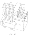
- FIG. 57 is a partial perspective view of the semiconductor die carrier in accordance with the present invention plugged within a pluggable socket.
- FIG. 58 is a partial perspective view of a semiconductor die carrier in accordance with the present invention plugged within another pluggable socket.
- FIG. 59 is a partial perspective view of a semiconductor die carrier in accordance with the present invention plugged into the pluggable socket illustrated in FIG. 58 .
- FIG. 60 is a partial perspective view of a semiconductor die carrier in accordance with the present invention having leads extending straight out of one or more sides of the carrier.
- FIG. 61 is a partial perspective view of a semiconductor die carrier in accordance with the present invention including leads having an alternate foot configuration.
- FIG. 62 is a top view of a single-tier embodiment of a semiconductor die carrier in accordance with the present invention.
- FIG. 63 is a partial perspective view of a semiconductor die carrier in accordance with the present invention wherein the leads of at least one row alternate with vias extending into a substrate such as a PCB.
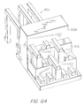
- FIG. 64 is a partial perspective view of a semiconductor die carrier in accordance with the present invention showing an arrangement of bonding extensions inside the carrier.
- FIG. 65 is a perspective view of a rounded lead configured in accordance with the present invention.
- FIG. 66 is a partial perspective view of a semiconductor die carrier in accordance with the present invention having round lead passages.
- FIG. 67 is a chart comparing various embodiments in accordance with the present invention with conventional QFP technology.
- a prefabricated semiconductor die carrier in accordance with the present invention has multiple rows of electrically conductive leads arranged at vertically spaced multiple levels around the periphery of the carrier. Such leads may also be arranged on the top or bottom of the carrier. Each of the leads is manufactured and assembled into the semiconductor die carrier prior to the die attach step as an individually manufactured lead, rather than as a sub-element of a lead frame, to facilitate the multiple-row, multiple-level structure.
- the leads of the semiconductor die carrier may be offset from other levels at the point where the leads extend through side walls of the carrier and/or staggered at the point where the leads connect to a PCB or other interface surface. At least the latter configuration allows traces on the PCB to be routed between the staggered leads.
- the leads of the semiconductor die carrier extend into the die carrier through the side walls of the die carrier, forming a series of vertically spaced rows of multiple leads around the semiconductor die.
- the portions of the leads extending through the side walls have wire bond terminals formed thereon.
- a wire bond insulator may be used to separate the rows of leads.
- the semiconductor die can be mounted within the carrier with the peripheral pads of the die facing up and away from the PCB, in a cavity-up configuration, or with the peripheral pads of the die facing down toward the PCB, in a flip-chip or cavity-down configuration.
- Encapsulation for the semiconductor die carrier of the present invention is performed by filling the die cavity with an epoxy, a liquid crystal polymer such as VECTRA (a trademark of Hoechst Celanese) or other high-temperature material.
- the semiconductor die carrier may be capped with a plastic component or thermally conductive cap that serves as a heat sink.
- the semiconductor die carrier of the present invention provides a package having a reduced size as compared to known semiconductor packages, yet increases the number of interconnects available for the designer and user.
- the die carrier may be pluggable or compatible with either the PTH or SMT methodology.
- the semiconductor die carrier is prefabricated and tested prior to introduction of the semiconductor die to the carrier, thereby increasing finished product yields and reducing total unit cost.
- the configuration of the die carrier allows the semiconductor die to be bonded from multiple rows of pads on the die to multiple levels of vertically spaced rows of leads while maintaining a very low profile for the die carrier.
- the semiconductor die carrier of the present invention provides better coplanarity of the feet of the leads when mounting using the SMT methodology, for example, thereby avoiding non-contact between the leads and the surface of the PCB. Such coplanarity is not always possible using conventional packaging technology due to the bending of the leads that is required when using a lead frame.
- FIG. 3 A perspective view of an embodiment of a prefabricated semiconductor die carrier in accordance with the present invention is shown in FIG. 3.
- FIG. 4 A partial view of the embodiment of FIG. 3 is shown in FIG. 4 .
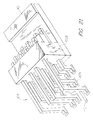
- the semiconductor die carrier includes a semiconductor die 101 ; an insulating substrate 102 , having a floor 102 a and a plurality of side walls 102 b; a plurality of leads 103 , including lower leads 103 a and upper leads 103 b; a plurality of bonding pads 104 formed on the semiconductor die; a plurality of bonding terminals 105 formed on the leads 103 , respectively; and a plurality of bonding wires 106 each connecting at least one of the bonding pads 104 of the die to a corresponding one of the bonding terminals 105 formed on the leads.
- both the semiconductor die and semiconductor die carrier of the embodiment of FIG. 3 are depicted as being square, both the semiconductor die and the die carrier could assume another shape, such as a rectangle having sides of different lengths.
- the number of sides the semiconductor die carrier can be varied, such that die carriers having twelve sides, for example, as depicted in FIG. 5, or eight sides, for example, as depicted in FIG. 6, are within the scope of the present invention.
- the die carriers of FIGS. 5 and 6 are designed to take up less space than four-sided die carriers and, as shown in FIG. 6, additional leads can be provided on the additional sides to achieve even greater efficiency. In accordance with the configuration of FIG. 6, for example, forty extra leads may be provided by positioning ten additional leads within each of the additional side walls.
- the semiconductor die carrier has been shown having two rows of leads 103 , only a single row of leads could be used, or more than two rows of leads would be used, as discussed in greater detail below.
- the semiconductor die 101 of the semiconductor die carrier can be a semiconductor die having a single row of bonding pads 104 arranged along each of its edges, as shown in FIG. 3, or a semiconductor die having, for example, two or more rows of bonding pads arranged along each of its edges.
- the bonding pads 104 could be arranged in straight rows and columns, or the bonding pads 104 could be arranged in some other configuration, for example, arranged such that the bonding pads from adjacent rows are staggered.
- the insulating substrate 102 of the semiconductor die carrier is made of a liquid crystal polymer or material having properties the same or similar to a liquid crystal polymer.
- the liquid crystal polymer for the insulating substrate 102 is VECTRA (trademark), which has a coefficient of thermal expansion that is approximately the same as or similar to the coefficient of thermal expansion for silicon.
- the insulating substrate 102 may be formed in a molding process carried out prior to inserting the leads 103 into the side walls 102 b of substrate, and prior to mounting the die 101 onto the floor 102 a of the substrate.
- a series of lead holes or passages 107 are molded within the side walls 102 b of the substrate, each of the passages for receiving a corresponding one of the leads 103 , and a series of ledges 108 are formed inside the side walls of the substrate around the periphery where the die is to be placed.
- the ledges 108 serve to support the leads 103 (during the wire bonding procedure, for example).
- the lead passages and/or ledges could be added after molding by, for example, removing material of the substrate to form the lead passages and/or by applying insulative material (using an adhesive or epoxy, for example) to form the ledges.
- FIG. 7 ( a ) is a view showing an example of the leads 103 inserted into the side walls 102 b prior to the fastening of the side walls to one another and to the floor 102 a.
- steps or notches may be molded on the bottom and/or corners of the side walls 102 b and on the sides of the floor 102 a to increase the glue area and surface area where the floor 102 a and side walls 102 b meet, thereby facilitating the formation of a stronger bond.
- the leads 103 are inserted into the side walls 102 b of the substrate 102 after formation of the lead passages 107 and ledges 108 .
- the leads 103 may be inserted individually one-by-one, or “gang-inserted” in groups. For example, in accordance with gang-inserting, all of the leads 103 for each side of the semiconductor die carrier could be inserted simultaneously, or all of the lower leads 102 a could be inserted simultaneously followed by a simultaneous insertion of the upper leads 103 b above such lower leads.
- the direction of lead insertion may be, for each side wall 102 b, from the outer surface of the side wall toward the inner surface of the side wall.
- Each of the leads 103 is inserted into a corresponding one of the lead passages 107 .
- the dimensions of the leads 103 and lead passages 107 are such that each lead 103 fits tightly within its corresponding lead passage 107 .
- each lead 103 can be further fastened within its corresponding lead passage 107 and/or onto a corresponding ledge 108 using an epoxy or other adhesive material.
- the leads may be formed within the side walls using an insert molding process.
- the leads 103 are supported by a bandolier or other fixture, and then the insulative substrate 102 or, alternatively, only the side walls 102 b of the insulative substrate, are molded around the leads.
- the resulting structure is extracted from the mold. If the resulting structure is a side wall with leads formed therein, that side wall is fastened together with other side walls and a floor to form the insulative substrate containing the leads. If the resulting molded structure is an insulative substrate already including a floor and a plurality of side walls, then no further fastening of the side walls to one another or to the floor is required.
- the lower leads 103 a and upper leads 103 b are similarly shaped, although the vertically-extending sections of the lower leads are shorter than the vertically-extending sections of the upper leads.
- the horizontally-extending sections of the lower leads 103 a could be longer, shorter, or the same length as the horizontally-extending sections of the upper leads 103 b.
- the lower leads 103 a and upper leads 103 b are aligned in a straight line with respect to one another rather than staggered.
- a corresponding lower lead 103 a is positioned directly beneath that upper lead.
- the lower leads 103 a and upper leads 103 b could be staggered with respect to one another.
- none of the lower leads 103 a would be beneath any of the upper leads 103 b. Instead, progressing along a given one of the side walls 102 b, every other lead would be a lower lead 103 a or an upper lead 103 b.
- each of the leads 103 includes a bonding extension section 1031 having a bonding terminal 105 formed on an end portion thereof; a stabilizing section 1032 ; and an external lead section 1033 .
- Each lead 103 may be formed of beryllium copper, phosphor bronze, brass, a copper alloy, tin, gold, palladium, or any other suitable metal or conductive material, and the bonding terminal 105 may be a gold-plated pad or pad formed of another suitable conductive material.
- the bonding extension section 1031 is a relatively long and narrow portion of the lead 103 which protrudes toward the interior of the semiconductor die carrier from the inner surface of a corresponding one of the side walls 102 b.
- the lower surface of the bonding extension section 1031 is supported by the floor 102 a of the substrate if the lead is a lower lead 103 a, or is supported by a corresponding one of the ledges 108 if the lead is an upper lead 103 b.
- the substrate 102 can be formed without ledges, in which case the upper leads would be suspended in air above the floor 102 a rather than being supported by a ledge.
- the bonding terminal 105 may be, for example, a bonding pad to which a bonding wire 106 for attachment to a corresponding bonding pad 104 on the die 101 can be connected.
- the stabilizing section 1032 of each lead 103 is the portion of the lead that is anchored within a side wall 102 b of the substrate 102 .
- the stabilizing section has a larger cross-sectional area than that of the bonding extension section 1031 and may also have a larger cross-sectional area than that of the external lead section 1033 .
- the thick stabilizing section retains the lead and prevents forces exerted on the external lead section from transferring to the bonds associated with bonding wire 106 .
- the stabilizing section 1032 may be taller than the bonding extension section 1031 and the external lead section 1033 .
- the stabilizing section 1032 could be wider than the bonding extension section 1031 and the external lead section 1033 , as in FIG.
- FIG. 8 ( b ) shows that the stabilizing section 1031 could be the same size in cross-section as the external lead section 1033 while, at the same time, having a height that is different than that of the bonding extension section 1031 .
- each 103 lead can be positioned so that the inwardly-facing surface of that part of the stabilizing section 1032 which is higher than the bonding extension section 1031 is level or flush with the inner surface of its corresponding side wall 102 b.
- the lead passage 107 for each lead 103 can be narrowed at the end of the passage located nearest the interior of the carrier (for example, only narrow enough to allow passage of the bonding extension section 1031 through the side wall 102 b of the substrate) so as to prevent the lead from being inserted too far into the side wall of the substrate.
- each lead 103 may be sloped at the juncture between the bonding extension section 1031 and the stabilizing section 1032 , to allow for ease of insertion into its corresponding lead passage 107 .
- the sloped surface may also serve to prevent over-insertion of the lead 103 if the corresponding lead passage 107 is modified to be narrowed or tapered at the end of the passage located nearest the interior of the carrier.
- the narrowing or tapering at the end of the lead passage 107 could occur at a slope corresponding to that of the sloped surface of the lead 103 to allow for a tight fit of the lead within its corresponding passage.
- each lead could be configured so that the bonding extension section 1031 extends from a middle section of the stabilizing section 1032 (like the external lead section 1033 shown in FIG. 8 ( a )) or from an upper section of the stabilizing section 1032 (such that the upper surfaces of the bonding extension section 1031 and stabilizing section 1032 would be level, for example).
- each lead 103 could be configured so that the external lead section 1033 extends from a lower section of the stabilizing section 1032 (like the bonding extension section 1031 shown in FIG. 8 ( a ), which has a lower surface that is level with respect to the lower surface of the stabilizing section 1032 ) or from an upper section of the stabilizing section 1032 (such that the upper surfaces of the external lead section 1033 and stabilizing section 1032 would be level, for example).
- the external lead section 1033 includes a horizontally-extending section 1033 a, a corner section 1033 b, a vertically-extending section 1033 c, and a foot section 1033 d.
- the configuration and length of the horizontally-extending and vertically-extending sections for each individual lead 103 are selected based on design requirements and, in particular, based on whether that lead will be used as a lower lead 103 a or an upper lead 103 b.
- the horizontally-extending sections 1033 a of the upper leads 103 b may be longer than the horizontally-extending sections of the lower leads 103 a
- the vertically-extending sections 1033 c of the upper leads may be longer than the vertically-extending sections of the lower leads.
- the horizontally-extending section 1033 a of the external lead section 1033 extends out of the stabilizer section 1032 in a direction away from the outer surface of the corresponding side wall 102 b.
- the external lead section 1033 bends downward at a corner section 1033 b between the horizontally-extending section 1033 a and the vertically-extending section 1033 c.
- the vertically-extending section 1033 c terminates in a foot section 1033 d.
- the PCB contact surface for the foot section 1033 d may have a larger cross-section than that of the vertically-extending section 1033 c, as shown in FIG. 8 ( a ), or, alternatively, may have a Butt Lead configuration, as shown in FIG. 12, such that the cross-section of the contact surface for the foot section is the same as that of the vertically-extending section.
- foot sections 1033 d shown in FIGS. 8 ( a ) and 12 are configured for mounting to a PCB or other interface surface in accordance with SMT methodology.
- foot section 1033 d could be configured for mounting in a PCB or the like in accordance with PTH technology, as shown in FIG. 13, for example.
- FIG. 14 which is another partial view of the semiconductor die carrier shown in FIG.
- FIG 3 depicts an example of the connection of a first die bonding pad 104 a to the bonding terminal 105 on a lower lead 103 a, and the connection of a second die bonding pad 104 b to the bonding terminal 105 on an upper lead 103 b. Each of these connections occurs via a bonding wire 106 . Such bonding wire connections may be performed for all of the bonding pads 104 formed on the die 101 .
- encapsulation may be carried out by filling the cavity defined by the floor 102 a and the side walls 102 b of the substrate 102 with epoxy, a liquid crystal polymer such as VECTRA (trademark), or other high-temperature material.
- the semiconductor die carrier might then be capped with a plastic component or thermally-conductive cap that may serve as a heat sink, and thereafter sealed.
- the encapsulation step is optional.
- the heat sink and high-temperature material which may be used for encapsulation facilitate the heat dissipation capabilities of the semiconductor die carrier.
- a two-row semiconductor die carrier in accordance with the present invention may have, for example, a height of 2.0 mm, a width of 17.9 mm, and a lead row length of 8.7 mm.
- the semiconductor die carrier of the present invention can be manufactured to be approximately 64% smaller than conventional 128-pin QFPs, and at the same time provides 16 extra leads.
- a lead 103 in accordance with the present invention may have a bonding extension section 1031 that is 1.5 mm in length; a stabilizing section 1032 that is 1.0 mm in length, and an external lead section 1033 having a vertically-extending section 1033 c that varies in length depending whether the lead is an upper lead or a lower lead.
- the lengths of the horizontally-extending sections and vertically-extending sections 1033 a and 1033 c of each lead, respectively, depend upon whether or not that lead is to be used as a lower lead 103 a or an upper lead 103 b.
- the lengths of the horizontally-extending sections 1033 a of the upper and lower leads, respectively, could be the same, with only the lengths of the vertically-extending sections 1033 c being different.
- the foot section 1033 d of a lead 103 configured for mounting in accordance with SMT can have a cross-section of 0.2 ⁇ 0.4 mm, for example, for mounting on a PCB bonding pad 109 having an exemplary cross-section of 0.4 ⁇ 0.6 mm.
- FIG. 14 illustrates that each ledge may have a height of 0.7 mm, for example.
- FIG. 15 A perspective view of another embodiment of a prefabricated semiconductor die carrier in accordance with the present invention is shown in FIG. 15 .
- the embodiment of FIG. 15 essentially corresponds to the embodiment shown in FIG. 3, except that three vertically spaced rows of multiple leads 103 a, 103 b, and 103 c are used instead of two of such rows.
- Such a configuration enhances the interconnect capabilities of the semiconductor die carrier.
- ledges 108 might be applicable to the three-row semiconductor die carrier in accordance with the present invention.
- the semiconductor die carrier of FIG. 15 may be manufactured in the same manner that the carrier shown in FIG. 3 is manufactured. More particularly, for the embodiment of FIG. 15, the leads 103 are formed within the side walls 102 b via insertion or an insert molding procedure; the semiconductor die 101 is adhered to the floor 102 a; the bonding pads 104 of the die are connected to the bonding terminals 105 of the leads 103 , respectively; and the cavity of the carrier could be filled with high-temperature material such as VECTRA (trademark) and/or a cap could be sealed on top of the carrier. Exemplary dimensions for the embodiment of FIG. 15 are a height of 2.7 mm; a width of 21.5 mm; and a lead row length of 11.8 mm. In this configuration, the semiconductor die carrier of FIG. 15 can be configured to provide 208 leads using approximately half of the area (for example, board area) of that required by conventional QFP technology.
- FIG. 16 is a partial perspective view of the embodiment shown in FIG. 15, illustrating details of the manner in which the leads 103 are arranged within the side walls 102 b of the substrate 102 .
- FIG. 17 is a partial side view of the semiconductor die carrier of FIG. 15 prior to insertion of the leads 103 into the lead passages 107
- FIG. 18 is a partial side view of the semiconductor die carrier of FIG. 15 after insertion of the leads 103 .
- the patterns separated by dotted lines in FIGS. 17 and 18 may repeat along the length of each side wall 102 b.
- FIG. 19 is a partial perspective view of the embodiment of FIG. 15 showing wire bonding details
- a three-row embodiment of the present invention can be used for packaging in connection with a semiconductor die having two or more rows of bonding pads 104 arranged along each of its edges.
- the semiconductor die could have a single row of bonding pads 104 aligned along each of its edges.
- ledges 108 are not shown in FIG. 15, such ledges are applicable to this embodiment.
- FIGS. 20 and 21 are partial perspective views of the embodiment of FIG. 15 illustrating details of the manner in which the leads 103 may interface with a PCB or other interface surface.
- FIG. 22 is a partial top view showing only the foot sections 1033 d of the leads 103 arranged on bonding pads 109 of a PCB or other interface surface. The configuration illustrated in FIG. 22 will be referred to herein as a footprint of the semiconductor die carrier.
- FIG. 23 is a partial top view showing the manner in which the leads 103 extend from the exterior surface of the side walls 102 b for mounting on a PCB or other interface surface. The patterns separated by dotted lines in FIGS. 22 and 23 may repeat along the length of each side wall 102 b.
- the arrangement of the leads 103 with respect to the PCB or other interface surface facilitates the routing of traces 110 on the interface surface upon which, if using SMT technology, for example, or within which, if using PTH technology, for example, the semiconductor die carrier is being mounted.
- the footprint of the semiconductor die carrier of FIG. 15 is arranged into three rows. The first row “a” of the footprint, closest to the side walls 102 b of the carrier, is defined by the foot sections of the lower leads 103 a.
- the second row “b” of the footprint, further from the side walls 102 b of the carrier, is defined by the foot sections of the middle leads 103 b; and the third row “c” of the footprint, furthest from the side walls 102 b of the carrier, is defined by the foot sections of the upper leads 103 c.
- the footprint for the three-row embodiment in accordance with the present invention may be configured such that, for each row of the footprint, the closest distance between adjacent foot sections is 0.3 mm, and the closest center-line to center-line distance between adjacent foot sections is 0.5 mm. This allows for the incorporation of high-density interconnect availability on the PCB or other interface surface upon or within which the leads 103 will be mounted.
- the aforementioned 0.3 and 0.5 mm distances may be applicable to the other embodiments (for example, one-row, two-row, and four-row embodiments) of the present invention.
- FIG. 24 A partial side view of the embodiment of FIG. 15 is shown in FIG. 24 .
- the illustration of FIG. 24 shows features of the semiconductor die carrier including a die bond adhesive 111 for mounting the die 101 on the floor 102 a; bonding wires 106 which, in each of the embodiments of the present invention, may be dimensioned to have a wire length of less than 1.0 to 2.5 mm, for example; a cavity filler 112 used to fill the cavity defined by the floor 102 a and side walls 102 b of the carrier during the encapsulation process; and a sealing cap 113 , made of plastic or other thermally-conductive material such as metal or VECTRA (trademark), and capable of functioning as a heat sink, for providing a cover for the semiconductor die carrier.
- a die bond adhesive 111 for mounting the die 101 on the floor 102 a
- bonding wires 106 which, in each of the embodiments of the present invention, may be dimensioned to have a wire length of less than 1.0 to 2.5 mm, for
- FIGS. 25-28 show various configurations relating to the placement of the semiconductor die 101 within the semiconductor die carrier. Although FIGS. 25-28 depict an embodiment having three-row configuration, it should be noted that the die placement configurations illustrated in these figures are also applicable to the other embodiments of the present invention, including the one-row and two-row embodiments discussed above and the four-row embodiments discussed below.
- FIG. 24 corresponds to a cavity-up configuration, in which the semiconductor die is mounted within the carrier with the peripheral pads of the die facing up and away from the PCB or other mounting surface
- FIG. 25 corresponds to a cavity-down or flip-chip configuration, in which the peripheral pads of the die face down toward the PCB or other interface surface.
- the die 101 is mounted on a heat sink cap 114 , preferably formed of a thermally conductive material, and then wire bonding, encapsulation, and sealing using a sealing cap 113 , preferably formed of VECTRA (trademark), take place.
- the heat sink cap 114 can be an integrally molded component of the substrate 102 , or attached to the substrate 102 after molding of the substrate is completed.
- FIG. 26 shows that the semiconductor die 101 may be embedded or placed into an indentation, similar to the size of the semiconductor die, formed in the floor 102 a for receipt of the die.
- the top surface of the die is located below the bonding extension sections 1031 of the lower leads 103 a.
- FIG. 27 shows the placement of the semiconductor die 101 on top of a flat floor 102 a.
- the top surface of the semiconductor die 101 is the same level or similar in height to the height of the bonding extension sections 1031 of the lower leads 103 a.
- FIG. 28 shows the placement of the semiconductor die 101 on a raised platform 115 , similar to the size of the die, formed in the interior of the semiconductor die carrier.
- the raised platform 115 may be an integrally molded component of the substrate 102 , or attached to the substrate 102 after molding of the substrate is completed.
- the semiconductor die 101 may be mounted using an adhesive material, epoxy, or the like.
- FIG. 29 ( a ) shows a semiconductor die carrier similar to the one shown in FIG. 29 ( a ), except that the ledges 108 in FIG. 29 ( b ) fill in the gaps between adjacent leads of the same row, and only three rows of leads are shown in FIG. 29 ( b ). In other words, in FIG. 29 ( b ), the ledges 108 are not undercut. This simplifies the carrier mold.
- FIG. 29 ( a ) essentially corresponds to the embodiments shown in FIGS. 3 and 15, for example, except that four vertically spaced rows of multiple leads 103 a, 103 b, 103 c, and 103 d are used instead of two or three of such rows. Such a configuration further enhances the interconnect capabilities of the semiconductor die carrier.
- FIG. 29 ( a ) illustrates that, in all the embodiments of the present invention, the stabilizing section 1032 of each lead 103 may overlap or extend beyond the inner surface of its corresponding side wall 102 b, if desired.
- a stop such as that depicted in FIG. 10 could be used to prevent over-insertion of the leads.
- the semiconductor die carrier of FIG. 29 ( a ) is manufactured in the same manner that the die carriers shown in FIGS. 3 and 15 are manufactured. More particularly, for the embodiment of FIG. 29 ( a ); the leads 103 are formed within the side walls 102 b via insertion or an insert molding procedure; the semiconductor die 101 is adhered to the floor 102 a; the bonding pads 104 of the die are connected to the bonding terminals 105 of the leads 103 , respectively; and the cavity of the carrier could be filled with high-temperature material such as VECTRA (trademark) and/or a cap could be sealed on top of the carrier. Exemplary dimensions for the embodiment of FIG.
- VECTRA trademark
- the semiconductor die carrier of FIG. 29 ( a ) can be manufactured to be approximately 57% smaller than conventional 304-pin QFPs.
- FIG. 30 is a side view of the semiconductor die carrier of FIG. 29 ( a ) prior to insertion of the leads 103 into the lead passages 107
- FIG. 31 is a side view of the semiconductor die carrier of FIG. 29 ( a ) after insertion of the leads 103 .
- the patterns separated by dotted lines in FIGS. 30 and 31 may repeat along the length of each side wall 102 b.
- the arrangement of the leads 103 within the side walls 102 b allows the bonding extension sections of the leads to be positioned to facilitate the connecting of the bonding terminals 105 of the leads to the bonding pads 104 on the semiconductor die 101 .
- a four-row embodiment in accordance with the present invention can be used for packaging in connection with a semiconductor die 101 having two or more rows of bonding pads 104 arranged along each of its edges.
- the semiconductor die 101 could have a single row of bonding pads 104 aligned along each of its edges.
- FIG. 32 is a partial perspective view of the embodiment of FIG. 29 ( a ) illustrating details of the manner in which the leads may interface with a PCB or other interface surface.
- FIG. 33 ( a ) is a partial perspective view of a multiple-wall configuration in accordance with the embodiment of the semiconductor die carrier illustrated in FIG. 29 ( a ).
- each of the side walls 102 b comprises an inner wall 102 b 1 and an outer wall 102 b 2 , with a cavity separating the inner and outer walls.
- each side wall 102 b in the multiple-wall configuration may comprise an inner wall, an outer wall, and one or more walls between the inner and outer walls.
- the multiple-wall configuration eases insertion of the leads 103 into the side wall. After lead insertion, the cavity or cavities between the inner and outer walls may be filled with an epoxy or other adhesive, thereby retaining and stabilizing the leads, sealing the carrier, and preventing contamination.
- the inner lead passage 107 1 and outer lead passage 107 2 could have the same cross-sectional dimensions.
- the inner and outer lead passages 107 1 and 107 2 could have different cross-sectional dimensions.
- FIG. 33 ( b ) is a perspective view of a lead 103 configured for use with a multiple-wall configuration such as that shown in FIG. 33 ( a ).
- the stabilizing section 1032 of each lead may include an unnotched portion 1032 a, a notched portion 1032 b, and an unnotched portion 1032 c.
- the unnotched portions 1032 a and 1032 c may be disposed within the inner and outer walls of the multiple-wall configuration, respectively, and the notched portion may be positioned in a cavity between such walls.
- the notch in the stabilizing section provides additional surface area for contact with the epoxy or other adhesive filling the cavity between the inner and outer walls.
- FIG. 33 ( c ) is a perspective view of another lead 103 configured for use with a multiple-wall configuration such as that shown in FIG. 33 ( a ).
- the stabilizing section 1032 may include a raised portion 1032 d which provides additional surface area for contact with the epoxy or other adhesive filing the cavity between the inner and outer walls and, at the same time, which can act as a stop against an inner wall to prevent, for example, the over-insertion of the lead 103 .
- FIG. 33 ( d ) is a partial perspective view illustrating the raised portion 1032 d functioning as a stop when used in connection with an outer wall 102 b 2 allowing the raised portion to pass therethrough and an inner wall 102 b 1 which does not allow the raised portion to pass therethrough.
- FIG. 34 is a partial top view of an exemplary footprint which is suitable for use with the embodiment of FIG. 29 ( a ).
- FIG. 35 is a partial top view showing the manner in which the leads 103 extend from the exterior surface of the side walls 102 b for mounting on bonding pads 109 of a PCB or other interface surface.
- the patterns separated by dotted lines in FIGS. 34 and 35 may repeat along the length of each side wall 102 b.
- the arrangement of the leads 103 with respect to the PCB or other interface surface facilitates the routing of traces on the PCB or other interface surface upon which, if using SMT technology, for example, or within which, if using PTH technology, for example, the semiconductor die carrier is being mounted.
- the footprint of the semiconductor die carrier of FIG. 29 ( a ) is arranged into four rows.
- the first row “a” of the footprint, closest to the side walls 102 b of the carrier, is defined by the foot sections of the lower leads 103 a;
- the second row “b” of the footprint, further from the side walls 102 b of the carrier, is defined by the foot sections of the lower middle leads 103 b;
- the third row “c” of the footprint, still further from the side walls 102 b of the carrier, is defined by the foot sections of the upper middle leads 103 c;
- the fourth row “d” of the footprint, furthest from the side walls 102 b, is defined by the foot sections of the upper leads 103 d.
- FIG. 36 is a partial view of the embodiment of the semiconductor die carrier of FIG. 29 ( a ) including additional components designated by reference numerals 116 and 117 .
- reference numeral 116 designates an insulating separator formed of insulative material such as a thin sheet of polyester film or MYLAR (a trademark of E. I. DuPont de Nemours and Company), and reference numeral 117 designates a support column formed of, for example, a liquid crystal polymer such as VECTRA (trademark).
- the insulating separator 116 and/or the support column 117 can be integrally molded components of the substrate 102 or, alternatively, can be attached to the substrate 102 after molding of the substrate is completed. It should be noted that while FIG. 36 only shows one or two leads from each of the four vertically spaced rows, in the configuration of FIG.
- the leads 103 extend along essentially the entire length of each of the side walls 102 b of the semiconductor die carrier as in previously discussed embodiments.
- the insulating separator 116 also extends along essentially the entire length of each side wall 102 b. Also, while not shown in FIG. 36, several support columns 117 may be regularly or irregularly spaced along each of the side walls 102 b of the semiconductor die carrier to provide balanced support of the insulating separator 116 along its length.
- the support columns 117 arranged at regular or irregular intervals along each side wall 102 b of the semiconductor die carrier provide support for the insulating separator 116 for that side wall.
- the insulating separator 116 provides support for the bonding wires 106 , and prevents shorting of the bonding wires by providing insulation between the multiple rows of leads.
- Such a configuration facilitates the attachment of bonding wires between corresponding pairs of the bonding pads 104 on the die 101 and the bonding terminals 105 and, additionally, facilitates the use of increased numbers of bonding pads 104 per linear inch on the semiconductor die.
- the insulating separator 116 makes it easier to more reliably connect bonding wires to a semiconductor die having two or more rows of bonding pads arranged along each of its edges.
- the configuration of FIG. 36 could also be used with a semiconductor die 101 having, for example, a single row of bonding pads 104 arranged along each of its edges.
- FIG. 37 illustrates features of the semiconductor die carrier of the present invention including a die bond adhesive 111 for mounting the die 101 on the floor 102 a; a cavity filler 112 used to fill the cavity defined by the floor 102 a and side walls 102 b of the carrier during the encapsulation process; and a sealing cap 113 made of plastic or other thermally-conductive material such as metal or VECTRA (trademark), and capable of functioning as a heat sink, for providing a cover for the semiconductor die carrier.
- a die bond adhesive 111 for mounting the die 101 on the floor 102 a
- a cavity filler 112 used to fill the cavity defined by the floor 102 a and side walls 102 b of the carrier during the encapsulation process
- a sealing cap 113 made of plastic or other thermally-conductive material such as metal or VECTRA (trademark), and capable of functioning as a heat sink, for providing a cover for the semiconductor die carrier.
- prefabricated semiconductor die carrier having one row of multiple leads or two, three, or four vertically spaced rows of multiple leads. While not shown in the accompanying drawings, in accordance with the present invention, prefabricated semiconductor die carriers having five or more vertically spaced rows of multiple leads are also contemplated. Such prefabricated semiconductor die carriers are considered to be within the spirit and scope of the present invention.
- FIG. 38 is a partial side view illustrating an aspect of the present invention that is applicable to all of the previously-discussed embodiments.
- FIG. 38 shows that a multi-layer ceramic component 118 with steps formed along its sides, one step for each row of the leads 103 , may be used to achieve electrical interconnection between the leads and the bonding wires 106 .
- the multi-layer ceramic component 118 has a plurality of levels of electrically conductive material and pads along the steps therein to allow for the transmission of signals between the leads 103 and the bonding wires 106 connected to the die 101 . Connection between the leads 103 and the ceramic component 118 may be achieved by soldering, for example.
- the configuration of FIG. 38 has been found to be particularly useful with smaller dies having larger I/O requirements.
- ceramic components are also applicable to multi-die modules, discussed below, and to configurations incorporating bonding technologies such as C4 and TAB, for example.
- bonding technologies such as C4 and TAB, for example.
- a stepped ceramic component such as that depicted in FIG. 18 facilities the incorporation of C4 and TAB bonds within the various embodiments of the present invention.
- FIG. 39 ( a ) is a partial side view illustrating another aspect of the present invention that is applicable to all of the previously-discussed embodiments.
- the foot portion 1033 d for each of leads 103 a, 103 b, and 103 c is SMT-compatible. However, such foot portions are not coplanar.
- the foot portion of the middle lead 103 b is lower than the foot portion of the lower lead 103 a
- the foot portion of the upper lead 103 c is lower than the foot portion of the middle lead 103 b.
- Such non-coplanarity renders the semiconductor die carrier of the present invention suitable for use with a multi-layer substrate or PCB 119 having SMT-compatible surfaces or bonding pads 109 a, 109 b, and 109 c formed at various layers thereof (for example, formed on an upper layer 119 a, a middle layer 119 b, and a lower layer 119 c thereof).
- Crane et al. entitled “APPARATUS HAVING INNER LAYERS SUPPORTING SURFACE-MOUNT COMPONENTS,” filed on even date herewith, and expressly incorporated herein by reference, discloses multi-layer substrate and PCBs suitable for use in connection with the present invention and, in particular, the configuration of the present invention illustrated in FIG. 39 ( a ).
- Such substrates are equipped with plated or unplated wells 120 b and 120 c each providing a passage to the inner layer bonding pads.
- the wells may be filled with solder 121 b and 121 c to maintain electrical contact between corresponding pairs of bonding pads and leads and to provide mechanical stability.
- FIG. 39 ( b ) depicts structure similar to that shown in FIG. 39 ( a ), except in FIG. 39 ( b ) the lead 103 c is SMT-mounted to an outer layer of the multi-layer substrate rather than to an inner layer.
- the leads from different rows are aligned in a straight line with respect to one another rather than being staggered, such that the lead configuration along the sides of the carrier and on the multi-layer substrate does not require any gaps for routing traces. This allows for a three-row lead configuration that is very high in density.
- FIG. 40 is a partial perspective view illustrating yet another aspect of the present invention that is applicable to all of the previously-discussed embodiments.
- each of the lead passages 107 in one or more (e.g., all) of the side walls 102 b may be molded to have a primarily rectangular configuration with rounded corners (i.e., a “dog bone” configuration).
- the rounded corners serve to relieve some of the stresses which can result on the plastic of the side walls when the leads 103 (not shown in FIG. 40) are inserted.
- FIG. 41 is a perspective view of another aspect of the present invention that is applicable to all of the previously-discussed embodiments.
- a plurality (e.g., four) of semiconductor dies 101 may be incorporated within a prefabricated semiconductor die carrier in accordance with the present invention, thus allowing an even more efficient usage of materials and board space.
- a multi-layer ceramic component 122 having a plurality of levels of electrically conductive material therein, is glued or otherwise adhered to the floor 102 a, and the plurality of semiconductor dies 101 are glued or otherwise adhered to the multi-layer ceramic component.
- the dies may or may not be electrically connected to the multi-layer ceramic component using C4, wire bond, TAB, or other bonding technologies.
- C4, TAB, or like bonding conductive lands on the bottom surface of the dies are used to provide electrical interconnection between the dies and the ceramic component 122 .
- wire bonding bonding wires (not shown) connected at one end to the bonding pads 104 and at the other end to the ceramic component 122 are used to provide electrical interconnection between the dies and the ceramic component.
- the leads 103 are either soldered to the ceramic component 122 , or electrically connected to the ceramic component using bonding wires (not shown).
- bonding wires (not shown)
- For the bonding pads 104 along the outwardly-facing edges of each semiconductor die 101 rather than transmitting the signals between the leads 103 and the bonding pads 104 via the multi-layer ceramic component 122 , such signals may be transmitted directly between the bonding pads and leads via bonding wires (not shown) directly connected to the leads 103 at one end and directly connected to the bonding pads 104 at the other end.
- FIG. 41 shows the incorporation of four semiconductor dies within a single prefabricated semiconductor die carrier in accordance with the present invention, either more or less dies per semiconductor die carrier are contemplated. As stated previously, the incorporation of a plurality of semiconductor dies within a single die carrier allows more effective usage of materials and board space.
- FIG. 42 is a partial perspective view of yet another aspect of the present invention that is applicable to all of the previously-discussed embodiments. As seen from FIG. 42, some of the leads 103 may be oriented in an upward direction, while others of the leads may be oriented in a downward direction. The number of rows of upwardly-oriented and downwardly-oriented leads may be the same, as depicted in FIG. 42, or the number of upwardly-oriented leads may be greater than or less than the number of downwardly-oriented leads.
- the configuration of FIG. 42 allows the mounting of the leads to one or more substrates located above the semiconductor die carrier and also to one or more PCBs located below the semiconductor die carrier and, therefore, is particularly useful for the purpose of creating stacks of PCBs or other substrates.
- FIG. 43 is a partial perspective view of still another aspect of the present invention that is applicable to all of the previously-discussed embodiments.
- the prefabricated semiconductor carrier in addition to having leads 103 extending sideways in a horizontal direction from its side walls 102 b, the prefabricated semiconductor carrier may also have leads 123 extending downward in a vertical direction from its floor 102 a. This configuration allows for more leads on a single semiconductor die carrier and provides increased design flexibility and versatility.
- the top portions of the leads 123 may have plated (gold-plated, for example) tips 124 to facilitate bonding with the bonding wires 106 .
- the downwardly-extending leads 123 may be positioned around the periphery of the semiconductor die area. Additionally, or alternatively, the downwardly-extending leads 123 may extend from the portions of the floor 102 a directly beneath the semiconductor die area. This could be accomplished, for example, by interposing a multi-layer ceramic component (not shown) between each semiconductor die 101 and the floor 102 a. Each semiconductor die 101 could be electrically connected to the interposed multi-layer ceramic component by wire bonding, tape automated bonding (TAB), or controlled collapse die connection (C4) interconnects, or the like, and the interposed multi-layer ceramic component could be electrically connected to the leads 123 using ball grid array (BGA) technology.
- BGA ball grid array
- each semiconductor die 101 could be directly electrically connected to the tip portions 124 of the downwardly-extending leads 123 using C4 interconnect technology, for example.
- FIG. 44 is a partial bottom view showing a nested arrangement for the downwardly-extending leads 123 , with the leads being arranged into a plurality of groups 125 .
- the groups 125 are arranged in rows and columns on the floor 102 a (the dotted lines in FIG. 44 designate a row and a column, respectively); the electrical interconnect components of adjacent rows of the arrangement are staggered as are the groups from adjacent columns of the arrangement; and the groups are interleaved among one another in a nested configuration such that a portion of each group of contacts overlaps into an adjacent row of the groups of contacts or an adjacent column of the groups of contacts.
- the nested configuration in FIG. 44 can be modified to provide even greater densities.
- An example of one contemplated modification is depicted in FIG. 45 .
- the groups of contacts 125 are arranged in rows and columns on the floor surface 102 a; and at least lead 123 of each group 125 includes a front surface 126 facing outwardly and away from that group along a line initially intersected by a side surface 127 of a lead from another group of contacts.
- adjacent groups of contacts are offset such that a line drawn from the center of a group through the center of a contact for that group does not intersect the center of any of the groups directly adjacent that group.
- the distance d between like surfaces of the leads 123 may be 1.5 mm; and the overall density for the arrangement may be 1,156 contacts per square inch.
- FIGS. 44 and 45 may be modified to include a space 128 at a center portion thereof to allow the use of wire bonding, TAB, and the like.
- FIGS. 46 and 47 ( a ), respectively, are examples of the manner in which the arrangements of FIGS. 44 and 45 can be modified to include a space 128 .
- FIGS. 44 - 47 ( a ) use cross-shaped groups of contacts 125 , other shapes are contemplated.
- An array of groups of contacts 125 each having an H-shaped space between its contacts may be used, for example, as seen from FIG. 47 ( b ).
- the array of FIG. 47 ( b ) may provide a density of 636 contacts per square inch, for example.
- FIG. 48 includes two flowcharts.
- the flowchart at the left illustrates steps performed in the manufacturing of a conventional molded plastic semiconductor package.
- the flowchart at the right illustrates steps performed in a manufacturing process for producing a prefabricated semiconductor carrier in accordance with the present invention.
- the present invention entails fewer steps following the die bond procedure as compared to conventional manufacturing processes.
- the substrate 102 including the floor 102 a and side walls 102 b and, if desired, lead passages 107 and ledges 108 , are integrally formed using a molding process.
- the lead passages and/or ledges could be added after molding by, for example, removing material of the substrate to form the passages and/or by applying insulative material (using an adhesive or epoxy, for example) to form the ledges.
- Components such as raised platform 115 , insulating separator 116 , and/or support columns 117 could also be formed either integrally during the molding process, or such elements could be added after molding.
- the floor 102 a and side walls 102 b could be molded separately, and then fastened together using an epoxy or other adhesive.
- VECTRA trademark
- the substrate could be formed around the leads in an insert molding process.
- a step S 2 the leads 103 are formed.
- the lead formation step S 2 entails punching or stamping out individual leads from strips or drawn wire using, for example, a die. Applicants have found that by individually manufacturing each lead 103 , rather than using a lead frame to manufacture such leads, manufacturing costs are reduced and, at the same time, yield is increased.
- the aforementioned lead-manufacturing methods allow for selective plating and automated insertion.
- the leads for stamping can either be loose, on a bandolier carrier 129 (see, for example, FIG. 49 ), or on a strip since the asymmetrical shape lends itself to consistent orientation in automated assembly equipment.
- the different length external lead sections assist with orientation and vibratory bowl feeding during automated assembly.
- the present invention is compatible with both stitching and gang-insertion assembly equipment.
- the insulative components have been designed to facilitate automatic and robotic insertion onto PCBs or in termination of wire to connector.
- FIGS. 49 ( a ) and 49 ( b ), collectively referred to herein as “FIG. 49 ,” show the placement of the leads 103 on a bandolier or other fixture 129 during formation of the semiconductor die carrier.
- the leads may be stamped in an L-shaped version as depicted, or stamped in a straight version and then bent to achieve the L-shaped configuration.
- the use of a bandolier, in accordance with the present invention is applicable to the formation of both straight and L-shaped versions of the leads 103 .
- Step S 3 of FIG. 48 involves inserting the leads 103 into the side walls 102 b of the substrate 102 .
- the leads may be inserted into the side walls before they are fastened to one another or to the floor.
- Each of the leads 103 is inserted into a corresponding one of the lead passages 107 in the side walls 102 b.
- the dimensions of the leads 103 and lead passages 107 are such that each lead fits tightly within it corresponding lead passage 107 .
- each lead 103 can be further fastened within its corresponding lead passage 107 and/or onto a corresponding ledge 108 using an epoxy or other adhesive material.
- step S 4 mechanical testing is performed to ensure that the leads 103 are securely fastened within the substrate 102 ; to ensure that coplanarity of the leads 103 falls within an acceptable range; to ensure that each lead is aligned properly within its respective lead passage; and the like. Also, electrical testing is performed to ensure that signals can be transmitted properly through the leads of the carrier to the exterior of the carrier, and vice versa; and to ensure that none of the leads are shorted or would be likely to short during subsequent stages of the manufacture and usage of the semiconductor die carrier.
- step S 5 the substrate 102 having leads 103 disposed therein is packaged and then shipped to the place where a semiconductor die, manufactured in step S 6 , will be bonded to the substrate.
- transportation packaging such as that illustrated in FIGS. 50-55 is used to accomplish shipping.
- the packaging illustrated in FIGS. 50-55 can be used to transport the semiconductor die carrier to the location at which die bonding will occur, and from that location to the customer following the die bonding.
- FIG. 50 A first type of transportation packaging is shown in FIG. 50 .
- the type of packaging shown in FIG. 50 will be referred to herein as a carrier tray.
- the carrier tray includes an upper section 130 and a lower section 131 .
- Each of these sections comprises a base 132 upon which are formed one or more (e.g., twenty) support platforms 133 each having a set of corresponding support segments 134 associated therewith.
- FIGS. 51-53 are views showing a semiconductor die carrier positioned within a carrier tray such as that depicted in FIG. 50 .
- the semiconductor die carrier of FIGS. 51 and 52 has leads 103 which point downward, while the leads from the semiconductor die carrier in FIG. 53 point upward.
- the support platform 133 performs the function of ensuring that the leads 103 of the semiconductor die carrier do not touch the base 132 . Such prevention reduces the occurrences of breakage and other potential complications.
- the support segments of the upper section 130 are positioned slightly closer to one another than are the support segments of the lower section 131 , or vice-versa, so that the upper and lower sections may be mated or plugged together prior to shipping for protection of the semiconductor die carrier.
- the lower section 131 of the die carrier tray may hold the semiconductor die carrier with a main surface of the die carrier facing upward, so that when the upper section 130 is removed at a destination location, such as the die assembly location, the die carrier can be removed (via suction, for example) to allow die assembly, automatic mating or plugging, and the like.
- the carrier tray is stable to an extent that die assembly or other processes could be performed on the semiconductor die carrier while it is residing in the carrier tray. This would eliminate the steps of removing and returning the semiconductor die carrier to the carrier tray during the manufacturing process.
- FIG. 54 ( a ) A second type of transportation packaging is shown in FIG. 54 ( a ).
- the type of packaging shown in FIG. 54 ( a ) is a plastic tube or sleeve 135 a having an open end and a closed end.
- a plurality of semiconductor die carriers are inserted through the open end in the plastic tube 135 a in sequential fashion.
- the first semiconductor die carrier to be inserted rests against the closed end of the plastic tube 135 a or a stop located adjacent the closed end, the second semiconductor die carrier to be inserted rests against the first, and so on.
- Each semiconductor die carrier may have a bar separator 135 b molded or otherwise formed thereon.
- the bar separator keeps the leads from adjacent semiconductor die carriers from tangling or contacting each other when the carriers are packaged in the tube.
- the die carriers are removed from the plastic tube in an order that is reversed with respect to the order of insertion into the plastic tube.
- FIG. 54 ( b ) shows a completed semiconductor die carrier having four bar separators 135 b formed thereon.
- each carrier may be provided with two bar separators (for example, two bar separators located on the same side wall of the carrier or two bar separators located on opposing side walls of the die carrier at opposing corners, such as the uppermost and lowermost bar separators illustrated in FIG. 54 ( b )) or some other number of bar separators.
- FIG. 55 A third type of transportation packaging is shown in FIG. 55 .
- the type of packaging shown in FIG. 55 will be referred to herein as tape-and-reel packaging for a pick-and-place machine.
- a conductive plastic tape 136 has a plurality of sprockets 137 and a plurality of cavities 138 formed therein. Each cavity may include a support platform 139 to isolate the leads of each semiconductor die carrier from the bottom of the cavity.
- a semiconductor die carrier is placed in each cavity 138 and then a tape structure (e.g., masking or cellophane tape) is adhered to the conductive tape 136 to hold the semiconductor die carriers within the cavities during shipping.
- a tape structure e.g., masking or cellophane tape
- the conductive tape 126 is then wound around a reel or other magazine for holding tape and then transported.
- a pick-and-place machine automatically feeds the reel using sprockets 137 , peels off the tape structure, and removes the die carriers for die assembly, mounting, or the like, using a suction procedure.
- the third type of packaging is reusable so that the same package can be used to transport the semiconductor die carrier to the location at which die bonding will occur, and from that location to the customer following die bonding.
- Step S 7 of FIG. 48 involves attaching the semiconductor die 101 to floor 102 a or another support surface (for example, a raised platform 115 ) within the semiconductor die carrier.
- the attachment may be carried out using an adhesive, an epoxy or the like.
- Step S 8 entails a bonding procedure wherein a bonding wire 106 is connected between components of a pair including a bonding pad 104 on the die 101 and a bonding terminal 105 on one of the leads 103 .
- the bonding wires allow electrical connection between the die 101 and the various leads 103 .
- step S 9 further electrical tests may be performed to provide additional assurance that an acceptable product is being manufactured.
- step S 10 encapsulation is performed by filling the cavity defined by the floor 102 a and the side walls 102 b of the substrate 102 with epoxy, a liquid crystal polymer such as VECTRA (trademark), or other high-temperature material. Then the semiconductor die carrier may capped with a plastic component or thermally-conductive cap that may serve as a heat sink, and thereafter sealed, although use of a cap is optional. It should be noted that when a cap is used, the aforementioned encapsulation step becomes optional. The heat sink and/or high-temperature material which may be used for encapsulation and sealing facilitate the heat dissipation capabilities of the semiconductor die carrier.
- step S 11 further mechanical and electrical quality control testing may be performed to increase the likelihood that the semiconductor die carrier will function as expected.
- the completed semiconductor die carrier is packaged and shipped to the customer.
- the semiconductor die carrier is packaged and shipped to the customer using the same transportation package it was received in.
- the transportation packaging illustrated in FIGS. 50-55 is particularly well-suited for performing this type of double-transport function.
- Step S 13 relates to the mounting of the finished semiconductor die carrier on or within an interface surface such as a PCB surface.
- an interface surface such as a PCB surface.
- either PTH technology or SMT methodology may be used to accomplish PCB interfacing or, alternatively, the carrier may be plugged into a pluggable socket mounted on a PCB or other interface device.
- FIG. 56 shows a lead 103 particularly well-suited for plugging into a pluggable socket.
- an external lead section 1033 having an expanded width additional mechanical strength is provided. Such mechanical strength facilitates plugging of the semiconductor die carrier into a pluggable socket.
- FIG. 57 shows a semiconductor die carrier in accordance with the present invention plugged into a pluggable socket.
- a pluggable socket in accordance with the present invention includes an insulative substrate 140 and a plurality of electrically conductive beams 141 .
- Each of the conductive beams 141 contacts a corresponding lead 103 from the semiconductor die carrier at one end, and at the other end, is attached to a PCB or other interface surface.
- the beams 141 may be attached to the interface surface by using the SMT method, as shown in FIG. 57, or by using PTH technology.
- the footprint pattern of the conductive beams 141 on the interface surface may be identical to any of the lead footprints discussed above and, as shown in FIG. 57, for example, preferably matches the footprint corresponding to the leads of the semiconductor die carrier with which the socket is mating. Such matching between the footprint of the leads 103 and the footprint of the beams 141 simplifies routing and trace design by allowing the same conductive PCB pattern to accommodate both pluggable and SMT-compatible die carriers.
- the portions of the beams 141 extending above the substrate 140 each apply a force to a corresponding one of the leads 103 in a direction away from the interior of the semiconductor die carrier (i.e., to the left in the illustration of FIG. 57 ). This force is sufficient to hold the semiconductor die carrier in close proximity to the socket and, at the same time, allows selectable plugging and unplugging of the semiconductor die carrier.
- the portions of the beams 141 extending above the substrate 140 are flexible and springy such that, prior to mating with leads from a semiconductor die carrier, the leads bend in the direction away from the interior of the semiconductor die carrier (to the left in the illustration of FIG. 57 ), and after mating, are upright as depicted in FIG. 57 .
- FIGS. 58 and 59 are similar to FIG. 57 in that they represent partial perspective views of a semiconductor die carrier in accordance with the present invention mounted within a socket that is attached to a PCB or other interface device using the SMT methodology.
- the force applied by the beams 141 against the leads 103 in FIGS. 58 and 59 is in a direction that is perpendicular with respect to the lengths of the leads.
- This force like the force associated with the socket of FIG. 57, is sufficient to hold the semiconductor die carrier in close proximity to the socket and, at the same time, allows plugging and unplugging of the semiconductor die carrier.
- the portions of the beams 141 extending above the substrate 140 are flexible and springy such that, prior to mating with leads from a semiconductor die carrier, the leads bend in a direction perpendicular with respect to the lengths of the leads, and after mating, are upright as depicted in FIGS. 58 and 59.
- the configurations of the footprints of the semiconductor die carrier facilitate the routing of traces on the PCB or other interface surface onto or within which the semiconductor die carrier is being mounted. Further mechanical and electrical testing can be performed after the mounting process is completed.
- the semiconductor die carrier of the present invention begins as a pre-formed platform into which the die is inserted. Encapsulation is then accomplished by capping and sealing the platform after it has been tested. This results in the elimination of the entire molding, bending, and clean-up processes and the related bonding of the carrier. Because the leads of the present invention are pre-formed and inserted into the plastic platform, they are undisturbed by additional procedures conventionally performed after the die is introduced into the semiconductor package. In the conventional process, the most sensitive aspects of the manufacturing process, encapsulating the die and electroplating and forming the leads, are performed after the die and the semiconductor package have been mated.
- the semiconductor die carrier of the present invention could be delivered to the die attach area completely tested for plating, mechanical integrity, and dimensional characteristics, and the die need only be inserted into packages meeting acceptable quality standards. The elimination of the intermediate processes also reduces labor costs.
- the semiconductor die carrier of the present invention can be configured with a precise number of leads easier than current designs due to the programmable nature of its assembly.
- a designer can specify varied numbers of leads or changes in package size, without the need to design and manufacture new lead frame configurations.
- both the number of leads on a side of a package, and the number of rows of leads can be varied simply by producing a new mold for the prefabricated platform and reprogramming the lead insertion equipment to vary the number of leads or lead configuration.
- FIGS. 60-65 illustrate additional aspects relating to the semiconductor die carrier of the present invention.
- FIG. 60 shows that the leads 103 may extend straight out from one or more of the side walls of the semiconductor die carrier without bending or turning in a vertical or downward direction. Such straight leads are compatible for plugging within a socket or, alternatively, can function as Butt Joint Leads for SMT-mounting to a substrate such as a PCB.
- a substrate such as a PCB.
- the PCB or other such substrate to which the leads of semiconductor die carrier are SMT-mounted would be perpendicular with respect to the floor of the carrier.
- FIG. 61 is a partial perspective view of a semiconductor die carrier in accordance with the present invention having an alternate foot configuration.
- the feet of the leads 103 are oriented such that the feet in the lower row 103 a point toward the semiconductor die carrier and the feet in the upper row 103 b point away from the carrier.
- This type of configuration reduces the total surface area taken up on the substrate (for example, a PCB) to which the semiconductor die carrier is mounted.
- the concept of foot portions alternately facing toward and away from the semiconductor die carrier is applicable to all of the embodiments of the present invention utilizing two or more rows of leads.
- FIG. 62 is a top view of a single-tier embodiment of a semiconductor die carrier in accordance with the present invention. As with the multi-tier embodiments of the present invention, the single-tier embodiment of FIG. 62 is formed using individually manufactured leads instead of leads from a lead frame.
- FIG. 63 is a partial perspective view of a semiconductor die carrier in accordance withe the present invention with the leads of at least one row (e.g., leads 103 b of the middle row) alternating with vias 142 extending into the substrate to which the semiconductor die carrier is mounted.
- every lead 103 b in the middle row of the configuration has a via located on either side of it.
- Each via may be routed to one or more of the adjacent leads from its row and/or from other ones of the rows of leads.
- the leads (and also the vias) in FIG. 63 are aligned in a straight line with respect to one another.
- the arrangement of FIG. 63 increases the number of leads that can be located along the side of the semiconductor die carrier.
- FIG. 64 is a partial perspective view of a semiconductor die carrier in accordance with the present invention showing an arrangement of bonding extensions within the carrier.
- the bonding extensions of one or more of the leads from an upper or middle row may extend into the semiconductor die carrier to the same extent as bonding extension sections from lower ones of the rows of leads.
- the bonding extensions adjacent to one another but on different rows have the same length, bringing their respective bonding areas to the same plane. This arrangement facilitates wire bonding by reducing the length of the wire bond for second and higher tiers of leads.
- FIG. 65 illustrates that the leads 103 for use in connection with the semiconductor die carrier of the present invention may have a rounded cross-section.
- the rounded lead 103 of FIG. 65 may include a flattened portion 105 which may be plated with gold or other conductive material and which may function as a bonding pad to allow attachment of the lead to a bonding wire.
- the other end of the rounded lead 103 has a nailhead-type Butt Joint configuration resulting in a foot 1033 d which takes up less area.
- FIG. 66 illustrates that the lead passages 107 in accordance with the present invention may be round.
- the round lead passages of FIG. 66 are not only applicable for use with round leads, but also are applicable for receiving square, rectangular, or other shapes of leads to establish a pressure fit relationship between the leads and lead passages.
- FIG. 67 is a chart showing the surface area taken up by embodiments of the present invention versus current QFP technologies.
- the advantages provided by the present invention over conventional packaging technology illustrate that the present invention, unlike conventional packaging technology, is capable of keeping pace with the rapid advances that are currently taking place in the semiconductor and computer technologies.
Abstract
Description
Claims (150)
Priority Applications (15)
| Application Number | Priority Date | Filing Date | Title |
|---|---|---|---|
| US08/208,586 US6339191B1 (en) | 1994-03-11 | 1994-03-11 | Prefabricated semiconductor chip carrier |
| TW083102269A TW242697B (en) | 1994-03-11 | 1994-03-16 | Prefabricated semiconductor chip carrier |
| DE69535712T DE69535712T2 (en) | 1994-03-11 | 1995-03-09 | Method for producing a semiconductor chip carrier |
| JP7523542A JPH10504934A (en) | 1994-03-11 | 1995-03-09 | Assembled semiconductor chip carrier |
| EP95913970A EP0749633B1 (en) | 1994-03-11 | 1995-03-09 | Method of manufacturing a semiconductor die carrier |
| PCT/US1995/002675 WO1995024733A1 (en) | 1994-03-11 | 1995-03-09 | Prefabricated semiconductor chip carrier |
| KR1019960705041A KR100363004B1 (en) | 1994-03-11 | 1995-03-09 | Prefabricated Semiconductor Chip Carriers |
| AU21157/95A AU2115795A (en) | 1994-03-11 | 1995-03-09 | Prefabricated semiconductor chip carrier |
| US08/465,146 US5819403A (en) | 1994-03-11 | 1995-06-05 | Method of manufacturing a semiconductor chip carrier |
| US08/482,000 US5824950A (en) | 1994-03-11 | 1995-06-07 | Low profile semiconductor die carrier |
| US08/902,032 US5821457A (en) | 1994-03-11 | 1997-07-29 | Semiconductor die carrier having a dielectric epoxy between adjacent leads |
| US09/964,542 US6828511B2 (en) | 1994-03-11 | 2001-09-28 | Prefabricated semiconductor chip carrier |
| US10/755,414 US6977432B2 (en) | 1994-03-11 | 2004-01-13 | Prefabricated semiconductor chip carrier |
| US11/210,758 US20050280158A1 (en) | 1994-03-11 | 2005-08-25 | Prefabricated semiconductor chip carrier |
| JP2007165452A JP2007294993A (en) | 1994-03-11 | 2007-06-22 | Assembling type semiconductor chip carrier |
Applications Claiming Priority (1)
| Application Number | Priority Date | Filing Date | Title |
|---|---|---|---|
| US08/208,586 US6339191B1 (en) | 1994-03-11 | 1994-03-11 | Prefabricated semiconductor chip carrier |
Related Child Applications (4)
| Application Number | Title | Priority Date | Filing Date |
|---|---|---|---|
| US08/465,146 Division US5819403A (en) | 1994-03-11 | 1995-06-05 | Method of manufacturing a semiconductor chip carrier |
| US08/482,000 Continuation-In-Part US5824950A (en) | 1994-03-11 | 1995-06-07 | Low profile semiconductor die carrier |
| US48710095A Continuation-In-Part | 1994-03-11 | 1995-06-07 | |
| US09/964,542 Continuation US6828511B2 (en) | 1994-03-11 | 2001-09-28 | Prefabricated semiconductor chip carrier |
Publications (1)
| Publication Number | Publication Date |
|---|---|
| US6339191B1 true US6339191B1 (en) | 2002-01-15 |
Family
ID=22775142
Family Applications (5)
| Application Number | Title | Priority Date | Filing Date |
|---|---|---|---|
| US08/208,586 Expired - Fee Related US6339191B1 (en) | 1994-03-11 | 1994-03-11 | Prefabricated semiconductor chip carrier |
| US08/465,146 Expired - Fee Related US5819403A (en) | 1994-03-11 | 1995-06-05 | Method of manufacturing a semiconductor chip carrier |
| US09/964,542 Expired - Fee Related US6828511B2 (en) | 1994-03-11 | 2001-09-28 | Prefabricated semiconductor chip carrier |
| US10/755,414 Expired - Fee Related US6977432B2 (en) | 1994-03-11 | 2004-01-13 | Prefabricated semiconductor chip carrier |
| US11/210,758 Abandoned US20050280158A1 (en) | 1994-03-11 | 2005-08-25 | Prefabricated semiconductor chip carrier |
Family Applications After (4)
| Application Number | Title | Priority Date | Filing Date |
|---|---|---|---|
| US08/465,146 Expired - Fee Related US5819403A (en) | 1994-03-11 | 1995-06-05 | Method of manufacturing a semiconductor chip carrier |
| US09/964,542 Expired - Fee Related US6828511B2 (en) | 1994-03-11 | 2001-09-28 | Prefabricated semiconductor chip carrier |
| US10/755,414 Expired - Fee Related US6977432B2 (en) | 1994-03-11 | 2004-01-13 | Prefabricated semiconductor chip carrier |
| US11/210,758 Abandoned US20050280158A1 (en) | 1994-03-11 | 2005-08-25 | Prefabricated semiconductor chip carrier |
Country Status (8)
| Country | Link |
|---|---|
| US (5) | US6339191B1 (en) |
| EP (1) | EP0749633B1 (en) |
| JP (2) | JPH10504934A (en) |
| KR (1) | KR100363004B1 (en) |
| AU (1) | AU2115795A (en) |
| DE (1) | DE69535712T2 (en) |
| TW (1) | TW242697B (en) |
| WO (1) | WO1995024733A1 (en) |
Cited By (19)
| Publication number | Priority date | Publication date | Assignee | Title |
|---|---|---|---|---|
| US6683375B2 (en) * | 2001-06-15 | 2004-01-27 | Fairchild Semiconductor Corporation | Semiconductor die including conductive columns |
| US6734546B2 (en) * | 2002-02-26 | 2004-05-11 | Silicon Bandwidth, Inc. | Micro grid array semiconductor die package |
| US20040188863A1 (en) * | 2003-03-24 | 2004-09-30 | Wang Zhong Cheng | Substrate for semiconductor package and method of making same |
| US6809348B1 (en) * | 1999-10-08 | 2004-10-26 | Denso Corporation | Semiconductor device and method for manufacturing the same |
| US20050224928A1 (en) * | 1996-10-25 | 2005-10-13 | Hinkle S D | Multi-part lead frame with dissimilar materials |
| US20060011710A1 (en) * | 2004-07-13 | 2006-01-19 | Asm Technology Singapore Pte Ltd | Formation of a wire bond with enhanced pull |
| US20100140440A1 (en) * | 2008-12-10 | 2010-06-10 | Omnetics Connector Corporation | Alignment device for fine pitch connector leads |
| US20100213581A1 (en) * | 2004-06-25 | 2010-08-26 | Intel Corporation | Dielectric film with low coefficient of thermal expansion (cte) using liquid crystalline resin |
| US20120080764A1 (en) * | 2010-09-30 | 2012-04-05 | Analog Devices, Inc. | Apparatus and method for microelectromechanical systems device packaging |
| US20120307458A1 (en) * | 2011-05-31 | 2012-12-06 | Wladyslaw Bolanowski | Memory device and receptacle for electronic devices |
| TWI405313B (en) * | 2010-03-31 | 2013-08-11 | Quanta Comp Inc | Integrated circuit package component with lateral conducting pins |
| US20150008568A1 (en) * | 2013-07-02 | 2015-01-08 | Seiko Instruments Inc. | Semiconductor device |
| US9278851B2 (en) | 2012-04-03 | 2016-03-08 | Analog Devices, Inc. | Vertical mount package and wafer level packaging therefor |
| US9475694B2 (en) | 2013-01-14 | 2016-10-25 | Analog Devices Global | Two-axis vertical mount package assembly |
| US10629574B2 (en) | 2016-10-27 | 2020-04-21 | Analog Devices, Inc. | Compact integrated device packages |
| US10697800B2 (en) | 2016-11-04 | 2020-06-30 | Analog Devices Global | Multi-dimensional measurement using magnetic sensors and related systems, methods, and integrated circuits |
| US11114372B2 (en) * | 2018-06-29 | 2021-09-07 | Lg Display Co., Ltd. | Integrated circuit, circuit board with integrated circuit, and display device using the same |
| US11628275B2 (en) | 2018-01-31 | 2023-04-18 | Analog Devices, Inc. | Electronic devices |
| US11647678B2 (en) | 2016-08-23 | 2023-05-09 | Analog Devices International Unlimited Company | Compact integrated device packages |
Families Citing this family (34)
| Publication number | Priority date | Publication date | Assignee | Title |
|---|---|---|---|---|
| WO1999023700A1 (en) * | 1997-11-05 | 1999-05-14 | Martin Robert A | Chip housing, methods of making same and methods for mounting chips therein |
| US6016256A (en) * | 1997-11-14 | 2000-01-18 | The Panda Project | Multi-chip module having interconnect dies |
| US6141869A (en) * | 1998-10-26 | 2000-11-07 | Silicon Bandwidth, Inc. | Apparatus for and method of manufacturing a semiconductor die carrier |
| US6246566B1 (en) | 1999-02-08 | 2001-06-12 | Amkor Technology, Inc. | Electrostatic discharge protection package and method |
| US6305987B1 (en) | 1999-02-12 | 2001-10-23 | Silicon Bandwidth, Inc. | Integrated connector and semiconductor die package |
| US6331452B1 (en) | 1999-04-12 | 2001-12-18 | Verdicom, Inc. | Method of fabricating integrated circuit package with opening allowing access to die |
| KR20010036142A (en) * | 1999-10-06 | 2001-05-07 | 윤종용 | semiconductor chip package with multi- level leads |
| US20090100295A1 (en) * | 2000-01-06 | 2009-04-16 | Super Talent Electronics, Inc. | Reliable memory module testing and manufacturing method |
| US6511866B1 (en) * | 2001-07-12 | 2003-01-28 | Rjr Polymers, Inc. | Use of diverse materials in air-cavity packaging of electronic devices |
| US6826830B2 (en) * | 2002-02-05 | 2004-12-07 | International Business Machines Corporation | Multi-layered interconnect structure using liquid crystalline polymer dielectric |
| AU2003223783A1 (en) * | 2002-04-29 | 2003-11-17 | Silicon Pipe, Inc. | Direct-connect signaling system |
| US7750446B2 (en) | 2002-04-29 | 2010-07-06 | Interconnect Portfolio Llc | IC package structures having separate circuit interconnection structures and assemblies constructed thereof |
| US6891272B1 (en) | 2002-07-31 | 2005-05-10 | Silicon Pipe, Inc. | Multi-path via interconnection structures and methods for manufacturing the same |
| US7014472B2 (en) * | 2003-01-13 | 2006-03-21 | Siliconpipe, Inc. | System for making high-speed connections to board-mounted modules |
| US6907659B2 (en) * | 2003-02-05 | 2005-06-21 | Advanced Connection Technology Inc. | Method for manufacturing and packaging integrated circuit |
| JP4877455B2 (en) * | 2005-03-28 | 2012-02-15 | ミツミ電機株式会社 | Secondary battery protection module and lead mounting method |
| US7280181B2 (en) * | 2005-06-30 | 2007-10-09 | Intel Corporation | Liquid crystal polymer optical filter carrier |
| CN100555643C (en) * | 2005-08-12 | 2009-10-28 | 鸿富锦精密工业(深圳)有限公司 | Image sensing chip packaging structure and use the numerical camera mould of this structure |
| US20100265037A1 (en) | 2005-09-08 | 2010-10-21 | Cardlabs Aps | Dynamic transaction card and a method of writing information to the same |
| US7466016B2 (en) * | 2007-04-07 | 2008-12-16 | Kevin Yang | Bent lead transistor |
| US8759713B2 (en) * | 2009-06-14 | 2014-06-24 | Terepac Corporation | Methods for interconnecting bonding pads between components |
| TWI411139B (en) * | 2009-07-16 | 2013-10-01 | Cheng Kung Capital Llc | Led package with top-bottom electrodes |
| JP5574667B2 (en) * | 2009-10-21 | 2014-08-20 | キヤノン株式会社 | Package, semiconductor device, manufacturing method and equipment thereof |
| CN102779765B (en) | 2011-05-13 | 2016-08-17 | 飞思卡尔半导体公司 | There is the semiconductor device of staggered leads |
| US20130178080A1 (en) * | 2012-01-09 | 2013-07-11 | Kostal Of America, Inc. | Soldered electronic components mounted solely on the top surface of a printed circuit board |
| CN104241238B (en) | 2013-06-09 | 2018-05-11 | 恩智浦美国有限公司 | Semiconductor die package based on lead frame |
| US9287200B2 (en) * | 2013-06-27 | 2016-03-15 | Freescale Semiconductor, Inc. | Packaged semiconductor device |
| JP2015111623A (en) * | 2013-12-06 | 2015-06-18 | 株式会社東海理化電機製作所 | Mounting unit |
| EP3035230A1 (en) | 2014-12-19 | 2016-06-22 | Cardlab ApS | A method and an assembly for generating a magnetic field |
| CN107209846A (en) | 2014-12-19 | 2017-09-26 | 卡德赖博私人有限公司 | Method for generating the method and component in magnetic field and manufacturing component |
| JP2016197636A (en) * | 2015-04-02 | 2016-11-24 | 株式会社デンソー | Molded package |
| EP3082071A1 (en) | 2015-04-17 | 2016-10-19 | Cardlab ApS | Device for and method of outputting a magnetic field |
| JP7166874B2 (en) * | 2018-10-25 | 2022-11-08 | 古河電気工業株式会社 | Optical module mounting board and container mounting board |
| US11510351B2 (en) | 2019-01-04 | 2022-11-22 | Engent, Inc. | Systems and methods for precision placement of components |
Citations (83)
| Publication number | Priority date | Publication date | Assignee | Title |
|---|---|---|---|---|
| US3337838A (en) * | 1964-12-16 | 1967-08-22 | Burndy Corp | Wiping contact |
| US3366915A (en) * | 1962-11-08 | 1968-01-30 | Sibany Corp | Electrical connector |
| US3444506A (en) * | 1967-06-05 | 1969-05-13 | Minnesota Mining & Mfg | Connector |
| GB1245710A (en) | 1968-12-25 | 1971-09-08 | Hitachi Ltd | Case for containing a semiconductor element |
| US3676748A (en) | 1970-04-01 | 1972-07-11 | Fuji Electrochemical Co Ltd | Frame structures for electronic circuits |
| US3676993A (en) | 1970-08-13 | 1972-07-18 | Hamilton Watch Co | Electronic watch |
| US4167647A (en) | 1974-10-02 | 1979-09-11 | Santa Barbara Research Center | Hybrid microelectronic circuit package |
| US4331831A (en) | 1980-11-28 | 1982-05-25 | Bell Telephone Laboratories, Incorporated | Package for semiconductor integrated circuits |
| GB2091036A (en) * | 1981-01-13 | 1982-07-21 | Int Computers Ltd | Integrated circuit carrier assembly |
| JPS5866344A (en) | 1981-10-16 | 1983-04-20 | Hitachi Ltd | Integrated circuit package |
| US4423468A (en) | 1980-10-01 | 1983-12-27 | Motorola, Inc. | Dual electronic component assembly |
| US4437718A (en) | 1981-12-17 | 1984-03-20 | Motorola Inc. | Non-hermetically sealed stackable chip carrier package |
| EP0104051A2 (en) | 1982-09-22 | 1984-03-28 | Fujitsu Limited | Noise protection for a packaged semiconductor device |
| US4487463A (en) | 1983-02-22 | 1984-12-11 | Gulf & Western Manufacturing Company | Multiple contact header assembly |
| JPS6016453A (en) * | 1983-07-08 | 1985-01-28 | Fujitsu Ltd | Package for integrated circuit device |
| JPS6028256A (en) | 1983-07-26 | 1985-02-13 | Fujitsu Ltd | Semiconductor device |
| DE3337796A1 (en) | 1983-10-18 | 1985-04-25 | Metz Apparatewerke Inh. Paul Metz, 8510 Fürth | Integrated device |
| EP0145694A2 (en) | 1983-12-14 | 1985-06-19 | Jean-Marie Bonameau | Protection device against the perturbations and/or interferences in the vicinity of integrated circuits |
| EP0155044A2 (en) | 1984-03-01 | 1985-09-18 | Augat Inc. | Plastic pin grid array chip carrier |
| JPS60254641A (en) * | 1984-05-31 | 1985-12-16 | Fujitsu Ltd | Liquid-sealed-in package |
| JPS615549A (en) | 1984-06-20 | 1986-01-11 | Hitachi Micro Comput Eng Ltd | Semiconductor device |
| US4572604A (en) * | 1982-08-25 | 1986-02-25 | Elfab Corp. | Printed circuit board finger connector |
| DE3430849A1 (en) | 1984-08-22 | 1986-03-06 | Gerd 7742 St Georgen Kammerer | Method for the three-dimensional expansion of the electrical connection between the connecting contacts of large-scale integrated electronic components and the contact points of an electrical connecting device on a component carrier |
| US4616406A (en) | 1984-09-27 | 1986-10-14 | Advanced Micro Devices, Inc. | Process of making a semiconductor device having parallel leads directly connected perpendicular to integrated circuit layers therein |
| GB2174538A (en) | 1985-04-24 | 1986-11-05 | Stanley Bracey | Semiconductor package |
| JPS6221249A (en) * | 1985-07-22 | 1987-01-29 | Hitachi Ltd | Semiconductor device |
| US4655526A (en) * | 1984-08-31 | 1987-04-07 | Amp Incorporated | Limited insertion force contact terminals and connectors |
| JPS6281739A (en) | 1985-10-05 | 1987-04-15 | Yamaichi Electric Mfg Co Ltd | Ic package |
| US4660069A (en) | 1983-12-08 | 1987-04-21 | Motorola, Inc. | Device with captivate chip capacitor devices and method of making the same |
| US4675472A (en) * | 1986-08-04 | 1987-06-23 | Beta Phase, Inc. | Integrated circuit package and seal therefor |
| US4698663A (en) | 1986-09-17 | 1987-10-06 | Fujitsu Limited | Heatsink package for flip-chip IC |
| JPS62248243A (en) | 1986-04-21 | 1987-10-29 | Matsushita Electronics Corp | Package for semiconductor |
| US4705917A (en) | 1985-08-27 | 1987-11-10 | Hughes Aircraft Company | Microelectronic package |
| US4734042A (en) | 1987-02-09 | 1988-03-29 | Augat Inc. | Multi row high density connector |
| GB2196178A (en) | 1986-10-09 | 1988-04-20 | Amp Inc | Semiconductor chip carrier system |
| DE3737819A1 (en) | 1986-11-13 | 1988-05-19 | Amp Inc | ELECTRICAL CONNECTOR SYSTEM WITH HIGH DENSITY |
| US4766479A (en) | 1986-10-14 | 1988-08-23 | Hughes Aircraft Company | Low resistance electrical interconnection for synchronous rectifiers |
| JPS6423560A (en) * | 1987-07-20 | 1989-01-26 | Olympus Optical Co | Semiconductor device and method of mounting same |
| JPS6474795A (en) | 1987-09-17 | 1989-03-20 | Matsushita Electronics Corp | Method of mounting semiconductor device |
| JPH01205456A (en) * | 1988-02-10 | 1989-08-17 | Nec Corp | Multi-pin case for lsi |
| US4897055A (en) * | 1988-11-28 | 1990-01-30 | International Business Machines Corp. | Sequential Connecting device |
| US4931908A (en) | 1988-03-30 | 1990-06-05 | Siemens Aktiengesellschaft | Housing for an electronic circuit |
| US4943846A (en) | 1989-11-09 | 1990-07-24 | Amp Incorporated | Pin grid array having seperate posts and socket contacts |
| US4975066A (en) * | 1989-06-27 | 1990-12-04 | Amp Incorporated | Coaxial contact element |
| JPH02301182A (en) | 1989-05-16 | 1990-12-13 | Matsushita Electric Ind Co Ltd | Printed circuit board for flat mounting structure |
| US4989318A (en) | 1988-06-09 | 1991-02-05 | Oki Electric Industry Co., Ltd. | Process of assembling terminal structure |
| US4997376A (en) * | 1990-03-23 | 1991-03-05 | Amp Incorporated | Paired contact electrical connector system |
| US5008734A (en) | 1989-12-20 | 1991-04-16 | National Semiconductor Corporation | Stadium-stepped package for an integrated circuit with air dielectric |
| US5022144A (en) | 1989-03-02 | 1991-06-11 | Explosive Fabricators, Inc. | Method of manufacture power hybrid microcircuit |
| JPH03151686A (en) | 1989-11-08 | 1991-06-27 | Nec Corp | Printed wiring board |
| EP0438165A2 (en) | 1990-01-18 | 1991-07-24 | Kabushiki Kaisha Toshiba | Semiconductor device parts |
| US5037311A (en) | 1989-05-05 | 1991-08-06 | International Business Machines Corporation | High density interconnect strip |
| US5049974A (en) | 1989-05-15 | 1991-09-17 | Roger Corporation | Interconnect device and method of manufacture thereof |
| US5071363A (en) | 1990-04-18 | 1991-12-10 | Minnesota Mining And Manufacturing Company | Miniature multiple conductor electrical connector |
| FR2664097A1 (en) | 1990-06-28 | 1992-01-03 | Sgs Thomson Microelectronics | Integrated circuit housing and its method of manufacture |
| US5081563A (en) | 1990-04-27 | 1992-01-14 | International Business Machines Corporation | Multi-layer package incorporating a recessed cavity for a semiconductor chip |
| EP0467698A2 (en) | 1990-07-20 | 1992-01-22 | Nortel Networks Corporation | Printed circuit board having holes with multiple conductors |
| DE4021872A1 (en) | 1990-07-09 | 1992-01-23 | Lsi Logic Products Gmbh | Highly integrated electronic component with semiconductor chip - stabilises terminal lead frame by insulating strip-form frame with slits joining conductor paths by conductive adhesive |
| US5091772A (en) | 1989-05-18 | 1992-02-25 | Mitsubishi Denki Kabushiki Kaisha | Semiconductor device and package |
| JPH0472750A (en) * | 1990-07-13 | 1992-03-06 | Nec Corp | Glass sealed type semiconductor device |
| JPH04147660A (en) | 1990-10-09 | 1992-05-21 | Mitsubishi Electric Corp | Package of electronic component and mounting structure thereof |
| US5123164A (en) | 1989-12-08 | 1992-06-23 | Rockwell International Corporation | Hermetic organic/inorganic interconnection substrate for hybrid circuit manufacture |
| US5137456A (en) | 1991-11-04 | 1992-08-11 | International Business Machines Corporation | High density, separable connector and contact for use therein |
| US5138438A (en) | 1987-06-24 | 1992-08-11 | Akita Electronics Co. Ltd. | Lead connections means for stacked tab packaged IC chips |
| JPH04237154A (en) | 1991-01-22 | 1992-08-25 | Sumitomo Electric Ind Ltd | Semiconductor package |
| US5182853A (en) | 1990-11-06 | 1993-02-02 | Fujitsu Limited | Method for encapsulting IC chip |
| US5220491A (en) | 1990-04-09 | 1993-06-15 | Hitachi, Ltd. | High packing density module board and electronic device having such module board |
| JPH05226803A (en) | 1992-02-10 | 1993-09-03 | Matsushita Electric Works Ltd | Mounting circuit board |
| US5281151A (en) | 1991-07-05 | 1994-01-25 | Hitachi, Ltd. | Semiconductor chip carrier, module having same chip carrier mounted therein, and electronic device incorporating same module |
| US5283717A (en) | 1992-12-04 | 1994-02-01 | Sgs-Thomson Microelectronics, Inc. | Circuit assembly having interposer lead frame |
| US5285104A (en) | 1991-10-02 | 1994-02-08 | Ibiden Co., Ltd. | Encapsulated semiconductor device with bridge sealed lead frame |
| US5309024A (en) | 1991-06-06 | 1994-05-03 | Kabushiki Kaisha Toshiba | Multilayer package |
| US5327325A (en) | 1993-02-08 | 1994-07-05 | Fairchild Space And Defense Corporation | Three-dimensional integrated circuit package |
| US5326936A (en) | 1990-10-11 | 1994-07-05 | Fujitsu Limited | Mounting device for mounting an electronic device on a substrate by the surface mounting technology |
| US5334279A (en) | 1993-04-08 | 1994-08-02 | Gregoire George D | Method and apparatus for making printed circuit boards |
| US5342999A (en) | 1992-12-21 | 1994-08-30 | Motorola, Inc. | Apparatus for adapting semiconductor die pads and method therefor |
| US5347429A (en) | 1990-11-14 | 1994-09-13 | Hitachi, Ltd. | Plastic-molded-type semiconductor device |
| US5351393A (en) | 1991-05-28 | 1994-10-04 | Dimensonal Circuits Corporation | Method of mounting a surface-mountable IC to a converter board |
| US5371404A (en) | 1993-02-04 | 1994-12-06 | Motorola, Inc. | Thermally conductive integrated circuit package with radio frequency shielding |
| US5376825A (en) | 1990-10-22 | 1994-12-27 | Seiko Epson Corporation | Integrated circuit package for flexible computer system alternative architectures |
| US5403784A (en) * | 1991-09-03 | 1995-04-04 | Microelectronics And Computer Technology Corporation | Process for manufacturing a stacked multiple leadframe semiconductor package using an alignment template |
| US5428505A (en) | 1992-02-24 | 1995-06-27 | Matsushita Electric Industrial Co., Ltd. | Printed circuit board |
| US5438224A (en) | 1992-04-23 | 1995-08-01 | Motorola, Inc. | Integrated circuit package having a face-to-face IC chip arrangement |
Family Cites Families (37)
| Publication number | Priority date | Publication date | Assignee | Title |
|---|---|---|---|---|
| US123560A (en) * | 1872-02-13 | Improvement in washing-machines | ||
| US472750A (en) * | 1892-04-12 | Lamp-wick | ||
| US615549A (en) * | 1898-12-06 | Mud and scale receptacle for steam-boilers | ||
| US2156558A (en) * | 1939-05-02 | Cover feeding and folding mecha | ||
| US1205456A (en) * | 1913-11-15 | 1916-11-21 | Cable Co | Tracker-board and music-sheet. |
| US2301182A (en) * | 1939-12-01 | 1942-11-10 | Raymond F Schutz | Receptacle |
| US3151686A (en) * | 1962-05-14 | 1964-10-06 | Lamphere Jean K | Hydraulic weight control and compensating apparatus |
| US3516156A (en) * | 1967-12-11 | 1970-06-23 | Ibm | Circuit package assembly process |
| US3545606A (en) * | 1968-06-11 | 1970-12-08 | Benny Morris Bennett | Flexible tape terminal assembly |
| US3875479A (en) * | 1973-05-07 | 1975-04-01 | Gilbert R Jaggar | Electrical apparatus |
| US4147660A (en) * | 1976-12-22 | 1979-04-03 | Osaka Gas Company, Ltd. | Method for reactivation of platinum group metal catalyst with aqueous alkaline and/or reducing solutions |
| US4205548A (en) * | 1978-07-03 | 1980-06-03 | Plessey, Inc. | Stamping tools |
| US4237154A (en) * | 1979-08-16 | 1980-12-02 | Garrison William H | Improved galvanizing method [and apparatus] |
| US4433886A (en) * | 1981-12-17 | 1984-02-28 | Elco Corporation | Connector mounting for integrated circuit chip packages |
| JPS59174220A (en) * | 1983-03-22 | 1984-10-02 | Fujitsu Ltd | Return flanging die |
| JPS62229896A (en) * | 1986-03-29 | 1987-10-08 | 株式会社東芝 | Printed wiring board |
| KR920000829B1 (en) * | 1987-07-21 | 1992-01-30 | 스미도모덴기고오교오 가부시가가이샤 | Semiconductor device |
| JPH0452997Y2 (en) * | 1987-09-12 | 1992-12-14 | ||
| IT1221258B (en) * | 1988-06-22 | 1990-06-27 | Sgs Thomson Microelectronics | CAVITY PLASTIC CONTAINER FOR SEMICONDUCTOR DEVICES |
| JPH0221249A (en) * | 1988-07-08 | 1990-01-24 | Matsushita Electric Ind Co Ltd | Appearance inspection for electronic component |
| JPH02156558A (en) * | 1988-12-08 | 1990-06-15 | Sharp Corp | Lead frame of semiconductor device and manufacture of semiconductor device using same |
| JP2544977B2 (en) * | 1989-10-13 | 1996-10-16 | ケル株式会社 | Electronic components for surface mounting |
| IT1237135B (en) | 1989-10-30 | 1993-05-24 | Pirelli Cavi Spa | LOW NOISE OPTICAL AMPLIFICATION GROUP, WITH REFLECTION OF THE PUMPING POWER. |
| US4991291A (en) * | 1989-12-29 | 1991-02-12 | Isotronics, Inc. | Method for fabricating a fold-up frame |
| US5030144A (en) * | 1990-04-13 | 1991-07-09 | North American Specialties Corporation | Solder-bearing lead |
| DE4022829A1 (en) * | 1990-07-18 | 1992-01-23 | Werner Vogt | Electronic memory card - with connection leads aiding fixing of chip onto card |
| JPH04256203A (en) * | 1991-02-07 | 1992-09-10 | Mitsubishi Electric Corp | Package for microwave band ic |
| US5107328A (en) * | 1991-02-13 | 1992-04-21 | Micron Technology, Inc. | Packaging means for a semiconductor die having particular shelf structure |
| US5226803A (en) * | 1991-07-22 | 1993-07-13 | Martin Thomas B | Vane-type fuel pump |
| JP3014503B2 (en) * | 1991-08-05 | 2000-02-28 | 日本特殊陶業株式会社 | Package for integrated circuit |
| JPH05121142A (en) * | 1991-10-31 | 1993-05-18 | Yazaki Corp | Manufacture of board terminal |
| JPH05335465A (en) * | 1992-05-27 | 1993-12-17 | Mitsubishi Electric Corp | Semiconductor device |
| US5422514A (en) * | 1993-05-11 | 1995-06-06 | Micromodule Systems, Inc. | Packaging and interconnect system for integrated circuits |
| US5543586A (en) * | 1994-03-11 | 1996-08-06 | The Panda Project | Apparatus having inner layers supporting surface-mount components |
| US5541449A (en) * | 1994-03-11 | 1996-07-30 | The Panda Project | Semiconductor chip carrier affording a high-density external interface |
| JP3401522B2 (en) * | 1998-07-06 | 2003-04-28 | 日本電気株式会社 | Fuse circuit and redundant decoder circuit |
| US6474795B1 (en) * | 1999-12-21 | 2002-11-05 | Eastman Kodak Company | Continuous ink jet printer with micro-valve deflection mechanism and method of controlling same |
-
1994
- 1994-03-11 US US08/208,586 patent/US6339191B1/en not_active Expired - Fee Related
- 1994-03-16 TW TW083102269A patent/TW242697B/en active
-
1995
- 1995-03-09 JP JP7523542A patent/JPH10504934A/en active Pending
- 1995-03-09 EP EP95913970A patent/EP0749633B1/en not_active Expired - Lifetime
- 1995-03-09 KR KR1019960705041A patent/KR100363004B1/en not_active IP Right Cessation
- 1995-03-09 DE DE69535712T patent/DE69535712T2/en not_active Expired - Fee Related
- 1995-03-09 WO PCT/US1995/002675 patent/WO1995024733A1/en active IP Right Grant
- 1995-03-09 AU AU21157/95A patent/AU2115795A/en not_active Abandoned
- 1995-06-05 US US08/465,146 patent/US5819403A/en not_active Expired - Fee Related
-
2001
- 2001-09-28 US US09/964,542 patent/US6828511B2/en not_active Expired - Fee Related
-
2004
- 2004-01-13 US US10/755,414 patent/US6977432B2/en not_active Expired - Fee Related
-
2005
- 2005-08-25 US US11/210,758 patent/US20050280158A1/en not_active Abandoned
-
2007
- 2007-06-22 JP JP2007165452A patent/JP2007294993A/en active Pending
Patent Citations (85)
| Publication number | Priority date | Publication date | Assignee | Title |
|---|---|---|---|---|
| US3366915A (en) * | 1962-11-08 | 1968-01-30 | Sibany Corp | Electrical connector |
| US3337838A (en) * | 1964-12-16 | 1967-08-22 | Burndy Corp | Wiping contact |
| US3444506A (en) * | 1967-06-05 | 1969-05-13 | Minnesota Mining & Mfg | Connector |
| GB1245710A (en) | 1968-12-25 | 1971-09-08 | Hitachi Ltd | Case for containing a semiconductor element |
| US3676748A (en) | 1970-04-01 | 1972-07-11 | Fuji Electrochemical Co Ltd | Frame structures for electronic circuits |
| US3676993A (en) | 1970-08-13 | 1972-07-18 | Hamilton Watch Co | Electronic watch |
| US4167647A (en) | 1974-10-02 | 1979-09-11 | Santa Barbara Research Center | Hybrid microelectronic circuit package |
| US4423468A (en) | 1980-10-01 | 1983-12-27 | Motorola, Inc. | Dual electronic component assembly |
| US4331831A (en) | 1980-11-28 | 1982-05-25 | Bell Telephone Laboratories, Incorporated | Package for semiconductor integrated circuits |
| GB2091036A (en) * | 1981-01-13 | 1982-07-21 | Int Computers Ltd | Integrated circuit carrier assembly |
| JPS5866344A (en) | 1981-10-16 | 1983-04-20 | Hitachi Ltd | Integrated circuit package |
| US4437718A (en) | 1981-12-17 | 1984-03-20 | Motorola Inc. | Non-hermetically sealed stackable chip carrier package |
| US4572604A (en) * | 1982-08-25 | 1986-02-25 | Elfab Corp. | Printed circuit board finger connector |
| EP0104051A2 (en) | 1982-09-22 | 1984-03-28 | Fujitsu Limited | Noise protection for a packaged semiconductor device |
| US4487463A (en) | 1983-02-22 | 1984-12-11 | Gulf & Western Manufacturing Company | Multiple contact header assembly |
| JPS6016453A (en) * | 1983-07-08 | 1985-01-28 | Fujitsu Ltd | Package for integrated circuit device |
| JPS6028256A (en) | 1983-07-26 | 1985-02-13 | Fujitsu Ltd | Semiconductor device |
| DE3337796A1 (en) | 1983-10-18 | 1985-04-25 | Metz Apparatewerke Inh. Paul Metz, 8510 Fürth | Integrated device |
| US4660069A (en) | 1983-12-08 | 1987-04-21 | Motorola, Inc. | Device with captivate chip capacitor devices and method of making the same |
| EP0145694A2 (en) | 1983-12-14 | 1985-06-19 | Jean-Marie Bonameau | Protection device against the perturbations and/or interferences in the vicinity of integrated circuits |
| EP0155044A2 (en) | 1984-03-01 | 1985-09-18 | Augat Inc. | Plastic pin grid array chip carrier |
| JPS60254641A (en) * | 1984-05-31 | 1985-12-16 | Fujitsu Ltd | Liquid-sealed-in package |
| JPS615549A (en) | 1984-06-20 | 1986-01-11 | Hitachi Micro Comput Eng Ltd | Semiconductor device |
| DE3430849A1 (en) | 1984-08-22 | 1986-03-06 | Gerd 7742 St Georgen Kammerer | Method for the three-dimensional expansion of the electrical connection between the connecting contacts of large-scale integrated electronic components and the contact points of an electrical connecting device on a component carrier |
| US4655526A (en) * | 1984-08-31 | 1987-04-07 | Amp Incorporated | Limited insertion force contact terminals and connectors |
| US4616406A (en) | 1984-09-27 | 1986-10-14 | Advanced Micro Devices, Inc. | Process of making a semiconductor device having parallel leads directly connected perpendicular to integrated circuit layers therein |
| GB2174538A (en) | 1985-04-24 | 1986-11-05 | Stanley Bracey | Semiconductor package |
| JPS6221249A (en) * | 1985-07-22 | 1987-01-29 | Hitachi Ltd | Semiconductor device |
| US4705917A (en) | 1985-08-27 | 1987-11-10 | Hughes Aircraft Company | Microelectronic package |
| JPS6281739A (en) | 1985-10-05 | 1987-04-15 | Yamaichi Electric Mfg Co Ltd | Ic package |
| JPS62248243A (en) | 1986-04-21 | 1987-10-29 | Matsushita Electronics Corp | Package for semiconductor |
| US4675472A (en) * | 1986-08-04 | 1987-06-23 | Beta Phase, Inc. | Integrated circuit package and seal therefor |
| US4698663A (en) | 1986-09-17 | 1987-10-06 | Fujitsu Limited | Heatsink package for flip-chip IC |
| GB2196178A (en) | 1986-10-09 | 1988-04-20 | Amp Inc | Semiconductor chip carrier system |
| US4766479A (en) | 1986-10-14 | 1988-08-23 | Hughes Aircraft Company | Low resistance electrical interconnection for synchronous rectifiers |
| DE3737819A1 (en) | 1986-11-13 | 1988-05-19 | Amp Inc | ELECTRICAL CONNECTOR SYSTEM WITH HIGH DENSITY |
| US4734042A (en) | 1987-02-09 | 1988-03-29 | Augat Inc. | Multi row high density connector |
| US5138438A (en) | 1987-06-24 | 1992-08-11 | Akita Electronics Co. Ltd. | Lead connections means for stacked tab packaged IC chips |
| JPS6423560A (en) * | 1987-07-20 | 1989-01-26 | Olympus Optical Co | Semiconductor device and method of mounting same |
| JPS6474795A (en) | 1987-09-17 | 1989-03-20 | Matsushita Electronics Corp | Method of mounting semiconductor device |
| JPH01205456A (en) * | 1988-02-10 | 1989-08-17 | Nec Corp | Multi-pin case for lsi |
| US4931908A (en) | 1988-03-30 | 1990-06-05 | Siemens Aktiengesellschaft | Housing for an electronic circuit |
| US4989318A (en) | 1988-06-09 | 1991-02-05 | Oki Electric Industry Co., Ltd. | Process of assembling terminal structure |
| US4897055A (en) * | 1988-11-28 | 1990-01-30 | International Business Machines Corp. | Sequential Connecting device |
| US5022144A (en) | 1989-03-02 | 1991-06-11 | Explosive Fabricators, Inc. | Method of manufacture power hybrid microcircuit |
| US5037311A (en) | 1989-05-05 | 1991-08-06 | International Business Machines Corporation | High density interconnect strip |
| US5049974A (en) | 1989-05-15 | 1991-09-17 | Roger Corporation | Interconnect device and method of manufacture thereof |
| JPH02301182A (en) | 1989-05-16 | 1990-12-13 | Matsushita Electric Ind Co Ltd | Printed circuit board for flat mounting structure |
| US5091772A (en) | 1989-05-18 | 1992-02-25 | Mitsubishi Denki Kabushiki Kaisha | Semiconductor device and package |
| US4975066A (en) * | 1989-06-27 | 1990-12-04 | Amp Incorporated | Coaxial contact element |
| JPH03151686A (en) | 1989-11-08 | 1991-06-27 | Nec Corp | Printed wiring board |
| US4943846A (en) | 1989-11-09 | 1990-07-24 | Amp Incorporated | Pin grid array having seperate posts and socket contacts |
| US5123164A (en) | 1989-12-08 | 1992-06-23 | Rockwell International Corporation | Hermetic organic/inorganic interconnection substrate for hybrid circuit manufacture |
| US5008734A (en) | 1989-12-20 | 1991-04-16 | National Semiconductor Corporation | Stadium-stepped package for an integrated circuit with air dielectric |
| EP0438165A2 (en) | 1990-01-18 | 1991-07-24 | Kabushiki Kaisha Toshiba | Semiconductor device parts |
| US4997376A (en) * | 1990-03-23 | 1991-03-05 | Amp Incorporated | Paired contact electrical connector system |
| US5220491A (en) | 1990-04-09 | 1993-06-15 | Hitachi, Ltd. | High packing density module board and electronic device having such module board |
| US5071363A (en) | 1990-04-18 | 1991-12-10 | Minnesota Mining And Manufacturing Company | Miniature multiple conductor electrical connector |
| US5081563A (en) | 1990-04-27 | 1992-01-14 | International Business Machines Corporation | Multi-layer package incorporating a recessed cavity for a semiconductor chip |
| FR2664097A1 (en) | 1990-06-28 | 1992-01-03 | Sgs Thomson Microelectronics | Integrated circuit housing and its method of manufacture |
| DE4021872A1 (en) | 1990-07-09 | 1992-01-23 | Lsi Logic Products Gmbh | Highly integrated electronic component with semiconductor chip - stabilises terminal lead frame by insulating strip-form frame with slits joining conductor paths by conductive adhesive |
| JPH0472750A (en) * | 1990-07-13 | 1992-03-06 | Nec Corp | Glass sealed type semiconductor device |
| EP0467698A2 (en) | 1990-07-20 | 1992-01-22 | Nortel Networks Corporation | Printed circuit board having holes with multiple conductors |
| JPH04147660A (en) | 1990-10-09 | 1992-05-21 | Mitsubishi Electric Corp | Package of electronic component and mounting structure thereof |
| US5326936A (en) | 1990-10-11 | 1994-07-05 | Fujitsu Limited | Mounting device for mounting an electronic device on a substrate by the surface mounting technology |
| US5376825A (en) | 1990-10-22 | 1994-12-27 | Seiko Epson Corporation | Integrated circuit package for flexible computer system alternative architectures |
| US5182853A (en) | 1990-11-06 | 1993-02-02 | Fujitsu Limited | Method for encapsulting IC chip |
| US5347429A (en) | 1990-11-14 | 1994-09-13 | Hitachi, Ltd. | Plastic-molded-type semiconductor device |
| JPH04237154A (en) | 1991-01-22 | 1992-08-25 | Sumitomo Electric Ind Ltd | Semiconductor package |
| US5351393A (en) | 1991-05-28 | 1994-10-04 | Dimensonal Circuits Corporation | Method of mounting a surface-mountable IC to a converter board |
| US5309024A (en) | 1991-06-06 | 1994-05-03 | Kabushiki Kaisha Toshiba | Multilayer package |
| US5281151A (en) | 1991-07-05 | 1994-01-25 | Hitachi, Ltd. | Semiconductor chip carrier, module having same chip carrier mounted therein, and electronic device incorporating same module |
| US5403784A (en) * | 1991-09-03 | 1995-04-04 | Microelectronics And Computer Technology Corporation | Process for manufacturing a stacked multiple leadframe semiconductor package using an alignment template |
| US5285104A (en) | 1991-10-02 | 1994-02-08 | Ibiden Co., Ltd. | Encapsulated semiconductor device with bridge sealed lead frame |
| US5137456A (en) | 1991-11-04 | 1992-08-11 | International Business Machines Corporation | High density, separable connector and contact for use therein |
| JPH05226803A (en) | 1992-02-10 | 1993-09-03 | Matsushita Electric Works Ltd | Mounting circuit board |
| US5428505A (en) | 1992-02-24 | 1995-06-27 | Matsushita Electric Industrial Co., Ltd. | Printed circuit board |
| US5438224A (en) | 1992-04-23 | 1995-08-01 | Motorola, Inc. | Integrated circuit package having a face-to-face IC chip arrangement |
| EP0600750A2 (en) | 1992-12-04 | 1994-06-08 | STMicroelectronics, Inc. | Circuit assembly having interposer lead frame |
| US5283717A (en) | 1992-12-04 | 1994-02-01 | Sgs-Thomson Microelectronics, Inc. | Circuit assembly having interposer lead frame |
| US5342999A (en) | 1992-12-21 | 1994-08-30 | Motorola, Inc. | Apparatus for adapting semiconductor die pads and method therefor |
| US5371404A (en) | 1993-02-04 | 1994-12-06 | Motorola, Inc. | Thermally conductive integrated circuit package with radio frequency shielding |
| US5327325A (en) | 1993-02-08 | 1994-07-05 | Fairchild Space And Defense Corporation | Three-dimensional integrated circuit package |
| US5390412A (en) | 1993-04-08 | 1995-02-21 | Gregoire; George D. | Method for making printed circuit boards |
| US5334279A (en) | 1993-04-08 | 1994-08-02 | Gregoire George D | Method and apparatus for making printed circuit boards |
Non-Patent Citations (16)
| Title |
|---|
| "AMP-ASC Interconnection Systems," AMP Product Information Bulletin, pp. 1-4, (1991). |
| "Micro-Strip Interconnection System," AMP Product Guide, pp. 3413-3414 (Jun., 1991). |
| "Packaging", Intel Corporation, 1993, pp. 2-36, 2-96, 2-97, 2-100, 3-2, 3-24, and 3-25. |
| "Packaging," Intel Corporation, 1993, p. 2-36, 2-96, 2-97, 2-100, 3-2, 3-24, and 3-35. |
| "Rib-Cage II Through-Mount Shrouded Headers" and "Micropax Board-to-Board Interconnect System," Du Pont Connector Systems Product Catalog A, pp. 2-6, 3-0, 3-1, (Feb., 1992). |
| AMP Product Guide, "Micro-Strip Interconnection System," pp. 3413-3414 (Jun., 1991). |
| AMP Product Information Bulletin, "AMP-ASC Interconnection Systems," pp. 1-4 (1991). |
| Dimensional Circuits Corporation, "Dimensional Circuits Corp. Awarded Two U.S. Patents," D.C.C. News, Apr. 5, 1994. |
| Du Pont Connector Systems Product Catalog A, "Rib-Cage II Through-Mount Shrouded Headers" and "Micropax Board-to-Board Interconnect System," pp. 2-6, 3-0, 3-1 (Feb., 1992). |
| George D. Gregoire, "3-Dimensional Circuitry Solves Fine Pitch SMT Device Assembly Problem:" Connection Technology. |
| George D. Gregoire, "Very Fine Line Recessed Circuitry-A New PCB Fabrication Process". |
| George D. Gregoire, "Very Fine Line Recessed Circuitry—A New PCB Fabrication Process". |
| J.W. Balde et al., "New Chip Carrier Package Concepts," Computer, Productivity and Automation, IEEE Computer Society, vol. 10, pp. 58-68, (Dec., 1977). |
| R. R. Tummala et al., "Microelectronics Packaging Handbook," Van Nostrand Reinhold, 1989, pp. 38-43, 398-403, 779-791, 853-859, and 900-905. |
| Robert Barnhouse, "Bifurcated Through-Hole Technology-An Innovative Solution to Circuit Density," Connection Technology, pp. 33-35 (Feb., 1992). |
| Robert Barnhouse, "Bifurcated Through-Hole Technology—An Innovative Solution to Circuit Density," Connection Technology, pp. 33-35 (Feb., 1992). |
Cited By (28)
| Publication number | Priority date | Publication date | Assignee | Title |
|---|---|---|---|---|
| US20050224928A1 (en) * | 1996-10-25 | 2005-10-13 | Hinkle S D | Multi-part lead frame with dissimilar materials |
| US7321160B2 (en) | 1996-10-25 | 2008-01-22 | Micron Technology, Inc. | Multi-part lead frame |
| US20060125065A1 (en) * | 1996-10-25 | 2006-06-15 | Hinkle S D | Multi-part lead frame with dissimilar materials |
| US6809348B1 (en) * | 1999-10-08 | 2004-10-26 | Denso Corporation | Semiconductor device and method for manufacturing the same |
| US6683375B2 (en) * | 2001-06-15 | 2004-01-27 | Fairchild Semiconductor Corporation | Semiconductor die including conductive columns |
| US7022548B2 (en) | 2001-06-15 | 2006-04-04 | Fairchild Semiconductor Corporation | Method for making a semiconductor die package |
| US20040137724A1 (en) * | 2001-06-15 | 2004-07-15 | Fairchild Semiconductor Corporation | Semiconductor die including conductive columns |
| US6734546B2 (en) * | 2002-02-26 | 2004-05-11 | Silicon Bandwidth, Inc. | Micro grid array semiconductor die package |
| US20040188863A1 (en) * | 2003-03-24 | 2004-09-30 | Wang Zhong Cheng | Substrate for semiconductor package and method of making same |
| US8901716B2 (en) * | 2004-06-25 | 2014-12-02 | Intel Corporation | Dielectric film with low coefficient of thermal expansion (CTE) using liquid crystalline resin |
| US20100213581A1 (en) * | 2004-06-25 | 2010-08-26 | Intel Corporation | Dielectric film with low coefficient of thermal expansion (cte) using liquid crystalline resin |
| US20060011710A1 (en) * | 2004-07-13 | 2006-01-19 | Asm Technology Singapore Pte Ltd | Formation of a wire bond with enhanced pull |
| US20100140440A1 (en) * | 2008-12-10 | 2010-06-10 | Omnetics Connector Corporation | Alignment device for fine pitch connector leads |
| US8225475B2 (en) | 2008-12-10 | 2012-07-24 | Omnetics Connector Corporation | Alignment device for fine pitch connector leads |
| TWI405313B (en) * | 2010-03-31 | 2013-08-11 | Quanta Comp Inc | Integrated circuit package component with lateral conducting pins |
| US20120080764A1 (en) * | 2010-09-30 | 2012-04-05 | Analog Devices, Inc. | Apparatus and method for microelectromechanical systems device packaging |
| US8692366B2 (en) * | 2010-09-30 | 2014-04-08 | Analog Device, Inc. | Apparatus and method for microelectromechanical systems device packaging |
| US20120307458A1 (en) * | 2011-05-31 | 2012-12-06 | Wladyslaw Bolanowski | Memory device and receptacle for electronic devices |
| US9007783B2 (en) * | 2011-05-31 | 2015-04-14 | Sony Corporation | Memory device and receptacle for electronic devices |
| US9278851B2 (en) | 2012-04-03 | 2016-03-08 | Analog Devices, Inc. | Vertical mount package and wafer level packaging therefor |
| US9475694B2 (en) | 2013-01-14 | 2016-10-25 | Analog Devices Global | Two-axis vertical mount package assembly |
| US20150008568A1 (en) * | 2013-07-02 | 2015-01-08 | Seiko Instruments Inc. | Semiconductor device |
| US9362195B2 (en) * | 2013-07-02 | 2016-06-07 | Sii Semiconductor Corporation | Semiconductor device |
| US11647678B2 (en) | 2016-08-23 | 2023-05-09 | Analog Devices International Unlimited Company | Compact integrated device packages |
| US10629574B2 (en) | 2016-10-27 | 2020-04-21 | Analog Devices, Inc. | Compact integrated device packages |
| US10697800B2 (en) | 2016-11-04 | 2020-06-30 | Analog Devices Global | Multi-dimensional measurement using magnetic sensors and related systems, methods, and integrated circuits |
| US11628275B2 (en) | 2018-01-31 | 2023-04-18 | Analog Devices, Inc. | Electronic devices |
| US11114372B2 (en) * | 2018-06-29 | 2021-09-07 | Lg Display Co., Ltd. | Integrated circuit, circuit board with integrated circuit, and display device using the same |
Also Published As
| Publication number | Publication date |
|---|---|
| US20040140542A1 (en) | 2004-07-22 |
| EP0749633A1 (en) | 1996-12-27 |
| JPH10504934A (en) | 1998-05-12 |
| EP0749633B1 (en) | 2008-02-20 |
| JP2007294993A (en) | 2007-11-08 |
| US20020053455A1 (en) | 2002-05-09 |
| US6828511B2 (en) | 2004-12-07 |
| US6977432B2 (en) | 2005-12-20 |
| US20050280158A1 (en) | 2005-12-22 |
| WO1995024733A1 (en) | 1995-09-14 |
| KR100363004B1 (en) | 2003-02-26 |
| US5819403A (en) | 1998-10-13 |
| TW242697B (en) | 1995-03-11 |
| DE69535712D1 (en) | 2008-04-03 |
| DE69535712T2 (en) | 2009-02-12 |
| AU2115795A (en) | 1995-09-25 |
Similar Documents
| Publication | Publication Date | Title |
|---|---|---|
| US6339191B1 (en) | Prefabricated semiconductor chip carrier | |
| US6577003B1 (en) | Semiconductor chip carrier affording a high-density external interface | |
| US5821457A (en) | Semiconductor die carrier having a dielectric epoxy between adjacent leads | |
| US5824950A (en) | Low profile semiconductor die carrier | |
| US7408255B2 (en) | Assembly for stacked BGA packages | |
| US5592019A (en) | Semiconductor device and module | |
| US6815251B1 (en) | High density modularity for IC's | |
| US5247423A (en) | Stacking three dimensional leadless multi-chip module and method for making the same | |
| US8637973B2 (en) | Packaged microelectronic components with terminals exposed through encapsulant | |
| KR100237051B1 (en) | Bottom lead semiconductor package and method of manufacturing the same | |
| WO1996041377A1 (en) | High performance semiconductor die carrier | |
| WO1996041378A1 (en) | Semiconductor die carrier having double-sided die attach plate | |
| US6365437B2 (en) | Method of connecting a die in an integrated circuit module |
Legal Events
| Date | Code | Title | Description |
|---|---|---|---|
| AS | Assignment |
Owner name: PANDA PROJECT, THE, FLORIDA Free format text: ASSIGNMENT OF ASSIGNORS INTEREST;ASSIGNORS:CRANE, STANFORD W., JR.;PORTUONDO, MARIA M.;REEL/FRAME:007001/0065 Effective date: 19940429 |
|
| AS | Assignment |
Owner name: HELIX (PEI) INC., ONTARIO Free format text: SECURITY INTEREST;ASSIGNOR:PANDA PROJECT, INC., THE;REEL/FRAME:009289/0906 Effective date: 19980528 |
|
| AS | Assignment |
Owner name: SILICON BANDWIDTH, INC., CALIFORNIA Free format text: ASSIGNMENT OF ASSIGNORS INTEREST;ASSIGNOR:PANDA PROJECT, INC., THE;REEL/FRAME:010678/0049 Effective date: 20000218 |
|
| AS | Assignment |
Owner name: HELIX (PEI) INC., ONTARIO Free format text: SECURITY INTEREST;ASSIGNOR:SILICON BANDWIDTH INC.;REEL/FRAME:011049/0301 Effective date: 20000315 |
|
| AS | Assignment |
Owner name: VANTAGEPOINT VENTURE PARTNERS 1996, L.P., CALIFORN Free format text: SECURITY INTEREST;ASSIGNOR:SILICON BANDWIDTH, INC.;REEL/FRAME:011506/0190 Effective date: 20010209 |
|
| AS | Assignment |
Owner name: THREE-FIVE SYSTEMS, INC., ARIZONA Free format text: SECURITY AGREEMENT;ASSIGNOR:SILICON BANDWIDTH, INC.;REEL/FRAME:011854/0506 Effective date: 20010305 |
|
| AS | Assignment |
Owner name: SILICON BANDWIDTH, INC., CALIFORNIA Free format text: RELEASE OF SECURITY INTEREST;ASSIGNOR:THREE-FIVE SYSTEMS, INC.;REEL/FRAME:014616/0005 Effective date: 20040422 |
|
| FEPP | Fee payment procedure |
Free format text: PAYOR NUMBER ASSIGNED (ORIGINAL EVENT CODE: ASPN); ENTITY STATUS OF PATENT OWNER: SMALL ENTITY |
|
| AS | Assignment |
Owner name: SILICON BANDWIDTH, INC., CALIFORNIA Free format text: SECURITY AGREEMENT;ASSIGNOR:VANTAGEPOINT VENTURE PARTNERS 1996, L.P.;REEL/FRAME:016216/0128 Effective date: 20050613 |
|
| REMI | Maintenance fee reminder mailed | ||
| AS | Assignment |
Owner name: SILICON BANDWIDTH, INC., CALIFORNIA Free format text: TERMINATION AND RELEASE OF SECURITY AGREEMENT;ASSIGNOR:HELIX (PEI) INC.;REEL/FRAME:016438/0709 Effective date: 20050816 Owner name: THE PANDA PROJECT, INC., C/O SILICON BANDWIDTH, IN Free format text: TERMINATION AND RELEASE OF SECURITY AGREEMENT;ASSIGNOR:HELIX (PEI), INC.;REEL/FRAME:016438/0664 Effective date: 20050816 |
|
| AS | Assignment |
Owner name: QUANTUM LEAP PACKAGING, INC., MASSACHUSETTS Free format text: ASSIGNMENT OF ASSIGNORS INTEREST;ASSIGNOR:SILICON BANDWITH, INC.;REEL/FRAME:016700/0795 Effective date: 20050826 |
|
| AS | Assignment |
Owner name: QUANTUN LEAP PACKAGING, INC., MASSACHUSETTS Free format text: ASSIGNMENT OF ASSIGNORS INTEREST;ASSIGNOR:SILICON BANDWITH, INC.;REEL/FRAME:017154/0025 Effective date: 20050826 |
|
| FPAY | Fee payment |
Year of fee payment: 4 |
|
| SULP | Surcharge for late payment | ||
| AS | Assignment |
Owner name: SILICON BANDWIDTH, INC., CALIFORNIA Free format text: CORRECTIVE ASSIGNMENT TO CORRECT THE NATURE OF CONVEYANCE FROM SECURITY AGREEMENT TO RELEASE OF SECURITY INTEREST PREVIOUSLY RECORDED ON REEL 016216 FRAME 0128;ASSIGNOR:VANTAGEPOINT VENTURE PARTNERS 1996, L.P.;REEL/FRAME:022529/0616 Effective date: 20050613 |
|
| AS | Assignment |
Owner name: INTERPLEXED ENGINEERED PRODUCTS, INC., RHODE ISLAN Free format text: ASSIGNMENT OF ASSIGNORS INTEREST;ASSIGNOR:QUANTUM LEAP PACKAGING, INC.;REEL/FRAME:022892/0082 Effective date: 20090624 Owner name: INTERPLEXED ENGINEERED PRODUCTS, INC.,RHODE ISLAND Free format text: ASSIGNMENT OF ASSIGNORS INTEREST;ASSIGNOR:QUANTUM LEAP PACKAGING, INC.;REEL/FRAME:022892/0082 Effective date: 20090624 |
|
| AS | Assignment |
Owner name: INTERPLEX ENGINEERED PRODUCTS, INC., RHODE ISLAND Free format text: CORRECTIVE ASSIGNMENT TO CORRECT THE ASSIGNEE'S NAME PREVIOUSLY RECORDED ON REEL 022892 FRAME 0082;ASSIGNOR:QUANTUM LEAP PACKAGING, INC.;REEL/FRAME:022915/0962 Effective date: 20090624 Owner name: INTERPLEX ENGINEERED PRODUCTS, INC.,RHODE ISLAND Free format text: CORRECTIVE ASSIGNMENT TO CORRECT THE ASSIGNEE'S NAME PREVIOUSLY RECORDED ON REEL 022892 FRAME 0082. ASSIGNOR(S) HEREBY CONFIRMS THE ASSIGNMENT;ASSIGNOR:QUANTUM LEAP PACKAGING, INC.;REEL/FRAME:022915/0962 Effective date: 20090624 Owner name: INTERPLEX ENGINEERED PRODUCTS, INC., RHODE ISLAND Free format text: CORRECTIVE ASSIGNMENT TO CORRECT THE ASSIGNEE'S NAME PREVIOUSLY RECORDED ON REEL 022892 FRAME 0082. ASSIGNOR(S) HEREBY CONFIRMS THE ASSIGNMENT;ASSIGNOR:QUANTUM LEAP PACKAGING, INC.;REEL/FRAME:022915/0962 Effective date: 20090624 |
|
| AS | Assignment |
Owner name: INTERPLEX ENGINEERED PRODUCTS, INC., RHODE ISLAND Free format text: ASSIGNMENT OF ASSIGNORS INTEREST;ASSIGNOR:QUANTUM LEAP PACKAGING, INC.;REEL/FRAME:022951/0884 Effective date: 20090626 Owner name: INTERPLEX ENGINEERED PRODUCTS, INC.,RHODE ISLAND Free format text: ASSIGNMENT OF ASSIGNORS INTEREST;ASSIGNOR:QUANTUM LEAP PACKAGING, INC.;REEL/FRAME:022951/0884 Effective date: 20090626 |
|
| AS | Assignment |
Owner name: INTERPLEX QLP, INC., NEW YORK Free format text: ASSIGNMENT OF ASSIGNORS INTEREST;ASSIGNOR:INTERPLEX ENGINEERED PRODUCTS, INC.;REEL/FRAME:022960/0406 Effective date: 20090701 Owner name: INTERPLEX QLP, INC.,NEW YORK Free format text: ASSIGNMENT OF ASSIGNORS INTEREST;ASSIGNOR:INTERPLEX ENGINEERED PRODUCTS, INC.;REEL/FRAME:022960/0406 Effective date: 20090701 |
|
| REMI | Maintenance fee reminder mailed | ||
| LAPS | Lapse for failure to pay maintenance fees | ||
| STCH | Information on status: patent discontinuation |
Free format text: PATENT EXPIRED DUE TO NONPAYMENT OF MAINTENANCE FEES UNDER 37 CFR 1.362 |
|
| FP | Lapsed due to failure to pay maintenance fee |
Effective date: 20100115 |
|
| AS | Assignment |
Owner name: IQLP, LLC, NEW YORK Free format text: ASSIGNMENT OF ASSIGNORS INTEREST;ASSIGNOR:INTERPLEX QLP, INC.;REEL/FRAME:028028/0221 Effective date: 20120228 |