US6340496B1 - Method for patterning a layer of conductive polymers - Google Patents

Method for patterning a layer of conductive polymers Download PDF

Info

Publication number
US6340496B1
US6340496B1 US09/573,549 US57354900A US6340496B1 US 6340496 B1 US6340496 B1 US 6340496B1 US 57354900 A US57354900 A US 57354900A US 6340496 B1 US6340496 B1 US 6340496B1
Authority
US
United States
Prior art keywords
printing
group
layer
conductive polymer
conductive
Prior art date
Legal status (The legal status is an assumption and is not a legal conclusion. Google has not performed a legal analysis and makes no representation as to the accuracy of the status listed.)
Expired - Lifetime
Application number
US09/573,549
Inventor
Tom Cloots
Roger Van den Bogaert
Jean-Pierre Tahon
Frank Louwet
Current Assignee (The listed assignees may be inaccurate. Google has not performed a legal analysis and makes no representation or warranty as to the accuracy of the list.)
Agfa Gevaert NV
Original Assignee
Agfa Gevaert NV
Priority date (The priority date is an assumption and is not a legal conclusion. Google has not performed a legal analysis and makes no representation as to the accuracy of the date listed.)
Filing date
Publication date
Priority claimed from EP99201645A external-priority patent/EP1054414B1/en
Application filed by Agfa Gevaert NV filed Critical Agfa Gevaert NV
Priority to US09/573,549 priority Critical patent/US6340496B1/en
Assigned to AGFA-GEVAERT reassignment AGFA-GEVAERT ASSIGNMENT OF ASSIGNORS INTEREST (SEE DOCUMENT FOR DETAILS). Assignors: CLOOTS, TOM, LOUWET, FRANK, TAHON, JEAN-PIERRE, VAN DEN BOGAERT, ROGER
Application granted granted Critical
Publication of US6340496B1 publication Critical patent/US6340496B1/en
Anticipated expiration legal-status Critical
Expired - Lifetime legal-status Critical Current

Links

Classifications

    • CCHEMISTRY; METALLURGY
    • C08ORGANIC MACROMOLECULAR COMPOUNDS; THEIR PREPARATION OR CHEMICAL WORKING-UP; COMPOSITIONS BASED THEREON
    • C08GMACROMOLECULAR COMPOUNDS OBTAINED OTHERWISE THAN BY REACTIONS ONLY INVOLVING UNSATURATED CARBON-TO-CARBON BONDS
    • C08G61/00Macromolecular compounds obtained by reactions forming a carbon-to-carbon link in the main chain of the macromolecule
    • C08G61/12Macromolecular compounds containing atoms other than carbon in the main chain of the macromolecule
    • C08G61/122Macromolecular compounds containing atoms other than carbon in the main chain of the macromolecule derived from five- or six-membered heterocyclic compounds, other than imides
    • C08G61/123Macromolecular compounds containing atoms other than carbon in the main chain of the macromolecule derived from five- or six-membered heterocyclic compounds, other than imides derived from five-membered heterocyclic compounds
    • C08G61/126Macromolecular compounds containing atoms other than carbon in the main chain of the macromolecule derived from five- or six-membered heterocyclic compounds, other than imides derived from five-membered heterocyclic compounds with a five-membered ring containing one sulfur atom in the ring
    • HELECTRICITY
    • H01ELECTRIC ELEMENTS
    • H01BCABLES; CONDUCTORS; INSULATORS; SELECTION OF MATERIALS FOR THEIR CONDUCTIVE, INSULATING OR DIELECTRIC PROPERTIES
    • H01B1/00Conductors or conductive bodies characterised by the conductive materials; Selection of materials as conductors
    • H01B1/06Conductors or conductive bodies characterised by the conductive materials; Selection of materials as conductors mainly consisting of other non-metallic substances
    • H01B1/12Conductors or conductive bodies characterised by the conductive materials; Selection of materials as conductors mainly consisting of other non-metallic substances organic substances
    • H01B1/124Intrinsically conductive polymers
    • H01B1/127Intrinsically conductive polymers comprising five-membered aromatic rings in the main chain, e.g. polypyrroles, polythiophenes

Definitions

  • This invention relates to intrinsic conductive polymers. In particular to the patterning of layers of such polymers in order to form electrodes on said layers.
  • the objects of the invention are realized by providing a method for producing a pattern of electrodes in a conductive polymer on a substrate comprising the steps of
  • an electrode pattern on a substrate wherein the electrodes are formed by a conductive polymer could be produced by applying a conductive layer on the substrate and then printing a pattern on said layer using a printing solution containing an oxidant. It was found that by printing a solution containing an oxidant the conductivity of the polymeric layer could be changed (diminished) by a factor between 10 3 and 10 11 without changing the thickness of the layer. This is advantageous, especially when the electrode pattern is used in displays as, e.g., LCD's, since it makes it possible to use fewer spacing particles.
  • an oxidant selected from the group consisting of ClO ⁇ , BrO ⁇ , MnO 4 ⁇ , Cr 2 O 7 ⁇ , S 2 O 8 ⁇ and H 2 O 2 . It is highly preferred to use ClO ⁇ or MnO 4 ⁇ as oxidant.
  • the use of MnO 4 ⁇ has the advantage that the influence on the conductivity of the conductive polymer is in a pH-range from 3 to 10 almost independent of the pH of the printing solution containing the MnO 4 ⁇ ions, so that no problems with aging of the printing solution are encountered.
  • ClO ⁇ as oxidant has the advantage that the printing solution can be used in low concentration or that, with printing solution containing a fairly high concentration, a small amount of printing solution can be used, thus avoiding problems with drying and spreading of the solution, which makes it possible to print lines as narrow as 5 ⁇ m. Therefore the use of ClO ⁇ is most preferred.
  • the printing can proceed by offset printing, screen-printing or ink-jet printing.
  • a thickener is added selected from the group consisting of silica, silicates, clay, synthetic clays, e.g. the clays sold under trade name LAPONITE, and polymeric thickeners.
  • the printing solution may comprise surfactants.
  • any intrinsically conductive polymer known in the art e.g., polyacetylene, polypyrrole, polyaniline, polythiophene, etc.
  • each of R1 and R2 independently represents hydrogen or a C1-4 alkyl group or together represent an optionally substituted C1-4 alkylene group or a cycloalkylene group, preferably an ethylene group, an optionally alkyl-substituted methylene group, an optionally C1-12 alkyl- or phenyl-substituted 1,2-ethylene group, a 1,3-propylene group or a 1,2-cyclohexylene group,
  • the printing can proceed on layers containing of a polyethylene-di-oxythiophene, polystyrenesulphonic acid wherein between 10 and 5000 mg/m 2 of the polythiophene is present, preferably layers wherein between 50 and 1000 mg/m 2 of the polythiophene is present are used and more preferably layers wherein between 75 and 500 mg/m 2 of the polythiophene is present are used.
  • the layers comprising a conductive polymer and printed in the method of this invention can have any conductivity.
  • the method of this invention can, e.g., be used to pattern layers with conductivity between 1 and 10 5 S/cm.
  • the conductive layers patterned by the method of this invention have conductivity between 5 and 10 4 S/cm, more preferably between 10 and 1000 S/cm.
  • This mixture was coated on a 100 ⁇ m thick polyethyleneterephthalate film whereon a subbing layer (as usual on supports for photographic material) was present.
  • the mixture was coated at a wet thickness of 40 m ⁇ , and dried at a temperature of 35° C.
  • the dried layer contained 200 mg/m 2 of polythiophene.
  • the resistivity in ⁇ /square was measured as described above and was 680 ⁇ /square.
  • a pattern was printed with screen-printing using a printing solution containing ClO ⁇ so that 25 mg/m 2 of NaClO was present. After printing the printing solution was washed away.
  • the conductivity of the printed pattern was 10 11 times lower than the conductivity of the conductive layer.
  • the conductivity of the printed pattern was 10 7 times lower than the conductivity of the conductive layer.
  • the conductivity of the printed pattern was 10 3 times lower than the conductivity of the conductive layer

Abstract

A method for producing electrode pattern in a conductive polymer on a substrate comprising the steps of
applying a layer containing between 10 and 5000 mg/m2 of a conductive polymer, so as to prepare a conductive layer and
printing an electrode pattern on said layer using a printing solution containing of an oxidant selected from the group consisting of ClO, BrO, MnO4 , Cr2O7 −−, S2O8 −− and H2O2.

Description

DESCRIPTION
This application claims the benefit of U.S. Provisional Application No. 60/137,275, filed Jun. 1, 1999.
FIELD OF THE INVENTION
This invention relates to intrinsic conductive polymers. In particular to the patterning of layers of such polymers in order to form electrodes on said layers.
DETAILED DESCRIPTION
It is known in the art of fabrication of flexible LC displays, electroluminescent devices and so on to replace the transparent ITO (Indium-Tinoxide) electrodes by transparent electrodes made with intrinsically conductive polymers as e.g. polyacetylene, polypyrrole, polyaniline, polythiophene, etc. The advantage of this replacement resides mainly in the fact that electrodes made with conductive polymers are much more flexible and less brittle than ITO electrodes so that, especially in the manufacture of touch screens, where high flexible electrodes are needed, the lifetime of the device can be prolonged.
Different methods for forming tracks of electrodes made from intrinsic conductive polymers have been disclosed. In WO-A-97 18944 a continuous layer of a conductive polymer is applied to the substrate, a mask is applied on top of said layer and the no masked parts are etched. After washing the mask away a pattern of electrodes is produced. In U.S. Pat. No. 5,561,030 basically the same procedure is used to form the pattern except for the fact that the pattern is formed in a continuous layer of prepolymer which is not yet conductive and that after washing the mask away the remaining prepolymer is rendered conductive by oxidation.
In U.S. Pat. No. 4,699,804 it is disclosed to apply a pattern of a polymerization catalyst to a substrate and on that pattern a polymerizable compound. After reaction between the polymerization catalyst and the polymerizable compound a pattern of conductive polymer is formed.
All methods above use some kind of lithography and etching processes as known from the classical PCB production and require a plurality of steps to be performed. There is thus a need to have a simple process, requiring a low number of steps, to prepare substrate with an electrode pattern.
OBJECTS AND SUMMARY OF THE INVENTION
It is an object of the invention to provide a method for producing tracks of electrodes on a substrate wherein said electrodes are made of intrinsically conducting polymers requiring only a few number of process steps.
It is a further object of the invention to provide a method for producing tracks of electrodes on a substrate, said electrodes being made of intrinsically conducting polymers, wherein said tracks are formed by digital printing means.
Further objects and advantages of the invention will become clear from the description herein after.
The objects of the invention are realized by providing a method for producing a pattern of electrodes in a conductive polymer on a substrate comprising the steps of
applying a layer containing between 10 and 5000 mg/m2 of a conductive polymer on a substrate so as to prepare a conductive layer and
printing an pattern on said layer using a printing solution containing of an oxidant selected from the group consisting of ClO, BrO, MnO4 , Cr2O7 −−, S2O8 −− and H2O2
DETAILED DESCRIPTION OF THE INVENTION
It was found that an electrode pattern on a substrate wherein the electrodes are formed by a conductive polymer could be produced by applying a conductive layer on the substrate and then printing a pattern on said layer using a printing solution containing an oxidant. It was found that by printing a solution containing an oxidant the conductivity of the polymeric layer could be changed (diminished) by a factor between 103 and 1011 without changing the thickness of the layer. This is advantageous, especially when the electrode pattern is used in displays as, e.g., LCD's, since it makes it possible to use fewer spacing particles.
It is preferred to use an oxidant selected from the group consisting of ClO, BrO, MnO4 , Cr2O7 −−, S2O8 −− and H2O2. It is highly preferred to use ClO or MnO4 as oxidant. The use of MnO4 has the advantage that the influence on the conductivity of the conductive polymer is in a pH-range from 3 to 10 almost independent of the pH of the printing solution containing the MnO4 ions, so that no problems with aging of the printing solution are encountered. The use of ClO as oxidant has the advantage that the printing solution can be used in low concentration or that, with printing solution containing a fairly high concentration, a small amount of printing solution can be used, thus avoiding problems with drying and spreading of the solution, which makes it possible to print lines as narrow as 5 μm. Therefore the use of ClO is most preferred.
The printing can proceed by offset printing, screen-printing or ink-jet printing.
Using a printing solution with a low concentration of ClO as oxidant makes it possible to prepare an ink that has a sufficient oxidizing strength to change the conductivity of the conductive layer, but that is not so corrosive that it would be unusable in ink jet printing devices. The use of ink-jet printing devices has the advantage that no screens are necessary and that the electrode layout can be printed directly from the computer on the conductive layer.
For adjusting the viscosity of the solutions, a thickener is added selected from the group consisting of silica, silicates, clay, synthetic clays, e.g. the clays sold under trade name LAPONITE, and polymeric thickeners.
Optionally for easy printing the printing solution may comprise surfactants.
Although the printing works with layers containing any intrinsically conductive polymer known in the art, e.g., polyacetylene, polypyrrole, polyaniline, polythiophene, etc., it is preferred to use layers prepared by applying a mixture containing
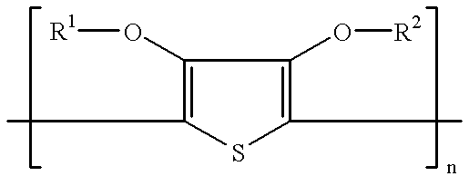
(a) a polythiophene with formula
Figure US06340496-20020122-C00001
wherein each of R1 and R2 independently represents hydrogen or a C1-4 alkyl group or together represent an optionally substituted C1-4 alkylene group or a cycloalkylene group, preferably an ethylene group, an optionally alkyl-substituted methylene group, an optionally C1-12 alkyl- or phenyl-substituted 1,2-ethylene group, a 1,3-propylene group or a 1,2-cyclohexylene group,
(b) a polyanion compound and
(c) an organic compound containing 2 or more OH and/or COOH groups or amide or lactam groups. Such layers have been described in EP-A-686 662.
The printing can proceed on layers containing of a polyethylene-di-oxythiophene, polystyrenesulphonic acid wherein between 10 and 5000 mg/m2 of the polythiophene is present, preferably layers wherein between 50 and 1000 mg/m2 of the polythiophene is present are used and more preferably layers wherein between 75 and 500 mg/m2 of the polythiophene is present are used. The layers comprising a conductive polymer and printed in the method of this invention can have any conductivity. The method of this invention can, e.g., be used to pattern layers with conductivity between 1 and 105 S/cm. Preferably the conductive layers patterned by the method of this invention have conductivity between 5 and 104 S/cm, more preferably between 10 and 1000 S/cm.
EXAMPLES 1 Preparation of the Polythiophene Dispersion (PT) (Hereinafter Called Dispersion PT)
a) Into 1000 ml of an aqueous solution of 14 g of polystyrene sulphonic acid (218 mmol of SO3H groups) with number-average molecular weight (Mn) 40,000, were introduced 12.9 g of potassium peroxodisulfate (K2S2O8), 0.1 g of Fe2 (SO4)3 and 5.68 g of 3,4-ethylenedioxy-thiophene. The thus obtained reaction mixture was stirred for 24 h at 20° C. and subjected to desalting.
b) 500 ml of the above prepared reaction mixture were diluted with 500 ml of water and stirred for 6 hours at room temperature in the presence of a granulated weak basic ion exchange resin LEWATIT H 600 (trade name of Bayer AG, Leverkusen, Germany) and strongly acidic ion exchanger LEWATIT S 100 (trade name of Bayer AG, Leverkusen, Germany). After said treatment the ion exchange resins were filtered off and the potassium ion and sulfate ion content were measured which were respectively 0.4 g K+ and 0.1 g (SO4)2− per liter.
Example 1
417 ml of dispersion PT and 50 g of methylpyrrolidone (compound A) were mixed with a binder (8.5 ml of a 30 % dispersion of co(vinylidenechloride/methylacrylate/itaconic acid 88/10/2) and a surfactant (0.5 ml of FLUORAD FC430, trade name of 3M) and the mixture was brought to 1000 ml with distilled water.
This mixture was coated on a 100 μm thick polyethyleneterephthalate film whereon a subbing layer (as usual on supports for photographic material) was present. The mixture was coated at a wet thickness of 40 mμ, and dried at a temperature of 35° C.
The dried layer contained 200 mg/m2 of polythiophene.
The resistivity in Ω/square was measured as described above and was 680 Ω/square.
Printing Example 1
On the layer a pattern was printed with screen-printing using a printing solution containing ClO so that 25 mg/m2 of NaClO was present. After printing the printing solution was washed away. The conductivity of the printed pattern was 1011 times lower than the conductivity of the conductive layer.
Printing Example 2
On the layer a pattern was printed with screen-printing using a printing solution containing MnO4 at pH=3, so that 667 mg/m2 of KMnO4 was present. After printing the printing solution was washed away. The conductivity of the printed pattern was 107 times lower than the conductivity of the conductive layer.
Printing Example 3
On the layer a pattern was printed with screen-printing using a printing solution containing MnO4 at pH=10, so that 667 mg/m2 of KMnO4 was present. After printing the printing solution was washed away. The conductivity of the printed pattern was 107 times lower than the conductivity of the conductive layer.
Printing Example 4
On the layer a pattern was printed with screen printing using a printing solution containing (NH4)2S2O8 at pH=10, so that 125 mg/m2 of (NH4)2S2O8 was present. After printing the printing solution was washed away. The conductivity of the printed pattern was 106 times lower than the conductivity of the conductive layer
Printing Example 5
On the layer a pattern was printed with screen printing using a printing solution containing (NH4)2S2O8 at pH=2.6, so that 125 mg/m2 of (NH4)2S2O8 was present. After printing the printing solution was washed away. The conductivity of the printed pattern was 103 times lower than the conductivity of the conductive layer
Printing Example 6
On the layer a pattern was printed with screen-printing using a printing solution containing KIO3 at pH=2, so that 1250 mg/m2 of KIO3 was present. After printing the printing solution was washed away. The conductivity of the printed pattern was only 4 times lower than the conductivity of the conductive layer. Thus this oxidant is not useful in the method of this invention.

Claims (7)

What is claimed is:
1. A method for producing electrode pattern in a conductive polymer on a substrate comprising the steps of
applying a layer containing between 10 and 5000 mg/m2 of a conductive polymer, so as to prepare a conductive layer and
printing an electrode pattern on said layer using a printing solution containing of an oxidant selected from the group consisting of ClO, BrO, MnO4 , Cr2O7 −−, S2O8 −− and H2O2.
2. A method according to claim 1, wherein said conductive layer has a conductivity between 1 and 105 S/cm.
3. A method according to claim 1, wherein said conductive polymer has formula:
Figure US06340496-20020122-C00002
in which, each of R1 and R2 independently represents hydrogen or a C1-4 alkyl group or together represent a C1-4 alkylene group or a cycloalkylene group, preferably an ethylene group, a methylene group, a C1-12 1,2-ethylene group, a 1,3-propylene group or a 1,2-cyclohexylene group.
4. A method according to claim 3, wherein said conductive polymer is applied from an aqueous solution containing a polyanion compound.
5. A method according to claim 1, wherein said printing proceeds by a printing method selected from the group consisting of offset printing, screen printing and ink-jet printing.
6. A method according to claim 1, wherein said printing proceeds so as to apply between 25 and 800 mg/m2 of oxidant.
7. A method according claim 1, wherein said printing solution comprises a thickener selected from the group consisting of silica, silicates, clay, synthetic clay and polymeric thickeners.
US09/573,549 1999-05-20 2000-05-19 Method for patterning a layer of conductive polymers Expired - Lifetime US6340496B1 (en)

Priority Applications (1)

Application Number Priority Date Filing Date Title
US09/573,549 US6340496B1 (en) 1999-05-20 2000-05-19 Method for patterning a layer of conductive polymers

Applications Claiming Priority (4)

Application Number Priority Date Filing Date Title
EP99201645A EP1054414B1 (en) 1999-05-20 1999-05-20 Method for patterning a layer of conductive polymer
EP99201645 1999-05-20
US13727599P 1999-06-01 1999-06-01
US09/573,549 US6340496B1 (en) 1999-05-20 2000-05-19 Method for patterning a layer of conductive polymers

Publications (1)

Publication Number Publication Date
US6340496B1 true US6340496B1 (en) 2002-01-22

Family

ID=27240095

Family Applications (1)

Application Number Title Priority Date Filing Date
US09/573,549 Expired - Lifetime US6340496B1 (en) 1999-05-20 2000-05-19 Method for patterning a layer of conductive polymers

Country Status (1)

Country Link
US (1) US6340496B1 (en)

Cited By (20)

* Cited by examiner, † Cited by third party
Publication number Priority date Publication date Assignee Title
US20030213624A1 (en) * 2002-05-20 2003-11-20 Cross Elisa M. Capacitive touch screen with conductive polymer
US20030222250A1 (en) * 2002-02-28 2003-12-04 Che-Hsiung Hsu Polymer buffer layers and their use in light-emitting diodes
WO2004029128A2 (en) * 2002-09-24 2004-04-08 E.I. Du Pont De Nemours And Company Water dispersible polythiophenes made with polymeric acid colloids
US20040254297A1 (en) * 2003-04-22 2004-12-16 Che-Hsiung Hsu Water dispersible polythiophenes made with polymeric acid colloids
US20070004899A1 (en) * 2003-09-24 2007-01-04 Che-Hsiung Hsu Water dispersible polythiophenes made with polymeric acid colloids
US20080035736A1 (en) * 2004-09-17 2008-02-14 Ovd Kinegram Ag Security Document With Electrically-Controlled Display Element
US20080210909A1 (en) * 2006-12-28 2008-09-04 Che-Hsiung Hsu Compositions of polyaniline made with perfuoropolymeric acid which are heat-enhanced and electronic devices made therewith
US20080213594A1 (en) * 2006-12-28 2008-09-04 Che-Hsiung Hsu Laser (230nm) ablatable compositions of electrically conducting polymers made with a perfluoropolymeric acid applications thereof
US20090072201A1 (en) * 2002-09-24 2009-03-19 E. I. Du Pont De Nemours And Company Water dispersible polyanilines made with polymeric acid colloids for electronics applications
CN100524049C (en) * 2003-08-26 2009-08-05 伊斯曼柯达公司 Electrographic patterning of conductive electrode layers
US20090213285A1 (en) * 2008-02-21 2009-08-27 Samsung Electronics Co., Ltd. Display device and method of manufacturing the same
US7670506B1 (en) 2004-12-30 2010-03-02 E. I. Du Pont De Nemours And Company Photoactive compositions for liquid deposition
US20100089872A1 (en) * 2006-09-29 2010-04-15 Tsurumi Soda Co., Ltd. Etching liquid for conductive polymer, and method for patterning conductive polymer
US20100263246A1 (en) * 2007-11-07 2010-10-21 Sang Keun Oh Transparent signboard and fabricating method thereof
US7837901B2 (en) 2005-06-27 2010-11-23 E. I. Du Pont De Nemours And Company Electrically conductive polymer compositions
US20110117329A1 (en) * 2007-08-29 2011-05-19 H.C. Starck Clevios Gmbh Production of conductive coatings by means of inkjet printing
US20110168952A1 (en) * 2006-12-29 2011-07-14 E. I. Du Pont De Nemours And Company High work-function and high conductivity compositions of electrically conducting polymers
US8409476B2 (en) 2005-06-28 2013-04-02 E I Du Pont De Nemours And Company High work function transparent conductors
US8699208B2 (en) 2005-09-13 2014-04-15 Heraeus Precious Metals Gmbh & Co. Kg Process for the production of electrolyte capacitors
US8765022B2 (en) 2004-03-17 2014-07-01 E I Du Pont De Nemours And Company Water dispersible polypyrroles made with polymeric acid colloids for electronics applications

Citations (7)

* Cited by examiner, † Cited by third party
Publication number Priority date Publication date Assignee Title
US4699804A (en) * 1984-12-28 1987-10-13 Hoechst Gosei Kabushiki Kaisha Process for producing electrically conductive composite polymer article
US4959430A (en) 1988-04-22 1990-09-25 Bayer Aktiengesellschaft Polythiophenes, process for their preparation and their use
EP0615256A2 (en) 1993-03-09 1994-09-14 Koninklijke Philips Electronics N.V. Method of manufacturing a pattern of an electrically conductive polymer on a substrate surface and method of metallizing such a pattern
US5561030A (en) * 1991-05-30 1996-10-01 Simon Fraser University Fabrication of electronically conducting polymeric patterns
WO1997018944A1 (en) 1995-11-22 1997-05-29 The Government Of The United States Of America, Represented By The Secretary Of The Navy Patterned conducting polymer surfaces and process for preparing the same and devices containing the same
US5766515A (en) * 1994-05-06 1998-06-16 Bayer Aktiengessellschaft Conductive coatings
EP1079397A1 (en) * 1999-08-23 2001-02-28 Agfa-Gevaert N.V. Method of making an electroconductive pattern on a support

Patent Citations (7)

* Cited by examiner, † Cited by third party
Publication number Priority date Publication date Assignee Title
US4699804A (en) * 1984-12-28 1987-10-13 Hoechst Gosei Kabushiki Kaisha Process for producing electrically conductive composite polymer article
US4959430A (en) 1988-04-22 1990-09-25 Bayer Aktiengesellschaft Polythiophenes, process for their preparation and their use
US5561030A (en) * 1991-05-30 1996-10-01 Simon Fraser University Fabrication of electronically conducting polymeric patterns
EP0615256A2 (en) 1993-03-09 1994-09-14 Koninklijke Philips Electronics N.V. Method of manufacturing a pattern of an electrically conductive polymer on a substrate surface and method of metallizing such a pattern
US5766515A (en) * 1994-05-06 1998-06-16 Bayer Aktiengessellschaft Conductive coatings
WO1997018944A1 (en) 1995-11-22 1997-05-29 The Government Of The United States Of America, Represented By The Secretary Of The Navy Patterned conducting polymer surfaces and process for preparing the same and devices containing the same
EP1079397A1 (en) * 1999-08-23 2001-02-28 Agfa-Gevaert N.V. Method of making an electroconductive pattern on a support

Cited By (39)

* Cited by examiner, † Cited by third party
Publication number Priority date Publication date Assignee Title
US6955773B2 (en) * 2002-02-28 2005-10-18 E.I. Du Pont De Nemours And Company Polymer buffer layers and their use in light-emitting diodes
US20030222250A1 (en) * 2002-02-28 2003-12-04 Che-Hsiung Hsu Polymer buffer layers and their use in light-emitting diodes
US7477242B2 (en) * 2002-05-20 2009-01-13 3M Innovative Properties Company Capacitive touch screen with conductive polymer
US20030213624A1 (en) * 2002-05-20 2003-11-20 Cross Elisa M. Capacitive touch screen with conductive polymer
US20040102577A1 (en) * 2002-09-24 2004-05-27 Che-Hsiung Hsu Water dispersible polythiophenes made with polymeric acid colloids
US8318046B2 (en) 2002-09-24 2012-11-27 E I Du Pont De Nemours And Company Water dispersible polyanilines made with polymeric acid colloids for electronics applications
WO2004029128A3 (en) * 2002-09-24 2004-05-27 Du Pont Water dispersible polythiophenes made with polymeric acid colloids
US20080296536A1 (en) * 2002-09-24 2008-12-04 Che-Hsiung Hsu Water dispersible polythiophenes made with polymeric acid colloids
US8585931B2 (en) 2002-09-24 2013-11-19 E I Du Pont De Nemours And Company Water dispersible polythiophenes made with polymeric acid colloids
US20090072201A1 (en) * 2002-09-24 2009-03-19 E. I. Du Pont De Nemours And Company Water dispersible polyanilines made with polymeric acid colloids for electronics applications
US8784692B2 (en) 2002-09-24 2014-07-22 E I Du Pont De Nemours And Company Water dispersible polythiophenes made with polymeric acid colloids
WO2004029128A2 (en) * 2002-09-24 2004-04-08 E.I. Du Pont De Nemours And Company Water dispersible polythiophenes made with polymeric acid colloids
US7431866B2 (en) 2002-09-24 2008-10-07 E. I. Du Pont De Nemours And Company Water dispersible polythiophenes made with polymeric acid colloids
US8641926B2 (en) 2003-04-22 2014-02-04 E I Du Pont De Nemours And Company Water dispersible polythiophenes made with polymeric acid colloids
US20080248314A1 (en) * 2003-04-22 2008-10-09 Che-Hsiung Hsu Water dispersible polythiophenes made with polymeric acid colloids
US7390438B2 (en) 2003-04-22 2008-06-24 E.I. Du Pont De Nemours And Company Water dispersible substituted polydioxythiophenes made with fluorinated polymeric sulfonic acid colloids
US20040254297A1 (en) * 2003-04-22 2004-12-16 Che-Hsiung Hsu Water dispersible polythiophenes made with polymeric acid colloids
CN100524049C (en) * 2003-08-26 2009-08-05 伊斯曼柯达公司 Electrographic patterning of conductive electrode layers
US20070004899A1 (en) * 2003-09-24 2007-01-04 Che-Hsiung Hsu Water dispersible polythiophenes made with polymeric acid colloids
US8765022B2 (en) 2004-03-17 2014-07-01 E I Du Pont De Nemours And Company Water dispersible polypyrroles made with polymeric acid colloids for electronics applications
US8387886B2 (en) * 2004-09-17 2013-03-05 Ovd Kinegram Ag Security document with electrically-controlled display element
US20080035736A1 (en) * 2004-09-17 2008-02-14 Ovd Kinegram Ag Security Document With Electrically-Controlled Display Element
US7670506B1 (en) 2004-12-30 2010-03-02 E. I. Du Pont De Nemours And Company Photoactive compositions for liquid deposition
US20110031441A1 (en) * 2005-06-27 2011-02-10 E.I. Du Pont De Nemours And Company Dupont Display Inc Electrically conductive polymer compositions
US7837901B2 (en) 2005-06-27 2010-11-23 E. I. Du Pont De Nemours And Company Electrically conductive polymer compositions
US8568616B2 (en) 2005-06-27 2013-10-29 E I Du Pont De Nemours And Company Electrically conductive polymer compositions
US8409476B2 (en) 2005-06-28 2013-04-02 E I Du Pont De Nemours And Company High work function transparent conductors
US8699208B2 (en) 2005-09-13 2014-04-15 Heraeus Precious Metals Gmbh & Co. Kg Process for the production of electrolyte capacitors
US20100089872A1 (en) * 2006-09-29 2010-04-15 Tsurumi Soda Co., Ltd. Etching liquid for conductive polymer, and method for patterning conductive polymer
US8153029B2 (en) 2006-12-28 2012-04-10 E.I. Du Pont De Nemours And Company Laser (230NM) ablatable compositions of electrically conducting polymers made with a perfluoropolymeric acid applications thereof
US8062553B2 (en) 2006-12-28 2011-11-22 E. I. Du Pont De Nemours And Company Compositions of polyaniline made with perfuoropolymeric acid which are heat-enhanced and electronic devices made therewith
US20080213594A1 (en) * 2006-12-28 2008-09-04 Che-Hsiung Hsu Laser (230nm) ablatable compositions of electrically conducting polymers made with a perfluoropolymeric acid applications thereof
US20080210909A1 (en) * 2006-12-28 2008-09-04 Che-Hsiung Hsu Compositions of polyaniline made with perfuoropolymeric acid which are heat-enhanced and electronic devices made therewith
US8491819B2 (en) 2006-12-29 2013-07-23 E I Du Pont De Nemours And Company High work-function and high conductivity compositions of electrically conducting polymers
US20110168952A1 (en) * 2006-12-29 2011-07-14 E. I. Du Pont De Nemours And Company High work-function and high conductivity compositions of electrically conducting polymers
US20110117329A1 (en) * 2007-08-29 2011-05-19 H.C. Starck Clevios Gmbh Production of conductive coatings by means of inkjet printing
US20100263246A1 (en) * 2007-11-07 2010-10-21 Sang Keun Oh Transparent signboard and fabricating method thereof
US20090213285A1 (en) * 2008-02-21 2009-08-27 Samsung Electronics Co., Ltd. Display device and method of manufacturing the same
US9373651B2 (en) 2008-02-21 2016-06-21 Samsung Display Co., Ltd. Display device and method of manufacturing the same

Similar Documents

Publication Publication Date Title
EP1054414B1 (en) Method for patterning a layer of conductive polymer
US6340496B1 (en) Method for patterning a layer of conductive polymers
US6444400B1 (en) Method of making an electroconductive pattern on a support
KR100594550B1 (en) Printed Conductors Made of Polyalkylene Dioxythiophene
EP1444710B1 (en) Thin film capacitor using conductive polymers
CN101023138B (en) Conductive composition and process for production thereof, antistatic coating material, antistatic membrane, antistatic film, optical filter, optical information recording media, and condenser and pro
EP1658650B1 (en) Forming electrically conductive layers by ink printing
KR101075264B1 (en) Water dispersible polythiophenes made with polymeric acid colloids
CN101679714B (en) Hole injection/transport layer compositions and devices
US20060062983A1 (en) Coatable conductive polyethylenedioxythiophene with carbon nanotubes
EP1003179B1 (en) A method for preparing a conductive polythiophene layer at low temperature
EP1079397A1 (en) Method of making an electroconductive pattern on a support
US20070059901A1 (en) Metal and electronically conductive polymer transfer
EP1546238A1 (en) Methods for directly producing stable aqueous dispersions of electrically conducting polyanilines
EP1456856B1 (en) Material for making a conductive pattern
KR20130087368A (en) Ink for conductive polymer etching and method for patterning conductive polymer
DE69919661T2 (en) Process for the preparation of a layer of conductive polythiophene at low temperature
WO2008002481A1 (en) Conductive polymer coating with improved aging stability
CN104570423A (en) Display substrate, manufacturing method of display substrate, display panel and display device
JPH0124236B2 (en)
CN1514449A (en) Electric resistance material
JP2000162421A (en) Color filter

Legal Events

Date Code Title Description
AS Assignment

Owner name: AGFA-GEVAERT, BELGIUM

Free format text: ASSIGNMENT OF ASSIGNORS INTEREST;ASSIGNORS:CLOOTS, TOM;VAN DEN BOGAERT, ROGER;TAHON, JEAN-PIERRE;AND OTHERS;REEL/FRAME:012208/0036

Effective date: 20000606

FEPP Fee payment procedure

Free format text: PAYOR NUMBER ASSIGNED (ORIGINAL EVENT CODE: ASPN); ENTITY STATUS OF PATENT OWNER: LARGE ENTITY

STCF Information on status: patent grant

Free format text: PATENTED CASE

FPAY Fee payment

Year of fee payment: 4

FPAY Fee payment

Year of fee payment: 8

FPAY Fee payment

Year of fee payment: 12