US6344378B1 - Field effect transistors, field emission apparatuses, thin film transistors, and methods of forming field effect transistors - Google Patents

Field effect transistors, field emission apparatuses, thin film transistors, and methods of forming field effect transistors Download PDF

Info

Publication number
US6344378B1
US6344378B1 US09/260,231 US26023199A US6344378B1 US 6344378 B1 US6344378 B1 US 6344378B1 US 26023199 A US26023199 A US 26023199A US 6344378 B1 US6344378 B1 US 6344378B1
Authority
US
United States
Prior art keywords
gate
forming
layer
semiconductive
dielectric layer
Prior art date
Legal status (The legal status is an assumption and is not a legal conclusion. Google has not performed a legal analysis and makes no representation as to the accuracy of the status listed.)
Expired - Fee Related
Application number
US09/260,231
Inventor
Ji Ung Lee
John Lee
Benham Moradi
Current Assignee (The listed assignees may be inaccurate. Google has not performed a legal analysis and makes no representation or warranty as to the accuracy of the list.)
Micron Technology Inc
Original Assignee
Micron Technology Inc
Priority date (The priority date is an assumption and is not a legal conclusion. Google has not performed a legal analysis and makes no representation as to the accuracy of the date listed.)
Filing date
Publication date
Application filed by Micron Technology Inc filed Critical Micron Technology Inc
Priority to US09/260,231 priority Critical patent/US6344378B1/en
Assigned to MICRON TECHNOLOGY, INC. reassignment MICRON TECHNOLOGY, INC. ASSIGNMENT OF ASSIGNORS INTEREST (SEE DOCUMENT FOR DETAILS). Assignors: LEE, JI UNG, MORADI, BENHAM, LEE, JOHN
Priority to US09/678,468 priority patent/US6504170B1/en
Application granted granted Critical
Priority to US10/072,415 priority patent/US7329552B2/en
Publication of US6344378B1 publication Critical patent/US6344378B1/en
Anticipated expiration legal-status Critical
Expired - Fee Related legal-status Critical Current

Links

Images

Classifications

    • HELECTRICITY
    • H01ELECTRIC ELEMENTS
    • H01LSEMICONDUCTOR DEVICES NOT COVERED BY CLASS H10
    • H01L29/00Semiconductor devices adapted for rectifying, amplifying, oscillating or switching, or capacitors or resistors with at least one potential-jump barrier or surface barrier, e.g. PN junction depletion layer or carrier concentration layer; Details of semiconductor bodies or of electrodes thereof  ; Multistep manufacturing processes therefor
    • H01L29/66Types of semiconductor device ; Multistep manufacturing processes therefor
    • H01L29/68Types of semiconductor device ; Multistep manufacturing processes therefor controllable by only the electric current supplied, or only the electric potential applied, to an electrode which does not carry the current to be rectified, amplified or switched
    • H01L29/76Unipolar devices, e.g. field effect transistors
    • H01L29/772Field effect transistors
    • H01L29/78Field effect transistors with field effect produced by an insulated gate
    • H01L29/786Thin film transistors, i.e. transistors with a channel being at least partly a thin film
    • H01L29/78606Thin film transistors, i.e. transistors with a channel being at least partly a thin film with supplementary region or layer in the thin film or in the insulated bulk substrate supporting it for controlling or increasing the safety of the device
    • H01L29/78618Thin film transistors, i.e. transistors with a channel being at least partly a thin film with supplementary region or layer in the thin film or in the insulated bulk substrate supporting it for controlling or increasing the safety of the device characterised by the drain or the source properties, e.g. the doping structure, the composition, the sectional shape or the contact structure
    • HELECTRICITY
    • H01ELECTRIC ELEMENTS
    • H01JELECTRIC DISCHARGE TUBES OR DISCHARGE LAMPS
    • H01J9/00Apparatus or processes specially adapted for the manufacture, installation, removal, maintenance of electric discharge tubes, discharge lamps, or parts thereof; Recovery of material from discharge tubes or lamps
    • H01J9/02Manufacture of electrodes or electrode systems
    • H01J9/022Manufacture of electrodes or electrode systems of cold cathodes
    • H01J9/025Manufacture of electrodes or electrode systems of cold cathodes of field emission cathodes
    • HELECTRICITY
    • H01ELECTRIC ELEMENTS
    • H01JELECTRIC DISCHARGE TUBES OR DISCHARGE LAMPS
    • H01J2201/00Electrodes common to discharge tubes
    • H01J2201/30Cold cathodes
    • H01J2201/319Circuit elements associated with the emitters by direct integration

Definitions

  • the present invention relates to field effect transistors, field emission apparatuses, thin film transistors, and methods of forming field effect transistors.
  • Field effect transistors are well known in the art. Such transistors are utilized in a variety of applications.
  • One exemplary field effect transistor configuration is the thin film transistor. Thin film transistor configurations have been particularly useful in field emission devices, such as field emission displays.
  • thin film field effect transistors are formed over an insulative substrate, such as glass.
  • a thin film semiconductive layer is formed over the insulative substrate.
  • An exemplary semiconductive layer comprises amorphous silicon.
  • a gate dielectric layer and gate layer are provided over the thin film layer and patterned using photolithography to form a gate. Conductive regions are formed intrinsically using plasma enhanced chemical vapor deposition (PECVD) with appropriate gas precursors to form the thin film field effect transistor construction.
  • PECVD plasma enhanced chemical vapor deposition
  • the present invention provides field effect transistors, field emission apparatuses, thin film transistors, and methods of forming field effect transistors.
  • a field effect transistor includes a semiconductive layer configured to form a channel region.
  • the field effect transistor further includes a pair of spaced conductively doped regions in electrical connection with the channel region of the semiconductive layer and a gate intermediate the semiconductive regions.
  • a gate dielectric layer is provided intermediate the semiconductive layer and the gate, and the gate dielectric layer is configured to align the gate with the channel region of the semiconductive layer.
  • the conductive regions comprise source/drain regions.
  • One of the source/drain regions may be formed to comprise a field emitter providing a field emission apparatus.
  • the field emission apparatus is configured as an active field device in some configurations.
  • a field emission device includes a transistor configured to control the emission of electrons from an emitter.
  • Yet another aspect of the present invention provides a method of forming a field effect transistor.
  • the method includes the steps of forming a semiconductive layer having a channel region and forming plural spaced conductively doped regions electrically coupled with the semiconductive layer.
  • This method further provides forming a gate dielectric layer over the semiconductive layer, forming a gate over the gate dielectric layer, and aligning the gate with the channel region using the gate dielectric layer.
  • FIG. 1 is a cross-sectional view of a segment of a thin film field effect transistor at a preliminary processing step.
  • FIG. 2 is a plan view of the segment shown in FIG. 1 .
  • FIG. 3 is a cross-sectional view of the segment shown in FIG. 1 at a subsequent processing step.
  • FIG. 4 is a cross-sectional view of the segment shown in FIG. 3 at a subsequent processing step.
  • FIG. 5 is a cross-sectional view of the segment shown in FIG. 4 at a subsequent processing step.
  • FIG. 6 is a plan view of the segment shown in FIG. 5 .
  • FIG. 7 is a cross-sectional view of the segment shown in FIG. 5 at a subsequent processing step.
  • FIG. 8 is a cross-sectional view of the segment shown in FIG. 7 at a subsequent processing step.
  • FIG. 9 is a plan view of the segment shown in FIG. 8 .
  • FIG. 10 is a cross-sectional view of the segment comprising a thin film field effect transistor.
  • FIG. 11 is a plan view of the thin film field effect transistor shown in FIG. 10 .
  • FIG. 12 is a cross-sectional view of a segment comprising an alternative thin film field effect transistor configuration.
  • FIG. 13 is a cross-sectional view of a segment showing processing of a field emission device at a preliminary processing step.
  • FIG. 14 is a cross-sectional view of the segment shown in FIG. 13 at a subsequent processing step.
  • FIG. 15 is a cross-sectional view of the segment shown in FIG. 14 at a subsequent processing step.
  • FIG. 16 is a cross-sectional view of the segment comprising a field emission device.
  • FIG. 17 is a cross-sectional view of a segment of an alternative field emission device.
  • the present invention discloses transistors and methods of forming transistors.
  • An exemplary transistor of the present invention includes a thin film transistor (TFT) having a semiconductor-on-insulator (SOI) construction.
  • TFT thin film transistor
  • SOI semiconductor-on-insulator
  • FIG. 12 A second thin film field effect transistor configuration according to the present invention is depicted in FIG. 12 .
  • Fabrication of another thin film field effect transistor arrangement including a field emitter is described herein with reference to FIG. 13 -FIG. 16 .
  • the configuration depicted in FIG. 16 comprises an active switching field emission device.
  • Segment 10 includes an insulative substrate 12 and a semiconductive layer 14 formed over insulative substrate 12 .
  • Exemplary materials for insulative substrate 12 include glass, sapphire or silicon oxide.
  • Semiconductive layer 14 is preferably formed as a thin film semiconductive layer having an approximate height or thickness of 0.2-0.5 microns.
  • Thin film semiconductive layer 14 comprises amorphous silicon according to the described embodiment although other materials may be utilized, such as SiC, CdSe, polycrystalline Si, microcrystalline Si, etc.
  • Thin film semiconductive layer 14 is ideally doped to provide increased conductivity.
  • thin film semiconductive layer 14 is doped with a p-type impurity using intrinsic doping.
  • thin film conductive layer 14 is configured to form a channel region 15 of a field effect transistor to selectively conduct electrons between adjacent semiconductive regions (shown in FIG. 5 ). Accordingly, at least a portion of layer 14 is provided intermediate the subsequently formed semiconductive regions.
  • Formation of thin film semiconductive layer 14 comprises providing a semiconductive layer over an upper surface of insulative substrate 12 , and subsequently patterning the layer to provide the configuration illustrated in FIG. 1 .
  • Conventional photolithography techniques are used in one embodiment to pattern the thin film semiconductive layer.
  • the patterned thin film semiconductive layer 14 forms a substantially rectangular shape in the presently described thin film field effect transistor configuration.
  • a semiconductive layer 16 is formed over insulative substrate 12 and patterned thin film semiconductive layer 14 .
  • Semiconductive layer 16 has an exemplary height or thickness of approximately 1-3 microns and is preferably doped to provide increased conductivity.
  • semiconductive layer 16 is preferably doped with an n+ type dopant to provide enhanced conductivity. Intrinsic doping using appropriate precursor gases are utilized in the described embodiment to dope layer 16 .
  • a patterned mask 18 is provided over semiconductive layer 16 .
  • Mask 18 permits subsequent processing of segment 10 in accordance with the present invention.
  • mask 18 comprises positive photoresist formed by photolithography. Individual portions of mask 18 individually have a length of approximately 10 microns.
  • portions of semiconductive layer 16 have been removed providing plural semiconductive regions 20 , 22 .
  • Semiconductive regions 20 , 22 correspond to mask 18 and may be formed by etching exposed portions of semiconductive layer 16 .
  • a largely isotropic silicon wet etch or plasma dry etch is utilized in one embodiment to etch layer 16 and form regions 20 , 22 .
  • semiconductive regions 20 , 22 are formed over and in electrical connection with thin film semiconductive layer 14 and channel region 15 thereof.
  • Channel region 15 generally extends intermediate semiconductive regions 20 , 22 .
  • Semiconductive regions 20 , 22 preferably comprise spaced conductively doped n+ regions. In the presently described embodiment, semiconductive regions 20 , 22 are formed as mesas.
  • Semiconductive regions 20 , 22 comprise source/drain regions of a field effect transistor. In typical applications, semiconductive regions 20 , 22 comprise a source region and drain region, respectively.
  • a gate dielectric layer 30 and gate layer 32 are formed over substrate 12 , semiconductive layer 14 , and semiconductive source/drain regions 20 , 22 .
  • Exemplary materials for layers 30 , 32 include silicon oxide and conductively doped polysilicon, respectively.
  • gate layer 32 is doped with an n+ dopant using plasma enhanced chemical vapor deposition (PECVD) techniques.
  • PECVD plasma enhanced chemical vapor deposition
  • Gate dielectric layer 30 has an exemplary height within the range of approximately 0.1-0.4 microns, and gate layer 32 has an exemplary thickness of approximately 0.2-0.5 microns.
  • gate dielectric layer 30 has a uniform thickness.
  • layers 30 , 32 are provided with a combined thickness “a” which does not exceed the individual heights “b” of semiconductive regions 20 , 22 . More specifically, semiconductive regions 20 , 22 comprise respective upper outermost surfaces 21 , 23 . Layer 32 includes an upper outermost surface 33 above channel region 15 . As referred to herein, upper outermost surfaces refer to surfaces away from or opposite insulative substrate 12 and thin film semiconductive layer 14 . Surfaces 21 , 23 are provided elevationally higher than surface 33 in the described embodiment. Surfaces 21 , 23 may be elevationally coincident or below surface 33 in other embodiments.
  • channel region 15 has a thickness less than the thickness of layer 32 . Accordingly, the height of region 15 and layer 30 have a combined thickness “c” less than a combined thickness “d” comprising layer 30 and layer 32 .
  • segment 10 is polished to remove portions of regions 20 , 22 and layers 30 , 32 .
  • the polishing comprises chemical-mechanical polishing according to the preferred embodiment. Respective uppermost surfaces or portions of semiconductive regions 20 , 22 are removed before removing any portions of gate dielectric layer 30 formed above a subsequently formed gate (having reference numeral 34 in FIG. 8 ). Polishing of segment 10 comprises initially polishing respective uppermost surfaces 21 , 23 of source/drain regions 20 , 22 before polishing any portions of gate layer 32 comprising surface 33 (surfaces 21 , 23 and 33 are shown in FIG. 7) above thin film channel region 15 . Surface 33 of gate layer 32 tends to act as a stopping position during polishing of fragment 10 .
  • a timed etch is used in an alternative fabrication method to remove portions of gate dielectric layer 30 , gate layer 32 and semiconductive regions 20 , 22 .
  • the processing step shown in FIG. 8 provides an isolated gate 34 intermediate semiconductive source/drain regions 20 , 22 .
  • Gate 34 is formed over and operatively proximate channel region 15 . More specifically, gate 34 is configured to control current flow intermediate semiconductive regions 20 , 22 through channel region 15 .
  • the described processing method for forming gate 34 includes removal of portions of gate dielectric layer 30 , gate layer 32 and semiconductive regions 20 , 22 in a common processing step.
  • gate 34 is formed without the use of a mask over gate material which subsequently forms gate 34 .
  • portions of both gate dielectric layer 30 and gate material layer 32 are removed using polishing or etching techniques as previously described without using a mask over the gate material which forms gate 34 .
  • Utilization of the described and preferred fabrication method provides a gate 34 which self-aligns with channel region 15 , and accomplishes such without any photomasking. Provision of gate dielectric layer 30 having a uniform thickness over thin film semiconductive layer 14 , and subsequent removal of portions of gate dielectric layer 30 and gate layer 32 operate to form and align gate 34 with channel region 15 . The preferred uniform thickness of gate dielectric layer 30 spaces gate 34 equally from semiconductive regions 20 , 22 and aligns gate 34 with channel region 15 .
  • gate 34 has an upper outermost surface 35 and semiconductive regions 20 , 22 have respective upper outermost surfaces 24 , 25 .
  • surface 35 comprises the same surface of gate layer 32 depicted with reference numeral 33 in FIG. 7 . Alternately, some polishing into layer 32 through surface 33 occurs.
  • Gate dielectric layer 30 includes upper outermost surfaces 31 following polishing of segment 10 . As illustrated, gate upper outermost surface 35 is substantially elevationally coincident with gate dielectric layer upper outermost surfaces 31 and surfaces 24 , 25 of respective semiconductive regions 20 , 22 .
  • portions of gate dielectric layer 30 and gate layer 32 located laterally outside of semiconductive regions 20 , 22 are preferably removed following the polishing of segment 10 as shown in FIG. 8.
  • a mask is formed over and intermediate semiconductive regions 20 , 22 according to one processing method of removing such external material of layers 30 , 32 . Thereafter, the external portions of layers 30 , 32 are etched or otherwise removed to provide the structure shown in FIG. 8 .
  • Thin film field effect transistor 38 formed upon segment 10 includes conductive material formed over gate 34 and source/drain regions 20 , 22 .
  • the conductive material forms plural source/drain electrodes 40 , 42 and a gate electrode 44 . Electrodes 40 , 42 , 44 are utilized to provide electrical connection of respective components of thin film field effect transistor 38 with external circuitry (not illustrated).
  • the conductive material comprises doped silicon or metal in exemplary embodiments.
  • segment 10 a includes an alternative thin film field effect transistor configuration 38 a .
  • Thin film field effect transistor 38 a of segment 10 a includes a conductive layer 17 intermediate insulative substrate 12 and semiconductive layer 14 a .
  • Formation of conductive layer 17 provides channel bias of region 15 .
  • Semiconductive layer 14 a has a reduced thickness compared with the semiconductive layer of previously described transistor configurations.
  • Semiconductive layer 14 a is provided over insulative substrate 12 and conductive layer 17 .
  • Conductive layer 17 is formed by chemical vapor deposition in one embodiment.
  • Segment 10 b of a field emission apparatus depicts the field emission apparatus at an intermediate processing step corresponding to the processing step of segment 10 illustrated in FIG. 5 and FIG. 6 .
  • Segment 10 b includes a thin film semiconductive layer 14 b having an increased lateral dimension over substrate 12 .
  • Source/drain regions 20 , 22 a over layer 14 b is shaped to form a field emitter 50 in accordance with the presently described embodiment. As illustrated, source/drain region 22 is formed as field emitter 50 .
  • Source/drain region 20 comprises a mesa similar to the previously described thin film field effect transistor configurations. Source/drain region 20 could be formed to comprise a field emitter and region 22 could be formed as a mesa in another embodiment.
  • Field emitter 50 can be formed utilizing a mask similar to the depicted mask 18 of FIG. 4 and having a reduced width. Utilization of a narrow mask provides source/drain region 22 a with a point which projects outwardly from substrate 12 and thin film semiconductive layer 14 b to form field emitter 50 .
  • One possible mask for fabricating field emitter 50 comprises a circular mask having a diameter of approximately 1 to 2 microns.
  • source/drain region 22 a comprising field emitter 50 is formed by a combination of isotropic and anisotropic etching of semiconductive layer 16 in plasma which contains fluorinated gas, such as NF 3 , in combination with a chlorinated gas, such as Cl 2 , and helium.
  • fluorinated gas such as NF 3
  • chlorinated gas such as Cl 2
  • helium a chlorinated gas
  • processing of segment 10 b occurs in a manner similar to the processing of the thin film field effect transistor previously described.
  • gate dielectric layer 30 and gate layer 32 are formed over semiconductive regions 20 , 22 a , substrate 12 and semiconductive layer 14 b .
  • the tip of field emitter 50 is preferably provided elevationally below the surface 33 of gate layer 32 and surface 21 of semiconductive region 20 .
  • segment 10 b has undergone polishing or other processing to remove portions of gate dielectric layer 30 , gate layer 32 and semiconductive region 20 .
  • polishing comprises chemical-mechanical polishing in the described embodiment and ceases prior to any polishing of field emitter 50 .
  • the removal of portions of layers 30 , 32 , and region 20 provides a gate 34 a aligned with channel region 15 intermediate semiconductive regions 20 , 22 a.
  • Field emission apparatus 60 comprises a thin film transistor including field emitter 50 .
  • external portions of gate dielectric layer 30 and gate layer 32 are preferably removed following the polishing of segment 10 b .
  • only the lateral portions of layers 30 , 32 adjacent and outwardly of semiconductive region 20 are removed in the preferred embodiment.
  • the external lateral portions of layers 30 , 32 adjacent the field emitter 50 are not removed according to one embodiment. More specifically, such lateral portions are utilized to provide an active field emission apparatus 60 .
  • the lateral portions provide a gate 34 a about field emitter 50 .
  • the depicted segment 10 b also includes a conductive material comprising electrodes 40 , 44 a over selected portions of the depicted thin film field emission apparatus 60 .
  • the conductive material can comprise doped silicon or metal in exemplary embodiments.
  • Electrodes 40 , 44 a are utilized to provide electrical connection with respective components of thin film field emission apparatus 60 with external circuitry (not illustrated). Such circuitry is configured in one embodiment to control the operation of field emission apparatus 60 .
  • Gate 34 a is configured to control current flow intermediate semiconductive region 20 and semiconductive region 22 a comprising field emitter 50 responsive to the selective application of a voltage potential via external circuitry (not shown) to gate 34 a .
  • Gate 34 a also controls the emission of electrons from field emitter 50 .
  • Cavity 36 is formed within gate dielectric layer 30 intermediate gate 34 a and semiconductive region 20 .
  • Cavity 37 is formed within gate dielectric layer 30 adjacent field emitter 50 .
  • Cavities 36 , 37 are formed by etching in the described embodiment.
  • An etchant is preferably chosen to permit etching of gate dielectric layer 30 with minimal or no etching of gate layer 32 (i.e., selective to gate layer 32 ) as illustrated.
  • Apparatus 60 a includes plural emitters 50 as shown. Emitters 50 are formed using the techniques previously described. A gate 34 b comprising material of layer 32 is provided about individual emitters 50 similar to the gate 34 a of FIG. 16 .
  • Electrodes 40 , 44 b comprising a conductive material such as doped silicon or metal are shown over portions of field emission apparatus 60 a . Electrodes 40 , 44 b are coupled with external circuitry (not shown) configured to control the operation of apparatus 60 a .
  • Gate 34 b is configured to control current flow intermediate region 20 and regions 22 a comprising field emitters 50 . As such, gate 34 b controls the emission of electrons from field emitters 50 .

Abstract

The present invention includes field effect transistors, field emission apparatuses, thin film transistors, and methods of forming field effect transistors. According to one embodiment, a field effect transistor includes a semiconductive layer configured to form a channel region; a pair of spaced conductively doped semiconductive regions in electrical connection with the channel region of the semiconductive layer; a gate intermediate the semiconductive regions; and a gate dielectric layer intermediate the semiconductive layer and the gate, the gate dielectric layer being configured to align the gate with the channel region of the semiconductive layer. In one aspect, chemical-mechanical polishing self-aligns the gate with the channel region. According to another aspect, a field emission device includes a transistor configured to control the emission of electrons from an emitter.

Description

TECHNICAL FIELD
The present invention relates to field effect transistors, field emission apparatuses, thin film transistors, and methods of forming field effect transistors.
BACKGROUND OF THE INVENTION
Field effect transistors are well known in the art. Such transistors are utilized in a variety of applications. One exemplary field effect transistor configuration is the thin film transistor. Thin film transistor configurations have been particularly useful in field emission devices, such as field emission displays.
In typical arrangements, thin film field effect transistors are formed over an insulative substrate, such as glass. A thin film semiconductive layer is formed over the insulative substrate. An exemplary semiconductive layer comprises amorphous silicon. A gate dielectric layer and gate layer are provided over the thin film layer and patterned using photolithography to form a gate. Conductive regions are formed intrinsically using plasma enhanced chemical vapor deposition (PECVD) with appropriate gas precursors to form the thin film field effect transistor construction.
Precise alignment of the gate with the active region of a field effect transistor, including thin film transistor configurations, is desired to ensure proper operation of the device as well as enhance the operational characteristics of the device. There exists a need in the art to provide improved field effect transistor device configurations and methodologies for fabricating such transistor devices for controlling emission.
SUMMARY OF THE INVENTION
The present invention provides field effect transistors, field emission apparatuses, thin film transistors, and methods of forming field effect transistors.
According to one aspect of the present invention a field effect transistor includes a semiconductive layer configured to form a channel region. The field effect transistor further includes a pair of spaced conductively doped regions in electrical connection with the channel region of the semiconductive layer and a gate intermediate the semiconductive regions. A gate dielectric layer is provided intermediate the semiconductive layer and the gate, and the gate dielectric layer is configured to align the gate with the channel region of the semiconductive layer.
According to some aspects of the present invention, the conductive regions comprise source/drain regions. One of the source/drain regions may be formed to comprise a field emitter providing a field emission apparatus. The field emission apparatus is configured as an active field device in some configurations.
In one aspect, chemical-mechanical polishing self-aligns the gate with the channel region. According to another aspect, a field emission device includes a transistor configured to control the emission of electrons from an emitter.
Yet another aspect of the present invention provides a method of forming a field effect transistor. The method includes the steps of forming a semiconductive layer having a channel region and forming plural spaced conductively doped regions electrically coupled with the semiconductive layer. This method further provides forming a gate dielectric layer over the semiconductive layer, forming a gate over the gate dielectric layer, and aligning the gate with the channel region using the gate dielectric layer.
Other aspects of the present invention are disclosed herein.
BRIEF DESCRIPTION OF THE DRAWINGS
Preferred embodiments of the invention are described below with reference to the following accompanying drawings.
FIG. 1 is a cross-sectional view of a segment of a thin film field effect transistor at a preliminary processing step.
FIG. 2 is a plan view of the segment shown in FIG. 1.
FIG. 3 is a cross-sectional view of the segment shown in FIG. 1 at a subsequent processing step.
FIG. 4 is a cross-sectional view of the segment shown in FIG. 3 at a subsequent processing step.
FIG. 5 is a cross-sectional view of the segment shown in FIG. 4 at a subsequent processing step.
FIG. 6 is a plan view of the segment shown in FIG. 5.
FIG. 7 is a cross-sectional view of the segment shown in FIG. 5 at a subsequent processing step.
FIG. 8 is a cross-sectional view of the segment shown in FIG. 7 at a subsequent processing step.
FIG. 9 is a plan view of the segment shown in FIG. 8.
FIG. 10 is a cross-sectional view of the segment comprising a thin film field effect transistor.
FIG. 11 is a plan view of the thin film field effect transistor shown in FIG. 10.
FIG. 12 is a cross-sectional view of a segment comprising an alternative thin film field effect transistor configuration.
FIG. 13 is a cross-sectional view of a segment showing processing of a field emission device at a preliminary processing step.
FIG. 14 is a cross-sectional view of the segment shown in FIG. 13 at a subsequent processing step.
FIG. 15 is a cross-sectional view of the segment shown in FIG. 14 at a subsequent processing step.
FIG. 16 is a cross-sectional view of the segment comprising a field emission device.
FIG. 17 is a cross-sectional view of a segment of an alternative field emission device.
DETAILED DESCRIPTION OF THE PREFERRED EMBODIMENTS
This disclosure of the invention is submitted in furtherance of the constitutional purposes of the U.S. Patent Laws “to promote the progress of science and useful arts” (Article 1, Section 8).
The present invention discloses transistors and methods of forming transistors. An exemplary transistor of the present invention includes a thin film transistor (TFT) having a semiconductor-on-insulator (SOI) construction. One fabrication method of the present invention for forming a first thin film field effect transistor configuration is described herein with reference to FIG. 1-FIG. 11. A second thin film field effect transistor configuration according to the present invention is depicted in FIG. 12. Fabrication of another thin film field effect transistor arrangement including a field emitter is described herein with reference to FIG. 13-FIG. 16. The configuration depicted in FIG. 16 comprises an active switching field emission device. Although the present invention is described with reference to thin film field effect transistors, the invention is not to be limited to such disclosed configurations.
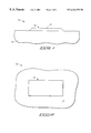
Referring to FIG. 1 and FIG. 2, a segment or fragment 10 of a thin film field effect transistor is illustrated. Segment 10 includes an insulative substrate 12 and a semiconductive layer 14 formed over insulative substrate 12. Exemplary materials for insulative substrate 12 include glass, sapphire or silicon oxide. Semiconductive layer 14 is preferably formed as a thin film semiconductive layer having an approximate height or thickness of 0.2-0.5 microns. Thin film semiconductive layer 14 comprises amorphous silicon according to the described embodiment although other materials may be utilized, such as SiC, CdSe, polycrystalline Si, microcrystalline Si, etc.
Thin film semiconductive layer 14 is ideally doped to provide increased conductivity. In one embodiment, thin film semiconductive layer 14 is doped with a p-type impurity using intrinsic doping. As described below, thin film conductive layer 14 is configured to form a channel region 15 of a field effect transistor to selectively conduct electrons between adjacent semiconductive regions (shown in FIG. 5). Accordingly, at least a portion of layer 14 is provided intermediate the subsequently formed semiconductive regions.
Formation of thin film semiconductive layer 14 comprises providing a semiconductive layer over an upper surface of insulative substrate 12, and subsequently patterning the layer to provide the configuration illustrated in FIG. 1. Conventional photolithography techniques are used in one embodiment to pattern the thin film semiconductive layer. As shown in FIG. 2, the patterned thin film semiconductive layer 14 forms a substantially rectangular shape in the presently described thin film field effect transistor configuration.
Referring to FIG. 3, a semiconductive layer 16 is formed over insulative substrate 12 and patterned thin film semiconductive layer 14. Semiconductive layer 16 has an exemplary height or thickness of approximately 1-3 microns and is preferably doped to provide increased conductivity. In the described embodiment, semiconductive layer 16 is preferably doped with an n+ type dopant to provide enhanced conductivity. Intrinsic doping using appropriate precursor gases are utilized in the described embodiment to dope layer 16.
Referring to FIG. 4, a patterned mask 18 is provided over semiconductive layer 16. Mask 18 permits subsequent processing of segment 10 in accordance with the present invention. In an exemplary embodiment, mask 18 comprises positive photoresist formed by photolithography. Individual portions of mask 18 individually have a length of approximately 10 microns.
Referring to FIG. 5 and FIG. 6, portions of semiconductive layer 16 have been removed providing plural semiconductive regions 20, 22. Semiconductive regions 20, 22 correspond to mask 18 and may be formed by etching exposed portions of semiconductive layer 16. A largely isotropic silicon wet etch or plasma dry etch is utilized in one embodiment to etch layer 16 and form regions 20, 22.
As illustrated, semiconductive regions 20, 22 are formed over and in electrical connection with thin film semiconductive layer 14 and channel region 15 thereof. Channel region 15 generally extends intermediate semiconductive regions 20, 22. Semiconductive regions 20, 22 preferably comprise spaced conductively doped n+ regions. In the presently described embodiment, semiconductive regions 20, 22 are formed as mesas.
Semiconductive regions 20, 22 comprise source/drain regions of a field effect transistor. In typical applications, semiconductive regions 20, 22 comprise a source region and drain region, respectively.
Referring to FIG. 7, a gate dielectric layer 30 and gate layer 32 are formed over substrate 12, semiconductive layer 14, and semiconductive source/ drain regions 20, 22. Exemplary materials for layers 30, 32 include silicon oxide and conductively doped polysilicon, respectively. In the described embodiment, gate layer 32 is doped with an n+ dopant using plasma enhanced chemical vapor deposition (PECVD) techniques. Gate dielectric layer 30 has an exemplary height within the range of approximately 0.1-0.4 microns, and gate layer 32 has an exemplary thickness of approximately 0.2-0.5 microns. Preferably, gate dielectric layer 30 has a uniform thickness.
In the illustrated embodiment, layers 30, 32 are provided with a combined thickness “a” which does not exceed the individual heights “b” of semiconductive regions 20, 22. More specifically, semiconductive regions 20, 22 comprise respective upper outermost surfaces 21, 23. Layer 32 includes an upper outermost surface 33 above channel region 15. As referred to herein, upper outermost surfaces refer to surfaces away from or opposite insulative substrate 12 and thin film semiconductive layer 14. Surfaces 21, 23 are provided elevationally higher than surface 33 in the described embodiment. Surfaces 21, 23 may be elevationally coincident or below surface 33 in other embodiments.
According to the preferred embodiment, channel region 15 has a thickness less than the thickness of layer 32. Accordingly, the height of region 15 and layer 30 have a combined thickness “c” less than a combined thickness “d” comprising layer 30 and layer 32.
Referring to FIG. 8 and FIG. 9, portions of gate dielectric layer 30, gate layer 32 and semiconductive regions 20, 22 have been removed. According to the described fabrication method, segment 10 is polished to remove portions of regions 20, 22 and layers 30, 32. The polishing comprises chemical-mechanical polishing according to the preferred embodiment. Respective uppermost surfaces or portions of semiconductive regions 20, 22 are removed before removing any portions of gate dielectric layer 30 formed above a subsequently formed gate (having reference numeral 34 in FIG. 8). Polishing of segment 10 comprises initially polishing respective uppermost surfaces 21, 23 of source/ drain regions 20, 22 before polishing any portions of gate layer 32 comprising surface 33 ( surfaces 21, 23 and 33 are shown in FIG. 7) above thin film channel region 15. Surface 33 of gate layer 32 tends to act as a stopping position during polishing of fragment 10.
A timed etch is used in an alternative fabrication method to remove portions of gate dielectric layer 30, gate layer 32 and semiconductive regions 20, 22.
The processing step shown in FIG. 8 provides an isolated gate 34 intermediate semiconductive source/ drain regions 20, 22. Gate 34 is formed over and operatively proximate channel region 15. More specifically, gate 34 is configured to control current flow intermediate semiconductive regions 20, 22 through channel region 15.
The described processing method for forming gate 34 includes removal of portions of gate dielectric layer 30, gate layer 32 and semiconductive regions 20, 22 in a common processing step. Preferably, gate 34 is formed without the use of a mask over gate material which subsequently forms gate 34. In particular, portions of both gate dielectric layer 30 and gate material layer 32 are removed using polishing or etching techniques as previously described without using a mask over the gate material which forms gate 34.
Utilization of the described and preferred fabrication method provides a gate 34 which self-aligns with channel region 15, and accomplishes such without any photomasking. Provision of gate dielectric layer 30 having a uniform thickness over thin film semiconductive layer 14, and subsequent removal of portions of gate dielectric layer 30 and gate layer 32 operate to form and align gate 34 with channel region 15. The preferred uniform thickness of gate dielectric layer 30 spaces gate 34 equally from semiconductive regions 20, 22 and aligns gate 34 with channel region 15.
Still referring to FIG. 8, gate 34 has an upper outermost surface 35 and semiconductive regions 20, 22 have respective upper outermost surfaces 24, 25. In some instances, surface 35 comprises the same surface of gate layer 32 depicted with reference numeral 33 in FIG. 7. Alternately, some polishing into layer 32 through surface 33 occurs.
Surfaces 24, 25 are elevationally lower than surfaces 21, 23 shown in FIG. 7 due to polishing of segment 10 according to the described fabrication method. Gate dielectric layer 30 includes upper outermost surfaces 31 following polishing of segment 10. As illustrated, gate upper outermost surface 35 is substantially elevationally coincident with gate dielectric layer upper outermost surfaces 31 and surfaces 24, 25 of respective semiconductive regions 20, 22.
Although such step is not depicted, portions of gate dielectric layer 30 and gate layer 32 located laterally outside of semiconductive regions 20, 22 are preferably removed following the polishing of segment 10 as shown in FIG. 8. A mask is formed over and intermediate semiconductive regions 20, 22 according to one processing method of removing such external material of layers 30, 32. Thereafter, the external portions of layers 30, 32 are etched or otherwise removed to provide the structure shown in FIG. 8.
Referring to FIG. 10 and FIG. 11, one configuration of a thin film field effect transistor 38 is shown. Thin film field effect transistor 38 formed upon segment 10 includes conductive material formed over gate 34 and source/ drain regions 20, 22. The conductive material forms plural source/ drain electrodes 40, 42 and a gate electrode 44. Electrodes 40, 42, 44 are utilized to provide electrical connection of respective components of thin film field effect transistor 38 with external circuitry (not illustrated). The conductive material comprises doped silicon or metal in exemplary embodiments.
Referring to FIG. 12, another configuration of a thin film field effect transistor is depicted wherein like reference numerals represent like components with any substantial differences indicated by suffix “a”. The depicted segment 10 a includes an alternative thin film field effect transistor configuration 38 a. Thin film field effect transistor 38 a of segment 10 a includes a conductive layer 17 intermediate insulative substrate 12 and semiconductive layer 14 a. Formation of conductive layer 17 provides channel bias of region 15. Semiconductive layer 14 a has a reduced thickness compared with the semiconductive layer of previously described transistor configurations. Semiconductive layer 14 a is provided over insulative substrate 12 and conductive layer 17. Conductive layer 17 is formed by chemical vapor deposition in one embodiment.
Referring to FIG. 13, a segment 10 b of a field emission apparatus is illustrated. Segment 10 b of FIG. 13 depicts the field emission apparatus at an intermediate processing step corresponding to the processing step of segment 10 illustrated in FIG. 5 and FIG. 6. Segment 10 b includes a thin film semiconductive layer 14 b having an increased lateral dimension over substrate 12.
One of source/ drain regions 20, 22 a over layer 14 b is shaped to form a field emitter 50 in accordance with the presently described embodiment. As illustrated, source/drain region 22 is formed as field emitter 50. Source/drain region 20 comprises a mesa similar to the previously described thin film field effect transistor configurations. Source/drain region 20 could be formed to comprise a field emitter and region 22 could be formed as a mesa in another embodiment.
Field emitter 50 can be formed utilizing a mask similar to the depicted mask 18 of FIG. 4 and having a reduced width. Utilization of a narrow mask provides source/drain region 22 a with a point which projects outwardly from substrate 12 and thin film semiconductive layer 14 b to form field emitter 50. One possible mask for fabricating field emitter 50 comprises a circular mask having a diameter of approximately 1 to 2 microns.
In accordance with one fabrication method, source/drain region 22 a comprising field emitter 50 is formed by a combination of isotropic and anisotropic etching of semiconductive layer 16 in plasma which contains fluorinated gas, such as NF3, in combination with a chlorinated gas, such as Cl2, and helium. Such an etching process preferably provides field emitter 50 having an atomically sharp tip. Other fabrication techniques can also be utilized.
Referring to FIG. 14, following formation of semiconductive region 22 a as field emitter 50, processing of segment 10 b occurs in a manner similar to the processing of the thin film field effect transistor previously described. For example, gate dielectric layer 30 and gate layer 32 are formed over semiconductive regions 20, 22 a, substrate 12 and semiconductive layer 14 b. The tip of field emitter 50 is preferably provided elevationally below the surface 33 of gate layer 32 and surface 21 of semiconductive region 20.
Referring to FIG. 15, segment 10 b has undergone polishing or other processing to remove portions of gate dielectric layer 30, gate layer 32 and semiconductive region 20. Such polishing comprises chemical-mechanical polishing in the described embodiment and ceases prior to any polishing of field emitter 50. As previously described, the removal of portions of layers 30, 32, and region 20 provides a gate 34 a aligned with channel region 15 intermediate semiconductive regions 20, 22 a.
Referring to FIG. 16, segment 10 b having a field emission apparatus 60 thereon is illustrated. Field emission apparatus 60 comprises a thin film transistor including field emitter 50.
Similar to the previously described embodiment, external portions of gate dielectric layer 30 and gate layer 32 are preferably removed following the polishing of segment 10 b. However, only the lateral portions of layers 30, 32 adjacent and outwardly of semiconductive region 20 are removed in the preferred embodiment. The external lateral portions of layers 30, 32 adjacent the field emitter 50 are not removed according to one embodiment. More specifically, such lateral portions are utilized to provide an active field emission apparatus 60. The lateral portions provide a gate 34 a about field emitter 50.
The depicted segment 10 b also includes a conductive material comprising electrodes 40, 44 a over selected portions of the depicted thin film field emission apparatus 60. The conductive material can comprise doped silicon or metal in exemplary embodiments. Electrodes 40, 44 a are utilized to provide electrical connection with respective components of thin film field emission apparatus 60 with external circuitry (not illustrated). Such circuitry is configured in one embodiment to control the operation of field emission apparatus 60. Gate 34 a is configured to control current flow intermediate semiconductive region 20 and semiconductive region 22 a comprising field emitter 50 responsive to the selective application of a voltage potential via external circuitry (not shown) to gate 34 a. Gate 34 a also controls the emission of electrons from field emitter 50.
Cavity 36 is formed within gate dielectric layer 30 intermediate gate 34 a and semiconductive region 20. Cavity 37 is formed within gate dielectric layer 30 adjacent field emitter 50. Cavities 36, 37 are formed by etching in the described embodiment. An etchant is preferably chosen to permit etching of gate dielectric layer 30 with minimal or no etching of gate layer 32 (i.e., selective to gate layer 32) as illustrated.
Referring to FIG. 17, a segment 10 c having an alternative field emission apparatus 60 a thereon is illustrated. Apparatus 60 a includes plural emitters 50 as shown. Emitters 50 are formed using the techniques previously described. A gate 34 b comprising material of layer 32 is provided about individual emitters 50 similar to the gate 34 a of FIG. 16.
Electrodes 40, 44 b comprising a conductive material such as doped silicon or metal are shown over portions of field emission apparatus 60 a. Electrodes 40, 44 b are coupled with external circuitry (not shown) configured to control the operation of apparatus 60 a. Gate 34 b is configured to control current flow intermediate region 20 and regions 22 a comprising field emitters 50. As such, gate 34 b controls the emission of electrons from field emitters 50.
In compliance with the statute, the invention has been described in language more or less specific as to structural and methodical features. It is to be understood, however, that the invention is not limited to the specific features shown and described, since the means herein disclosed comprise preferred forms of putting the invention into effect. The invention is, therefore, claimed in any of its forms or modifications within the proper scope of the appended claims appropriately interpreted in accordance with the doctrine of equivalents.

Claims (48)

What is claimed is:
1. A method of forming a field effect transistor comprising:
forming a semiconductive layer having a channel region;
forming plural spaced conductively doped semiconductive regions electrically coupled with the semiconductive layer;
forming a gate dielectric layer over the semiconductive layer;
forming a gate over the gate dielectric layer; and
aligning the gate with the channel region using the gate dielectric layer.
2. The method according to claim 1 wherein the forming the semiconductive layer comprises forming a thin film semiconductive layer.
3. The method according to claim 1 wherein the forming and the aligning of the gate comprise forming a gate layer over the gate dielectric layer and removing portions of the gate dielectric layer and the gate layer.
4. The method according to claim 3 wherein the removing portions of the gate dielectric layer and the gate layer occur in a common processing step.
5. The method according to claim 3 wherein the removing comprises chemical-mechanical polishing.
6. The method according to claim 3 wherein the removing comprises initially removing respective uppermost surfaces of the semiconductive regions before removing any gate material above the gate.
7. The method according to claim 3 wherein the removing provides the gate dielectric layer with an upper outermost surface substantially elevationally coincident with an upper outermost surface of the gate.
8. The method according to claim 1 wherein the forming the gate comprises forming without using any mask.
9. The method according to claim 1 wherein the forming the gate comprises depositing gate material over the gate dielectric layer, and removing portions of the gate material without using a mask over the gate during the removing.
10. The method according to claim 1 wherein the forming the semiconductive regions comprises forming source and drain regions over the semiconductive layer.
11. The method according to claim 1 wherein the forming the semiconductive regions comprises forming a drain region comprising a field emitter.
12. The method according to claim 1 wherein the forming the semiconductive regions comprises forming a drain region comprising a plurality of field emitters.
13. A method of forming a field effect transistor comprising:
providing a semiconductive layer;
forming plural semiconductive regions electrically coupled with the semiconductive layer;
forming a gate dielectric layer over the semiconductive layer; and
forming a gate of gate material over the gate dielectric layer without the use of a mask over the gate material.
14. The method according to claim 13 further comprising aligning the gate with a channel region within the semiconductive layer using the gate dielectric layer.
15. The method according to claim 13 wherein the providing the semiconductive layer comprises forming a thin film semiconductive layer.
16. The method according to claim 13 wherein the forming the gate comprises removing portions of the gate dielectric layer and a gate layer in a common step.
17. The method according to claim 16 wherein the removing self-aligns the gate with a channel region within the semiconductive layer.
18. The method according to claim 16 wherein the removing comprises chemical-mechanical polishing.
19. The method according to claim 16 wherein the removing provides the gate dielectric layer with an upper outermost surface substantially elevationally coincident with an upper outermost surface of the gate.
20. The method according to claim 16 wherein the removing comprises initially removing respective uppermost surfaces of the semiconductive regions before removing any gate material above the gate.
21. The method according to claim 16 wherein the forming the semiconductive regions comprises forming a drain region comprising a field emitter.
22. The method according to claim 16 wherein the forming the semiconductive regions comprises forming a drain region comprising a plurality of field emitters.
23. A method of forming a field effect transistor comprising:
providing a semiconductive layer having a channel region;
providing plural semiconductive regions electrically coupled with the channel region;
forming a gate dielectric layer over the semiconductive layer; and
forming a gate of gate material comprising:
depositing the gate material over the gate dielectric layer;
removing portions of the gate material without using a mask over the gate during the removing.
24. The method according to claim 23 further comprising aligning the gate with the channel region using the gate dielectric layer.
25. The method according to claim 23 wherein the providing the semiconductive layer comprises forming a thin film semiconductive layer.
26. The method according to claim 23 wherein the removing comprises removing portions of the gate dielectric layer and the gate material in a common step.
27. The method according to claim 23 wherein the removing comprises chemical-mechanical polishing.
28. The method according to claim 23 wherein the removing provides the gate dielectric layer with an upper outermost surface substantially elevationally coincident with an upper outermost surface of the gate.
29. The method according to claim 23 wherein the removing comprises initially removing respective uppermost surfaces of the semiconductive regions before removing any gate material above the gate.
30. The method according to claim 23 wherein the providing the semiconductive regions comprises forming a drain region comprising a field emitter.
31. The method according to claim 23 wherein the providing the semiconductive regions comprises forming a drain region comprising a plurality of field emitters.
32. A method of forming a thin film transistor comprising:
forming a thin film semiconductive layer having a channel region;
providing plural semiconductive regions electrically coupled with the channel region;
forming a gate dielectric layer over the thin film semiconductive layer;
forming a gate layer over the gate dielectric layer; and
removing portions of the gate dielectric layer and the gate layer providing a gate self-aligned with the channel region.
33. The method according to claim 32 wherein the providing the semiconductive regions comprises forming a drain region comprising a field emitter.
34. The method according to claim 33 wherein the forming the gate layer comprises forming the gate layer about the field emitter.
35. The method according to claim 32 wherein the removing comprises chemical-mechanical polishing.
36. The method according to claim 32 wherein the removing provides the gate dielectric layer with an upper outermost surface substantially elevationally coincident with an upper outermost surface of the gate.
37. The method according to claim 32 wherein the removing comprises initially removing respective uppermost surfaces of the semiconductive regions before removing any gate material above the gate.
38. A method of forming a thin film transistor comprising:
forming source and drain regions having a thin film channel region positioned therebetween;
forming a gate layer and a gate dielectric layer over the thin film channel region; and
polishing the gate layer to form an isolated gate intermediate the source and drain regions over the thin film channel region.
39. The method according to claim 38 wherein the forming the gate layer comprises forming the gate layer over the source and drain regions.
40. The method according to claim 38 further comprising aligning the gate using the gate dielectric layer.
41. The method according to claim 38 wherein the forming the source and drain regions comprises forming the drain region as a field emitter.
42. The method according to claim 38 wherein the polishing comprises chemical-mechanical polishing.
43. The method according to claim 38 wherein the polishing provides the gate dielectric layer with an upper outermost surface substantially elevationally coincident with an upper outermost surface of the gate.
44. The method according to claim 38 wherein the polishing comprises polishing the gate dielectric layer.
45. The method according to claim 38 wherein the polishing comprises initially polishing respective uppermost surfaces of the source and drain regions before polishing any portions of the gate layer above the gate.
46. A method of forming a transistor comprising:
providing a gate dielectric layer over a substrate;
aligning a gate with a channel region within the substrate using the gate dielectric layer and comprising:
forming a gate layer over the gate dielectric layer; and
removing portions of the gate dielectric layer and the gate layer without the use of a mask over material of the gate layer.
47. A method of forming a transistor comprising:
providing a substrate having gate material; and
removing portions of gate material without using a mask over the gate material during the removing providing a gate aligned with a channel region within the substrate.
48. A method of forming a transistor comprising:
providing a substrate having source and drain regions; and
polishing a gate layer to form an isolated gate intermediate the source and drain regions and over a thin film channel region of the substrate.
US09/260,231 1999-03-01 1999-03-01 Field effect transistors, field emission apparatuses, thin film transistors, and methods of forming field effect transistors Expired - Fee Related US6344378B1 (en)

Priority Applications (3)

Application Number Priority Date Filing Date Title
US09/260,231 US6344378B1 (en) 1999-03-01 1999-03-01 Field effect transistors, field emission apparatuses, thin film transistors, and methods of forming field effect transistors
US09/678,468 US6504170B1 (en) 1999-03-01 2000-10-02 Field effect transistors, field emission apparatuses, and a thin film transistor
US10/072,415 US7329552B2 (en) 1999-03-01 2002-02-05 Field effect transistor fabrication methods, field emission device fabrication methods, and field emission device operational methods

Applications Claiming Priority (1)

Application Number Priority Date Filing Date Title
US09/260,231 US6344378B1 (en) 1999-03-01 1999-03-01 Field effect transistors, field emission apparatuses, thin film transistors, and methods of forming field effect transistors

Related Child Applications (2)

Application Number Title Priority Date Filing Date
US09/678,468 Division US6504170B1 (en) 1999-03-01 2000-10-02 Field effect transistors, field emission apparatuses, and a thin film transistor
US10/072,415 Continuation US7329552B2 (en) 1999-03-01 2002-02-05 Field effect transistor fabrication methods, field emission device fabrication methods, and field emission device operational methods

Publications (1)

Publication Number Publication Date
US6344378B1 true US6344378B1 (en) 2002-02-05

Family

ID=22988326

Family Applications (3)

Application Number Title Priority Date Filing Date
US09/260,231 Expired - Fee Related US6344378B1 (en) 1999-03-01 1999-03-01 Field effect transistors, field emission apparatuses, thin film transistors, and methods of forming field effect transistors
US09/678,468 Expired - Lifetime US6504170B1 (en) 1999-03-01 2000-10-02 Field effect transistors, field emission apparatuses, and a thin film transistor
US10/072,415 Expired - Lifetime US7329552B2 (en) 1999-03-01 2002-02-05 Field effect transistor fabrication methods, field emission device fabrication methods, and field emission device operational methods

Family Applications After (2)

Application Number Title Priority Date Filing Date
US09/678,468 Expired - Lifetime US6504170B1 (en) 1999-03-01 2000-10-02 Field effect transistors, field emission apparatuses, and a thin film transistor
US10/072,415 Expired - Lifetime US7329552B2 (en) 1999-03-01 2002-02-05 Field effect transistor fabrication methods, field emission device fabrication methods, and field emission device operational methods

Country Status (1)

Country Link
US (3) US6344378B1 (en)

Families Citing this family (3)

* Cited by examiner, † Cited by third party
Publication number Priority date Publication date Assignee Title
US8178902B2 (en) 2004-06-17 2012-05-15 Infineon Technologies Ag CMOS transistor with dual high-k gate dielectric and method of manufacture thereof
US8399934B2 (en) * 2004-12-20 2013-03-19 Infineon Technologies Ag Transistor device
US8188551B2 (en) 2005-09-30 2012-05-29 Infineon Technologies Ag Semiconductor devices and methods of manufacture thereof

Citations (13)

* Cited by examiner, † Cited by third party
Publication number Priority date Publication date Assignee Title
JPS5585262A (en) 1978-12-22 1980-06-27 Toshiba Corp Broken core detection/testing circuit
JPS61252667A (en) 1985-05-01 1986-11-10 Seiko Epson Corp Thin film transistor and manufacture thereof
JPH02143462A (en) 1988-11-24 1990-06-01 Sony Corp Thin film transistor
US4988638A (en) 1988-11-07 1991-01-29 Xerox Corporation Method of fabrication a thin film SOI CMOS device
JPH03159250A (en) 1989-11-17 1991-07-09 Fuji Xerox Co Ltd Manufacture of mos type semiconductor device
JPH03194937A (en) 1989-12-22 1991-08-26 Sony Corp Manufacture of thin film transistor
JPH05114734A (en) 1991-10-22 1993-05-07 Mitsubishi Electric Corp Semiconductor device
US5210472A (en) 1992-04-07 1993-05-11 Micron Technology, Inc. Flat panel display in which low-voltage row and column address signals control a much pixel activation voltage
US5229331A (en) 1992-02-14 1993-07-20 Micron Technology, Inc. Method to form self-aligned gate structures around cold cathode emitter tips using chemical mechanical polishing technology
US5482870A (en) 1990-06-08 1996-01-09 Seiko Epson Corporation Methods for manufacturing low leakage current offset-gate thin film transistor
US5710478A (en) * 1995-08-25 1998-01-20 Agency Of Industrial Science & Technology, Ministry Of International Trade & Industry Field emitter having source, channel, and drain layers
US6020683A (en) 1994-09-16 2000-02-01 Micron Technology, Inc. Method of preventing junction leakage in field emission displays
US6057555A (en) * 1993-07-12 2000-05-02 Peregrine Semiconductor Corporation High-frequency wireless communication system on a single ultrathin silicon on sapphire chip

Family Cites Families (27)

* Cited by examiner, † Cited by third party
Publication number Priority date Publication date Assignee Title
US3970887A (en) * 1974-06-19 1976-07-20 Micro-Bit Corporation Micro-structure field emission electron source
US5348898A (en) * 1979-05-25 1994-09-20 Hitachi, Ltd. Semiconductor device and method for manufacturing the same
JPS5785262A (en) 1980-11-17 1982-05-27 Toshiba Corp Manufacture of metal oxide semiconductor type semiconductor device
US4980303A (en) * 1987-08-19 1990-12-25 Fujitsu Limited Manufacturing method of a Bi-MIS semiconductor device
KR940008530B1 (en) * 1987-09-18 1994-09-22 가부시끼가이샤 한도 따이에네르기 겐꾸쇼 Liquid crystal electro-optical device
US4912053A (en) * 1988-02-01 1990-03-27 Harris Corporation Ion implanted JFET with self-aligned source and drain
DE68925713T2 (en) * 1988-10-13 1996-10-10 Japan Electronics Ind Ltd Road surface friction transducer and road surface friction coefficient transducer and vehicle anti-lock braking system
US5143820A (en) * 1989-10-31 1992-09-01 International Business Machines Corporation Method for fabricating high circuit density, self-aligned metal linens to contact windows
US5229682A (en) * 1989-12-18 1993-07-20 Seiko Epson Corporation Field electron emission device
US5212426A (en) * 1991-01-24 1993-05-18 Motorola, Inc. Integrally controlled field emission flat display device
US6417605B1 (en) * 1994-09-16 2002-07-09 Micron Technology, Inc. Method of preventing junction leakage in field emission devices
KR100201554B1 (en) * 1995-06-12 1999-06-15 하제준 Manufacturing method of field emitter array
JP3135823B2 (en) * 1995-08-25 2001-02-19 株式会社神戸製鋼所 Cold electron-emitting device and method of manufacturing the same
JP2985942B2 (en) * 1996-05-28 1999-12-06 日本電気株式会社 Field emission cold cathode device
US6132278A (en) * 1996-06-25 2000-10-17 Vanderbilt University Mold method for forming vacuum field emitters and method for forming diamond emitters
US5801075A (en) * 1996-10-30 1998-09-01 Advanced Micro Devices, Inc. Method of forming trench transistor with metal spacers
JPH10255645A (en) * 1997-03-11 1998-09-25 Agency Of Ind Science & Technol Cold-electron emitting element
JP3764906B2 (en) * 1997-03-11 2006-04-12 独立行政法人産業技術総合研究所 Field emission cathode
JP3269421B2 (en) * 1997-04-04 2002-03-25 三菱自動車工業株式会社 Automatic vehicle deceleration control device
JP3461277B2 (en) * 1998-01-23 2003-10-27 株式会社東芝 Semiconductor device and manufacturing method thereof
TW542932B (en) * 1998-02-09 2003-07-21 Seiko Epson Corp Liquid crystal panel and electronic appliances
JP4037506B2 (en) * 1998-03-12 2008-01-23 富士重工業株式会社 Vehicle motion control device
US6278229B1 (en) * 1998-07-29 2001-08-21 Micron Technology, Inc. Field emission displays having a light-blocking layer in the extraction grid
US6140167A (en) * 1998-08-18 2000-10-31 Advanced Micro Devices, Inc. High performance MOSFET and method of forming the same using silicidation and junction implantation prior to gate formation
US6211025B1 (en) * 1998-08-26 2001-04-03 Advanced Micro Devices, Inc. Method of making elevated source/drain using poly underlayer
JP3167987B2 (en) * 1999-08-06 2001-05-21 富士重工業株式会社 Curve approach control device
TW486438B (en) * 2000-03-09 2002-05-11 Sumitomo Rubber Ind Device and method for determining coefficient of road surface friction

Patent Citations (14)

* Cited by examiner, † Cited by third party
Publication number Priority date Publication date Assignee Title
JPS5585262A (en) 1978-12-22 1980-06-27 Toshiba Corp Broken core detection/testing circuit
JPS61252667A (en) 1985-05-01 1986-11-10 Seiko Epson Corp Thin film transistor and manufacture thereof
US4988638A (en) 1988-11-07 1991-01-29 Xerox Corporation Method of fabrication a thin film SOI CMOS device
JPH02143462A (en) 1988-11-24 1990-06-01 Sony Corp Thin film transistor
JPH03159250A (en) 1989-11-17 1991-07-09 Fuji Xerox Co Ltd Manufacture of mos type semiconductor device
JPH03194937A (en) 1989-12-22 1991-08-26 Sony Corp Manufacture of thin film transistor
US5482870A (en) 1990-06-08 1996-01-09 Seiko Epson Corporation Methods for manufacturing low leakage current offset-gate thin film transistor
JPH05114734A (en) 1991-10-22 1993-05-07 Mitsubishi Electric Corp Semiconductor device
US5229331A (en) 1992-02-14 1993-07-20 Micron Technology, Inc. Method to form self-aligned gate structures around cold cathode emitter tips using chemical mechanical polishing technology
US5372973A (en) 1992-02-14 1994-12-13 Micron Technology, Inc. Method to form self-aligned gate structures around cold cathode emitter tips using chemical mechanical polishing technology
US5210472A (en) 1992-04-07 1993-05-11 Micron Technology, Inc. Flat panel display in which low-voltage row and column address signals control a much pixel activation voltage
US6057555A (en) * 1993-07-12 2000-05-02 Peregrine Semiconductor Corporation High-frequency wireless communication system on a single ultrathin silicon on sapphire chip
US6020683A (en) 1994-09-16 2000-02-01 Micron Technology, Inc. Method of preventing junction leakage in field emission displays
US5710478A (en) * 1995-08-25 1998-01-20 Agency Of Industrial Science & Technology, Ministry Of International Trade & Industry Field emitter having source, channel, and drain layers

Non-Patent Citations (3)

* Cited by examiner, † Cited by third party
Title
Geometry Dependence of the Transport Parameters in Field Effect Transistors Made From Amorphous Silicon, S. Griep, Mat. Res. Soc. Symp. Proc. 149, pp. 283-288, 1989 Materials Research Society.
Polycrystalline Silicon Thin Film Transistor Incorporating a Semi-Insulating Field Plate for High Voltage Circuitry on Glass, F.J. Clough, E.M.S. Narayanan, Y. Chen, W. Eccleston, and W.I. Milne, Appl. Phys. Lett. 71-Oct. 6, 1997, pp. 2002-2004, 1997 American Institute of Physics.
Polycrystalline Silicon Thin Film Transistor Incorporating a Semi-Insulating Field Plate for High Voltage Circuitry on Glass, F.J. Clough, E.M.S. Narayanan, Y. Chen, W. Eccleston, and W.I. Milne, Appl. Phys. Lett. 71—Oct. 6, 1997, pp. 2002-2004, 1997 American Institute of Physics.

Also Published As

Publication number Publication date
US7329552B2 (en) 2008-02-12
US6504170B1 (en) 2003-01-07
US20020098630A1 (en) 2002-07-25

Similar Documents

Publication Publication Date Title
US6188104B1 (en) Trench DMOS device having an amorphous silicon and polysilicon gate
US5736435A (en) Process for fabricating a fully self-aligned soi mosfet
US5294821A (en) Thin-film SOI semiconductor device having heavily doped diffusion regions beneath the channels of transistors
US6303412B1 (en) Methods of forming semiconductor-on-insulator substrates and devices and structures formed thereby
US6620688B2 (en) Method for fabricating an extended drain metal oxide semiconductor field effect transistor with a source field plate
US20050156243A1 (en) Thin film transistors and methods of forming thin film transistors
JPH08264562A (en) Semiconductor device and fabrication thereof
US6344378B1 (en) Field effect transistors, field emission apparatuses, thin film transistors, and methods of forming field effect transistors
KR19990024672A (en) Method for manufacturing field emission array (FA) on silicon (SOI) substrate formed on insulating layer
KR100201552B1 (en) Field emitter array with integrated mosfet and manufacturing method thereof
KR100351894B1 (en) Method for manufacturing single electron transistor
JP3171673B2 (en) Thin film transistor and method of manufacturing the same
KR100237178B1 (en) Manufacturing method of field emission device
KR100218685B1 (en) Manufacturing method of field emission device
JPH11317519A (en) Semiconductor device and manufacture thereof
US6552477B2 (en) Field emission display backplates
KR100258174B1 (en) Field emission device with stable electron emissions and its fabrication method
JP3312541B2 (en) Method for manufacturing thin film semiconductor device
KR100233255B1 (en) Fed having control transistor and method for manufacturing the same
KR100265327B1 (en) Soi device without floating body effect and method for fabricating the same
KR100368971B1 (en) Gate of soi device and method for fabricating the same
KR100446654B1 (en) Semiconductor devices and method for manufacturing thereof
KR100243103B1 (en) Field emission device having resistors and a control transistor and manufacturing method thereof
KR100271034B1 (en) Mosfet and method for fabricating the same
JPH11340469A (en) Thin film transistor

Legal Events

Date Code Title Description
AS Assignment

Owner name: MICRON TECHNOLOGY, INC., IDAHO

Free format text: ASSIGNMENT OF ASSIGNORS INTEREST;ASSIGNORS:LEE, JI UNG;LEE, JOHN;MORADI, BENHAM;REEL/FRAME:010267/0341;SIGNING DATES FROM 19990827 TO 19990916

FEPP Fee payment procedure

Free format text: PAYOR NUMBER ASSIGNED (ORIGINAL EVENT CODE: ASPN); ENTITY STATUS OF PATENT OWNER: LARGE ENTITY

FPAY Fee payment

Year of fee payment: 4

FPAY Fee payment

Year of fee payment: 8

REMI Maintenance fee reminder mailed
LAPS Lapse for failure to pay maintenance fees
STCH Information on status: patent discontinuation

Free format text: PATENT EXPIRED DUE TO NONPAYMENT OF MAINTENANCE FEES UNDER 37 CFR 1.362

FP Lapsed due to failure to pay maintenance fee

Effective date: 20140205