US6376828B1 - Illumination system for nonemissive electronic displays - Google Patents
Illumination system for nonemissive electronic displays Download PDFInfo
- Publication number
- US6376828B1 US6376828B1 US09/413,934 US41393499A US6376828B1 US 6376828 B1 US6376828 B1 US 6376828B1 US 41393499 A US41393499 A US 41393499A US 6376828 B1 US6376828 B1 US 6376828B1
- Authority
- US
- United States
- Prior art keywords
- display
- light
- transmissive element
- light source
- light transmissive
- Prior art date
- Legal status (The legal status is an assumption and is not a legal conclusion. Google has not performed a legal analysis and makes no representation as to the accuracy of the status listed.)
- Expired - Lifetime
Links
Images


Classifications
-
- G—PHYSICS
- G02—OPTICS
- G02B—OPTICAL ELEMENTS, SYSTEMS OR APPARATUS
- G02B6/00—Light guides; Structural details of arrangements comprising light guides and other optical elements, e.g. couplings
- G02B6/0001—Light guides; Structural details of arrangements comprising light guides and other optical elements, e.g. couplings specially adapted for lighting devices or systems
- G02B6/0011—Light guides; Structural details of arrangements comprising light guides and other optical elements, e.g. couplings specially adapted for lighting devices or systems the light guides being planar or of plate-like form
- G02B6/0013—Means for improving the coupling-in of light from the light source into the light guide
- G02B6/0023—Means for improving the coupling-in of light from the light source into the light guide provided by one optical element, or plurality thereof, placed between the light guide and the light source, or around the light source
- G02B6/0028—Light guide, e.g. taper
-
- G—PHYSICS
- G02—OPTICS
- G02B—OPTICAL ELEMENTS, SYSTEMS OR APPARATUS
- G02B6/00—Light guides; Structural details of arrangements comprising light guides and other optical elements, e.g. couplings
- G02B6/0001—Light guides; Structural details of arrangements comprising light guides and other optical elements, e.g. couplings specially adapted for lighting devices or systems
- G02B6/0011—Light guides; Structural details of arrangements comprising light guides and other optical elements, e.g. couplings specially adapted for lighting devices or systems the light guides being planar or of plate-like form
- G02B6/0013—Means for improving the coupling-in of light from the light source into the light guide
- G02B6/0023—Means for improving the coupling-in of light from the light source into the light guide provided by one optical element, or plurality thereof, placed between the light guide and the light source, or around the light source
- G02B6/0031—Reflecting element, sheet or layer
-
- G—PHYSICS
- G02—OPTICS
- G02B—OPTICAL ELEMENTS, SYSTEMS OR APPARATUS
- G02B6/00—Light guides; Structural details of arrangements comprising light guides and other optical elements, e.g. couplings
- G02B6/0001—Light guides; Structural details of arrangements comprising light guides and other optical elements, e.g. couplings specially adapted for lighting devices or systems
- G02B6/0011—Light guides; Structural details of arrangements comprising light guides and other optical elements, e.g. couplings specially adapted for lighting devices or systems the light guides being planar or of plate-like form
- G02B6/0033—Means for improving the coupling-out of light from the light guide
- G02B6/0035—Means for improving the coupling-out of light from the light guide provided on the surface of the light guide or in the bulk of it
- G02B6/0036—2-D arrangement of prisms, protrusions, indentations or roughened surfaces
-
- G—PHYSICS
- G02—OPTICS
- G02B—OPTICAL ELEMENTS, SYSTEMS OR APPARATUS
- G02B6/00—Light guides; Structural details of arrangements comprising light guides and other optical elements, e.g. couplings
- G02B6/0001—Light guides; Structural details of arrangements comprising light guides and other optical elements, e.g. couplings specially adapted for lighting devices or systems
- G02B6/0011—Light guides; Structural details of arrangements comprising light guides and other optical elements, e.g. couplings specially adapted for lighting devices or systems the light guides being planar or of plate-like form
- G02B6/0033—Means for improving the coupling-out of light from the light guide
- G02B6/0056—Means for improving the coupling-out of light from the light guide for producing polarisation effects, e.g. by a surface with polarizing properties or by an additional polarizing elements
-
- G—PHYSICS
- G02—OPTICS
- G02F—OPTICAL DEVICES OR ARRANGEMENTS FOR THE CONTROL OF LIGHT BY MODIFICATION OF THE OPTICAL PROPERTIES OF THE MEDIA OF THE ELEMENTS INVOLVED THEREIN; NON-LINEAR OPTICS; FREQUENCY-CHANGING OF LIGHT; OPTICAL LOGIC ELEMENTS; OPTICAL ANALOGUE/DIGITAL CONVERTERS
- G02F1/00—Devices or arrangements for the control of the intensity, colour, phase, polarisation or direction of light arriving from an independent light source, e.g. switching, gating or modulating; Non-linear optics
- G02F1/01—Devices or arrangements for the control of the intensity, colour, phase, polarisation or direction of light arriving from an independent light source, e.g. switching, gating or modulating; Non-linear optics for the control of the intensity, phase, polarisation or colour
- G02F1/165—Devices or arrangements for the control of the intensity, colour, phase, polarisation or direction of light arriving from an independent light source, e.g. switching, gating or modulating; Non-linear optics for the control of the intensity, phase, polarisation or colour based on translational movement of particles in a fluid under the influence of an applied field
- G02F1/166—Devices or arrangements for the control of the intensity, colour, phase, polarisation or direction of light arriving from an independent light source, e.g. switching, gating or modulating; Non-linear optics for the control of the intensity, phase, polarisation or colour based on translational movement of particles in a fluid under the influence of an applied field characterised by the electro-optical or magneto-optical effect
- G02F1/167—Devices or arrangements for the control of the intensity, colour, phase, polarisation or direction of light arriving from an independent light source, e.g. switching, gating or modulating; Non-linear optics for the control of the intensity, phase, polarisation or colour based on translational movement of particles in a fluid under the influence of an applied field characterised by the electro-optical or magneto-optical effect by electrophoresis
-
- G—PHYSICS
- G02—OPTICS
- G02F—OPTICAL DEVICES OR ARRANGEMENTS FOR THE CONTROL OF LIGHT BY MODIFICATION OF THE OPTICAL PROPERTIES OF THE MEDIA OF THE ELEMENTS INVOLVED THEREIN; NON-LINEAR OPTICS; FREQUENCY-CHANGING OF LIGHT; OPTICAL LOGIC ELEMENTS; OPTICAL ANALOGUE/DIGITAL CONVERTERS
- G02F1/00—Devices or arrangements for the control of the intensity, colour, phase, polarisation or direction of light arriving from an independent light source, e.g. switching, gating or modulating; Non-linear optics
- G02F1/01—Devices or arrangements for the control of the intensity, colour, phase, polarisation or direction of light arriving from an independent light source, e.g. switching, gating or modulating; Non-linear optics for the control of the intensity, phase, polarisation or colour
- G02F1/165—Devices or arrangements for the control of the intensity, colour, phase, polarisation or direction of light arriving from an independent light source, e.g. switching, gating or modulating; Non-linear optics for the control of the intensity, phase, polarisation or colour based on translational movement of particles in a fluid under the influence of an applied field
- G02F1/1675—Constructional details
- G02F1/16757—Microcapsules
-
- G—PHYSICS
- G02—OPTICS
- G02F—OPTICAL DEVICES OR ARRANGEMENTS FOR THE CONTROL OF LIGHT BY MODIFICATION OF THE OPTICAL PROPERTIES OF THE MEDIA OF THE ELEMENTS INVOLVED THEREIN; NON-LINEAR OPTICS; FREQUENCY-CHANGING OF LIGHT; OPTICAL LOGIC ELEMENTS; OPTICAL ANALOGUE/DIGITAL CONVERTERS
- G02F1/00—Devices or arrangements for the control of the intensity, colour, phase, polarisation or direction of light arriving from an independent light source, e.g. switching, gating or modulating; Non-linear optics
- G02F1/01—Devices or arrangements for the control of the intensity, colour, phase, polarisation or direction of light arriving from an independent light source, e.g. switching, gating or modulating; Non-linear optics for the control of the intensity, phase, polarisation or colour
- G02F1/165—Devices or arrangements for the control of the intensity, colour, phase, polarisation or direction of light arriving from an independent light source, e.g. switching, gating or modulating; Non-linear optics for the control of the intensity, phase, polarisation or colour based on translational movement of particles in a fluid under the influence of an applied field
- G02F1/1675—Constructional details
- G02F1/1677—Structural association of cells with optical devices, e.g. reflectors or illuminating devices
-
- G—PHYSICS
- G02—OPTICS
- G02F—OPTICAL DEVICES OR ARRANGEMENTS FOR THE CONTROL OF LIGHT BY MODIFICATION OF THE OPTICAL PROPERTIES OF THE MEDIA OF THE ELEMENTS INVOLVED THEREIN; NON-LINEAR OPTICS; FREQUENCY-CHANGING OF LIGHT; OPTICAL LOGIC ELEMENTS; OPTICAL ANALOGUE/DIGITAL CONVERTERS
- G02F1/00—Devices or arrangements for the control of the intensity, colour, phase, polarisation or direction of light arriving from an independent light source, e.g. switching, gating or modulating; Non-linear optics
- G02F1/01—Devices or arrangements for the control of the intensity, colour, phase, polarisation or direction of light arriving from an independent light source, e.g. switching, gating or modulating; Non-linear optics for the control of the intensity, phase, polarisation or colour
- G02F1/13—Devices or arrangements for the control of the intensity, colour, phase, polarisation or direction of light arriving from an independent light source, e.g. switching, gating or modulating; Non-linear optics for the control of the intensity, phase, polarisation or colour based on liquid crystals, e.g. single liquid crystal display cells
- G02F1/133—Constructional arrangements; Operation of liquid crystal cells; Circuit arrangements
- G02F1/1333—Constructional arrangements; Manufacturing methods
- G02F1/1335—Structural association of cells with optical devices, e.g. polarisers or reflectors
- G02F1/1336—Illuminating devices
- G02F1/133616—Front illuminating devices
Definitions
- the present invention relates to a system for illuminating nonemissive electronic displays, and more specifically, to a system for frontlighting a microencapsulated electrophoretic display.
- the present invention provides an illumination system to selectively illuminate a nonemissive electronic display, and in particular, provides a microencapsulated electrophoretic display in combination with a frontlighting illumination system.
- the present invention further provides display elements which can be tiled to create complex, selectively illuminated, three-dimensional structures.
- an illuminated nonemissive electronic display comprises a substrate having a first and a second surface.
- a microencapsulated electrophoretic display media is adjacent the first surface of the substrate and a light transmissive element is adjacent the second surface of the substrate. Light transmitted through the light transmitting illuminates the display media.
- the light transmissive element is in communication with a light source transmitting light through the light transmissive element.
- the substrate is flexible.
- the display is selectively illuminated through the use of a photodetector coupled to the light source. In this embodiment, the light source is activated when the level of ambient light detected by the photodetector drops below a selected value.
- the invention also provides a tiled display comprising a plurality of substrates, each substrate having at least a first and second surface.
- a display media comprising microencapsulated electrophoretic display elements is adjacent the first surface of each of the substrates.
- a light transmissive element is adjacent the second surface of at least one substrate, and light transmitted through the light transmitting element is refractively distributed evenly through a face of the light transmissive element to be received by a viewer, thereby illuminating the display media.
- the light source illuminates more than one substrate.
- a plurality of light sources is provided.
- the light source(s) are coupled to a photodetector and are responsive to changes in ambient light.
- the illumination system according to the present invention can be used to selectively illuminate multicharacter displays having a variety of three-dimensional shapes.
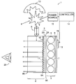
- FIG. 1 shows a schematic representation of a side view through an illuminated nonemissive electronic display according to the present invention.
- FIGS. 2A-2C show schematic representations of a tiled, illuminated, nonemissive electronic display according to embodiments of the invention.
- a single light source is used to illuminate at least one substrate of the tiled display.
- FIG. 2B a plurality of light sources is provided.
- a single light source is provided which is coupled to a plurality of substrates via a plurality of light conduits.
- an illuminated nonemissive electronic display 1 comprises a nonemissive electronic display in combination with an illumination system.
- the nonemissive electronic display includes a substrate 2 having a first surface 2 a and a second surface 2 b .
- a display media 3 is disposed adjacent the first surface 2 a and includes nonemissive display elements 5 having electrically-responsive optical properties.
- the display media 3 is bounded by a front electrode 66 and a back electrode 6 .
- the back electrode 6 is a patterned electrode which selectively alters the optical properties of the display elements 5 in the display media 3 , generating displays of images and/or text, (moving or still) in response to voltages selectively applied to different areas of the display media 3 .
- the illumination system comprises at least one light source 4 which communicates with the display media 3 via a light transmissive element 8 .
- the display media 3 includes nonemissive display elements 5 such as particles, particle-containing capsules (e.g., microencapsulated electrophoretic display elements), bichromal spheres, or rotating round balls, dispersed in a binder 7 .
- the capsules may be of any size or shape.
- the capsules are spherical and have diameters in the millimeter or micron range. In a preferred embodiment, the capsule diameters are from about ten to about a few hundred microns.
- the capsules may be formed by an encapsulation technique and, in one embodiment, include two or more different types of electrophoretically mobile particles.
- Particles contained within the capsules may be colored, luminescent, light-absorbing, light scattering, or transparent, and may come in a variety of shapes (e.g., comer cubes).
- Suitable particle materials include, but are not limited to, neat pigments, dyed (laked) pigments and pigment/polymer composites.
- types of particles include scattering pigments, absorbing pigments and luminescent particles.
- the particles are transparent.
- Exemplary particles comprise titania, which may be coated in one or two layers with a metal oxide, such as aluminum oxide or silicon oxide.
- Exemplary types of luminescent particles comprise zinc sulfide, which may be further encapsulated with an insulative coating to reduce electrical conduction.
- Light-blocking or absorbing particles, such as dyes or pigments are also encompassed within the scope of the invention. Types of dyes for use in electrophoretic displays are commonly known in the art.
- the particles are dispersed in a suspending fluid within the capsules.
- the suspending fluid may be a high resistivity fluid.
- the suspending fluid may be a single fluid, or a mixture of two or more fluids.
- the suspending fluid is a halogenated hydrocarbon, such as tetrachloroethylene.
- the halogenated hydrocarbon may also be a low molecular weight polymer.
- One such low molecular weight polymer is poly(chlorotrifluoroethylene).
- the degree of polymerization for this polymer may be from about 2 to about 10.
- the suspending fluid may comprise a dye to provide colored display elements 5 .
- Useful dyes are typically soluble in the suspending fluid, and may further be part of a polymeric chain. Dyes may be polymerized by thermal, photochemical, and chemical diffusion processes. Single dyes or mixtures of dyes may also be used.
- the suspending fluid comprises a plurality of anisotropic particles and a plurality of second particles.
- Application of a first electric field causes the anisotropic particles to assume a specific orientation and present an optical property.
- Application of a second electric field then causes the plurality of second particles to translate, thereby disorienting the anisotropic particles and disturbing the optical property.
- the orientation of the anisotropic particles may allow easier translation of the plurality of second particles.
- a microencapsulated electrophoretic display using particle-containing capsules can be constructed so that the optical state of the display is stable for some length of time.
- the particles are suspended in a suspending fluid (either a single fluid or a mixture of fluids) whose density is substantially matched to that of the particles.
- a stable display media 3 is generated because the particles will not move in the suspending fluid absent an electric field applied via electrodes 66 and 6 .
- the display When the display has two states that are stable in this manner, the display is bistable. If more than two states of the display are stable, then the display is multistable.
- bistable indicates a display in which any optical state remains fixed once an addressing voltage is removed.
- a slowly decaying optical state can be effectively bistable if the optical state is substantially unchanged over the required viewing time. For example, in a display that is updated every few minutes, a display image that is stable for hours or days is effectively bistable for a particular application.
- the term bistable also indicates a display with an optical state sufficiently long-lived so as to be effectively bistable for a particular application.
- the display media 3 comprises a binder 7 which surrounds display elements 5 and separates the front and back electrodes 66 and 6 .
- Materials for use as binders 7 include, but are not limited to, water-soluble polymers, water-dispersed polymers, oil-soluble polymers, thermoset polymers, thermoplastic polymers, and uv- or radiation-cured polymers.
- the binder 7 material is compatible with the display elements 5 and front and back electrodes 66 and 6 , allowing for facile printing or coating.
- the binder 7 possesses barrier properties for water, oxygen, ultraviolet light, an electrophoretic fluid, or other materials. Further, the binder 7 may contain surfactants and cross-linking agents to improve coating properties and to increase the durability of the display.
- the binder 7 comprises an electrophoretic fluid directly dispersed or emulsified into the binder 7 (or into a precursor to the binder material) to form what may be called a “polymer-dispersed electrophoretic display.”
- the individual electrophoretic phases may be referred to as capsules or microcapsules even though no capsule membrane per se is present.
- Such polymer-dispersed electrophoretic displays are considered to be subsets of encapsulated electrophoretic displays
- an encapsulated electrophoretic display media 3 requires the proper interaction of polymeric binders 7 , capsule membranes, particles, and suspending fluids which must all be chemically compatible.
- the capsule membranes may engage in useful surface interactions with the electrophoretic particles, or may act as an inert physical boundary between the fluid and the binder 7 .
- Polymer binders 7 may set as adhesives between capsule membranes and the electrode surfaces.
- the degree of stability of the display media 3 can be controlled through appropriate chemical modification of the electrophoretic particles, the suspending fluid, the capsule, and binder 7 materials and through the interactions of these components.
- the display media 3 is sandwiched by a front electrode 66 and a back electrode 6 .
- the display elements 5 within the display media 3 change their optical states.
- the back electrode 6 is a patterned electrode which is used to selectively address the display elements 5 within the display media 3 , generating displays of images and/or text (moving or still) in response to voltages selectively applied to different areas of the display media 3 .
- the back electrode 6 is adjacent to the display media 3 .
- the back electrode 6 contacts the display media 3 .
- the back electrode 6 may be disposed on a back electrode substrate 19 , or may be printed onto and part of back electrode substrate 19 .
- the front electrode 66 may be disposed on the first surface 2 a of substrate 2 , or may be printed onto, and part of, substrate 2 .
- the particles may be oriented or translated by placing an electric field across the capsule.
- the electric field may include an alternating-current field or a direct-current field.
- electrodes 66 and 6 can be of relatively high resistivity.
- the ability to use resistive conductors substantially widens the number and types of materials that can be used.
- ITO indium tin oxide
- ITO indium tin oxide
- the replacement of ITO with other materials can provide benefits in appearance, processing capabilities (printed conductors), flexibility, and durability.
- printed electrodes are used, these are in contact only with a solid binder and not with a fluid layer (such as a fluid comprising liquid crystals). This means that some conductive materials, which would otherwise dissolve or be degraded by contact with liquid crystals, can be used.
- Conductive materials used for the front electrode 66 are at least partially transparent and include indium tin oxide or polyaniline. Electroconductive powders (Zelec ECP electroconductive powders, DuPont Chemical Co., Wilmington, Del.) may also be used to create transparent electrodes. Because conductivity requirements are not as stringent, the electrode layers can be made thinner and more transparent than with traditional displays.
- Conductive materials used for back electrode 6 may be either transparent or opaque. Suitable conductive materials for back electrode 6 include opaque metallic inks, such as silver and graphite inks. Organic conductors, such as polymeric conductors and molecular organic conductors may also be used. Suitable materials for polymeric conductors include, but are not limited to, polyaniline and derivatives, polythiophene and derivatives, poly 3,4-ethylenedioxythiophene (PEDOT) and derivatives, polypyrrole and derivatives, and polyphenylenevinylene (PPV) and derivatives. Suitable materials for organic molecular conductors include, but are not limited to, derivatives of naphthalene, pthalocyanine, and pentacene.
- the illuminated nonemissive electronic display 1 comprises at least one light source 4 which communicates with the display media 3 via a light transmissive element 8 .
- Suitable light sources 4 which may used in the present invention include, but are not limited to, cold-cathode fluorescent lamps (CCFL), surface mounting technology (SMT) incandescent lamps, or light emitting diodes (LEDs).
- the light source 4 is side-coupled to the light-transmissive element 8 .
- a light conduit 9 e.g., an optical fiber
- a reflector 10 is provide to direct any light back-reflected from the light transmissive element 8 and/or light conduit 9 back into the light transmissive element 8 and/or light conduit 9 , to the display media 3 , minimizing any loss of light from the light source 4 .
- the reflector 10 comprises a highly light scattering surface which may be patterned (e.g., having sawtoothed ridges, as shown in FIG. 1) to enhance its light scattering effect.
- the light transmissive element 8 comprises a first face 8 a and a second face 8 b .
- the first face 8 a of the light transmissive element 8 is adjacent to the second surface 2 b of the substrate 2 . Illumination from the light source 4 is directed to the display media 3 through the light transmissive element 8 and is refractively distributed evenly through the second face 8 b of the light transmissive element 8 to be received by a viewer 20 .
- the term “adjacent” means in sufficient proximity to the display media 3 for the light transmissive element 8 to illuminate the display media 3 .
- the light transmissive element 8 is in contact with the second surface 2 b of the substrate 2 .
- Light entering the light transmissive element 8 has two fates. While some of the light will exit the light transmissive element 8 through second face 8 b , the remaining light is captured by total internal reflection within the light transmissive element 8 .
- the relationship between the angle of incidence of light falling on the second face 8 b and the angle of refraction (i.e., the angle of the outgoing light) is expressed by Snell's law:
- n 1 is the index of refraction of the light transmissive element 8
- n 2 is the index of refraction of the external media (e.g., air)
- ⁇ 1 is the angle of incidence
- ⁇ 2 is the angle of refraction.
- the angle of refraction, ⁇ 2 is 90°
- sin ⁇ 2 is equal to 1
- the angle of incidence ⁇ 1 is inverse sin of n 2 /n 1 , defining a critical angle ⁇ c , corresponding to the change of the refractive index of the material at both sides of the second surface 8 b .
- Total internal reflection occurs whenever the angle of incidence of ⁇ 1 is greater than the critical angle ⁇ c .
- surface features, or light scattering centers 11 are provided on the first face 8 a of the light transmissive element 8 so that a greater quantity of light falls on second face 8 b with an angle of incidence ⁇ 1 which is less than the critical angle ⁇ c .
- the light scattering centers 11 may assume a variety of shapes including, but not limited to wedge shapes, surfaces with triangular intrusions, ridges, or micro-roughened structures.
- the distribution of light transmissive elements can be modified to provide for the substantially uniform refraction of light along the second face 8 b of the light transmissive element 8 . For example, as shown in FIG.
- an increased number of light scattering elements 8 are provided at the end of the light transmissive element 8 farthest from the light source 4 .
- the thickness and regularity of features, as well as their distribution, may be modified to enhance the uniformity of light transmitted through second face 8 b.
- light directors may be provided to restrict the input of light to angles that will minimize the amount of total internal reflection.
- Light directors encompassed within the scope of the present invention include, but are not limited to, reflectors, refractors, and diffractors.
- the light transmissive element 8 may comprise additional elements to enhance the versatility of the illuminated nonemissive electronic display 1 .
- a light polarizing film 16 is provided adjacent first surface 8 a to increase the uniformity of light passing through the second face 8 b and reaching the viewer 20 .
- a red/green/blue absorptive filter (not shown) is provided adjacent the first face 8 a or second face 8 b of the light transmissive element 8 to alter the wavelength of light passing through the first face 8 a or second face 8 b thereby creating a colored display.
- the light transmissive element 8 is made of a flexible material, e.g., a gelatinous, transparent polymer such as PNMA, polyester, polyethylene, polycarbonate, and acrylic, which is capable of bending with the substrate 2 and display media 3 .
- a gelatinous, transparent polymer such as PNMA, polyester, polyethylene, polycarbonate, and acrylic
- the reflective display 1 can be used to create complex three-dimensional structures which may be selectively illuminated.
- the light transmissive element 8 is a light pipe.
- nonemissive electronic display 1 is selectively illuminated through the use of a photodetector 13 coupled to the light source 4 .
- the photodetector 13 detects the level of ambient light and provides information concerning this level to a controller 14 which is in communication with a power source 15 .
- the power source 15 activates the light source 4 .
- the controller 14 instructs the power source 15 to activate the light source 4 .
- additional sensor elements may be provided, such as a motion detector.
- the controller 14 provides instructions to illuminate the display 1 only when someone passes by the display 1 .
- An audio device may additionally be provided which is coupled to the controller 14 to emit an audio signal in response to a cue from the controller 14 .
- a tiled display 17 which comprises a plurality of substrates 2 c , 2 d , 2 e , and 2 f , each substrate 2 c , 2 d , 2 e , and 2 f having a first surface 2 a and second surface 2 b .
- Display media 3 c , 3 d , 3 e , 3 f each comprising nonemissive display elements 5 (e.g., particles, particle-containing capsules, bichromal spheres and rotating round balls) (not shown), are disposed on the first surface 2 a of each of substrates 2 c , 2 d , 2 e , and 2 f , respectively.
- At least one light source 4 c is in communication with at least one of the substrates 2 c , 2 d , 2 e , and 2 f , via at least one light transmissive element 8 c , 8 d , 8 e , and 8 f , and is capable of illuminating at least one of the display media 3 c , 3 d , 3 e , and 3 f .
- the substrates 2 c , 2 d , 2 e , and 2 f are flexible, allowing the display to assume a three-dimensional shape.
- light transmissive elements 8 c , 8 d , 8 e , and 8 f are also flexible.
- Light source 4 c may be coupled to light transmissive elements 8 c , 8 d , 8 e , and 8 f via light conduit 9 c (e.g., an optical fiber).
- a plurality of light sources 4 c , 4 d , and 4 f may be provided, coupled to a plurality of light transmissive elements 8 c , 8 d , 8 e , and 8 f .
- a light source may be used to illuminate a single substrate or multiple substrates.
- light source 4 c is coupled to a single light transmissive element 8 c via light conduit 9 c and can thereby illuminate substrate 2 c .
- light source 4 f is coupled to light transmissive element 8 f via light conduit 9 f and can thereby illuminate substrate 2 f .
- light source 4 d illuminates two substrates, 2 d and 2 e , by being side-coupled to two light transmissive elements 8 d and 8 e via a single light conduit 9 d.
- At least one light source, 4 c , 4 d , or 4 e is in communication with at least one photodetector 13 via controller 14 and power source 15 .
- individual substrates 2 c , 2 d , 2 e , and 2 f and display media 3 c , 3 d , 3 e , and 3 f of the tiled display 17 are selectively illuminated in response to signals from the controller 14 which instruct power source 15 to activate any, or all of, light source(s) 4 c , 4 d , and 4 f , when light drops below a selected value.
- FIG. 1 in the embodiment of the invention shown in FIG.
- a curved tiled display 17 which is by a window 18 comprises at least one photodetector 13 on each substrate 2 c , 2 d , 2 e , and 2 f .
- the substrate which is farthest from the window 18 i.e., substrate 2 f
- the substrate which is farthest from the window 18 is illuminated first as light detected by the photodetector 13 on substrate 2 f falls below the selected value, causing light source 4 f to be activated.
- light sources 4 b and 4 a become activated, illuminating adjacent substrates 2 e , 2 d , and 2 c.
- a single light source 4 c may be provided coupled to a plurality of light transmissive elements 8 c , 8 d , 8 e , and 8 f by means of connecting light conduits 9 c , 9 d , and 9 e (e.g., arrays of optical fibers).
- the tiled display 17 provides a means to form a multicharacter display in a variety of three-dimensional shapes, including, but not limited to cylinders, waves, cubes, and curved sections.
- a static display can be used to create the impression of motion.
- images may be made to appear to move in response to viewer's behavior.
- Changes in the optical properties of multiple substrates 2 may be coordinated, for example using a plurality of transducers (not shown), each transducer in electrical communication with a different substrate 2 .
- Transducers may be connected to each other to create a multi-level transducer path which changes the state of the tiled display 17 .
- the plurality of substrates can create a large area, multicharacter display. By seamlessly positioning individual substrates 2 , the distinctions between individual substrates 2 can be made to disappear, creating the effect of a single large area display substrate 2 .
- a tiled display system 17 may include substrates 2 having a plurality of pixels, each pixel having its own lead line to controller 14 .
- Each lead line may be a discrete or packaged transistor line.
- one surface of the substrate 2 comprises a grid of electrodes, 6 , each electrode connected through a via to the output of a control chip.
- N2+1 control lines are needed.
- An additional line is used to connect the control lines to the electrode 6 .
- a matrix display using 2N+1 control lines can be built with a plurality of tiled displays 17 using a variety of techniques.
- an array of varistors, metal-insulator-metal, or discrete diodes are used for individually addressing each pixel. In the case of diodes, discrete surface-mount zener diodes are useful.
- the substrates 2 /display media 3 /light emissive elements 8 are connected to each other using cables.
- the substrates 2 /display media 3 /light transmissive elements 8 can be mounted to a wall, lightweight metal grid, or any other surface, using nuts soldered onto the back of the substrates 2 , or by any other means known in the art of fastening substrates 2 .
- a frame may be provided to enclose the display, and standard wall fasteners may be attached to the back of the frame.
- the controller 14 includes a microprocessor or other suitable drive circuitry.
- the controller 14 transmits information to the tile displays 17 to update the display using any convenient form of electromagnetic radiation.
- the controller 14 also receives information from the display (e.g., from photodetector 13 , motion sensors, and other sensors disposed on substrates 2 ).
- Data for the tiled display 17 may be stored in a memory element of the controller 14 or may be received in the form of electromagnetic signals using a receiver (not shown).
- the receiver for example, can include an antenna and a passive rectifier in communication with the antenna, as described above.
- the power source 15 connects to a single substrate (e.g., 2 c , 2 d , 2 e , or 2 f ) and controls the entire display 17 .
- the power source 15 can consist of a battery, a power supply, a paging receiver, and a microprocessor to control the entire system.
- the tiled display 17 can be powered using commercially available integrated AC to DC converters.
- each substrate 2 may have its own power source 15 (e.g., a high voltage supply). Common inverter chips may be used in this embodiment.
- One method of controlling the entire tiled display 17 is to have a separate controller 14 positioned on each substrate 2 .
- the controller 14 tells one substrate 2 to which it is connected that it is at a certain coordinate location, e.g., 0,0. Due to the asymmetrical connector layout, the substrate 2 can determine to which edge the controller 14 is connected. That individual substrate 2 then communicates with its neighbors, increasing or decreasing the coordinate location appropriately. Through this protocol, each substrate 2 can determine a unique identification code that specifies its location on the tiled display 17 . The controller 14 can then send data out on a common bus, and each substrate 2 's controller 14 can receive data needed to update the display on the substrate 2 .
- the controller 14 shifts this data out to display drivers (not shown).
- the entire tiled display 17 is given a write pulse and the entire tiled display 17 is updated.
- the tiled display 17 described above may be successfully driven with a voltage as low as 3 volts.
- high voltage CMOS display drive circuitry such as HV57708PG manufactured by Supertex Corporation (Sunnyvale, Calif.) can be used to drive the tiled display 17 .
- HV57708PG is an 80 pin plastic gull wing surface mount chip that has 64 outputs. Each output can sink 15 mA. Four of these chips can control a single substrate 2 .
- Other chips may find utility in the context of the present invention, such as the Sharp LH1538 which is an 80V 128 line Tape-Automated-Bonded (TAB) chip.
- TAB Tape-Automated-Bonded
- Electrophoretic displays have been the subject of intense research and development for a number of years. Electrophoretic displays have attributes of good brightness and contrast, wide viewing angles, state bistability, and low power consumption when compared with other nonemissive displays. Encapsulated electrophoretic displays typically do not suffer from the clustering and settling failure mode of traditional electrophoretic devices and provides further advantages, such as the ability to print or coat the display media 3 on a wide variety of flexible and rigid substrates 2 .
- printing is intended to include all forms of printing and coating, including, but without limitation: premetered coatings such as patch die coating, slot or extrusion coating, slide or cascade coating, and curtain coating; roll coating such as knife over roll coating, forward and reverse roll coating; gravure coating; dip coating; spray coating; meniscus coating; spin coating; brush coating; air knife coating; silk screen printing processes; electrostatic printing processes; thermal printing processes; and other similar techniques.
- premetered coatings such as patch die coating, slot or extrusion coating, slide or cascade coating, and curtain coating
- roll coating such as knife over roll coating, forward and reverse roll coating
- gravure coating dip coating
- spray coating meniscus coating
- spin coating spin coating
- brush coating air knife coating
- silk screen printing processes electrostatic printing processes
- thermal printing processes thermal printing processes; and other similar techniques.
- microencapsulated electrophoretic displays are used to create multicharacter displays that can be conformed to a variety of shapes. Such displays are long-lived, consume little power, and maintain their effectiveness through the use of selective illumination provided by the illumination system.
Abstract
Description
Claims (17)
Priority Applications (1)
| Application Number | Priority Date | Filing Date | Title |
|---|---|---|---|
| US09/413,934 US6376828B1 (en) | 1998-10-07 | 1999-10-07 | Illumination system for nonemissive electronic displays |
Applications Claiming Priority (2)
| Application Number | Priority Date | Filing Date | Title |
|---|---|---|---|
| US10338498P | 1998-10-07 | 1998-10-07 | |
| US09/413,934 US6376828B1 (en) | 1998-10-07 | 1999-10-07 | Illumination system for nonemissive electronic displays |
Publications (1)
| Publication Number | Publication Date |
|---|---|
| US6376828B1 true US6376828B1 (en) | 2002-04-23 |
Family
ID=22294904
Family Applications (1)
| Application Number | Title | Priority Date | Filing Date |
|---|---|---|---|
| US09/413,934 Expired - Lifetime US6376828B1 (en) | 1998-10-07 | 1999-10-07 | Illumination system for nonemissive electronic displays |
Country Status (8)
| Country | Link |
|---|---|
| US (1) | US6376828B1 (en) |
| EP (1) | EP1118039B1 (en) |
| JP (2) | JP4679726B2 (en) |
| AT (1) | ATE232307T1 (en) |
| AU (1) | AU6295899A (en) |
| CA (1) | CA2346167C (en) |
| DE (1) | DE69905266T2 (en) |
| WO (1) | WO2000020923A1 (en) |
Cited By (197)
| Publication number | Priority date | Publication date | Assignee | Title |
|---|---|---|---|---|
| US20020050976A1 (en) * | 2000-11-02 | 2002-05-02 | Fuji Xerox Co., Ltd. | Image display medium, Image display device, and image display method |
| US20020090980A1 (en) * | 2000-12-05 | 2002-07-11 | Wilcox Russell J. | Displays for portable electronic apparatus |
| US20020130832A1 (en) * | 2001-03-13 | 2002-09-19 | Baucom Allan Scott | Apparatus for displaying drawings |
| US20020131147A1 (en) * | 1998-08-27 | 2002-09-19 | Paolini Richard J. | Electrophoretic medium and process for the production thereof |
| US20020154382A1 (en) * | 2001-04-19 | 2002-10-24 | Morrison Ian D. | Electrochromic-nanoparticle displays |
| US20020171910A1 (en) * | 2001-05-15 | 2002-11-21 | Pullen Anthony Edward | Electrophoretic displays containing magnetic particles |
| US20020180687A1 (en) * | 2001-04-02 | 2002-12-05 | E Ink Corporation | Electrophoretic medium and display with improved image stability |
| US20020190936A1 (en) * | 1999-09-28 | 2002-12-19 | Brother International Corporation | Methods and apparatus for subjecting an element to an electrical filed |
| US20030011560A1 (en) * | 1998-08-27 | 2003-01-16 | E Ink Corporation | Electrophoretic display comprising optical biasing element |
| US20030011867A1 (en) * | 2001-07-09 | 2003-01-16 | Loxley Andrew L. | Electro-optic display and adhesive composition for use therein |
| US20030025855A1 (en) * | 2001-07-09 | 2003-02-06 | E Lnk Corporation | Electro-optic display and lamination adhesive |
| US20030038755A1 (en) * | 2001-08-16 | 2003-02-27 | E Ink Corporation | Light modulation by frustration of total internal reflection |
| US20030053189A1 (en) * | 2001-09-14 | 2003-03-20 | E Ink Corporation | Methods for addressing electro-optic materials |
| US20030137521A1 (en) * | 1999-04-30 | 2003-07-24 | E Ink Corporation | Methods for driving bistable electro-optic displays, and apparatus for use therein |
| US20030214695A1 (en) * | 2002-03-18 | 2003-11-20 | E Ink Corporation | Electro-optic displays, and methods for driving same |
| US20030222315A1 (en) * | 2002-04-24 | 2003-12-04 | E Ink Corporation | Backplanes for display applications, and components for use therein |
| WO2003107315A2 (en) | 2002-06-13 | 2003-12-24 | E Ink Corporation | Methods for driving electro-optic displays |
| US20040014265A1 (en) * | 2002-04-24 | 2004-01-22 | E Ink Corporation | Processes for forming backplanes for electro-optic displays |
| US20040012839A1 (en) * | 2002-05-23 | 2004-01-22 | E Ink Corporation | Capsules, materials for use therein and electrophoretic media and displays containing such capsules |
| US20040027327A1 (en) * | 2002-06-10 | 2004-02-12 | E Ink Corporation | Components and methods for use in electro-optic displays |
| US6704133B2 (en) | 1998-03-18 | 2004-03-09 | E-Ink Corporation | Electro-optic display overlays and systems for addressing such displays |
| US6724374B1 (en) * | 1999-10-25 | 2004-04-20 | Silverbrook Research Pty Ltd | Sensing device for coded electronic ink surface |
| US20040105036A1 (en) * | 2002-08-06 | 2004-06-03 | E Ink Corporation | Protection of electro-optic displays against thermal effects |
| US20040112750A1 (en) * | 2002-09-03 | 2004-06-17 | E Ink Corporation | Electrophoretic medium with gaseous suspending fluid |
| US20040136048A1 (en) * | 1995-07-20 | 2004-07-15 | E Ink Corporation | Dielectrophoretic displays |
| US20040155857A1 (en) * | 2002-09-03 | 2004-08-12 | E Ink Corporation | Electro-optic displays |
| US20040196215A1 (en) * | 2002-12-16 | 2004-10-07 | E Ink Corporation | Backplanes for electro-optic displays |
| US6816147B2 (en) | 2000-08-17 | 2004-11-09 | E Ink Corporation | Bistable electro-optic display, and method for addressing same |
| US20040226820A1 (en) * | 2003-03-25 | 2004-11-18 | E Ink Corporation | Processes for the production of electrophoretic displays |
| US6822782B2 (en) | 2001-05-15 | 2004-11-23 | E Ink Corporation | Electrophoretic particles and processes for the production thereof |
| US20040233509A1 (en) * | 2002-12-23 | 2004-11-25 | E Ink Corporation | Flexible electro-optic displays |
| US20040252360A1 (en) * | 2001-07-09 | 2004-12-16 | E Ink Corporation | Electro-optic display and lamination adhesive for use therein |
| US20040257635A1 (en) * | 2003-01-31 | 2004-12-23 | E Ink Corporation | Construction of electrophoretic displays |
| US20050001812A1 (en) * | 1999-04-30 | 2005-01-06 | E Ink Corporation | Methods for driving bistable electro-optic displays, and apparatus for use therein |
| US6842279B2 (en) | 2002-06-27 | 2005-01-11 | E Ink Corporation | Illumination system for nonemissive electronic displays |
| US20050007653A1 (en) * | 2003-03-27 | 2005-01-13 | E Ink Corporation | Electro-optic assemblies, and materials for use therein |
| US20050012980A1 (en) * | 2003-05-02 | 2005-01-20 | E Ink Corporation | Electrophoretic displays with controlled amounts of pigment |
| US20050024353A1 (en) * | 2001-11-20 | 2005-02-03 | E Ink Corporation | Methods for driving electro-optic displays |
| US20050041004A1 (en) * | 2003-08-19 | 2005-02-24 | E Ink Corporation | Method for controlling electro-optic display |
| US20050062714A1 (en) * | 2003-09-19 | 2005-03-24 | E Ink Corporation | Methods for reducing edge effects in electro-optic displays |
| US20050067656A1 (en) * | 2000-04-18 | 2005-03-31 | E Ink Corporation | Process for fabricating thin film transistors |
| US20050078099A1 (en) * | 2002-04-24 | 2005-04-14 | E Ink Corporation | Electro-optic displays, and components for use therein |
| US20050105162A1 (en) * | 2001-03-19 | 2005-05-19 | Paolini Richard J.Jr. | Electrophoretic medium and process for the production thereof |
| US20050122565A1 (en) * | 2003-11-05 | 2005-06-09 | E Ink Corporation | Electro-optic displays, and materials for use therein |
| US20050122564A1 (en) * | 1999-05-03 | 2005-06-09 | E Ink Corporation | Machine-readable displays |
| US20050122284A1 (en) * | 2003-11-25 | 2005-06-09 | E Ink Corporation | Electro-optic displays, and methods for driving same |
| US20050134554A1 (en) * | 2001-07-27 | 2005-06-23 | E Ink Corporation | Microencapsulated electrophoretic display with integrated driver |
| US20050151709A1 (en) * | 2003-10-08 | 2005-07-14 | E Ink Corporation | Electro-wetting displays |
| US20050152022A1 (en) * | 2003-12-31 | 2005-07-14 | E Ink Corporation | Electro-optic displays, and method for driving same |
| US20050168801A1 (en) * | 2004-01-16 | 2005-08-04 | E Ink Corporation | Process for sealing electro-optic displays |
| US20050179642A1 (en) * | 2001-11-20 | 2005-08-18 | E Ink Corporation | Electro-optic displays with reduced remnant voltage |
| US20050190137A1 (en) * | 2004-02-27 | 2005-09-01 | E Ink Corporation | Backplanes for electro-optic displays |
| US20050195469A1 (en) * | 2004-03-02 | 2005-09-08 | Van Brocklin Andrew L. | Phase change electrophoretic imaging for rewritable applications |
| US20050212747A1 (en) * | 2004-03-26 | 2005-09-29 | E Ink Corporation | Methods for driving bistable electro-optic displays |
| US20050213191A1 (en) * | 2004-03-23 | 2005-09-29 | E Ink Corporation | Light modulators |
| US20050253777A1 (en) * | 2004-05-12 | 2005-11-17 | E Ink Corporation | Tiled displays and methods for driving same |
| US20050270261A1 (en) * | 1999-04-30 | 2005-12-08 | Danner Guy M | Methods for driving electro-optic displays, and apparatus for use therein |
| US20050280626A1 (en) * | 2001-11-20 | 2005-12-22 | E Ink Corporation | Methods and apparatus for driving electro-optic displays |
| US20060023296A1 (en) * | 2004-07-27 | 2006-02-02 | E Ink Corporation | Electro-optic displays |
| US20060118901A1 (en) * | 2004-11-17 | 2006-06-08 | Plextronics, Inc. | Heteroatomic regioregular poly(3-substitutedthiophenes) as thin film conductors in diodes whcih are not light emitting or photovoltaic |
| US20060139308A1 (en) * | 1995-07-20 | 2006-06-29 | E Ink Corporation | Addressing schemes for electronic displays |
| US20060176267A1 (en) * | 2003-07-24 | 2006-08-10 | E Ink Corporation | Improvements in electro-optic displays |
| US7110164B2 (en) | 2002-06-10 | 2006-09-19 | E Ink Corporation | Electro-optic displays, and processes for the production thereof |
| US20060209388A1 (en) * | 2005-01-26 | 2006-09-21 | E Ink Corporation | Electrophoretic displays using gaseous fluids |
| US20060279527A1 (en) * | 1999-05-03 | 2006-12-14 | E Ink Corporation | Machine-readable displays |
| US20070035808A1 (en) * | 2001-07-09 | 2007-02-15 | E Ink Corporation | Electro-optic display and materials for use therein |
| US20070085818A1 (en) * | 1999-07-21 | 2007-04-19 | E Ink Corporation | Use of a storage capacitor to enhance the performance of an active matrix driven electronic display |
| US20070091417A1 (en) * | 2005-10-25 | 2007-04-26 | E Ink Corporation | Electrophoretic media and displays with improved binder |
| WO2007104003A2 (en) | 2006-03-08 | 2007-09-13 | E Ink Corporation | Methods for production of electro-optic displays |
| US20070223079A1 (en) * | 2006-03-22 | 2007-09-27 | E Ink Corporation | Electro-optic media produced using ink jet printing |
| US20070247697A1 (en) * | 2003-11-05 | 2007-10-25 | E Ink Corporation | Electro-optic displays, and materials for use therein |
| US20070286975A1 (en) * | 2003-11-05 | 2007-12-13 | E Ink Corporation | Electro-optic displays, and materials for use therein |
| US20080013156A1 (en) * | 2006-07-13 | 2008-01-17 | E Ink Corporation | Particles for use in electrophoretic displays |
| US20080013155A1 (en) * | 2006-07-11 | 2008-01-17 | E Ink Corporation | Electrophoretic medium and display with improved image stability |
| US20080024429A1 (en) * | 2006-07-25 | 2008-01-31 | E Ink Corporation | Electrophoretic displays using gaseous fluids |
| US20080024482A1 (en) * | 2002-06-13 | 2008-01-31 | E Ink Corporation | Methods for driving electro-optic displays |
| US20080023332A1 (en) * | 2003-03-25 | 2008-01-31 | E Ink Corporation | Processes for the production of electrophoretic displays |
| US20080030832A1 (en) * | 2006-08-02 | 2008-02-07 | E Ink Corporation | Multi-layer light modulator |
| US20080043318A1 (en) * | 2005-10-18 | 2008-02-21 | E Ink Corporation | Color electro-optic displays, and processes for the production thereof |
| US20080048969A1 (en) * | 2003-06-30 | 2008-02-28 | E Ink Corporation | Methods for driving electrophoretic displays |
| US20080057252A1 (en) * | 2002-06-10 | 2008-03-06 | E Ink Corporation | Components and methods for use in electro-optic displays |
| US20080074730A1 (en) * | 2006-09-22 | 2008-03-27 | E Ink Corporation | Electro-optic display and materials for use therein |
| US20080117495A1 (en) * | 1995-07-20 | 2008-05-22 | E Ink Corporation | Dielectrophoretic displays |
| US20080129667A1 (en) * | 2004-03-31 | 2008-06-05 | E Ink Corporation | Methods for driving electro-optic displays |
| US20080137176A1 (en) * | 2006-12-07 | 2008-06-12 | E Ink Corporation | Components and methods for use in electro-optic displays |
| US20080165121A1 (en) * | 2007-01-09 | 2008-07-10 | Samsung Sdi Co., Ltd. | Electrophoretic display apparatus and manufacturing method thereof |
| US20080174853A1 (en) * | 2007-01-22 | 2008-07-24 | E Ink Corporation | Multi-layer sheet for use in electro-optic displays |
| US7411719B2 (en) | 1995-07-20 | 2008-08-12 | E Ink Corporation | Electrophoretic medium and process for the production thereof |
| US20080218839A1 (en) * | 2003-11-05 | 2008-09-11 | E Ink Corporation | Electro-optic displays, and materials for use therein |
| US20080259432A1 (en) * | 2007-04-17 | 2008-10-23 | Seiko Epson Corporation | Electrophoresis display device and electronic apparatus |
| US20080266646A1 (en) * | 1995-07-20 | 2008-10-30 | E Ink Corporation | Electrophoretic displays with controlled amounts of pigment |
| US20080266245A1 (en) * | 2001-04-02 | 2008-10-30 | E Ink Corporation | Electrophoretic displays with controlled amounts of pigment |
| US7453445B2 (en) | 2004-08-13 | 2008-11-18 | E Ink Corproation | Methods for driving electro-optic displays |
| US20080291129A1 (en) * | 2007-05-21 | 2008-11-27 | E Ink Corporation | Methods for driving video electro-optic displays |
| US20080309350A1 (en) * | 2006-03-08 | 2008-12-18 | E Ink Corporation | Electro-optic displays, and materials and methods for production thereof |
| US20080316582A1 (en) * | 2006-03-08 | 2008-12-25 | E Ink Corporation | Electro-optic displays, and materials and methods for production thereof |
| US20090004442A1 (en) * | 2007-06-28 | 2009-01-01 | E Ink Corporation | Processes for the production of electro-optic displays, and color filters for use therein |
| US20090000729A1 (en) * | 2007-06-29 | 2009-01-01 | E Ink Corporation | Electro-optic displays, and materials and methods for production thereof |
| US20090109519A1 (en) * | 2007-03-06 | 2009-04-30 | E Ink Corporation | Materials for use in electrophoretic displays |
| US20090122389A1 (en) * | 2007-11-14 | 2009-05-14 | E Ink Corporation | Electro-optic assemblies, and adhesives and binders for use therein |
| US7554712B2 (en) | 2005-06-23 | 2009-06-30 | E Ink Corporation | Edge seals for, and processes for assembly of, electro-optic displays |
| US20090237776A1 (en) * | 2008-03-21 | 2009-09-24 | E Ink Corporation | Electro-optic displays, and color filters for use therein |
| US7649674B2 (en) | 2002-06-10 | 2010-01-19 | E Ink Corporation | Electro-optic display with edge seal |
| US7679814B2 (en) | 2001-04-02 | 2010-03-16 | E Ink Corporation | Materials for use in electrophoretic displays |
| US7688497B2 (en) | 2007-01-22 | 2010-03-30 | E Ink Corporation | Multi-layer sheet for use in electro-optic displays |
| US20100165446A1 (en) * | 2002-06-10 | 2010-07-01 | E Ink Corporation | Components and methods for use in electro-optic displays |
| US20100201646A1 (en) * | 2006-03-31 | 2010-08-12 | Sony Corporation, A Japanese Corporation | E-ink touchscreen visualizer for home av system |
| US20100225995A1 (en) * | 2009-03-03 | 2010-09-09 | E Ink Corporation | Electro-optic displays, and color filters for use therein |
| US20100289736A1 (en) * | 2009-02-09 | 2010-11-18 | E Ink Corporation | Electrophoretic particles, and processes for the production thereof |
| US7839564B2 (en) | 2002-09-03 | 2010-11-23 | E Ink Corporation | Components and methods for use in electro-optic displays |
| US7843621B2 (en) | 2002-06-10 | 2010-11-30 | E Ink Corporation | Components and testing methods for use in the production of electro-optic displays |
| US7893435B2 (en) | 2000-04-18 | 2011-02-22 | E Ink Corporation | Flexible electronic circuits and displays including a backplane comprising a patterned metal foil having a plurality of apertures extending therethrough |
| US20110164307A1 (en) * | 2002-06-10 | 2011-07-07 | E Ink Corporation | Electro-optic displays, and processes for the production thereof |
| US7986450B2 (en) | 2006-09-22 | 2011-07-26 | E Ink Corporation | Electro-optic display and materials for use therein |
| US7999787B2 (en) | 1995-07-20 | 2011-08-16 | E Ink Corporation | Methods for driving electrophoretic displays using dielectrophoretic forces |
| US8040594B2 (en) | 1997-08-28 | 2011-10-18 | E Ink Corporation | Multi-color electrophoretic displays |
| US8115729B2 (en) | 1999-05-03 | 2012-02-14 | E Ink Corporation | Electrophoretic display element with filler particles |
| US8125501B2 (en) | 2001-11-20 | 2012-02-28 | E Ink Corporation | Voltage modulated driver circuits for electro-optic displays |
| US8314784B2 (en) | 2008-04-11 | 2012-11-20 | E Ink Corporation | Methods for driving electro-optic displays |
| US8319759B2 (en) | 2003-10-08 | 2012-11-27 | E Ink Corporation | Electrowetting displays |
| EP2555182A1 (en) | 2007-02-02 | 2013-02-06 | E Ink Corporation | Electrophoretic displays having transparent electrode and conductor connected thereto |
| US8446664B2 (en) | 2010-04-02 | 2013-05-21 | E Ink Corporation | Electrophoretic media, and materials for use therein |
| WO2013074167A1 (en) | 2011-11-18 | 2013-05-23 | Avon Products, Inc. | Use of electrophoretic microcapsules in a cosmetic composition |
| US8466852B2 (en) | 1998-04-10 | 2013-06-18 | E Ink Corporation | Full color reflective display with multichromatic sub-pixels |
| US8593396B2 (en) | 2001-11-20 | 2013-11-26 | E Ink Corporation | Methods and apparatus for driving electro-optic displays |
| US8610988B2 (en) | 2006-03-09 | 2013-12-17 | E Ink Corporation | Electro-optic display with edge seal |
| US20130334972A1 (en) * | 2011-03-08 | 2013-12-19 | Dolby Laboratories Licensinc Corporation | Illuminator for reflective displays |
| US20140016321A1 (en) * | 2012-07-10 | 2014-01-16 | E Ink Holdings Inc. | Lamp |
| US8654436B1 (en) | 2009-10-30 | 2014-02-18 | E Ink Corporation | Particles for use in electrophoretic displays |
| EP2711770A2 (en) | 2005-10-18 | 2014-03-26 | E Ink Corporation | Components for electro-optic displays |
| US8754859B2 (en) | 2009-10-28 | 2014-06-17 | E Ink Corporation | Electro-optic displays with touch sensors and/or tactile feedback |
| US8902153B2 (en) | 2007-08-03 | 2014-12-02 | E Ink Corporation | Electro-optic displays, and processes for their production |
| US9005494B2 (en) | 2004-01-20 | 2015-04-14 | E Ink Corporation | Preparation of capsules |
| EP2916312A1 (en) | 2001-11-20 | 2015-09-09 | E Ink Corporation | Methods for driving bistable electro-optic displays |
| US20150294363A1 (en) * | 2014-04-10 | 2015-10-15 | Bumper Glass LLC | Prioritized location based ad display |
| EP2947647A2 (en) | 2003-06-30 | 2015-11-25 | E Ink Corporation | Methods for driving electro-optic displays |
| US9280029B2 (en) | 2013-05-13 | 2016-03-08 | Clearink Displays, Inc. | Registered reflective element for a brightness enhanced TIR display |
| US9293511B2 (en) | 1998-07-08 | 2016-03-22 | E Ink Corporation | Methods for achieving improved color in microencapsulated electrophoretic devices |
| US20160147216A1 (en) * | 2010-12-17 | 2016-05-26 | Deckel Maho Pfronten Gmbh | Apparatus for monitoring and providing visual representations of the operating conditions of machine tool parameters |
| US9412314B2 (en) | 2001-11-20 | 2016-08-09 | E Ink Corporation | Methods for driving electro-optic displays |
| US9470950B2 (en) | 2002-06-10 | 2016-10-18 | E Ink Corporation | Electro-optic displays, and processes for the production thereof |
| WO2016191673A1 (en) | 2015-05-27 | 2016-12-01 | E Ink Corporation | Methods and circuitry for driving display devices |
| US9530363B2 (en) | 2001-11-20 | 2016-12-27 | E Ink Corporation | Methods and apparatus for driving electro-optic displays |
| US9529240B2 (en) | 2014-01-17 | 2016-12-27 | E Ink Corporation | Controlled polymeric material conductivity for use in a two-phase electrode layer |
| US9612501B2 (en) | 2013-09-30 | 2017-04-04 | Clearink Displays, Inc. | Method and apparatus for front-lit semi-retro-reflective display |
| US9620067B2 (en) | 2003-03-31 | 2017-04-11 | E Ink Corporation | Methods for driving electro-optic displays |
| US9664978B2 (en) | 2002-10-16 | 2017-05-30 | E Ink Corporation | Electrophoretic displays |
| US9671635B2 (en) | 2014-02-07 | 2017-06-06 | E Ink Corporation | Electro-optic display backplane structures with drive components and pixel electrodes on opposed surfaces |
| US9684163B2 (en) | 2010-12-03 | 2017-06-20 | E Ink Corporation | Methods, systems, and products for illuminating displays |
| US9715155B1 (en) | 2013-01-10 | 2017-07-25 | E Ink Corporation | Electrode structures for electro-optic displays |
| US9726957B2 (en) | 2013-01-10 | 2017-08-08 | E Ink Corporation | Electro-optic display with controlled electrochemical reactions |
| US9740075B2 (en) | 2013-09-10 | 2017-08-22 | Clearink Displays, Inc. | Method and system for perforated reflective film display device |
| US9835925B1 (en) | 2015-01-08 | 2017-12-05 | E Ink Corporation | Electro-optic displays, and processes for the production thereof |
| US9891370B2 (en) | 2011-11-17 | 2018-02-13 | At&T Intellectual Property I, L.P. | Methods, systems, and products for image displays |
| US9897890B2 (en) | 2014-10-07 | 2018-02-20 | Clearink Displays, Inc. | Reflective image display with threshold |
| US9939706B2 (en) | 2013-03-26 | 2018-04-10 | Clearink Displays, Inc. | Displaced porous electrode for frustrating TIR and returning light through exit pupil |
| US9939707B2 (en) | 2013-07-08 | 2018-04-10 | Clearink Displays, Inc. | TIR-modulated wide viewing angle display |
| US10048563B2 (en) | 2003-11-05 | 2018-08-14 | E Ink Corporation | Electro-optic displays, and materials for use therein |
| US10175550B2 (en) | 2014-11-07 | 2019-01-08 | E Ink Corporation | Applications of electro-optic displays |
| US10190743B2 (en) | 2012-04-20 | 2019-01-29 | E Ink Corporation | Illumination systems for reflective displays |
| US10203436B2 (en) | 2013-05-22 | 2019-02-12 | Clearink Displays, Inc. | Method and apparatus for improved color filter saturation |
| US10261221B2 (en) | 2015-12-06 | 2019-04-16 | Clearink Displays, Inc. | Corner reflector reflective image display |
| WO2019089042A1 (en) | 2017-11-03 | 2019-05-09 | E Ink Corporation | Processes for producing electro-optic displays |
| US10304394B2 (en) | 2014-10-08 | 2019-05-28 | Clearink Displays, Inc. | Color filter registered reflective display |
| US10317767B2 (en) | 2014-02-07 | 2019-06-11 | E Ink Corporation | Electro-optic display backplane structure with drive components and pixel electrodes on opposed surfaces |
| US10324577B2 (en) | 2017-02-28 | 2019-06-18 | E Ink Corporation | Writeable electrophoretic displays including sensing circuits and styli configured to interact with sensing circuits |
| US10386547B2 (en) | 2015-12-06 | 2019-08-20 | Clearink Displays, Inc. | Textured high refractive index surface for reflective image displays |
| US10386691B2 (en) | 2015-06-24 | 2019-08-20 | CLEARink Display, Inc. | Method and apparatus for a dry particle totally internally reflective image display |
| US10446585B2 (en) | 2014-03-17 | 2019-10-15 | E Ink Corporation | Multi-layer expanding electrode structures for backplane assemblies |
| US10466565B2 (en) | 2017-03-28 | 2019-11-05 | E Ink Corporation | Porous backplane for electro-optic display |
| US10475396B2 (en) | 2015-02-04 | 2019-11-12 | E Ink Corporation | Electro-optic displays with reduced remnant voltage, and related apparatus and methods |
| US10495941B2 (en) | 2017-05-19 | 2019-12-03 | E Ink Corporation | Foldable electro-optic display including digitization and touch sensing |
| US10527899B2 (en) | 2016-05-31 | 2020-01-07 | E Ink Corporation | Backplanes for electro-optic displays |
| US10573257B2 (en) | 2017-05-30 | 2020-02-25 | E Ink Corporation | Electro-optic displays |
| WO2020060960A1 (en) | 2018-09-17 | 2020-03-26 | E Ink Corporation | Backplanes with hexagonal and triangular electrodes |
| WO2020097462A1 (en) | 2018-11-09 | 2020-05-14 | E Ink Corporation | Electro-optic displays |
| WO2020122917A1 (en) | 2018-12-13 | 2020-06-18 | E Ink Corporation | Illumination systems for reflective displays |
| US10705404B2 (en) | 2013-07-08 | 2020-07-07 | Concord (Hk) International Education Limited | TIR-modulated wide viewing angle display |
| US10726798B2 (en) | 2003-03-31 | 2020-07-28 | E Ink Corporation | Methods for operating electro-optic displays |
| US10824042B1 (en) | 2017-10-27 | 2020-11-03 | E Ink Corporation | Electro-optic display and composite materials having low thermal sensitivity for use therein |
| US10882042B2 (en) | 2017-10-18 | 2021-01-05 | E Ink Corporation | Digital microfluidic devices including dual substrates with thin-film transistors and capacitive sensing |
| US11081066B2 (en) | 2018-02-15 | 2021-08-03 | E Ink Corporation | Via placement for slim border electro-optic display backplanes with decreased capacitive coupling between t-wires and pixel electrodes |
| US11175561B1 (en) | 2018-04-12 | 2021-11-16 | E Ink Corporation | Electrophoretic display media with network electrodes and methods of making and using the same |
| US11250794B2 (en) | 2004-07-27 | 2022-02-15 | E Ink Corporation | Methods for driving electrophoretic displays using dielectrophoretic forces |
| US11397361B2 (en) | 2015-06-29 | 2022-07-26 | E Ink Corporation | Method for mechanical and electrical connection to display electrodes |
| US11404013B2 (en) | 2017-05-30 | 2022-08-02 | E Ink Corporation | Electro-optic displays with resistors for discharging remnant charges |
| US11467466B2 (en) | 2012-04-20 | 2022-10-11 | E Ink Corporation | Illumination systems for reflective displays |
| US11513415B2 (en) | 2020-06-03 | 2022-11-29 | E Ink Corporation | Foldable electrophoretic display module including non-conductive support plate |
| US11511096B2 (en) | 2018-10-15 | 2022-11-29 | E Ink Corporation | Digital microfluidic delivery device |
| US11521565B2 (en) | 2018-12-28 | 2022-12-06 | E Ink Corporation | Crosstalk reduction for electro-optic displays |
| US11537024B2 (en) | 2018-12-30 | 2022-12-27 | E Ink California, Llc | Electro-optic displays |
| US11733580B2 (en) | 2010-05-21 | 2023-08-22 | E Ink Corporation | Method for driving two layer variable transmission display |
| WO2023164078A1 (en) | 2022-02-25 | 2023-08-31 | E Ink Corporation | Electro-optic displays with edge seal components and methods of making the same |
| WO2023167901A1 (en) | 2022-03-01 | 2023-09-07 | E Ink California, Llc | Temperature compensation in electro-optic displays |
| WO2023211699A1 (en) | 2022-04-27 | 2023-11-02 | E Ink Corporation | Electro-optic display stacks with segmented electrodes and methods of making the same |
| US11892739B2 (en) | 2020-02-07 | 2024-02-06 | E Ink Corporation | Electrophoretic display layer with thin film top electrode |
| US11935495B2 (en) | 2021-08-18 | 2024-03-19 | E Ink Corporation | Methods for driving electro-optic displays |
Families Citing this family (6)
| Publication number | Priority date | Publication date | Assignee | Title |
|---|---|---|---|---|
| WO2002021042A1 (en) * | 2000-09-11 | 2002-03-14 | Koninklijke Philips Electronics N.V. | Display device |
| US7261647B2 (en) | 2005-02-18 | 2007-08-28 | Acushnet Company | Nano-particulate compositions for decreasing the water vapor transmission rate of golf ball layers |
| US7523546B2 (en) | 2005-05-04 | 2009-04-28 | Nokia Corporation | Method for manufacturing a composite layer for an electronic device |
| JP2015187620A (en) * | 2012-08-10 | 2015-10-29 | シャープ株式会社 | display device |
| JP5494877B1 (en) * | 2013-08-28 | 2014-05-21 | 富士ゼロックス株式会社 | Display medium drive device, drive program, display device, and display system |
| KR102293885B1 (en) * | 2015-02-03 | 2021-08-26 | 삼성디스플레이 주식회사 | Display device |
Citations (248)
| Publication number | Priority date | Publication date | Assignee | Title |
|---|---|---|---|---|
| US2800457A (en) | 1953-06-30 | 1957-07-23 | Ncr Co | Oil-containing microscopic capsules and method of making them |
| US3036388A (en) | 1961-10-27 | 1962-05-29 | Clarence R Tate | Magnetic writing materials set |
| US3384488A (en) | 1964-07-23 | 1968-05-21 | Xcrox Corp | Polychromatic photoelectrophoretic imaging composition |
| US3406363A (en) | 1966-05-26 | 1968-10-15 | Clarence R. Tate | Multicolored micromagnets |
| US3460248A (en) | 1966-05-26 | 1969-08-12 | Clarence R Tate | Method for making micromagnets |
| US3585381A (en) | 1969-04-14 | 1971-06-15 | Ncr Co | Encapsulated cholesteric liquid crystal display device |
| US3612758A (en) | 1969-10-03 | 1971-10-12 | Xerox Corp | Color display device |
| US3668116A (en) | 1970-10-16 | 1972-06-06 | Exxon Research Engineering Co | Slurry hydrodesulfurization of a heavy petroleum oil |
| US3670323A (en) | 1970-12-14 | 1972-06-13 | Zenith Radio Corp | Image-display devices comprising particle light modulators with storage |
| US3756693A (en) | 1970-12-21 | 1973-09-04 | Matsushita Electric Ind Co Ltd | Electrophoretic display device |
| US3767392A (en) | 1970-04-15 | 1973-10-23 | Matsushita Electric Ind Co Ltd | Electrophoretic light image reproduction process |
| US3772013A (en) | 1971-01-06 | 1973-11-13 | Xerox Corp | Photoelectrophoretic imaging process employing electrically photosensitive particles and inert particles |
| US3792308A (en) | 1970-06-08 | 1974-02-12 | Matsushita Electric Ind Co Ltd | Electrophoretic display device of the luminescent type |
| US3806893A (en) | 1971-07-29 | 1974-04-23 | Matsushita Electric Ind Co Ltd | Method of electrically detecting colloidal memory |
| US3850627A (en) | 1971-01-06 | 1974-11-26 | Xerox Corp | Electrophoretic imaging method |
| US3870517A (en) | 1969-10-18 | 1975-03-11 | Matsushita Electric Ind Co Ltd | Color image reproduction sheet employed in photoelectrophoretic imaging |
| US3892568A (en) | 1969-04-23 | 1975-07-01 | Matsushita Electric Ind Co Ltd | Electrophoretic image reproduction process |
| US3909116A (en) | 1972-09-11 | 1975-09-30 | Matsushita Electric Ind Co Ltd | Light modulating device |
| US3972040A (en) | 1973-08-15 | 1976-07-27 | The Secretary Of State For Defence In Her Britannic Majesty's Government Of The United Kingdom Of Great Britain And Northern Ireland | Display systems |
| US4001140A (en) | 1974-07-10 | 1977-01-04 | Ncr Corporation | Capsule manufacture |
| GB1465701A (en) | 1973-11-22 | 1977-03-02 | Plessey Co Ltd | Electrophoretic suspension |
| US4041481A (en) | 1974-10-05 | 1977-08-09 | Matsushita Electric Industrial Co., Ltd. | Scanning apparatus for an electrophoretic matrix display panel |
| US4045327A (en) | 1974-08-28 | 1977-08-30 | Matsushita Electric Industrial Co., Ltd. | Electrophoretic matrix panel |
| US4062009A (en) | 1975-07-17 | 1977-12-06 | Thomson-Csf | Electrophoretic display device |
| US4068927A (en) | 1976-09-01 | 1978-01-17 | North American Philips Corporation | Electrophoresis display with buried lead lines |
| US4071430A (en) | 1976-12-06 | 1978-01-31 | North American Philips Corporation | Electrophoretic image display having an improved switching time |
| US4088395A (en) | 1976-05-27 | 1978-05-09 | American Cyanamid Company | Paper counter-electrode for electrochromic devices |
| US4093534A (en) | 1974-02-12 | 1978-06-06 | Plessey Handel Und Investments Ag | Working fluids for electrophoretic image display devices |
| US4123346A (en) | 1976-05-11 | 1978-10-31 | Thomson-Csf | Electrophoretic device |
| US4126854A (en) | 1976-05-05 | 1978-11-21 | Xerox Corporation | Twisting ball panel display |
| US4126528A (en) | 1977-07-26 | 1978-11-21 | Xerox Corporation | Electrophoretic composition and display device |
| US4143103A (en) | 1976-05-04 | 1979-03-06 | Xerox Corporation | Method of making a twisting ball panel display |
| US4143472A (en) | 1977-04-11 | 1979-03-13 | Pilot Man-Nen Hitsu Kabushiki Kaisha | Displaying magnetic panel and its display device |
| US4147932A (en) | 1977-09-06 | 1979-04-03 | Xonics, Inc. | Low light level and infrared viewing system |
| US4149149A (en) | 1976-02-20 | 1979-04-10 | Hitachi, Ltd. | Circuit for actuating a display with an improved comparator |
| US4166800A (en) | 1977-08-25 | 1979-09-04 | Sandoz, Inc. | Processes for preparation of microspheres |
| US4185621A (en) | 1977-10-28 | 1980-01-29 | Triad, Inc. | Body parameter display incorporating a battery charger |
| US4203106A (en) | 1977-11-23 | 1980-05-13 | North American Philips Corporation | X-Y addressable electrophoretic display device with control electrode |
| US4211668A (en) | 1977-03-07 | 1980-07-08 | Thalatta, Inc. | Process of microencapsulation and products thereof |
| US4218302A (en) | 1979-08-02 | 1980-08-19 | U.S. Philips Corporation | Electrophoretic display devices |
| US4231641A (en) | 1975-11-29 | 1980-11-04 | Ebauches S.A. | Electro-optic device |
| US4261653A (en) | 1978-05-26 | 1981-04-14 | The Bendix Corporation | Light valve including dipolar particle construction and method of manufacture |
| US4272596A (en) | 1979-06-01 | 1981-06-09 | Xerox Corporation | Electrophoretic display device |
| US4273672A (en) | 1971-08-23 | 1981-06-16 | Champion International Corporation | Microencapsulation process |
| US4285801A (en) | 1979-09-20 | 1981-08-25 | Xerox Corporation | Electrophoretic display composition |
| US4287337A (en) | 1978-11-28 | 1981-09-01 | Etat Francais Represente Par Le Delegue General Pour L'armement | Spiropyran compounds of piperidine or thiazine rings |
| US4298448A (en) | 1979-02-02 | 1981-11-03 | Bbc Brown, Boveri & Company, Limited | Electrophoretic display |
| US4301407A (en) | 1978-10-26 | 1981-11-17 | Siemens Aktiengesellschaft | Hand held testing device for indicating an electric test voltage |
| US4305807A (en) | 1980-03-13 | 1981-12-15 | Burroughs Corporation | Electrophoretic display device using a liquid crystal as a threshold device |
| US4311361A (en) | 1980-03-13 | 1982-01-19 | Burroughs Corporation | Electrophoretic display using a non-Newtonian fluid as a threshold device |
| US4314013A (en) | 1979-04-04 | 1982-02-02 | Xerox Corporation | Particle formation by double encapsulation |
| US4324456A (en) | 1979-08-02 | 1982-04-13 | U.S. Philips Corporation | Electrophoretic projection display systems |
| US4368952A (en) | 1979-12-11 | 1983-01-18 | Pilot Man-Nen-Hitsu Kabushiki Kaisha | Magnetic display panel using reversal magnetism |
| US4373282A (en) | 1979-12-26 | 1983-02-15 | Hughes Aircraft Company | Thin-panel illuminator for front-lit displays |
| GB2044508B (en) | 1979-03-14 | 1983-03-16 | Matsushita Electric Ind Co Ltd | Electro-osmotic display device |
| US4390403A (en) | 1981-07-24 | 1983-06-28 | Batchelder J Samuel | Method and apparatus for dielectrophoretic manipulation of chemical species |
| US4418346A (en) | 1981-05-20 | 1983-11-29 | Batchelder J Samuel | Method and apparatus for providing a dielectrophoretic display of visual information |
| US4419383A (en) | 1979-12-26 | 1983-12-06 | Magnavox Government And Industrial Electronics Company | Method for individually encapsulating magnetic particles |
| US4438160A (en) | 1982-01-18 | 1984-03-20 | Sony Corporation | Method of making a rotary ball display device |
| US4450440A (en) | 1981-12-24 | 1984-05-22 | U.S. Philips Corporation | Construction of an epid bar graph |
| US4453200A (en) | 1981-07-20 | 1984-06-05 | Rockwell International Corporation | Apparatus for lighting a passive display |
| US4502934A (en) | 1982-06-01 | 1985-03-05 | Thomson-Csf | Electrode comprising an electrochrome polymer film and a display device using such an electrode |
| US4522472A (en) | 1982-02-19 | 1985-06-11 | North American Philips Corporation | Electrophoretic image display with reduced drives and leads |
| US4543306A (en) | 1982-06-01 | 1985-09-24 | Thomson-Csf | Electrochemical device which can be used for energy storage |
| US4605284A (en) | 1981-09-16 | 1986-08-12 | Manchester R & D Partnership | Encapsulated liquid crystal and method |
| US4620916A (en) | 1985-09-19 | 1986-11-04 | Zwemer Dirk A | Degradation retardants for electrophoretic display devices |
| US4643528A (en) | 1985-03-18 | 1987-02-17 | Manchester R & D Partnership | Encapsulated liquid crystal and filler material |
| US4648956A (en) | 1984-12-31 | 1987-03-10 | North American Philips Corporation | Electrode configurations for an electrophoretic display device |
| US4655897A (en) | 1984-11-13 | 1987-04-07 | Copytele, Inc. | Electrophoretic display panels and associated methods |
| US4703573A (en) | 1985-02-04 | 1987-11-03 | Montgomery John W | Visual and audible activated work and method of forming same |
| US4707080A (en) | 1981-09-16 | 1987-11-17 | Manchester R & D Partnership | Encapsulated liquid crystal material, apparatus and method |
| US4732830A (en) | 1984-11-13 | 1988-03-22 | Copytele, Inc. | Electrophoretic display panels and associated methods |
| US4742345A (en) | 1985-11-19 | 1988-05-03 | Copytele, Inc. | Electrophoretic display panel apparatus and methods therefor |
| US4746917A (en) | 1986-07-14 | 1988-05-24 | Copytele, Inc. | Method and apparatus for operating an electrophoretic display between a display and a non-display mode |
| US4748366A (en) | 1986-09-02 | 1988-05-31 | Taylor George W | Novel uses of piezoelectric materials for creating optical effects |
| EP0268877A2 (en) | 1981-09-16 | 1988-06-01 | MANCHESTER R & D LIMITED PARTNERSHIP | Encapsulated liquid crystal and method |
| US4772820A (en) | 1986-09-11 | 1988-09-20 | Copytele, Inc. | Monolithic flat panel display apparatus |
| US4794390A (en) | 1986-03-10 | 1988-12-27 | Lippman Jeffrey H | Alphanumeric display means |
| EP0281204A3 (en) | 1987-03-06 | 1989-03-29 | Dott. Bonapace & C. S.p.A. | Method of protecting scarcely stable substances with polymeric mixture and application thereof |
| US4833464A (en) | 1987-09-14 | 1989-05-23 | Copytele, Inc. | Electrophoretic information display (EPID) apparatus employing grey scale capability |
| US4870677A (en) | 1987-09-04 | 1989-09-26 | Copytele, Inc. | Data/facsimile telephone subset apparatus incorporating electrophoretic displays |
| US4889603A (en) | 1988-12-09 | 1989-12-26 | Copytele, Inc. | Method of eliminating gas bubbles in an electrophoretic display |
| US4891245A (en) | 1986-03-21 | 1990-01-02 | Koh-I-Noor Rapidograph, Inc. | Electrophoretic display particles and a process for their preparation |
| US4909959A (en) | 1986-04-01 | 1990-03-20 | Solvay & Cie (Societe Anonyme) | Conductive polymers derived from 3-alkylthiophenes, a process for manufacturing them and electroconductive devices containing them |
| US4919521A (en) | 1987-06-03 | 1990-04-24 | Nippon Sheet Glass Co., Ltd. | Electromagnetic device |
| US4931019A (en) | 1988-09-01 | 1990-06-05 | Pennwalt Corporation | Electrostatic image display apparatus |
| US4947219A (en) | 1987-01-06 | 1990-08-07 | Chronar Corp. | Particulate semiconductor devices and methods |
| US4949081A (en) | 1986-07-07 | 1990-08-14 | U.S. Philips Corporation | Data display device |
| EP0361420A3 (en) | 1988-09-28 | 1990-08-22 | Ube Industries, Ltd. | Liquid crystal display device |
| EP0396937A3 (en) | 1989-04-18 | 1990-12-12 | Nippon Oil Co. Ltd. | 3-substituted polypyrrole |
| US5009490A (en) | 1988-11-11 | 1991-04-23 | Pioneer Electronic Corp. | Photo-conductive liquid crystal light valve |
| US5016002A (en) | 1988-04-15 | 1991-05-14 | Nokia-Mobira Oy | Matrix display |
| US5017225A (en) | 1987-12-02 | 1991-05-21 | Japan Capsular Products Inc. | Microencapsulated photochromic material, process for its preparation and a water-base ink composition prepared therefrom |
| US5041824A (en) | 1989-03-02 | 1991-08-20 | Copytele, Inc. | Semitransparent electrophoretic information displays (EPID) employing mesh like electrodes |
| EP0442123A1 (en) | 1990-01-04 | 1991-08-21 | Neste Oy | Method for preparing electronic and electro-optical components and circuits based on conducting polymers |
| US5053763A (en) | 1989-05-01 | 1991-10-01 | Copytele, Inc. | Dual anode flat panel electrophoretic display apparatus |
| US5057363A (en) | 1989-12-27 | 1991-10-15 | Japan Capsular Products Inc. | Magnetic display system |
| EP0404545A3 (en) | 1989-06-20 | 1991-11-06 | Japan Synthetic Rubber Co., Ltd. | Active matrix substrate for liquid crystal display device |
| US5066559A (en) | 1990-01-22 | 1991-11-19 | Minnesota Mining And Manufacturing Company | Liquid electrophotographic toner |
| US5066946A (en) | 1989-07-03 | 1991-11-19 | Copytele, Inc. | Electrophoretic display panel with selective line erasure |
| US5066105A (en) | 1989-10-18 | 1991-11-19 | Ube Industries, Ltd. | Liquid crystal display device having varistor layers substantially free from cross-talk |
| US5070326A (en) | 1988-04-13 | 1991-12-03 | Ube Industries Ltd. | Liquid crystal display device |
| US5077157A (en) | 1989-11-24 | 1991-12-31 | Copytele, Inc. | Methods of fabricating dual anode, flat panel electrophoretic displays |
| US5082351A (en) | 1981-09-16 | 1992-01-21 | Manchester R & D Partnership | Encapsulated liquid crystal material, apparatus and method |
| US5105185A (en) | 1989-07-12 | 1992-04-14 | Alps Electric Co., Ltd. | Display method, device for realizing same and displaying medium used therefor |
| EP0443571A3 (en) | 1990-02-23 | 1992-04-15 | Ube Industries, Ltd. | Liquid crystal display panel |
| EP0369878B1 (en) | 1988-11-17 | 1992-06-10 | Societe Nationale D'etude Et De Construction De Moteurs D'aviation "Snecma" | Bearing-chamber comprising a deflection screen |
| US5128785A (en) | 1989-08-08 | 1992-07-07 | Ube Industries, Ltd. | Liquid crystal display device substantially free from cross-talk having varistor layers coupled to signal lines and picture electrodes |
| US5132049A (en) | 1988-12-16 | 1992-07-21 | Solvay & Cie (Societe Anonyme) | Substituted thiophenes, conducting polymers derived from these thiophenes, process for obtaining them and devices containing these polymers |
| US5138472A (en) | 1991-02-11 | 1992-08-11 | Raychem Corporation | Display having light scattering centers |
| US5149826A (en) | 1990-01-08 | 1992-09-22 | Nippon Oil Co., Ltd. | Poly[(3-pyrrolyl)acetic acid] |
| US5151032A (en) | 1990-07-13 | 1992-09-29 | Kabushiki Kaisha Pilot | Magnetophoretic display panel |
| EP0186710B1 (en) | 1984-06-18 | 1992-10-07 | Nissha Printing Co., Ltd. | Liquid-crystal multi-color display device |
| US5167508A (en) | 1989-08-21 | 1992-12-01 | Mc Taggart Stephen I | Electronic book |
| US5174882A (en) | 1991-11-25 | 1992-12-29 | Copytele, Inc. | Electrode structure for an electrophoretic display apparatus |
| US5177476A (en) | 1989-11-24 | 1993-01-05 | Copytele, Inc. | Methods of fabricating dual anode, flat panel electrophoretic displays |
| US5185226A (en) | 1988-03-23 | 1993-02-09 | Olin Corporation | Electrostatic method for multicolor imaging from a single toner bath comprising double-encapsulated toner particles |
| US5187609A (en) | 1991-03-27 | 1993-02-16 | Disanto Frank J | Electrophoretic display panel with semiconductor coated elements |
| US5194852A (en) | 1986-12-01 | 1993-03-16 | More Edward S | Electro-optic slate for direct entry and display and/or storage of hand-entered textual and graphic information |
| EP0323656B1 (en) | 1987-12-07 | 1993-04-07 | Solvay | Conductive polymers from heterocyclic aromatic compounds substitued with an ether group, process for their obtention, device containing these polymers, and monomers allowing to obtain such polymers |
| US5216416A (en) | 1991-08-19 | 1993-06-01 | Copytele, Inc. | Electrophoretic display panel with interleaved local anode |
| US5223823A (en) | 1991-03-11 | 1993-06-29 | Copytele, Inc. | Electrophoretic display panel with plural electrically independent anode elements |
| US5223115A (en) | 1991-05-13 | 1993-06-29 | Copytele, Inc. | Electrophoretic display with single character erasure |
| US5247290A (en) | 1991-11-21 | 1993-09-21 | Copytele, Inc. | Method of operation for reducing power, increasing life and improving performance of epids |
| US5250938A (en) | 1990-12-19 | 1993-10-05 | Copytele, Inc. | Electrophoretic display panel having enhanced operation |
| US5250932A (en) | 1988-04-13 | 1993-10-05 | Ube Industries, Ltd. | Liquid crystal display device |
| US5254981A (en) | 1989-09-15 | 1993-10-19 | Copytele, Inc. | Electrophoretic display employing gray scale capability utilizing area modulation |
| US5256500A (en) | 1991-01-28 | 1993-10-26 | Mitsubishi Denki Kabushiki Kaisha | Battery having lifetime indicator |
| US5262098A (en) | 1992-12-23 | 1993-11-16 | Xerox Corporation | Method and apparatus for fabricating bichromal balls for a twisting ball display |
| US5266937A (en) | 1991-11-25 | 1993-11-30 | Copytele, Inc. | Method for writing data to an electrophoretic display panel |
| US5266934A (en) | 1989-09-28 | 1993-11-30 | U.S. Philips Corporation | Alpha-numerical display device |
| US5268448A (en) | 1989-07-10 | 1993-12-07 | Solvay S.A. | Conducting polymers derived from fluorinated thiophenes |
| US5270843A (en) | 1992-08-31 | 1993-12-14 | Jiansheng Wang | Directly formed polymer dispersed liquid crystal light shutter displays |
| US5272238A (en) | 1990-10-19 | 1993-12-21 | Nippon Oil Co., Ltd. | Preparation process of polymer, and organo-ferromagnetic material |
| US5276438A (en) | 1991-08-29 | 1994-01-04 | Copytele, Inc. | Electrophoretic display panel with internal mesh background screen |
| US5279694A (en) | 1986-12-04 | 1994-01-18 | Copytele, Inc. | Chip mounting techniques for display apparatus |
| US5279511A (en) | 1992-10-21 | 1994-01-18 | Copytele, Inc. | Method of filling an electrophoretic display |
| US5293528A (en) | 1992-02-25 | 1994-03-08 | Copytele, Inc. | Electrophoretic display panel and associated methods providing single pixel erase capability |
| US5296974A (en) | 1991-07-16 | 1994-03-22 | Nippon Sheet Glass Co., Ltd. | Light controlling device and process for controlling light transmission |
| US5298833A (en) | 1992-06-22 | 1994-03-29 | Copytele, Inc. | Black electrophoretic particles for an electrophoretic image display |
| US5303073A (en) | 1991-06-24 | 1994-04-12 | Kabushiki Kaisha Toshiba | Dispersion-type liquid crystal display element with oriented dichroic dye in the support media |
| US5302235A (en) | 1989-05-01 | 1994-04-12 | Copytele, Inc. | Dual anode flat panel electrophoretic display apparatus |
| US5315312A (en) | 1991-05-06 | 1994-05-24 | Copytele, Inc. | Electrophoretic display panel with tapered grid insulators and associated methods |
| US5344594A (en) | 1991-10-29 | 1994-09-06 | Xerox Corporation | Method for the fabrication of multicolored balls for a twisting ball display |
| US5359346A (en) | 1992-02-25 | 1994-10-25 | Copytele, Inc. | Electrophoretic display panel and associated methods for blinking displayed characters |
| US5360689A (en) | 1993-05-21 | 1994-11-01 | Copytele, Inc. | Colored polymeric dielectric particles and method of manufacture |
| US5373115A (en) | 1992-09-25 | 1994-12-13 | Pitney Bowes Inc. | Mail processing system for verifying postage amount based upon sampling |
| US5380362A (en) | 1993-07-16 | 1995-01-10 | Copytele, Inc. | Suspension for use in electrophoretic image display systems |
| EP0408105B1 (en) | 1989-07-10 | 1995-01-11 | SOLVAY (Société Anonyme) | Fluorinated thiophenes, conductive polymers from these thiophenes, process for their obtention and devices containing these polymers |
| US5383008A (en) | 1993-12-29 | 1995-01-17 | Xerox Corporation | Liquid ink electrostatic image development system |
| US5389945A (en) | 1989-11-08 | 1995-02-14 | Xerox Corporation | Writing system including paper-like digitally addressed media and addressing device therefor |
| US5402145A (en) | 1993-02-17 | 1995-03-28 | Copytele, Inc. | Electrophoretic display panel with arc driven individual pixels |
| US5403518A (en) | 1993-12-02 | 1995-04-04 | Copytele, Inc. | Formulations for improved electrophoretic display suspensions and related methods |
| US5411398A (en) | 1992-05-29 | 1995-05-02 | Japan Capsular Products, Inc. | Magnetic display system |
| US5411656A (en) | 1993-08-12 | 1995-05-02 | Copytele, Inc. | Gas absorption additives for electrophoretic suspensions |
| US5421926A (en) | 1992-02-27 | 1995-06-06 | Sumitomo Metal Mining Co., Ltd. | Transparent conductive substrate and method of making the same |
| US5450069A (en) | 1987-09-04 | 1995-09-12 | Copytele, Inc. | Data/facsimile telephone subset apparatus incorporating electrophoretic displays |
| US5463492A (en) | 1991-11-01 | 1995-10-31 | Research Frontiers Incorporated | Light modulating film of improved clarity for a light valve |
| US5467107A (en) | 1993-10-01 | 1995-11-14 | Copytele, Inc. | Electrophoretic display panel with selective character addressability |
| US5484292A (en) | 1989-08-21 | 1996-01-16 | Mctaggart; Stephen I. | Apparatus for combining audio and visual indicia |
| US5485176A (en) | 1991-11-21 | 1996-01-16 | Kabushiki Kaisha Sega Enterprises | Information display system for electronically reading a book |
| US5490005A (en) | 1991-12-10 | 1996-02-06 | Robert Bosch Gmbh | Light sensor on a surface of a light guide for use in displays |
| US5497171A (en) | 1989-11-27 | 1996-03-05 | Asulab S.A. | Electronic display arrangement |
| US5500635A (en) | 1990-02-20 | 1996-03-19 | Mott; Jonathan C. | Products incorporating piezoelectric material |
| EP0684579A3 (en) | 1994-05-23 | 1996-04-10 | Ibm | Touchpad. |
| US5508720A (en) | 1994-02-02 | 1996-04-16 | Copytele, Inc. | Portable telecommunication device with removable electrophoretic display |
| US5508068A (en) | 1989-06-17 | 1996-04-16 | Shinko Electric Works Co., Ltd. | Cholesteric liquid crystal composition, color-forming liquid crystal composite product, method for protecting liquid crystal and color-forming liquid crystal picture laminated product |
| US5512162A (en) | 1992-08-13 | 1996-04-30 | Massachusetts Institute Of Technology | Method for photo-forming small shaped metal containing articles from porous precursors |
| US5517407A (en) | 1994-06-30 | 1996-05-14 | In-Dex | Device for including enhancing information with printed information and method for electronic searching thereof |
| EP0525852B1 (en) | 1991-07-09 | 1996-05-22 | Koninklijke Philips Electronics N.V. | Display device |
| US5534888A (en) | 1994-02-03 | 1996-07-09 | Motorola | Electronic book |
| US5538430A (en) | 1994-07-26 | 1996-07-23 | Smith; B. Gary | Self-reading child's book |
| US5543219A (en) | 1992-05-08 | 1996-08-06 | A.B. Dick Company | Encapsulated magnetic particles pigments and carbon black, compositions and methods related thereto |
| US5543177A (en) | 1992-11-05 | 1996-08-06 | Xerox Corporation | Marking materials containing retroreflecting fillers |
| US5548282A (en) | 1993-05-05 | 1996-08-20 | Pricer Ab | Electronic shelf edge price display system |
| US5552679A (en) | 1993-07-15 | 1996-09-03 | International En-R-Tech Incorporated | Electroluminescent and light reflective panel |
| US5556583A (en) | 1991-03-28 | 1996-09-17 | Dainippon Ink And Chemicals, Inc. | Encapsulation method |
| US5565885A (en) | 1990-05-16 | 1996-10-15 | Kabushiki Kaisha Toshiba | Liquid crystal display panel and liquid crystal display device |
| US5573711A (en) | 1994-05-26 | 1996-11-12 | Copytele, Inc. | Planar fluorinated dielectric suspensions for electrophoretic image displays and related methods |
| US5575554A (en) | 1991-05-13 | 1996-11-19 | Guritz; Steven P. W. | Multipurpose optical display for articulating surfaces |
| US5582700A (en) | 1995-10-16 | 1996-12-10 | Zikon Corporation | Electrophoretic display utilizing phase separation of liquids |
| EP0618715A4 (en) | 1991-12-13 | 1996-12-18 | Ace Denken Kk | Electronic notepad. |
| US5597889A (en) | 1990-03-23 | 1997-01-28 | Matsushita Electric Industrial Co., Ltd. | Organic polymer and preparation and use thereof |
| US5604070A (en) | 1995-02-17 | 1997-02-18 | Minnesota Mining And Manufacturing Company | Liquid toners with hydrocarbon solvents |
| US5604027A (en) | 1995-01-03 | 1997-02-18 | Xerox Corporation | Some uses of microencapsulation for electric paper |
| US5610455A (en) | 1995-06-29 | 1997-03-11 | Minnesota Mining And Manufacturing Company | Electret containing syndiotactic vinyl aromatic polymer |
| US5614340A (en) | 1991-08-16 | 1997-03-25 | Eastman Kodak Company | Migration imaging, optionally with dyes or pigments to effect bleaching |
| US5627561A (en) | 1993-09-09 | 1997-05-06 | Copytele, Inc. | Electrophoretic display panel with selective character addressability |
| US5635317A (en) | 1989-03-16 | 1997-06-03 | Dai Nippon Printing Co., Ltd. | Preparation and reproduction of filters and preparation of filter photographic materials |
| US5638103A (en) | 1988-02-20 | 1997-06-10 | Dai Nippon Printing Co., Ltd. | Method for recording and reproducing information, apparatus therefor and recording medium |
| US5639914A (en) | 1993-11-01 | 1997-06-17 | Hodogaya Chemical Co., Ltd. | Tetraaryl benzidines |
| US5650872A (en) | 1994-12-08 | 1997-07-22 | Research Frontiers Incorporated | Light valve containing ultrafine particles |
| US5663224A (en) | 1991-12-03 | 1997-09-02 | Rohm And Haas Company | Process for preparing an aqueous dispersion |
| US5672381A (en) | 1990-05-15 | 1997-09-30 | Minnesota Mining And Manufacturing Company | Printing of reflective sheeting |
| US5673148A (en) | 1994-06-23 | 1997-09-30 | Minnesota Mining And Manufacturing Company | Encapsulated retroreflective elements and method for making same |
| US5671994A (en) | 1994-06-08 | 1997-09-30 | Clio Technologies, Inc. | Flat and transparent front-lighting system using microprisms |
| EP0390303B1 (en) | 1989-03-31 | 1997-10-01 | Kyocera Corporation | Electronic notebook |
| US5676884A (en) | 1991-07-15 | 1997-10-14 | Minnesota Mining And Manufacturing Company | Nonlinear optical materials containing polar disulfone-functionalized molecules |
| US5691098A (en) | 1996-04-03 | 1997-11-25 | Minnesota Mining And Manufacturing Company | Laser-Induced mass transfer imaging materials utilizing diazo compounds |
| US5694224A (en) | 1994-12-08 | 1997-12-02 | Eastman Kodak Company | Method and apparatus for tone adjustment correction on rendering gray level image data |
| US5693442A (en) | 1995-11-06 | 1997-12-02 | Eastman Kodak Company | Charge generating elements having modified spectral sensitivity |
| US5708525A (en) | 1995-12-15 | 1998-01-13 | Xerox Corporation | Applications of a transmissive twisting ball display |
| US5707081A (en) | 1994-08-26 | 1998-01-13 | Luna; Roberto F. | Alphanumeric quick symbol guide |
| US5709976A (en) | 1996-06-03 | 1998-01-20 | Xerox Corporation | Coated papers |
| US5715511A (en) | 1995-06-29 | 1998-02-03 | Eastman Kodak Company | Lamination jacket and method for for fusing a transferable image to a digital disc |
| US5714270A (en) | 1996-03-04 | 1998-02-03 | Xerox Corporation | Multifunctional recording sheets |
| US5715514A (en) | 1996-10-02 | 1998-02-03 | Xerox Corporation | Calibration method and system for sheet registration and deskewing |
| US5717283A (en) | 1996-01-03 | 1998-02-10 | Xerox Corporation | Display sheet with a plurality of hourglass shaped capsules containing marking means responsive to external fields |
| US5717515A (en) | 1995-12-15 | 1998-02-10 | Xerox Corporation | Canted electric fields for addressing a twisting ball display |
| US5716550A (en) | 1995-08-10 | 1998-02-10 | Eastman Kodak Company | Electrically conductive composition and elements containing solubilized polyaniline complex and solvent mixture |
| US5717514A (en) | 1995-12-15 | 1998-02-10 | Xerox Corporation | Polychromal segmented balls for a twisting ball display |
| US5722781A (en) | 1994-06-17 | 1998-03-03 | Matsushita Electric Industrial Co., Ltd. | Printing apparatus |
| US5725935A (en) | 1994-11-07 | 1998-03-10 | Minnesota Mining And Manufacturing Company | Signage articles and methods of making same |
| US5729632A (en) | 1994-12-08 | 1998-03-17 | Eastman Kodak Company | Reproduction apparatus and method for adjusting rendering with toners of different particle sizes |
| US5731116A (en) | 1989-05-17 | 1998-03-24 | Dai Nippon Printing Co., Ltd. | Electrostatic information recording medium and electrostatic information recording and reproducing method |
| US5737115A (en) | 1995-12-15 | 1998-04-07 | Xerox Corporation | Additive color tristate light valve twisting ball display |
| US5739801A (en) | 1995-12-15 | 1998-04-14 | Xerox Corporation | Multithreshold addressing of a twisting ball display |
| US5742879A (en) | 1992-11-16 | 1998-04-21 | Eastman Kodak Company | Method and apparatus for reproducing documents with variable information |
| US5745094A (en) | 1994-12-28 | 1998-04-28 | International Business Machines Corporation | Electrophoretic display |
| US5751434A (en) | 1997-06-27 | 1998-05-12 | Xerox Corporation | Area dependent draft printing system |
| US5750238A (en) | 1991-10-16 | 1998-05-12 | Dai Nippon Printing Co., Ltd. | Electrostatic information recording medium |
| US5751433A (en) | 1997-06-27 | 1998-05-12 | Xerox Corporation | Draft printing system |
| US5751268A (en) | 1995-12-15 | 1998-05-12 | Xerox Corporation | Pseudo-four color twisting ball display |
| US5752152A (en) | 1996-02-08 | 1998-05-12 | Eastman Kodak Company | Copy restrictive system |
| US5754332A (en) | 1996-06-27 | 1998-05-19 | Xerox Corporation | Monolayer gyricon display |
| US5760761A (en) | 1995-12-15 | 1998-06-02 | Xerox Corporation | Highlight color twisting ball display |
| US5759671A (en) | 1994-12-16 | 1998-06-02 | Nippon Carbide Kogyo Kabushiki Kaisha | Ultraviolet luminescent retroreflective sheeting |
| US5767826A (en) | 1995-12-15 | 1998-06-16 | Xerox Corporation | Subtractive color twisting ball display |
| US5767978A (en) | 1997-01-21 | 1998-06-16 | Xerox Corporation | Image segmentation system |
| US5777782A (en) | 1996-12-24 | 1998-07-07 | Xerox Corporation | Auxiliary optics for a twisting ball display |
| US5783614A (en) | 1997-02-21 | 1998-07-21 | Copytele, Inc. | Polymeric-coated dielectric particles and formulation and method for preparing same |
| US5786785A (en) | 1984-05-21 | 1998-07-28 | Spectro Dynamics Systems, L.P. | Electromagnetic radiation absorptive coating composition containing metal coated microspheres |
| US5808783A (en) | 1996-06-27 | 1998-09-15 | Xerox Corporation | High reflectance gyricon display |
| US5825529A (en) | 1996-06-27 | 1998-10-20 | Xerox Corporation | Gyricon display with no elastomer substrate |
| US5828432A (en) | 1995-03-09 | 1998-10-27 | The United States Of America As Represented By The Secretary Of The Navy | Conducting substrate, liquid crystal device made therefrom and liquid crystalline composition in contact therewith |
| US5835577A (en) | 1996-04-25 | 1998-11-10 | Copytele, Inc. | Multi-functional personal telecommunications apparatus |
| US5843259A (en) | 1996-08-29 | 1998-12-01 | Xerox Corporation | Method for applying an adhesive layer to a substrate surface |
| GB2306229B (en) | 1995-10-13 | 1999-04-07 | Ibm | Diffusely reflective display cell |
| US5900858A (en) | 1997-05-30 | 1999-05-04 | Xerox Corporation | Rotation mechanism for bichromal balls of a twisting ball display sheet based on contact potential charging |
| US5914806A (en) | 1998-02-11 | 1999-06-22 | International Business Machines Corporation | Stable electrophoretic particles for displays |
| EP0924551A1 (en) | 1997-12-18 | 1999-06-23 | The Technology Partnership Public Limited Company | Method and apparatus for matrix addressing of an electrophoretic display device |
| US5930026A (en) | 1996-10-25 | 1999-07-27 | Massachusetts Institute Of Technology | Nonemissive displays and piezoelectric power supplies therefor |
| US5963456A (en) | 1992-07-17 | 1999-10-05 | Beckman Instruments, Inc. | Method and apparatus for displaying capillary electrophoresis data |
| US5961804A (en) | 1997-03-18 | 1999-10-05 | Massachusetts Institute Of Technology | Microencapsulated electrophoretic display |
| US5978052A (en) | 1996-07-12 | 1999-11-02 | Tektronix, Inc. | Method of operating a plasma addressed liquid crystal display panel to extend useful life of the panel |
| EP0899651A3 (en) | 1997-08-29 | 2000-02-23 | Xerox Corporation | Dynamically relocatable tileable displays |
| US6144361A (en) * | 1998-09-16 | 2000-11-07 | International Business Machines Corporation | Transmissive electrophoretic display with vertical electrodes |
| JP3118196B2 (en) | 1996-11-26 | 2000-12-18 | 日本碍子株式会社 | Vacuum sealing plug and vacuum exhaust jig |
Family Cites Families (4)
| Publication number | Priority date | Publication date | Assignee | Title |
|---|---|---|---|---|
| JPH0429291A (en) * | 1990-05-25 | 1992-01-31 | Sumitomo Electric Ind Ltd | Light transmission plate |
| ATE180578T1 (en) * | 1992-03-13 | 1999-06-15 | Kopin Corp | HEAD-WORN DISPLAY DEVICE |
| JPH10188636A (en) * | 1996-12-19 | 1998-07-21 | Seiko Epson Corp | Electronic apparatus, portable telephone, watch camera, and data terminal apparatus |
| US6980196B1 (en) * | 1997-03-18 | 2005-12-27 | Massachusetts Institute Of Technology | Printable electronic display |
-
1999
- 1999-10-07 AT AT99950263T patent/ATE232307T1/en not_active IP Right Cessation
- 1999-10-07 AU AU62958/99A patent/AU6295899A/en not_active Abandoned
- 1999-10-07 WO PCT/US1999/023442 patent/WO2000020923A1/en active IP Right Grant
- 1999-10-07 EP EP99950263A patent/EP1118039B1/en not_active Expired - Lifetime
- 1999-10-07 DE DE69905266T patent/DE69905266T2/en not_active Expired - Lifetime
- 1999-10-07 US US09/413,934 patent/US6376828B1/en not_active Expired - Lifetime
- 1999-10-07 JP JP2000574985A patent/JP4679726B2/en not_active Expired - Fee Related
- 1999-10-07 CA CA002346167A patent/CA2346167C/en not_active Expired - Fee Related
-
2010
- 2010-05-31 JP JP2010125219A patent/JP2010224574A/en not_active Withdrawn
Patent Citations (266)
| Publication number | Priority date | Publication date | Assignee | Title |
|---|---|---|---|---|
| US2800457A (en) | 1953-06-30 | 1957-07-23 | Ncr Co | Oil-containing microscopic capsules and method of making them |
| US3036388A (en) | 1961-10-27 | 1962-05-29 | Clarence R Tate | Magnetic writing materials set |
| US3384488A (en) | 1964-07-23 | 1968-05-21 | Xcrox Corp | Polychromatic photoelectrophoretic imaging composition |
| US3406363A (en) | 1966-05-26 | 1968-10-15 | Clarence R. Tate | Multicolored micromagnets |
| US3460248A (en) | 1966-05-26 | 1969-08-12 | Clarence R Tate | Method for making micromagnets |
| US3585381A (en) | 1969-04-14 | 1971-06-15 | Ncr Co | Encapsulated cholesteric liquid crystal display device |
| US3892568A (en) | 1969-04-23 | 1975-07-01 | Matsushita Electric Ind Co Ltd | Electrophoretic image reproduction process |
| US3612758A (en) | 1969-10-03 | 1971-10-12 | Xerox Corp | Color display device |
| US3870517A (en) | 1969-10-18 | 1975-03-11 | Matsushita Electric Ind Co Ltd | Color image reproduction sheet employed in photoelectrophoretic imaging |
| US3767392A (en) | 1970-04-15 | 1973-10-23 | Matsushita Electric Ind Co Ltd | Electrophoretic light image reproduction process |
| US3792308A (en) | 1970-06-08 | 1974-02-12 | Matsushita Electric Ind Co Ltd | Electrophoretic display device of the luminescent type |
| US3668116A (en) | 1970-10-16 | 1972-06-06 | Exxon Research Engineering Co | Slurry hydrodesulfurization of a heavy petroleum oil |
| US3670323A (en) | 1970-12-14 | 1972-06-13 | Zenith Radio Corp | Image-display devices comprising particle light modulators with storage |
| US3756693A (en) | 1970-12-21 | 1973-09-04 | Matsushita Electric Ind Co Ltd | Electrophoretic display device |
| US3772013A (en) | 1971-01-06 | 1973-11-13 | Xerox Corp | Photoelectrophoretic imaging process employing electrically photosensitive particles and inert particles |
| US3850627A (en) | 1971-01-06 | 1974-11-26 | Xerox Corp | Electrophoretic imaging method |
| US3806893A (en) | 1971-07-29 | 1974-04-23 | Matsushita Electric Ind Co Ltd | Method of electrically detecting colloidal memory |
| US4273672A (en) | 1971-08-23 | 1981-06-16 | Champion International Corporation | Microencapsulation process |
| US3909116A (en) | 1972-09-11 | 1975-09-30 | Matsushita Electric Ind Co Ltd | Light modulating device |
| US3972040A (en) | 1973-08-15 | 1976-07-27 | The Secretary Of State For Defence In Her Britannic Majesty's Government Of The United Kingdom Of Great Britain And Northern Ireland | Display systems |
| GB1465701A (en) | 1973-11-22 | 1977-03-02 | Plessey Co Ltd | Electrophoretic suspension |
| US4093534A (en) | 1974-02-12 | 1978-06-06 | Plessey Handel Und Investments Ag | Working fluids for electrophoretic image display devices |
| US4001140A (en) | 1974-07-10 | 1977-01-04 | Ncr Corporation | Capsule manufacture |
| US4045327A (en) | 1974-08-28 | 1977-08-30 | Matsushita Electric Industrial Co., Ltd. | Electrophoretic matrix panel |
| US4041481A (en) | 1974-10-05 | 1977-08-09 | Matsushita Electric Industrial Co., Ltd. | Scanning apparatus for an electrophoretic matrix display panel |
| US4062009A (en) | 1975-07-17 | 1977-12-06 | Thomson-Csf | Electrophoretic display device |
| US4231641A (en) | 1975-11-29 | 1980-11-04 | Ebauches S.A. | Electro-optic device |
| US4149149A (en) | 1976-02-20 | 1979-04-10 | Hitachi, Ltd. | Circuit for actuating a display with an improved comparator |
| US4143103A (en) | 1976-05-04 | 1979-03-06 | Xerox Corporation | Method of making a twisting ball panel display |
| US4126854A (en) | 1976-05-05 | 1978-11-21 | Xerox Corporation | Twisting ball panel display |
| US4123346A (en) | 1976-05-11 | 1978-10-31 | Thomson-Csf | Electrophoretic device |
| US4088395A (en) | 1976-05-27 | 1978-05-09 | American Cyanamid Company | Paper counter-electrode for electrochromic devices |
| US4068927A (en) | 1976-09-01 | 1978-01-17 | North American Philips Corporation | Electrophoresis display with buried lead lines |
| US4071430A (en) | 1976-12-06 | 1978-01-31 | North American Philips Corporation | Electrophoretic image display having an improved switching time |
| US4211668A (en) | 1977-03-07 | 1980-07-08 | Thalatta, Inc. | Process of microencapsulation and products thereof |
| US4143472A (en) | 1977-04-11 | 1979-03-13 | Pilot Man-Nen Hitsu Kabushiki Kaisha | Displaying magnetic panel and its display device |
| US4126528A (en) | 1977-07-26 | 1978-11-21 | Xerox Corporation | Electrophoretic composition and display device |
| US4166800A (en) | 1977-08-25 | 1979-09-04 | Sandoz, Inc. | Processes for preparation of microspheres |
| US4147932A (en) | 1977-09-06 | 1979-04-03 | Xonics, Inc. | Low light level and infrared viewing system |
| US4185621A (en) | 1977-10-28 | 1980-01-29 | Triad, Inc. | Body parameter display incorporating a battery charger |
| US4203106A (en) | 1977-11-23 | 1980-05-13 | North American Philips Corporation | X-Y addressable electrophoretic display device with control electrode |
| US4261653A (en) | 1978-05-26 | 1981-04-14 | The Bendix Corporation | Light valve including dipolar particle construction and method of manufacture |
| US4301407A (en) | 1978-10-26 | 1981-11-17 | Siemens Aktiengesellschaft | Hand held testing device for indicating an electric test voltage |
| US4287337A (en) | 1978-11-28 | 1981-09-01 | Etat Francais Represente Par Le Delegue General Pour L'armement | Spiropyran compounds of piperidine or thiazine rings |
| US4298448A (en) | 1979-02-02 | 1981-11-03 | Bbc Brown, Boveri & Company, Limited | Electrophoretic display |
| GB2044508B (en) | 1979-03-14 | 1983-03-16 | Matsushita Electric Ind Co Ltd | Electro-osmotic display device |
| US4314013A (en) | 1979-04-04 | 1982-02-02 | Xerox Corporation | Particle formation by double encapsulation |
| US4272596A (en) | 1979-06-01 | 1981-06-09 | Xerox Corporation | Electrophoretic display device |
| US4218302A (en) | 1979-08-02 | 1980-08-19 | U.S. Philips Corporation | Electrophoretic display devices |
| US4324456A (en) | 1979-08-02 | 1982-04-13 | U.S. Philips Corporation | Electrophoretic projection display systems |
| US4285801A (en) | 1979-09-20 | 1981-08-25 | Xerox Corporation | Electrophoretic display composition |
| US4368952A (en) | 1979-12-11 | 1983-01-18 | Pilot Man-Nen-Hitsu Kabushiki Kaisha | Magnetic display panel using reversal magnetism |
| US4419383A (en) | 1979-12-26 | 1983-12-06 | Magnavox Government And Industrial Electronics Company | Method for individually encapsulating magnetic particles |
| US4373282A (en) | 1979-12-26 | 1983-02-15 | Hughes Aircraft Company | Thin-panel illuminator for front-lit displays |
| US4311361A (en) | 1980-03-13 | 1982-01-19 | Burroughs Corporation | Electrophoretic display using a non-Newtonian fluid as a threshold device |
| US4305807A (en) | 1980-03-13 | 1981-12-15 | Burroughs Corporation | Electrophoretic display device using a liquid crystal as a threshold device |
| US4418346A (en) | 1981-05-20 | 1983-11-29 | Batchelder J Samuel | Method and apparatus for providing a dielectrophoretic display of visual information |
| US4453200A (en) | 1981-07-20 | 1984-06-05 | Rockwell International Corporation | Apparatus for lighting a passive display |
| US4390403A (en) | 1981-07-24 | 1983-06-28 | Batchelder J Samuel | Method and apparatus for dielectrophoretic manipulation of chemical species |
| US4605284A (en) | 1981-09-16 | 1986-08-12 | Manchester R & D Partnership | Encapsulated liquid crystal and method |
| EP0268877A2 (en) | 1981-09-16 | 1988-06-01 | MANCHESTER R & D LIMITED PARTNERSHIP | Encapsulated liquid crystal and method |
| US4707080A (en) | 1981-09-16 | 1987-11-17 | Manchester R & D Partnership | Encapsulated liquid crystal material, apparatus and method |
| US5082351A (en) | 1981-09-16 | 1992-01-21 | Manchester R & D Partnership | Encapsulated liquid crystal material, apparatus and method |
| US4450440A (en) | 1981-12-24 | 1984-05-22 | U.S. Philips Corporation | Construction of an epid bar graph |
| US4438160A (en) | 1982-01-18 | 1984-03-20 | Sony Corporation | Method of making a rotary ball display device |
| US4522472A (en) | 1982-02-19 | 1985-06-11 | North American Philips Corporation | Electrophoretic image display with reduced drives and leads |
| US4543306A (en) | 1982-06-01 | 1985-09-24 | Thomson-Csf | Electrochemical device which can be used for energy storage |
| US4502934A (en) | 1982-06-01 | 1985-03-05 | Thomson-Csf | Electrode comprising an electrochrome polymer film and a display device using such an electrode |
| US5786785A (en) | 1984-05-21 | 1998-07-28 | Spectro Dynamics Systems, L.P. | Electromagnetic radiation absorptive coating composition containing metal coated microspheres |
| EP0186710B1 (en) | 1984-06-18 | 1992-10-07 | Nissha Printing Co., Ltd. | Liquid-crystal multi-color display device |
| US4655897A (en) | 1984-11-13 | 1987-04-07 | Copytele, Inc. | Electrophoretic display panels and associated methods |
| US4732830A (en) | 1984-11-13 | 1988-03-22 | Copytele, Inc. | Electrophoretic display panels and associated methods |
| US4648956A (en) | 1984-12-31 | 1987-03-10 | North American Philips Corporation | Electrode configurations for an electrophoretic display device |
| US4703573A (en) | 1985-02-04 | 1987-11-03 | Montgomery John W | Visual and audible activated work and method of forming same |
| US4643528A (en) | 1985-03-18 | 1987-02-17 | Manchester R & D Partnership | Encapsulated liquid crystal and filler material |
| US4620916A (en) | 1985-09-19 | 1986-11-04 | Zwemer Dirk A | Degradation retardants for electrophoretic display devices |
| US4742345A (en) | 1985-11-19 | 1988-05-03 | Copytele, Inc. | Electrophoretic display panel apparatus and methods therefor |
| EP0325013B1 (en) | 1985-11-19 | 1994-05-18 | Copytele Inc. | Electrophoretic display panel apparatus |
| US4794390A (en) | 1986-03-10 | 1988-12-27 | Lippman Jeffrey H | Alphanumeric display means |
| US4891245A (en) | 1986-03-21 | 1990-01-02 | Koh-I-Noor Rapidograph, Inc. | Electrophoretic display particles and a process for their preparation |
| US4909959A (en) | 1986-04-01 | 1990-03-20 | Solvay & Cie (Societe Anonyme) | Conductive polymers derived from 3-alkylthiophenes, a process for manufacturing them and electroconductive devices containing them |
| EP0240063B1 (en) | 1986-04-01 | 1992-01-22 | Solvay | Electrically conductible polymers derived from 3-alkylthiophene, process for their preparation and electrical devices containing them |
| US4949081A (en) | 1986-07-07 | 1990-08-14 | U.S. Philips Corporation | Data display device |
| US4746917A (en) | 1986-07-14 | 1988-05-24 | Copytele, Inc. | Method and apparatus for operating an electrophoretic display between a display and a non-display mode |
| US4748366A (en) | 1986-09-02 | 1988-05-31 | Taylor George W | Novel uses of piezoelectric materials for creating optical effects |
| US4772820A (en) | 1986-09-11 | 1988-09-20 | Copytele, Inc. | Monolithic flat panel display apparatus |
| US5194852A (en) | 1986-12-01 | 1993-03-16 | More Edward S | Electro-optic slate for direct entry and display and/or storage of hand-entered textual and graphic information |
| US5279694A (en) | 1986-12-04 | 1994-01-18 | Copytele, Inc. | Chip mounting techniques for display apparatus |
| US4947219A (en) | 1987-01-06 | 1990-08-07 | Chronar Corp. | Particulate semiconductor devices and methods |
| EP0281204A3 (en) | 1987-03-06 | 1989-03-29 | Dott. Bonapace & C. S.p.A. | Method of protecting scarcely stable substances with polymeric mixture and application thereof |
| US4919521A (en) | 1987-06-03 | 1990-04-24 | Nippon Sheet Glass Co., Ltd. | Electromagnetic device |
| EP0417362B1 (en) | 1987-09-04 | 1995-05-10 | Copytele Inc. | Data/facsimile telephone subset apparatus incorporating electrophoretic display |
| US5450069A (en) | 1987-09-04 | 1995-09-12 | Copytele, Inc. | Data/facsimile telephone subset apparatus incorporating electrophoretic displays |
| US5459776A (en) | 1987-09-04 | 1995-10-17 | Copytele, Inc. | Data/facsimile telephone subset apparatus incorporating electrophoretic displays |
| US4870677A (en) | 1987-09-04 | 1989-09-26 | Copytele, Inc. | Data/facsimile telephone subset apparatus incorporating electrophoretic displays |
| US4833464A (en) | 1987-09-14 | 1989-05-23 | Copytele, Inc. | Electrophoretic information display (EPID) apparatus employing grey scale capability |
| US5017225A (en) | 1987-12-02 | 1991-05-21 | Japan Capsular Products Inc. | Microencapsulated photochromic material, process for its preparation and a water-base ink composition prepared therefrom |
| US5204424A (en) | 1987-12-07 | 1993-04-20 | Solvay S.A. | Conductive polymers derived from aromatic heterocyclic compounds substituted by an ether-type group |
| EP0323656B1 (en) | 1987-12-07 | 1993-04-07 | Solvay | Conductive polymers from heterocyclic aromatic compounds substitued with an ether group, process for their obtention, device containing these polymers, and monomers allowing to obtain such polymers |
| US5638103A (en) | 1988-02-20 | 1997-06-10 | Dai Nippon Printing Co., Ltd. | Method for recording and reproducing information, apparatus therefor and recording medium |
| US5185226A (en) | 1988-03-23 | 1993-02-09 | Olin Corporation | Electrostatic method for multicolor imaging from a single toner bath comprising double-encapsulated toner particles |
| US5250932A (en) | 1988-04-13 | 1993-10-05 | Ube Industries, Ltd. | Liquid crystal display device |
| US5070326A (en) | 1988-04-13 | 1991-12-03 | Ube Industries Ltd. | Liquid crystal display device |
| US5016002A (en) | 1988-04-15 | 1991-05-14 | Nokia-Mobira Oy | Matrix display |
| US4931019A (en) | 1988-09-01 | 1990-06-05 | Pennwalt Corporation | Electrostatic image display apparatus |
| EP0361420A3 (en) | 1988-09-28 | 1990-08-22 | Ube Industries, Ltd. | Liquid crystal display device |
| US5009490A (en) | 1988-11-11 | 1991-04-23 | Pioneer Electronic Corp. | Photo-conductive liquid crystal light valve |
| EP0369878B1 (en) | 1988-11-17 | 1992-06-10 | Societe Nationale D'etude Et De Construction De Moteurs D'aviation "Snecma" | Bearing-chamber comprising a deflection screen |
| US4889603A (en) | 1988-12-09 | 1989-12-26 | Copytele, Inc. | Method of eliminating gas bubbles in an electrophoretic display |
| US5132049A (en) | 1988-12-16 | 1992-07-21 | Solvay & Cie (Societe Anonyme) | Substituted thiophenes, conducting polymers derived from these thiophenes, process for obtaining them and devices containing these polymers |
| EP0375005B1 (en) | 1988-12-16 | 1994-09-21 | SOLVAY (Société Anonyme) | Substituted thiophenes, conductive polymers derived from these thiophenes, process for their preparation and devices containing these polymers |
| US5041824A (en) | 1989-03-02 | 1991-08-20 | Copytele, Inc. | Semitransparent electrophoretic information displays (EPID) employing mesh like electrodes |
| US5635317A (en) | 1989-03-16 | 1997-06-03 | Dai Nippon Printing Co., Ltd. | Preparation and reproduction of filters and preparation of filter photographic materials |
| US5650247A (en) | 1989-03-16 | 1997-07-22 | Dai Nippon Printing Co., Ltd. | Preparation and reproduction of filters and preparation of filter photographic materials |
| EP0390303B1 (en) | 1989-03-31 | 1997-10-01 | Kyocera Corporation | Electronic notebook |
| US5059694A (en) | 1989-04-18 | 1991-10-22 | Nippon Oil Co., Ltd. | 3-substituted polypyrrole |
| EP0396937A3 (en) | 1989-04-18 | 1990-12-12 | Nippon Oil Co. Ltd. | 3-substituted polypyrrole |
| US5053763A (en) | 1989-05-01 | 1991-10-01 | Copytele, Inc. | Dual anode flat panel electrophoretic display apparatus |
| US5302235A (en) | 1989-05-01 | 1994-04-12 | Copytele, Inc. | Dual anode flat panel electrophoretic display apparatus |
| US5731116A (en) | 1989-05-17 | 1998-03-24 | Dai Nippon Printing Co., Ltd. | Electrostatic information recording medium and electrostatic information recording and reproducing method |
| US5508068A (en) | 1989-06-17 | 1996-04-16 | Shinko Electric Works Co., Ltd. | Cholesteric liquid crystal composition, color-forming liquid crystal composite product, method for protecting liquid crystal and color-forming liquid crystal picture laminated product |
| EP0404545A3 (en) | 1989-06-20 | 1991-11-06 | Japan Synthetic Rubber Co., Ltd. | Active matrix substrate for liquid crystal display device |
| US5066946A (en) | 1989-07-03 | 1991-11-19 | Copytele, Inc. | Electrophoretic display panel with selective line erasure |
| US5268448A (en) | 1989-07-10 | 1993-12-07 | Solvay S.A. | Conducting polymers derived from fluorinated thiophenes |
| EP0408105B1 (en) | 1989-07-10 | 1995-01-11 | SOLVAY (Société Anonyme) | Fluorinated thiophenes, conductive polymers from these thiophenes, process for their obtention and devices containing these polymers |
| US5105185A (en) | 1989-07-12 | 1992-04-14 | Alps Electric Co., Ltd. | Display method, device for realizing same and displaying medium used therefor |
| US5128785A (en) | 1989-08-08 | 1992-07-07 | Ube Industries, Ltd. | Liquid crystal display device substantially free from cross-talk having varistor layers coupled to signal lines and picture electrodes |
| US5484292A (en) | 1989-08-21 | 1996-01-16 | Mctaggart; Stephen I. | Apparatus for combining audio and visual indicia |
| US5167508A (en) | 1989-08-21 | 1992-12-01 | Mc Taggart Stephen I | Electronic book |
| US5254981A (en) | 1989-09-15 | 1993-10-19 | Copytele, Inc. | Electrophoretic display employing gray scale capability utilizing area modulation |
| US5266934A (en) | 1989-09-28 | 1993-11-30 | U.S. Philips Corporation | Alpha-numerical display device |
| US5066105A (en) | 1989-10-18 | 1991-11-19 | Ube Industries, Ltd. | Liquid crystal display device having varistor layers substantially free from cross-talk |
| US5389945A (en) | 1989-11-08 | 1995-02-14 | Xerox Corporation | Writing system including paper-like digitally addressed media and addressing device therefor |
| US5177476A (en) | 1989-11-24 | 1993-01-05 | Copytele, Inc. | Methods of fabricating dual anode, flat panel electrophoretic displays |
| US5077157A (en) | 1989-11-24 | 1991-12-31 | Copytele, Inc. | Methods of fabricating dual anode, flat panel electrophoretic displays |
| US5497171A (en) | 1989-11-27 | 1996-03-05 | Asulab S.A. | Electronic display arrangement |
| US5057363A (en) | 1989-12-27 | 1991-10-15 | Japan Capsular Products Inc. | Magnetic display system |
| EP0442123A1 (en) | 1990-01-04 | 1991-08-21 | Neste Oy | Method for preparing electronic and electro-optical components and circuits based on conducting polymers |
| US5149826A (en) | 1990-01-08 | 1992-09-22 | Nippon Oil Co., Ltd. | Poly[(3-pyrrolyl)acetic acid] |
| US5066559A (en) | 1990-01-22 | 1991-11-19 | Minnesota Mining And Manufacturing Company | Liquid electrophotographic toner |
| US5500635A (en) | 1990-02-20 | 1996-03-19 | Mott; Jonathan C. | Products incorporating piezoelectric material |
| EP0443571A3 (en) | 1990-02-23 | 1992-04-15 | Ube Industries, Ltd. | Liquid crystal display panel |
| US5597889A (en) | 1990-03-23 | 1997-01-28 | Matsushita Electric Industrial Co., Ltd. | Organic polymer and preparation and use thereof |
| US5654367A (en) | 1990-03-23 | 1997-08-05 | Matsushita Electric Industrial Co., Ltd. | Organic polymer and preparation and use thereof |
| US5672381A (en) | 1990-05-15 | 1997-09-30 | Minnesota Mining And Manufacturing Company | Printing of reflective sheeting |
| US5565885A (en) | 1990-05-16 | 1996-10-15 | Kabushiki Kaisha Toshiba | Liquid crystal display panel and liquid crystal display device |
| US5151032A (en) | 1990-07-13 | 1992-09-29 | Kabushiki Kaisha Pilot | Magnetophoretic display panel |
| US5272238A (en) | 1990-10-19 | 1993-12-21 | Nippon Oil Co., Ltd. | Preparation process of polymer, and organo-ferromagnetic material |
| US5250938A (en) | 1990-12-19 | 1993-10-05 | Copytele, Inc. | Electrophoretic display panel having enhanced operation |
| US5256500A (en) | 1991-01-28 | 1993-10-26 | Mitsubishi Denki Kabushiki Kaisha | Battery having lifetime indicator |
| US5138472A (en) | 1991-02-11 | 1992-08-11 | Raychem Corporation | Display having light scattering centers |
| US5223823A (en) | 1991-03-11 | 1993-06-29 | Copytele, Inc. | Electrophoretic display panel with plural electrically independent anode elements |
| US5187609A (en) | 1991-03-27 | 1993-02-16 | Disanto Frank J | Electrophoretic display panel with semiconductor coated elements |
| US5556583A (en) | 1991-03-28 | 1996-09-17 | Dainippon Ink And Chemicals, Inc. | Encapsulation method |
| US5315312A (en) | 1991-05-06 | 1994-05-24 | Copytele, Inc. | Electrophoretic display panel with tapered grid insulators and associated methods |
| US5223115A (en) | 1991-05-13 | 1993-06-29 | Copytele, Inc. | Electrophoretic display with single character erasure |
| US5575554A (en) | 1991-05-13 | 1996-11-19 | Guritz; Steven P. W. | Multipurpose optical display for articulating surfaces |
| US5303073A (en) | 1991-06-24 | 1994-04-12 | Kabushiki Kaisha Toshiba | Dispersion-type liquid crystal display element with oriented dichroic dye in the support media |
| EP0525852B1 (en) | 1991-07-09 | 1996-05-22 | Koninklijke Philips Electronics N.V. | Display device |
| US5676884A (en) | 1991-07-15 | 1997-10-14 | Minnesota Mining And Manufacturing Company | Nonlinear optical materials containing polar disulfone-functionalized molecules |
| US5296974A (en) | 1991-07-16 | 1994-03-22 | Nippon Sheet Glass Co., Ltd. | Light controlling device and process for controlling light transmission |
| US5614340A (en) | 1991-08-16 | 1997-03-25 | Eastman Kodak Company | Migration imaging, optionally with dyes or pigments to effect bleaching |
| US5304439A (en) | 1991-08-19 | 1994-04-19 | Copytele, Inc. | Method of making an electrophoretic display panel with interleaved local anode |
| US5216416A (en) | 1991-08-19 | 1993-06-01 | Copytele, Inc. | Electrophoretic display panel with interleaved local anode |
| US5276438A (en) | 1991-08-29 | 1994-01-04 | Copytele, Inc. | Electrophoretic display panel with internal mesh background screen |
| US5750238A (en) | 1991-10-16 | 1998-05-12 | Dai Nippon Printing Co., Ltd. | Electrostatic information recording medium |
| EP0540281B1 (en) | 1991-10-29 | 1996-07-03 | Xerox Corporation | Method and apparatus for fabricating bichromal balls for a twisting ball display |
| US5344594A (en) | 1991-10-29 | 1994-09-06 | Xerox Corporation | Method for the fabrication of multicolored balls for a twisting ball display |
| US5463492A (en) | 1991-11-01 | 1995-10-31 | Research Frontiers Incorporated | Light modulating film of improved clarity for a light valve |
| US5247290A (en) | 1991-11-21 | 1993-09-21 | Copytele, Inc. | Method of operation for reducing power, increasing life and improving performance of epids |
| US5485176A (en) | 1991-11-21 | 1996-01-16 | Kabushiki Kaisha Sega Enterprises | Information display system for electronically reading a book |
| US5174882A (en) | 1991-11-25 | 1992-12-29 | Copytele, Inc. | Electrode structure for an electrophoretic display apparatus |
| US5266937A (en) | 1991-11-25 | 1993-11-30 | Copytele, Inc. | Method for writing data to an electrophoretic display panel |
| US5663224A (en) | 1991-12-03 | 1997-09-02 | Rohm And Haas Company | Process for preparing an aqueous dispersion |
| US5490005A (en) | 1991-12-10 | 1996-02-06 | Robert Bosch Gmbh | Light sensor on a surface of a light guide for use in displays |
| EP0618715A4 (en) | 1991-12-13 | 1996-12-18 | Ace Denken Kk | Electronic notepad. |
| US5359346A (en) | 1992-02-25 | 1994-10-25 | Copytele, Inc. | Electrophoretic display panel and associated methods for blinking displayed characters |
| US5293528A (en) | 1992-02-25 | 1994-03-08 | Copytele, Inc. | Electrophoretic display panel and associated methods providing single pixel erase capability |
| US5421926A (en) | 1992-02-27 | 1995-06-06 | Sumitomo Metal Mining Co., Ltd. | Transparent conductive substrate and method of making the same |
| US5543219A (en) | 1992-05-08 | 1996-08-06 | A.B. Dick Company | Encapsulated magnetic particles pigments and carbon black, compositions and methods related thereto |
| US5411398A (en) | 1992-05-29 | 1995-05-02 | Japan Capsular Products, Inc. | Magnetic display system |
| US5643673A (en) | 1992-06-22 | 1997-07-01 | Copytele, Inc. | Black electrophoretic particles and method of manufacture |
| US5707738A (en) | 1992-06-22 | 1998-01-13 | Copytele, Inc. | Black electrophoretic particles and method of manufacture |
| US5298833A (en) | 1992-06-22 | 1994-03-29 | Copytele, Inc. | Black electrophoretic particles for an electrophoretic image display |
| US5963456A (en) | 1992-07-17 | 1999-10-05 | Beckman Instruments, Inc. | Method and apparatus for displaying capillary electrophoresis data |
| US5512162A (en) | 1992-08-13 | 1996-04-30 | Massachusetts Institute Of Technology | Method for photo-forming small shaped metal containing articles from porous precursors |
| US5270843A (en) | 1992-08-31 | 1993-12-14 | Jiansheng Wang | Directly formed polymer dispersed liquid crystal light shutter displays |
| US5373115A (en) | 1992-09-25 | 1994-12-13 | Pitney Bowes Inc. | Mail processing system for verifying postage amount based upon sampling |
| US5279511A (en) | 1992-10-21 | 1994-01-18 | Copytele, Inc. | Method of filling an electrophoretic display |
| US5543177A (en) | 1992-11-05 | 1996-08-06 | Xerox Corporation | Marking materials containing retroreflecting fillers |
| US5742879A (en) | 1992-11-16 | 1998-04-21 | Eastman Kodak Company | Method and apparatus for reproducing documents with variable information |
| US5262098A (en) | 1992-12-23 | 1993-11-16 | Xerox Corporation | Method and apparatus for fabricating bichromal balls for a twisting ball display |
| US5561443A (en) | 1993-02-17 | 1996-10-01 | Copytele, Inc. | Electrophoretic display panel with arc driven individual pixels |
| US5402145A (en) | 1993-02-17 | 1995-03-28 | Copytele, Inc. | Electrophoretic display panel with arc driven individual pixels |
| US5548282A (en) | 1993-05-05 | 1996-08-20 | Pricer Ab | Electronic shelf edge price display system |
| US5360689A (en) | 1993-05-21 | 1994-11-01 | Copytele, Inc. | Colored polymeric dielectric particles and method of manufacture |
| US5498674A (en) | 1993-05-21 | 1996-03-12 | Copytele, Inc. | Colored polymeric dielectric particles and method of manufacture |
| US5552679A (en) | 1993-07-15 | 1996-09-03 | International En-R-Tech Incorporated | Electroluminescent and light reflective panel |
| US5380362A (en) | 1993-07-16 | 1995-01-10 | Copytele, Inc. | Suspension for use in electrophoretic image display systems |
| US5411656A (en) | 1993-08-12 | 1995-05-02 | Copytele, Inc. | Gas absorption additives for electrophoretic suspensions |
| US5627561A (en) | 1993-09-09 | 1997-05-06 | Copytele, Inc. | Electrophoretic display panel with selective character addressability |
| US5467107A (en) | 1993-10-01 | 1995-11-14 | Copytele, Inc. | Electrophoretic display panel with selective character addressability |
| US5639914A (en) | 1993-11-01 | 1997-06-17 | Hodogaya Chemical Co., Ltd. | Tetraaryl benzidines |
| US5707747A (en) | 1993-11-01 | 1998-01-13 | Hodogaya Chemical Co., Ltd. | Amine compound and electro-luminescence device comprising same |
| US5403518A (en) | 1993-12-02 | 1995-04-04 | Copytele, Inc. | Formulations for improved electrophoretic display suspensions and related methods |
| US5383008A (en) | 1993-12-29 | 1995-01-17 | Xerox Corporation | Liquid ink electrostatic image development system |
| US5508720A (en) | 1994-02-02 | 1996-04-16 | Copytele, Inc. | Portable telecommunication device with removable electrophoretic display |
| US5534888A (en) | 1994-02-03 | 1996-07-09 | Motorola | Electronic book |
| EP0684579A3 (en) | 1994-05-23 | 1996-04-10 | Ibm | Touchpad. |
| US5573711A (en) | 1994-05-26 | 1996-11-12 | Copytele, Inc. | Planar fluorinated dielectric suspensions for electrophoretic image displays and related methods |
| US5671994A (en) | 1994-06-08 | 1997-09-30 | Clio Technologies, Inc. | Flat and transparent front-lighting system using microprisms |
| US5722781A (en) | 1994-06-17 | 1998-03-03 | Matsushita Electric Industrial Co., Ltd. | Printing apparatus |
| US5673148A (en) | 1994-06-23 | 1997-09-30 | Minnesota Mining And Manufacturing Company | Encapsulated retroreflective elements and method for making same |
| US5517407A (en) | 1994-06-30 | 1996-05-14 | In-Dex | Device for including enhancing information with printed information and method for electronic searching thereof |
| US5538430A (en) | 1994-07-26 | 1996-07-23 | Smith; B. Gary | Self-reading child's book |
| US5707081A (en) | 1994-08-26 | 1998-01-13 | Luna; Roberto F. | Alphanumeric quick symbol guide |
| US5725935A (en) | 1994-11-07 | 1998-03-10 | Minnesota Mining And Manufacturing Company | Signage articles and methods of making same |
| US5694224A (en) | 1994-12-08 | 1997-12-02 | Eastman Kodak Company | Method and apparatus for tone adjustment correction on rendering gray level image data |
| US5729632A (en) | 1994-12-08 | 1998-03-17 | Eastman Kodak Company | Reproduction apparatus and method for adjusting rendering with toners of different particle sizes |
| US5650872A (en) | 1994-12-08 | 1997-07-22 | Research Frontiers Incorporated | Light valve containing ultrafine particles |
| US5759671A (en) | 1994-12-16 | 1998-06-02 | Nippon Carbide Kogyo Kabushiki Kaisha | Ultraviolet luminescent retroreflective sheeting |
| US5745094A (en) | 1994-12-28 | 1998-04-28 | International Business Machines Corporation | Electrophoretic display |
| EP0721176B1 (en) | 1995-01-03 | 1999-10-27 | Xerox Corporation | A display medium |
| US5604027A (en) | 1995-01-03 | 1997-02-18 | Xerox Corporation | Some uses of microencapsulation for electric paper |
| US5753763A (en) | 1995-02-17 | 1998-05-19 | Minnesota Mining And Manufacturing Company | Process for preparing liquid toners with hydrocarbon solvents |
| US5604070A (en) | 1995-02-17 | 1997-02-18 | Minnesota Mining And Manufacturing Company | Liquid toners with hydrocarbon solvents |
| US5828432A (en) | 1995-03-09 | 1998-10-27 | The United States Of America As Represented By The Secretary Of The Navy | Conducting substrate, liquid crystal device made therefrom and liquid crystalline composition in contact therewith |
| US5610455A (en) | 1995-06-29 | 1997-03-11 | Minnesota Mining And Manufacturing Company | Electret containing syndiotactic vinyl aromatic polymer |
| US5715511A (en) | 1995-06-29 | 1998-02-03 | Eastman Kodak Company | Lamination jacket and method for for fusing a transferable image to a digital disc |
| US5716550A (en) | 1995-08-10 | 1998-02-10 | Eastman Kodak Company | Electrically conductive composition and elements containing solubilized polyaniline complex and solvent mixture |
| GB2306229B (en) | 1995-10-13 | 1999-04-07 | Ibm | Diffusely reflective display cell |
| US5582700A (en) | 1995-10-16 | 1996-12-10 | Zikon Corporation | Electrophoretic display utilizing phase separation of liquids |
| US5693442A (en) | 1995-11-06 | 1997-12-02 | Eastman Kodak Company | Charge generating elements having modified spectral sensitivity |
| US5760761A (en) | 1995-12-15 | 1998-06-02 | Xerox Corporation | Highlight color twisting ball display |
| US5717515A (en) | 1995-12-15 | 1998-02-10 | Xerox Corporation | Canted electric fields for addressing a twisting ball display |
| US5767826A (en) | 1995-12-15 | 1998-06-16 | Xerox Corporation | Subtractive color twisting ball display |
| US5717514A (en) | 1995-12-15 | 1998-02-10 | Xerox Corporation | Polychromal segmented balls for a twisting ball display |
| US5708525A (en) | 1995-12-15 | 1998-01-13 | Xerox Corporation | Applications of a transmissive twisting ball display |
| US5751268A (en) | 1995-12-15 | 1998-05-12 | Xerox Corporation | Pseudo-four color twisting ball display |
| US5737115A (en) | 1995-12-15 | 1998-04-07 | Xerox Corporation | Additive color tristate light valve twisting ball display |
| US5739801A (en) | 1995-12-15 | 1998-04-14 | Xerox Corporation | Multithreshold addressing of a twisting ball display |
| US5717283A (en) | 1996-01-03 | 1998-02-10 | Xerox Corporation | Display sheet with a plurality of hourglass shaped capsules containing marking means responsive to external fields |
| US5752152A (en) | 1996-02-08 | 1998-05-12 | Eastman Kodak Company | Copy restrictive system |
| US5714270A (en) | 1996-03-04 | 1998-02-03 | Xerox Corporation | Multifunctional recording sheets |
| US5691098A (en) | 1996-04-03 | 1997-11-25 | Minnesota Mining And Manufacturing Company | Laser-Induced mass transfer imaging materials utilizing diazo compounds |
| US5835577A (en) | 1996-04-25 | 1998-11-10 | Copytele, Inc. | Multi-functional personal telecommunications apparatus |
| US5709976A (en) | 1996-06-03 | 1998-01-20 | Xerox Corporation | Coated papers |
| US5808783A (en) | 1996-06-27 | 1998-09-15 | Xerox Corporation | High reflectance gyricon display |
| US5825529A (en) | 1996-06-27 | 1998-10-20 | Xerox Corporation | Gyricon display with no elastomer substrate |
| US5754332A (en) | 1996-06-27 | 1998-05-19 | Xerox Corporation | Monolayer gyricon display |
| US5978052A (en) | 1996-07-12 | 1999-11-02 | Tektronix, Inc. | Method of operating a plasma addressed liquid crystal display panel to extend useful life of the panel |
| US5843259A (en) | 1996-08-29 | 1998-12-01 | Xerox Corporation | Method for applying an adhesive layer to a substrate surface |
| US5715514A (en) | 1996-10-02 | 1998-02-03 | Xerox Corporation | Calibration method and system for sheet registration and deskewing |
| US5930026A (en) | 1996-10-25 | 1999-07-27 | Massachusetts Institute Of Technology | Nonemissive displays and piezoelectric power supplies therefor |
| JP3118196B2 (en) | 1996-11-26 | 2000-12-18 | 日本碍子株式会社 | Vacuum sealing plug and vacuum exhaust jig |
| US5777782A (en) | 1996-12-24 | 1998-07-07 | Xerox Corporation | Auxiliary optics for a twisting ball display |
| US5767978A (en) | 1997-01-21 | 1998-06-16 | Xerox Corporation | Image segmentation system |
| US5783614A (en) | 1997-02-21 | 1998-07-21 | Copytele, Inc. | Polymeric-coated dielectric particles and formulation and method for preparing same |
| US5961804A (en) | 1997-03-18 | 1999-10-05 | Massachusetts Institute Of Technology | Microencapsulated electrophoretic display |
| US5900858A (en) | 1997-05-30 | 1999-05-04 | Xerox Corporation | Rotation mechanism for bichromal balls of a twisting ball display sheet based on contact potential charging |
| US5751433A (en) | 1997-06-27 | 1998-05-12 | Xerox Corporation | Draft printing system |
| US5751434A (en) | 1997-06-27 | 1998-05-12 | Xerox Corporation | Area dependent draft printing system |
| EP0899651A3 (en) | 1997-08-29 | 2000-02-23 | Xerox Corporation | Dynamically relocatable tileable displays |
| EP0924551A1 (en) | 1997-12-18 | 1999-06-23 | The Technology Partnership Public Limited Company | Method and apparatus for matrix addressing of an electrophoretic display device |
| US5914806A (en) | 1998-02-11 | 1999-06-22 | International Business Machines Corporation | Stable electrophoretic particles for displays |
| US6144361A (en) * | 1998-09-16 | 2000-11-07 | International Business Machines Corporation | Transmissive electrophoretic display with vertical electrodes |
Non-Patent Citations (56)
| Title |
|---|
| "Development of Electrophoretic Display Using Microcapsulated Suspension," Nakamura et al., vol. 29, Proceedings of SID'98, International Symposium Anaheim, CA, USA, May 17-22, 1998, pp. 1014-1017. |
| "E Ink Debuts in JC Penney Stores." Boston Herald: 27 (May 3, 1999). |
| "Field-Effect Transistor With Diphthalocyanine Thin Film." Electronics Letters 24 (11): 674-675 (May 26, 1988). |
| Ballinger, "Magnetic Recording Paper Is Erasable." Electronics 46(5): 73-76 (Mar. 1, 1973). |
| Bao, et al., "Soluble and Processable Regioregular Poly(3-hexylthiophene) for Thin Film Field-Effect Transistor Applications With High Mobility." Appl. Phys. Lett. 69 (26): 4108-4110 (Dec. 23, 1996). |
| Beilin, et al. "2000-Character Electrophoretic Display." SID 86 Digest: 136-139 (1986). Month Unknown. |
| Bohnke, et al. "Polymer-Based Solid Electrochromic Cell for Matrix-Addressable Display Devices." Journal of the Electrochemical Society 138 (12): 3612-3617 (Dec., 1991). |
| Bryce, "Conducting Polymers: Seeing Through Synthetic Metals." Nature 335 (6185): 12-13 (Sep. 1, 1988). |
| Chiang, "Conduction Mechanism of Charge Control Agents Used in Electrophoretic Display Devices." Proceedings of the SID 18 (3 & 4): 275-282 (Third and Fourth Quarters, 1977). |
| Chiang, et al., "A High Speed Electrophoretic Matrix Display." SID 80 Digest:114-115 (1980). (Month Unknown). |
| Comiskey, et al., "An Electrophoretic Ink for All-Printed Reflective Electronic Displays." Nature 394: 253-255 (Jul. 1998). |
| Croucher, et al., "Electrophoretic Display: Materials as Related to Performance." Photographic Science and Engineering 25 (2): 80-86 (Mar./Apr., 1981). |
| Dalisa, "Electrophoretic Display Technology." IEEE Transactions on Electron Devices ED-24 (7): 827-834 (Jul., 1977). |
| Dobson, "Electronic Book is a Whole Library." The Sunday Times (Feb. 25, 1996). |
| Egashira, et al. "A Solid Electrochromic Cell Consisting of Lu-Diphthalocyanine and Lead Fluoride." Proceedings of the SID 28 (3): 227-232 (1987). (Month Unknown). |
| Fitzhenry, "Optical Effects of Adsorption of Dyes on Pigment Used in Electrophoretic Image Displays." Applied Optics 18 (19): 3332-3337 (Oct. 1, 1979). |
| Fitzhenry, "Optical Properties of Electrophoretic Image Display." Proceedings of the SID 22 (4): 300-309 (1981). (Month Unknown). |
| Flaherty, "What Did Disappearing Ink Grow Up to Be? Electronic Ink." The New York Times (Thursday, May 6, 1999). |
| Goodman, "Passive Liquid Displays: Liquid Crystals, Electrophoretics, and Electrochromics." Proceedings of the SID 17 (1): 30-38 (First Quarter, 1976). |
| Guernsey, "Beyond Neon: Electronic Ink." The New York Times (Thursday, Jun. 3, 1999). |
| Hatano, et al., "Bistable Paper-White Display Device Using Cholesteric Liquid Crystals." SID 96 Digest: 269-272 (1996)Month Unknown. |
| Hosaka, et al., "Electromagnetic Microrelays: Concepts and Fundamental Characteristics." Sensors and Actuators A40 (1): 41-47 (Jan., 1994). |
| Jacobson, et al., "Surfaces and Displays." Wired (Jan. 1997). |
| Jin, et al., "Optically Transparent, Electrically Conductive Composite Medium." Science 255 (5043): 446-448 (Jan. 24, 1992). |
| Kenward, "Displaying a Winning Glow." Technology Review: 69-73 (Jan./Feb., 1999). |
| Kornfeld, "A Defect-Tolerant Active-Matrix Electrophoretic Display." SID 84 Digest: 142-144 (1984). (Month Unknown). |
| Lee, "Fabrication of Magnetic Particles Displays." Proceedings of the S.I.D. 18 (3 & 4): 283-288 (Third and Fourth Quarters 1977). |
| Lewis, et al., "Gravitational, Inter-Particle and Particle-Electrode Forces in the Electrophoretic Display." Proceeding of the SID 18 (3 & 4): 235-242 (Third and Fourth Quarters, 1977). |
| Moesner, et al., "Devices for Particle Handling by an AC Electric Field." IEEE: 66-71 (1995) Month Unknown. |
| Murau, et al., "The Understanding and Elimination of Some Suspension Instabilities in an Electrophoretic Display." Journal of Applied Physics 49 (9): 4820-4829 (Sep., 1978). |
| Ota, et al. "Electrophoretic Image Display (EPID) Panel." Proceedings of the IEEE: 1-5 (1973). (Month Unknown). |
| Ota, et al., "Developments in Electrophoretic Displays." Proceedings of the SID 18 (3 & 4): 243-254 (Third and Fourth Quarters, 1977). |
| Pansu, et al., "Structures of Thin Layers of Hard Spheres: High Pressure Limit." J. Physique 45: 331-339 (1984). (Month Unknown). |
| Pansu, et al., "Thin Colloidal Crystals: A Series of Structural Transitions." J. Physique 44: 531-536 (1983) (Month Unknown). |
| Peterson, "Rethinking Ink." Science News 153: 396-397 (Jun. 20, 1998). |
| Pieranski, et al., "Thin Colloidal Crystals." Physical Review Letters 50 (12): 900-903 (Mar. 21, 1983). |
| Ridley, et al., "All-Inorganic Field Effect Transistors Fabricated by Printing." Science 286: 746-748 (Oct. 22, 1999). |
| Saitoh, et al., "A Newly Developed Electrical Twisting Ball Display." Proceedings of the SID 23 (4): 249-253 (1982) (Month Unknown). |
| Sankus, "Electrophoretic Display Cell." Xerox Disclosure Journal 4 (3): 309 (May/Jun., 1979). |
| Sheridon, et al., "A Photoconductor-Addressed Electrophoretic Cell for Office Data Display." SID 82 Digest: 94-95 (1982). (Month Unknown). |
| Sheridon, et al., "The Gyricon-A Twisting Ball Display." Proceeding of the S.I.D. 18 (3 & 4): 289-293 (Third and Fourth Quarters 1977). |
| Shiffman, et al., "An Electrophoretic Image Display With Internal Nmos Addres Logic and Display Drivers." Proceedings of the SID 25 (2): 105-115 (1984) (Month Unknown). |
| Shiwa, et al., "Electrophoretic Display Method Using Ionographic Technology." SID 88 Digest: 61-62 (1988). (Month Unknown). |
| Singer, et al., "An X-Y Addressable Electrophoretic Display." Proceeding of the SID 18 (3 & 4): 255-266 (Third and Fourth Quarters, 1977). |
| Van Winkle, et al., "Layering Transitions in Colloidal Crystals as Observed by Diffraction and Direct-Lattic Imaging." Physical Review 34 (1): 562-573 (Jul. 1986). |
| Vance, "Optical Characteristics of Electrophoretic Displays." Proceeding of the SID 18 (3 & 4): 267-274 (Third and Fourth Quarters, 1977). |
| Vaz, et al., "Dual Frequency Addressing of Polymer-Dispersed Liquid-Crystal Films." Journal of Applied Physics 65 (12): 5043-5050 (Jun. 15, 1989). |
| Vizard, "Electric Tales: Computer Chips Replace Wood Chips in the Page of 21st Century Book." Times Mirror Magazines, Inc., Reprinted from Popular Science Magazine, (1997). (Month Unknown). |
| White, "An Electrophoretic Bar Graph Display." Proceedings of the SID 22 (3): 173-180 (1981). (Month Unknown). |
| Wilmsen, ""Electronic Ink' Sign Debuts at JC Penney." The Boston Globe (Tuesday, May 4, 1999). |
| Yamaguchi, et al., "Equivalent Circuit of Ion Projection-Driven Electrophoretic Display." IECE Transactions E74 (12): 4152-4156 (Dec. 1991). |
| Yang, "The Investigation of Image Formation in a Large-Area Solid State X-Ray Receptor With Electrophoretic Display." J. Appl. Phys. 54 (9): 4711-4721 (Sep. 1983). |
| Yang, et al., "A New Architecture for Polymer Transistors." Nature 372: 344-346 (Nov. 24, 1994). |
| Ziemelis, "Putting it on Plastic." Nature 393: 619-620 (Jun. 18, 1998). |
| Zollinger, "Structure of SImple Di- and Triarylmethine Dyes." In Color Chemistry: Synthesis, Properties and Applications of Organic Dyes and Pigments. 2d ed. V.C.H. Weinham, 73 (1991). (Month Unknown). |
| Zurer, "Digital Ink Brings Electronic Books Closer." C&EN (Jul. 20, 1998). |
Cited By (462)
| Publication number | Priority date | Publication date | Assignee | Title |
|---|---|---|---|---|
| US7259744B2 (en) | 1995-07-20 | 2007-08-21 | E Ink Corporation | Dielectrophoretic displays |
| US20080266646A1 (en) * | 1995-07-20 | 2008-10-30 | E Ink Corporation | Electrophoretic displays with controlled amounts of pigment |
| US20060139308A1 (en) * | 1995-07-20 | 2006-06-29 | E Ink Corporation | Addressing schemes for electronic displays |
| US20080117495A1 (en) * | 1995-07-20 | 2008-05-22 | E Ink Corporation | Dielectrophoretic displays |
| US7848006B2 (en) | 1995-07-20 | 2010-12-07 | E Ink Corporation | Electrophoretic displays with controlled amounts of pigment |
| US7848007B2 (en) | 1995-07-20 | 2010-12-07 | E Ink Corporation | Electrophoretic medium and process for the production thereof |
| US7411719B2 (en) | 1995-07-20 | 2008-08-12 | E Ink Corporation | Electrophoretic medium and process for the production thereof |
| US7999787B2 (en) | 1995-07-20 | 2011-08-16 | E Ink Corporation | Methods for driving electrophoretic displays using dielectrophoretic forces |
| US20040136048A1 (en) * | 1995-07-20 | 2004-07-15 | E Ink Corporation | Dielectrophoretic displays |
| US20090174651A1 (en) * | 1995-07-20 | 2009-07-09 | E Ink Corporation | Addressing schemes for electronic displays |
| US8305341B2 (en) | 1995-07-20 | 2012-11-06 | E Ink Corporation | Dielectrophoretic displays |
| US8139050B2 (en) | 1995-07-20 | 2012-03-20 | E Ink Corporation | Addressing schemes for electronic displays |
| US9268191B2 (en) | 1997-08-28 | 2016-02-23 | E Ink Corporation | Multi-color electrophoretic displays |
| US8441714B2 (en) | 1997-08-28 | 2013-05-14 | E Ink Corporation | Multi-color electrophoretic displays |
| US8040594B2 (en) | 1997-08-28 | 2011-10-18 | E Ink Corporation | Multi-color electrophoretic displays |
| US6704133B2 (en) | 1998-03-18 | 2004-03-09 | E-Ink Corporation | Electro-optic display overlays and systems for addressing such displays |
| US8466852B2 (en) | 1998-04-10 | 2013-06-18 | E Ink Corporation | Full color reflective display with multichromatic sub-pixels |
| US9293511B2 (en) | 1998-07-08 | 2016-03-22 | E Ink Corporation | Methods for achieving improved color in microencapsulated electrophoretic devices |
| US20020131147A1 (en) * | 1998-08-27 | 2002-09-19 | Paolini Richard J. | Electrophoretic medium and process for the production thereof |
| US20030011560A1 (en) * | 1998-08-27 | 2003-01-16 | E Ink Corporation | Electrophoretic display comprising optical biasing element |
| US6866760B2 (en) | 1998-08-27 | 2005-03-15 | E Ink Corporation | Electrophoretic medium and process for the production thereof |
| US20060139310A1 (en) * | 1999-04-30 | 2006-06-29 | E Ink Corporation | Methods for driving bistable electro-optic displays, and apparatus for use therein |
| US7688297B2 (en) | 1999-04-30 | 2010-03-30 | E Ink Corporation | Methods for driving bistable electro-optic displays, and apparatus for use therein |
| US7193625B2 (en) | 1999-04-30 | 2007-03-20 | E Ink Corporation | Methods for driving electro-optic displays, and apparatus for use therein |
| US20030137521A1 (en) * | 1999-04-30 | 2003-07-24 | E Ink Corporation | Methods for driving bistable electro-optic displays, and apparatus for use therein |
| US20070091418A1 (en) * | 1999-04-30 | 2007-04-26 | E Ink Corporation | Methods for driving electro-optic displays, and apparatus for use therein |
| US10909936B2 (en) | 1999-04-30 | 2021-02-02 | E Ink Corporation | Methods for driving bistable electro-optic displays, and apparatus for use therein |
| US8558785B2 (en) | 1999-04-30 | 2013-10-15 | E Ink Corporation | Methods for driving bistable electro-optic displays, and apparatus for use therein |
| US7733311B2 (en) | 1999-04-30 | 2010-06-08 | E Ink Corporation | Methods for driving bistable electro-optic displays, and apparatus for use therein |
| US7733335B2 (en) | 1999-04-30 | 2010-06-08 | E Ink Corporation | Methods for driving bistable electro-optic displays, and apparatus for use therein |
| US20050270261A1 (en) * | 1999-04-30 | 2005-12-08 | Danner Guy M | Methods for driving electro-optic displays, and apparatus for use therein |
| US7012600B2 (en) | 1999-04-30 | 2006-03-14 | E Ink Corporation | Methods for driving bistable electro-optic displays, and apparatus for use therein |
| US10319314B2 (en) | 1999-04-30 | 2019-06-11 | E Ink Corporation | Methods for driving electro-optic displays, and apparatus for use therein |
| US7312794B2 (en) | 1999-04-30 | 2007-12-25 | E Ink Corporation | Methods for driving electro-optic displays, and apparatus for use therein |
| US20060232531A1 (en) * | 1999-04-30 | 2006-10-19 | E Ink Corporation | Methods for driving bistable electro-optic displays, and apparatus for use therein |
| US7119772B2 (en) | 1999-04-30 | 2006-10-10 | E Ink Corporation | Methods for driving bistable electro-optic displays, and apparatus for use therein |
| US20060139311A1 (en) * | 1999-04-30 | 2006-06-29 | E Ink Corporation | Methods for driving bistable electro-optic displays, and apparatus for use therein |
| US20100220121A1 (en) * | 1999-04-30 | 2010-09-02 | E Ink Corporation | Methods for driving bistable electro-optic displays, and apparatus for use therein |
| US20050001812A1 (en) * | 1999-04-30 | 2005-01-06 | E Ink Corporation | Methods for driving bistable electro-optic displays, and apparatus for use therein |
| US8009348B2 (en) | 1999-05-03 | 2011-08-30 | E Ink Corporation | Machine-readable displays |
| US20050122564A1 (en) * | 1999-05-03 | 2005-06-09 | E Ink Corporation | Machine-readable displays |
| US20060279527A1 (en) * | 1999-05-03 | 2006-12-14 | E Ink Corporation | Machine-readable displays |
| US8115729B2 (en) | 1999-05-03 | 2012-02-14 | E Ink Corporation | Electrophoretic display element with filler particles |
| US7859637B2 (en) | 1999-07-21 | 2010-12-28 | E Ink Corporation | Use of a storage capacitor to enhance the performance of an active matrix driven electronic display |
| US20070085818A1 (en) * | 1999-07-21 | 2007-04-19 | E Ink Corporation | Use of a storage capacitor to enhance the performance of an active matrix driven electronic display |
| US7427978B2 (en) | 1999-09-28 | 2008-09-23 | Brother International Corporation | Methods and apparatus for subjecting an element to an electrical field |
| US20020190936A1 (en) * | 1999-09-28 | 2002-12-19 | Brother International Corporation | Methods and apparatus for subjecting an element to an electrical filed |
| US20050200592A1 (en) * | 1999-09-28 | 2005-09-15 | Brother International Corporation | Methods and apparatus for subjecting an element to an electrical field |
| US7170470B2 (en) | 1999-09-28 | 2007-01-30 | Brother International Corporation | Methods and apparatus for subjecting an element to an electrical field |
| US6879314B1 (en) | 1999-09-28 | 2005-04-12 | Brother International Corporation | Methods and apparatus for subjecting an element to an electrical field |
| US6724374B1 (en) * | 1999-10-25 | 2004-04-20 | Silverbrook Research Pty Ltd | Sensing device for coded electronic ink surface |
| US20050067656A1 (en) * | 2000-04-18 | 2005-03-31 | E Ink Corporation | Process for fabricating thin film transistors |
| US7893435B2 (en) | 2000-04-18 | 2011-02-22 | E Ink Corporation | Flexible electronic circuits and displays including a backplane comprising a patterned metal foil having a plurality of apertures extending therethrough |
| US20050017944A1 (en) * | 2000-08-17 | 2005-01-27 | E Ink Corporation | Bistable electro-optic display, and method for addressing same |
| US6816147B2 (en) | 2000-08-17 | 2004-11-09 | E Ink Corporation | Bistable electro-optic display, and method for addressing same |
| US8482516B2 (en) | 2000-11-02 | 2013-07-09 | Fuji Xerox Co., Ltd | Image display medium, image display device, and image display method |
| US20090289891A1 (en) * | 2000-11-02 | 2009-11-26 | Fuji Xerox Co., Ltd. | Image display medium, image display device, and image display method |
| US8228291B2 (en) * | 2000-11-02 | 2012-07-24 | Fuji Xerox Co., Ltd. | Image display medium, image display device, and image display method |
| US20020050976A1 (en) * | 2000-11-02 | 2002-05-02 | Fuji Xerox Co., Ltd. | Image display medium, Image display device, and image display method |
| US7616185B2 (en) * | 2000-11-02 | 2009-11-10 | Fuji Xerox Co., Ltd. | Image display medium, image display device, and image display method |
| US20020090980A1 (en) * | 2000-12-05 | 2002-07-11 | Wilcox Russell J. | Displays for portable electronic apparatus |
| US8064962B2 (en) | 2000-12-05 | 2011-11-22 | E Ink Corporation | Displays for portable electronic apparatus |
| US20060194619A1 (en) * | 2000-12-05 | 2006-08-31 | E Ink Corporation | Displays for portable electronic apparatus |
| US20060197737A1 (en) * | 2001-03-13 | 2006-09-07 | E Ink Corporation | Apparatus for displaying drawings |
| US7705824B2 (en) | 2001-03-13 | 2010-04-27 | E Ink Corporation | Apparatus for displaying drawings |
| US8553012B2 (en) | 2001-03-13 | 2013-10-08 | E Ink Corporation | Apparatus for displaying drawings |
| US7030854B2 (en) | 2001-03-13 | 2006-04-18 | E Ink Corporation | Apparatus for displaying drawings |
| US20020130832A1 (en) * | 2001-03-13 | 2002-09-19 | Baucom Allan Scott | Apparatus for displaying drawings |
| US20100201651A1 (en) * | 2001-03-13 | 2010-08-12 | E Ink Corporation | Apparatus for displaying drawings |
| US7312784B2 (en) | 2001-03-13 | 2007-12-25 | E Ink Corporation | Apparatus for displaying drawings |
| US7079305B2 (en) | 2001-03-19 | 2006-07-18 | E Ink Corporation | Electrophoretic medium and process for the production thereof |
| US20050105162A1 (en) * | 2001-03-19 | 2005-05-19 | Paolini Richard J.Jr. | Electrophoretic medium and process for the production thereof |
| US7679814B2 (en) | 2001-04-02 | 2010-03-16 | E Ink Corporation | Materials for use in electrophoretic displays |
| US20020180687A1 (en) * | 2001-04-02 | 2002-12-05 | E Ink Corporation | Electrophoretic medium and display with improved image stability |
| US20080266245A1 (en) * | 2001-04-02 | 2008-10-30 | E Ink Corporation | Electrophoretic displays with controlled amounts of pigment |
| US7170670B2 (en) | 2001-04-02 | 2007-01-30 | E Ink Corporation | Electrophoretic medium and display with improved image stability |
| US8390918B2 (en) | 2001-04-02 | 2013-03-05 | E Ink Corporation | Electrophoretic displays with controlled amounts of pigment |
| US20030189749A1 (en) * | 2001-04-19 | 2003-10-09 | E Ink Corporation | Electrochromic-nanoparticle displays |
| US7180649B2 (en) | 2001-04-19 | 2007-02-20 | E Ink Corporation | Electrochromic-nanoparticle displays |
| US20020154382A1 (en) * | 2001-04-19 | 2002-10-24 | Morrison Ian D. | Electrochromic-nanoparticle displays |
| US20020171910A1 (en) * | 2001-05-15 | 2002-11-21 | Pullen Anthony Edward | Electrophoretic displays containing magnetic particles |
| US6870661B2 (en) | 2001-05-15 | 2005-03-22 | E Ink Corporation | Electrophoretic displays containing magnetic particles |
| US20050018273A1 (en) * | 2001-05-15 | 2005-01-27 | E Ink Corporation | Electrophoretic particles and processes for the production thereof |
| US6822782B2 (en) | 2001-05-15 | 2004-11-23 | E Ink Corporation | Electrophoretic particles and processes for the production thereof |
| US20030025855A1 (en) * | 2001-07-09 | 2003-02-06 | E Lnk Corporation | Electro-optic display and lamination adhesive |
| US7535624B2 (en) | 2001-07-09 | 2009-05-19 | E Ink Corporation | Electro-optic display and materials for use therein |
| US6657772B2 (en) | 2001-07-09 | 2003-12-02 | E Ink Corporation | Electro-optic display and adhesive composition for use therein |
| US20090225397A1 (en) * | 2001-07-09 | 2009-09-10 | E Ink Corporation | Electro-optic display and materials for use therein |
| US20040252360A1 (en) * | 2001-07-09 | 2004-12-16 | E Ink Corporation | Electro-optic display and lamination adhesive for use therein |
| US20030011867A1 (en) * | 2001-07-09 | 2003-01-16 | Loxley Andrew L. | Electro-optic display and adhesive composition for use therein |
| US20070035808A1 (en) * | 2001-07-09 | 2007-02-15 | E Ink Corporation | Electro-optic display and materials for use therein |
| US7110163B2 (en) | 2001-07-09 | 2006-09-19 | E Ink Corporation | Electro-optic display and lamination adhesive for use therein |
| US7843626B2 (en) | 2001-07-09 | 2010-11-30 | E Ink Corporation | Electro-optic display and materials for use therein |
| US6831769B2 (en) | 2001-07-09 | 2004-12-14 | E Ink Corporation | Electro-optic display and lamination adhesive |
| US20050134554A1 (en) * | 2001-07-27 | 2005-06-23 | E Ink Corporation | Microencapsulated electrophoretic display with integrated driver |
| US6819471B2 (en) | 2001-08-16 | 2004-11-16 | E Ink Corporation | Light modulation by frustration of total internal reflection |
| US20030038755A1 (en) * | 2001-08-16 | 2003-02-27 | E Ink Corporation | Light modulation by frustration of total internal reflection |
| US6825970B2 (en) | 2001-09-14 | 2004-11-30 | E Ink Corporation | Methods for addressing electro-optic materials |
| US20030053189A1 (en) * | 2001-09-14 | 2003-03-20 | E Ink Corporation | Methods for addressing electro-optic materials |
| US9886886B2 (en) | 2001-11-20 | 2018-02-06 | E Ink Corporation | Methods for driving electro-optic displays |
| US7952557B2 (en) | 2001-11-20 | 2011-05-31 | E Ink Corporation | Methods and apparatus for driving electro-optic displays |
| US7528822B2 (en) | 2001-11-20 | 2009-05-05 | E Ink Corporation | Methods for driving electro-optic displays |
| US8593396B2 (en) | 2001-11-20 | 2013-11-26 | E Ink Corporation | Methods and apparatus for driving electro-optic displays |
| US9530363B2 (en) | 2001-11-20 | 2016-12-27 | E Ink Corporation | Methods and apparatus for driving electro-optic displays |
| US9881564B2 (en) | 2001-11-20 | 2018-01-30 | E Ink Corporation | Electro-optic displays with reduced remnant voltage |
| US20050179642A1 (en) * | 2001-11-20 | 2005-08-18 | E Ink Corporation | Electro-optic displays with reduced remnant voltage |
| US9412314B2 (en) | 2001-11-20 | 2016-08-09 | E Ink Corporation | Methods for driving electro-optic displays |
| US20050280626A1 (en) * | 2001-11-20 | 2005-12-22 | E Ink Corporation | Methods and apparatus for driving electro-optic displays |
| US9269311B2 (en) | 2001-11-20 | 2016-02-23 | E Ink Corporation | Methods and apparatus for driving electro-optic displays |
| US8125501B2 (en) | 2001-11-20 | 2012-02-28 | E Ink Corporation | Voltage modulated driver circuits for electro-optic displays |
| US20050024353A1 (en) * | 2001-11-20 | 2005-02-03 | E Ink Corporation | Methods for driving electro-optic displays |
| US9564088B2 (en) | 2001-11-20 | 2017-02-07 | E Ink Corporation | Electro-optic displays with reduced remnant voltage |
| EP2916312A1 (en) | 2001-11-20 | 2015-09-09 | E Ink Corporation | Methods for driving bistable electro-optic displays |
| US8558783B2 (en) | 2001-11-20 | 2013-10-15 | E Ink Corporation | Electro-optic displays with reduced remnant voltage |
| US20030214695A1 (en) * | 2002-03-18 | 2003-11-20 | E Ink Corporation | Electro-optic displays, and methods for driving same |
| US6950220B2 (en) | 2002-03-18 | 2005-09-27 | E Ink Corporation | Electro-optic displays, and methods for driving same |
| US7787169B2 (en) | 2002-03-18 | 2010-08-31 | E Ink Corporation | Electro-optic displays, and methods for driving same |
| US20050152018A1 (en) * | 2002-03-18 | 2005-07-14 | E Ink Corporation | Electro-optic displays, and methods for driving same |
| US7190008B2 (en) | 2002-04-24 | 2007-03-13 | E Ink Corporation | Electro-optic displays, and components for use therein |
| US20040014265A1 (en) * | 2002-04-24 | 2004-01-22 | E Ink Corporation | Processes for forming backplanes for electro-optic displays |
| US20030222315A1 (en) * | 2002-04-24 | 2003-12-04 | E Ink Corporation | Backplanes for display applications, and components for use therein |
| US7605799B2 (en) | 2002-04-24 | 2009-10-20 | E Ink Corporation | Backplanes for display applications, and components for use therein |
| US20070069247A1 (en) * | 2002-04-24 | 2007-03-29 | E Ink Corporation | Electro-optic displays, and components for use therein |
| US7598173B2 (en) | 2002-04-24 | 2009-10-06 | E Ink Corporation | Electro-optic displays, and components for use therein |
| US20060223282A1 (en) * | 2002-04-24 | 2006-10-05 | E Ink Corporation | Processes for forming backplanes for electro-optic displays |
| US7116318B2 (en) | 2002-04-24 | 2006-10-03 | E Ink Corporation | Backplanes for display applications, and components for use therein |
| US7442587B2 (en) | 2002-04-24 | 2008-10-28 | E Ink Corporation | Processes for forming backplanes for electro-optic displays |
| US8969886B2 (en) | 2002-04-24 | 2015-03-03 | E Ink Corporation | Electro-optic displays having backplanes comprising ring diodes |
| US9419024B2 (en) | 2002-04-24 | 2016-08-16 | E Ink Corporation | Methods for forming patterned semiconductors |
| US20110194045A1 (en) * | 2002-04-24 | 2011-08-11 | E Ink Corporation | Electro-optic displays, and components for use therein |
| US7785988B2 (en) | 2002-04-24 | 2010-08-31 | E Ink Corporation | Processes for forming backplanes for electro-optic displays |
| US7223672B2 (en) | 2002-04-24 | 2007-05-29 | E Ink Corporation | Processes for forming backplanes for electro-optic displays |
| US20050078099A1 (en) * | 2002-04-24 | 2005-04-14 | E Ink Corporation | Electro-optic displays, and components for use therein |
| US20100265239A1 (en) * | 2002-04-24 | 2010-10-21 | E Ink Corporation | Processes for forming backplanes for electro-optic displays |
| US9632389B2 (en) | 2002-04-24 | 2017-04-25 | E Ink Corporation | Backplane for electro-optic display |
| US8373211B2 (en) | 2002-04-24 | 2013-02-12 | E Ink Corporation | Field effect transistor |
| US8389381B2 (en) | 2002-04-24 | 2013-03-05 | E Ink Corporation | Processes for forming backplanes for electro-optic displays |
| US7061663B2 (en) | 2002-05-23 | 2006-06-13 | E Ink Corporation | Capsules, materials for use therein and electrophoretic media and displays containing such capsules |
| US6958848B2 (en) | 2002-05-23 | 2005-10-25 | E Ink Corporation | Capsules, materials for use therein and electrophoretic media and displays containing such capsules |
| US20060198014A1 (en) * | 2002-05-23 | 2006-09-07 | E Ink Corporation | Capsules, materials for use therein and electrophoretic media and displays containing such capsules |
| US20040012839A1 (en) * | 2002-05-23 | 2004-01-22 | E Ink Corporation | Capsules, materials for use therein and electrophoretic media and displays containing such capsules |
| US7202991B2 (en) | 2002-05-23 | 2007-04-10 | E Ink Corporation | Capsules, materials for use therein and electrophoretic media and displays containing such capsules |
| US20060007528A1 (en) * | 2002-05-23 | 2006-01-12 | E Ink Corporation | Capsules, materials for use therein and electrophoretic media and displays containing such capsules |
| US8830560B2 (en) | 2002-06-10 | 2014-09-09 | E Ink Corporation | Electro-optic display with edge seal |
| US7110164B2 (en) | 2002-06-10 | 2006-09-19 | E Ink Corporation | Electro-optic displays, and processes for the production thereof |
| US20080057252A1 (en) * | 2002-06-10 | 2008-03-06 | E Ink Corporation | Components and methods for use in electro-optic displays |
| US11294255B2 (en) | 2002-06-10 | 2022-04-05 | E Ink Corporation | Components and methods for use in electro-optic displays |
| US7843621B2 (en) | 2002-06-10 | 2010-11-30 | E Ink Corporation | Components and testing methods for use in the production of electro-optic displays |
| US7791782B2 (en) | 2002-06-10 | 2010-09-07 | E Ink Corporation | Electro-optics displays, and processes for the production thereof |
| US8482835B2 (en) | 2002-06-10 | 2013-07-09 | E Ink Corporation | Components and methods for use in electro-optic displays |
| US20050146774A1 (en) * | 2002-06-10 | 2005-07-07 | E Ink Corporation | Components and methods for use in electro-optic displays |
| US20100165446A1 (en) * | 2002-06-10 | 2010-07-01 | E Ink Corporation | Components and methods for use in electro-optic displays |
| US20100149630A1 (en) * | 2002-06-10 | 2010-06-17 | E Ink Corporation | Components and methods for use in electro-optic displays |
| US8363299B2 (en) | 2002-06-10 | 2013-01-29 | E Ink Corporation | Electro-optic displays, and processes for the production thereof |
| US20100142030A1 (en) * | 2002-06-10 | 2010-06-10 | E Ink Corporation | Components and methods for use in electro-optic displays |
| US8786929B2 (en) | 2002-06-10 | 2014-07-22 | E Ink Corporation | Components and methods for use in electro-optic displays |
| US9921422B2 (en) | 2002-06-10 | 2018-03-20 | E Ink Corporation | Electro-optic display with edge seal |
| US8854721B2 (en) | 2002-06-10 | 2014-10-07 | E Ink Corporation | Components and testing methods for use in the production of electro-optic displays |
| US8891155B2 (en) | 2002-06-10 | 2014-11-18 | E Ink Corporation | Electro-optic display with edge seal |
| US20040027327A1 (en) * | 2002-06-10 | 2004-02-12 | E Ink Corporation | Components and methods for use in electro-optic displays |
| US7443571B2 (en) | 2002-06-10 | 2008-10-28 | E Ink Corporation | Components and methods for use in electro-optic displays |
| US9778536B2 (en) | 2002-06-10 | 2017-10-03 | E Ink Corporation | Components and methods for use in electro-optic displays |
| US7729039B2 (en) | 2002-06-10 | 2010-06-01 | E Ink Corporation | Components and methods for use in electro-optic displays |
| EP2916168A1 (en) | 2002-06-10 | 2015-09-09 | E Ink Corporation | Electrophoretic article, process for testing the same, and process for producing a solid electro-optic display |
| EP2930559A1 (en) | 2002-06-10 | 2015-10-14 | E Ink Corporation | Adhesive front plane laminate for electro-optic display and process of forming an electro-optic display |
| US20070207560A1 (en) * | 2002-06-10 | 2007-09-06 | E Ink Corporation | Components and methods for use in electro-optic displays |
| US20080299859A1 (en) * | 2002-06-10 | 2008-12-04 | E Ink Corporation | Sub-assemblies and processes for the production of electro-optic displays |
| US8077381B2 (en) | 2002-06-10 | 2011-12-13 | E Ink Corporation | Components and methods for use in electro-optic displays |
| US9733540B2 (en) | 2002-06-10 | 2017-08-15 | E Ink Corporation | Components and methods for use in electro-optic displays |
| US8068272B2 (en) | 2002-06-10 | 2011-11-29 | E Ink Corporation | Components and methods for use in electro-optic displays |
| US7236292B2 (en) | 2002-06-10 | 2007-06-26 | E Ink Corporation | Components and methods for use in electro-optic displays |
| US8049947B2 (en) | 2002-06-10 | 2011-11-01 | E Ink Corporation | Components and methods for use in electro-optic displays |
| US9182646B2 (en) | 2002-06-10 | 2015-11-10 | E Ink Corporation | Electro-optic displays, and processes for the production thereof |
| US8027081B2 (en) | 2002-06-10 | 2011-09-27 | E Ink Corporation | Electro-optic display with edge seal |
| US7513813B2 (en) | 2002-06-10 | 2009-04-07 | E Ink Corporation | Sub-assemblies and processes for the production of electro-optic displays |
| US6982178B2 (en) | 2002-06-10 | 2006-01-03 | E Ink Corporation | Components and methods for use in electro-optic displays |
| US20090109522A1 (en) * | 2002-06-10 | 2009-04-30 | E Ink Corporation | Electro-optic displays, and processes for the production thereof |
| US20110032596A1 (en) * | 2002-06-10 | 2011-02-10 | E Ink Corporation | Components and testing methods for use in the production of electro-optic displays |
| US20100039706A1 (en) * | 2002-06-10 | 2010-02-18 | E Ink Corporation | Electro-optic display with edge seal |
| US7649674B2 (en) | 2002-06-10 | 2010-01-19 | E Ink Corporation | Electro-optic display with edge seal |
| US9612502B2 (en) | 2002-06-10 | 2017-04-04 | E Ink Corporation | Electro-optic display with edge seal |
| US9470950B2 (en) | 2002-06-10 | 2016-10-18 | E Ink Corporation | Electro-optic displays, and processes for the production thereof |
| US20080054879A1 (en) * | 2002-06-10 | 2008-03-06 | E Ink Corporation | Components and methods for use in electro-optic displays |
| US20090168067A1 (en) * | 2002-06-10 | 2009-07-02 | E Ink Corporation | Components and methods for use in electro-optic displays |
| US20110075248A1 (en) * | 2002-06-10 | 2011-03-31 | E Ink Corporation | Components and methods for use in electro-optic displays |
| US9563099B2 (en) | 2002-06-10 | 2017-02-07 | E Ink Corporation | Components and methods for use in electro-optic displays |
| US7583427B2 (en) | 2002-06-10 | 2009-09-01 | E Ink Corporation | Components and methods for use in electro-optic displays |
| US20110164307A1 (en) * | 2002-06-10 | 2011-07-07 | E Ink Corporation | Electro-optic displays, and processes for the production thereof |
| WO2003107315A2 (en) | 2002-06-13 | 2003-12-24 | E Ink Corporation | Methods for driving electro-optic displays |
| US20080024482A1 (en) * | 2002-06-13 | 2008-01-31 | E Ink Corporation | Methods for driving electro-optic displays |
| US9966018B2 (en) | 2002-06-13 | 2018-05-08 | E Ink Corporation | Methods for driving electro-optic displays |
| US6842279B2 (en) | 2002-06-27 | 2005-01-11 | E Ink Corporation | Illumination system for nonemissive electronic displays |
| US20040105036A1 (en) * | 2002-08-06 | 2004-06-03 | E Ink Corporation | Protection of electro-optic displays against thermal effects |
| US20110032595A1 (en) * | 2002-09-03 | 2011-02-10 | E Ink Corporation | Components and methods for use in electro-optic displays |
| US9075280B2 (en) | 2002-09-03 | 2015-07-07 | E Ink Corporation | Components and methods for use in electro-optic displays |
| US10444590B2 (en) | 2002-09-03 | 2019-10-15 | E Ink Corporation | Electro-optic displays |
| US20040112750A1 (en) * | 2002-09-03 | 2004-06-17 | E Ink Corporation | Electrophoretic medium with gaseous suspending fluid |
| US7561324B2 (en) | 2002-09-03 | 2009-07-14 | E Ink Corporation | Electro-optic displays |
| US20090225398A1 (en) * | 2002-09-03 | 2009-09-10 | E Ink Corporation | Electro-optic displays |
| EP3056941A2 (en) | 2002-09-03 | 2016-08-17 | E Ink Corporation | Electro-phoretic displays |
| US10599005B2 (en) | 2002-09-03 | 2020-03-24 | E Ink Corporation | Electro-optic displays |
| US20040155857A1 (en) * | 2002-09-03 | 2004-08-12 | E Ink Corporation | Electro-optic displays |
| US11520179B2 (en) | 2002-09-03 | 2022-12-06 | E Ink Corporation | Method of forming an electrophoretic display having a color filter array |
| US7839564B2 (en) | 2002-09-03 | 2010-11-23 | E Ink Corporation | Components and methods for use in electro-optic displays |
| US8129655B2 (en) | 2002-09-03 | 2012-03-06 | E Ink Corporation | Electrophoretic medium with gaseous suspending fluid |
| US9664978B2 (en) | 2002-10-16 | 2017-05-30 | E Ink Corporation | Electrophoretic displays |
| US10331005B2 (en) | 2002-10-16 | 2019-06-25 | E Ink Corporation | Electrophoretic displays |
| US20080165122A1 (en) * | 2002-12-16 | 2008-07-10 | E Ink Corporation | Backplanes for electro-optic displays |
| US8077141B2 (en) | 2002-12-16 | 2011-12-13 | E Ink Corporation | Backplanes for electro-optic displays |
| US7365733B2 (en) | 2002-12-16 | 2008-04-29 | E Ink Corporation | Backplanes for electro-optic displays |
| US20040196215A1 (en) * | 2002-12-16 | 2004-10-07 | E Ink Corporation | Backplanes for electro-optic displays |
| US6922276B2 (en) | 2002-12-23 | 2005-07-26 | E Ink Corporation | Flexible electro-optic displays |
| US20040233509A1 (en) * | 2002-12-23 | 2004-11-25 | E Ink Corporation | Flexible electro-optic displays |
| US20040257635A1 (en) * | 2003-01-31 | 2004-12-23 | E Ink Corporation | Construction of electrophoretic displays |
| US6987603B2 (en) | 2003-01-31 | 2006-01-17 | E Ink Corporation | Construction of electrophoretic displays |
| US7910175B2 (en) | 2003-03-25 | 2011-03-22 | E Ink Corporation | Processes for the production of electrophoretic displays |
| US20080023332A1 (en) * | 2003-03-25 | 2008-01-31 | E Ink Corporation | Processes for the production of electrophoretic displays |
| US7339715B2 (en) | 2003-03-25 | 2008-03-04 | E Ink Corporation | Processes for the production of electrophoretic displays |
| US20040226820A1 (en) * | 2003-03-25 | 2004-11-18 | E Ink Corporation | Processes for the production of electrophoretic displays |
| US20050007653A1 (en) * | 2003-03-27 | 2005-01-13 | E Ink Corporation | Electro-optic assemblies, and materials for use therein |
| US20050124751A1 (en) * | 2003-03-27 | 2005-06-09 | Klingenberg Eric H. | Electro-optic assemblies and materials for use therein |
| US7012735B2 (en) | 2003-03-27 | 2006-03-14 | E Ink Corporaiton | Electro-optic assemblies, and materials for use therein |
| EP2273307A1 (en) | 2003-03-27 | 2011-01-12 | E Ink Corporation | Electro-optic displays |
| US9620067B2 (en) | 2003-03-31 | 2017-04-11 | E Ink Corporation | Methods for driving electro-optic displays |
| US10726798B2 (en) | 2003-03-31 | 2020-07-28 | E Ink Corporation | Methods for operating electro-optic displays |
| US20050012980A1 (en) * | 2003-05-02 | 2005-01-20 | E Ink Corporation | Electrophoretic displays with controlled amounts of pigment |
| US9152003B2 (en) | 2003-05-12 | 2015-10-06 | E Ink Corporation | Electro-optic display with edge seal |
| EP2947647A2 (en) | 2003-06-30 | 2015-11-25 | E Ink Corporation | Methods for driving electro-optic displays |
| US8174490B2 (en) | 2003-06-30 | 2012-05-08 | E Ink Corporation | Methods for driving electrophoretic displays |
| US20080048969A1 (en) * | 2003-06-30 | 2008-02-28 | E Ink Corporation | Methods for driving electrophoretic displays |
| US7957053B2 (en) | 2003-07-24 | 2011-06-07 | E Ink Corporation | Electro-optic displays |
| US20060176267A1 (en) * | 2003-07-24 | 2006-08-10 | E Ink Corporation | Improvements in electro-optic displays |
| US7636191B2 (en) | 2003-07-24 | 2009-12-22 | E Ink Corporation | Electro-optic display |
| US7034783B2 (en) | 2003-08-19 | 2006-04-25 | E Ink Corporation | Method for controlling electro-optic display |
| US7545358B2 (en) | 2003-08-19 | 2009-06-09 | E Ink Corporation | Methods for controlling electro-optic displays |
| EP2698784A1 (en) | 2003-08-19 | 2014-02-19 | E Ink Corporation | Methods for controlling electro-optic displays |
| US20050041004A1 (en) * | 2003-08-19 | 2005-02-24 | E Ink Corporation | Method for controlling electro-optic display |
| US20050062714A1 (en) * | 2003-09-19 | 2005-03-24 | E Ink Corporation | Methods for reducing edge effects in electro-optic displays |
| US7602374B2 (en) | 2003-09-19 | 2009-10-13 | E Ink Corporation | Methods for reducing edge effects in electro-optic displays |
| US8994705B2 (en) | 2003-10-08 | 2015-03-31 | E Ink Corporation | Electrowetting displays |
| US20050151709A1 (en) * | 2003-10-08 | 2005-07-14 | E Ink Corporation | Electro-wetting displays |
| US8319759B2 (en) | 2003-10-08 | 2012-11-27 | E Ink Corporation | Electrowetting displays |
| US7420549B2 (en) | 2003-10-08 | 2008-09-02 | E Ink Corporation | Electro-wetting displays |
| US10048564B2 (en) | 2003-11-05 | 2018-08-14 | E Ink Corporation | Electro-optic displays, and materials for use therein |
| US9152004B2 (en) | 2003-11-05 | 2015-10-06 | E Ink Corporation | Electro-optic displays, and materials for use therein |
| US8177942B2 (en) | 2003-11-05 | 2012-05-15 | E Ink Corporation | Electro-optic displays, and materials for use therein |
| US20070247697A1 (en) * | 2003-11-05 | 2007-10-25 | E Ink Corporation | Electro-optic displays, and materials for use therein |
| US20080218839A1 (en) * | 2003-11-05 | 2008-09-11 | E Ink Corporation | Electro-optic displays, and materials for use therein |
| US10324354B2 (en) | 2003-11-05 | 2019-06-18 | E Ink Corporation | Electro-optic displays, and materials for use therein |
| EP2487674A2 (en) | 2003-11-05 | 2012-08-15 | E-Ink Corporation | Electro-optic displays |
| US7551346B2 (en) | 2003-11-05 | 2009-06-23 | E Ink Corporation | Electro-optic displays, and materials for use therein |
| US20070286975A1 (en) * | 2003-11-05 | 2007-12-13 | E Ink Corporation | Electro-optic displays, and materials for use therein |
| US10048563B2 (en) | 2003-11-05 | 2018-08-14 | E Ink Corporation | Electro-optic displays, and materials for use therein |
| US20050122565A1 (en) * | 2003-11-05 | 2005-06-09 | E Ink Corporation | Electro-optic displays, and materials for use therein |
| US7173752B2 (en) | 2003-11-05 | 2007-02-06 | E Ink Corporation | Electro-optic displays, and materials for use therein |
| US7672040B2 (en) | 2003-11-05 | 2010-03-02 | E Ink Corporation | Electro-optic displays, and materials for use therein |
| US7349148B2 (en) | 2003-11-05 | 2008-03-25 | E Ink Corporation | Electro-optic displays, and materials for use therein |
| US20050122284A1 (en) * | 2003-11-25 | 2005-06-09 | E Ink Corporation | Electro-optic displays, and methods for driving same |
| US9542895B2 (en) | 2003-11-25 | 2017-01-10 | E Ink Corporation | Electro-optic displays, and methods for driving same |
| US8928562B2 (en) | 2003-11-25 | 2015-01-06 | E Ink Corporation | Electro-optic displays, and methods for driving same |
| US9740076B2 (en) | 2003-12-05 | 2017-08-22 | E Ink Corporation | Multi-color electrophoretic displays |
| US9829764B2 (en) | 2003-12-05 | 2017-11-28 | E Ink Corporation | Multi-color electrophoretic displays |
| US7206119B2 (en) | 2003-12-31 | 2007-04-17 | E Ink Corporation | Electro-optic displays, and method for driving same |
| US20050152022A1 (en) * | 2003-12-31 | 2005-07-14 | E Ink Corporation | Electro-optic displays, and method for driving same |
| US20050168801A1 (en) * | 2004-01-16 | 2005-08-04 | E Ink Corporation | Process for sealing electro-optic displays |
| US7075703B2 (en) | 2004-01-16 | 2006-07-11 | E Ink Corporation | Process for sealing electro-optic displays |
| US9005494B2 (en) | 2004-01-20 | 2015-04-14 | E Ink Corporation | Preparation of capsules |
| US7388572B2 (en) | 2004-02-27 | 2008-06-17 | E Ink Corporation | Backplanes for electro-optic displays |
| US20050190137A1 (en) * | 2004-02-27 | 2005-09-01 | E Ink Corporation | Backplanes for electro-optic displays |
| US6970285B2 (en) | 2004-03-02 | 2005-11-29 | Hewlett-Packard Development Company, L.P. | Phase change electrophoretic imaging for rewritable applications |
| US7184199B2 (en) | 2004-03-02 | 2007-02-27 | Hewlett-Packard Development Company, L.P. | Phase change electrophoretic imaging for rewritable applications |
| US7433114B2 (en) | 2004-03-02 | 2008-10-07 | Van Brocklin Andrew L | Phase change electophoretic imaging for rewritable applications |
| US20050195469A1 (en) * | 2004-03-02 | 2005-09-08 | Van Brocklin Andrew L. | Phase change electrophoretic imaging for rewritable applications |
| US7327511B2 (en) | 2004-03-23 | 2008-02-05 | E Ink Corporation | Light modulators |
| EP3067744A2 (en) | 2004-03-23 | 2016-09-14 | E Ink Corporation | Light modulators |
| US20050213191A1 (en) * | 2004-03-23 | 2005-09-29 | E Ink Corporation | Light modulators |
| US20050212747A1 (en) * | 2004-03-26 | 2005-09-29 | E Ink Corporation | Methods for driving bistable electro-optic displays |
| US7492339B2 (en) | 2004-03-26 | 2009-02-17 | E Ink Corporation | Methods for driving bistable electro-optic displays |
| US20080129667A1 (en) * | 2004-03-31 | 2008-06-05 | E Ink Corporation | Methods for driving electro-optic displays |
| US8289250B2 (en) | 2004-03-31 | 2012-10-16 | E Ink Corporation | Methods for driving electro-optic displays |
| US20050253777A1 (en) * | 2004-05-12 | 2005-11-17 | E Ink Corporation | Tiled displays and methods for driving same |
| US11250794B2 (en) | 2004-07-27 | 2022-02-15 | E Ink Corporation | Methods for driving electrophoretic displays using dielectrophoretic forces |
| US7116466B2 (en) | 2004-07-27 | 2006-10-03 | E Ink Corporation | Electro-optic displays |
| US7304787B2 (en) | 2004-07-27 | 2007-12-04 | E Ink Corporation | Electro-optic displays |
| US20060023296A1 (en) * | 2004-07-27 | 2006-02-02 | E Ink Corporation | Electro-optic displays |
| US7453445B2 (en) | 2004-08-13 | 2008-11-18 | E Ink Corproation | Methods for driving electro-optic displays |
| US7321133B2 (en) | 2004-11-17 | 2008-01-22 | Plextronics, Inc. | Heteroatomic regioregular poly(3-substitutedthiophenes) as thin film conductors in diodes which are not light emitting or photovoltaic |
| US20060118901A1 (en) * | 2004-11-17 | 2006-06-08 | Plextronics, Inc. | Heteroatomic regioregular poly(3-substitutedthiophenes) as thin film conductors in diodes whcih are not light emitting or photovoltaic |
| US7230751B2 (en) | 2005-01-26 | 2007-06-12 | E Ink Corporation | Electrophoretic displays using gaseous fluids |
| US20060209388A1 (en) * | 2005-01-26 | 2006-09-21 | E Ink Corporation | Electrophoretic displays using gaseous fluids |
| US20090231661A1 (en) * | 2005-06-23 | 2009-09-17 | E Ink Corporation | Edge seals for, and processes for assembly of, electro-optic displays |
| US7898717B2 (en) | 2005-06-23 | 2011-03-01 | E Ink Corporation | Edge seals for, and processes for assembly of, electro-optic displays |
| US8830553B2 (en) | 2005-06-23 | 2014-09-09 | E Ink Corporation | Edge seals for, and processes for assembly of, electro-optic displays |
| US20110069370A1 (en) * | 2005-06-23 | 2011-03-24 | E Ink Corporation | Edge seals for, and processes for assembly of, electro-optic displays |
| US7554712B2 (en) | 2005-06-23 | 2009-06-30 | E Ink Corporation | Edge seals for, and processes for assembly of, electro-optic displays |
| US8208193B2 (en) | 2005-06-23 | 2012-06-26 | E Ink Corporation | Edge seals for, and processes for assembly of, electro-optic displays |
| US9726959B2 (en) | 2005-10-18 | 2017-08-08 | E Ink Corporation | Color electro-optic displays, and processes for the production thereof |
| EP2711770A2 (en) | 2005-10-18 | 2014-03-26 | E Ink Corporation | Components for electro-optic displays |
| US20080043318A1 (en) * | 2005-10-18 | 2008-02-21 | E Ink Corporation | Color electro-optic displays, and processes for the production thereof |
| US9170467B2 (en) | 2005-10-18 | 2015-10-27 | E Ink Corporation | Color electro-optic displays, and processes for the production thereof |
| US20070091417A1 (en) * | 2005-10-25 | 2007-04-26 | E Ink Corporation | Electrophoretic media and displays with improved binder |
| US20080309350A1 (en) * | 2006-03-08 | 2008-12-18 | E Ink Corporation | Electro-optic displays, and materials and methods for production thereof |
| US8390301B2 (en) | 2006-03-08 | 2013-03-05 | E Ink Corporation | Electro-optic displays, and materials and methods for production thereof |
| WO2007104003A2 (en) | 2006-03-08 | 2007-09-13 | E Ink Corporation | Methods for production of electro-optic displays |
| US20070211331A1 (en) * | 2006-03-08 | 2007-09-13 | E Ink Corporation | Electro-optic displays, and materials and methods for production thereof |
| US7843624B2 (en) | 2006-03-08 | 2010-11-30 | E Ink Corporation | Electro-optic displays, and materials and methods for production thereof |
| EP2437114A1 (en) | 2006-03-08 | 2012-04-04 | E-Ink Corporation | Methods for production of electro-optic displays |
| EP2309304A2 (en) | 2006-03-08 | 2011-04-13 | E-Ink Corporation | Methods for production of electro-optic displays |
| US7733554B2 (en) | 2006-03-08 | 2010-06-08 | E Ink Corporation | Electro-optic displays, and materials and methods for production thereof |
| US20080316582A1 (en) * | 2006-03-08 | 2008-12-25 | E Ink Corporation | Electro-optic displays, and materials and methods for production thereof |
| US8610988B2 (en) | 2006-03-09 | 2013-12-17 | E Ink Corporation | Electro-optic display with edge seal |
| US20070223079A1 (en) * | 2006-03-22 | 2007-09-27 | E Ink Corporation | Electro-optic media produced using ink jet printing |
| US8830559B2 (en) | 2006-03-22 | 2014-09-09 | E Ink Corporation | Electro-optic media produced using ink jet printing |
| US20110195629A1 (en) * | 2006-03-22 | 2011-08-11 | E Ink Corporation | Electro-optic media produced using ink jet printing |
| US10444591B2 (en) | 2006-03-22 | 2019-10-15 | E Ink Corporation | Electro-optic media produced using ink jet printing |
| US9910337B2 (en) | 2006-03-22 | 2018-03-06 | E Ink Corporation | Electro-optic media produced using ink jet printing |
| US9164207B2 (en) | 2006-03-22 | 2015-10-20 | E Ink Corporation | Electro-optic media produced using ink jet printing |
| US7952790B2 (en) | 2006-03-22 | 2011-05-31 | E Ink Corporation | Electro-optic media produced using ink jet printing |
| US8325149B2 (en) * | 2006-03-31 | 2012-12-04 | Sony Corporation | E-ink touchscreen visualizer for home AV system |
| US20130076711A1 (en) * | 2006-03-31 | 2013-03-28 | Ryutaro Sakai | E-ink touchscreen visualizer for home av system |
| US20100201646A1 (en) * | 2006-03-31 | 2010-08-12 | Sony Corporation, A Japanese Corporation | E-ink touchscreen visualizer for home av system |
| US20080013155A1 (en) * | 2006-07-11 | 2008-01-17 | E Ink Corporation | Electrophoretic medium and display with improved image stability |
| US7903319B2 (en) | 2006-07-11 | 2011-03-08 | E Ink Corporation | Electrophoretic medium and display with improved image stability |
| US20080013156A1 (en) * | 2006-07-13 | 2008-01-17 | E Ink Corporation | Particles for use in electrophoretic displays |
| US8199395B2 (en) | 2006-07-13 | 2012-06-12 | E Ink Corporation | Particles for use in electrophoretic displays |
| US8018640B2 (en) | 2006-07-13 | 2011-09-13 | E Ink Corporation | Particles for use in electrophoretic displays |
| US20080024429A1 (en) * | 2006-07-25 | 2008-01-31 | E Ink Corporation | Electrophoretic displays using gaseous fluids |
| US7492497B2 (en) | 2006-08-02 | 2009-02-17 | E Ink Corporation | Multi-layer light modulator |
| US20080030832A1 (en) * | 2006-08-02 | 2008-02-07 | E Ink Corporation | Multi-layer light modulator |
| US20080074730A1 (en) * | 2006-09-22 | 2008-03-27 | E Ink Corporation | Electro-optic display and materials for use therein |
| US7477444B2 (en) | 2006-09-22 | 2009-01-13 | E Ink Corporation & Air Products And Chemical, Inc. | Electro-optic display and materials for use therein |
| US7986450B2 (en) | 2006-09-22 | 2011-07-26 | E Ink Corporation | Electro-optic display and materials for use therein |
| EP2309322A1 (en) | 2006-09-22 | 2011-04-13 | E-Ink Corporation | Electro-optic display and materials for use therein |
| US20080137176A1 (en) * | 2006-12-07 | 2008-06-12 | E Ink Corporation | Components and methods for use in electro-optic displays |
| US7649666B2 (en) | 2006-12-07 | 2010-01-19 | E Ink Corporation | Components and methods for use in electro-optic displays |
| EP2546693A2 (en) | 2006-12-19 | 2013-01-16 | E Ink Corporation | Electro-optic display with edge seal |
| US20080165121A1 (en) * | 2007-01-09 | 2008-07-10 | Samsung Sdi Co., Ltd. | Electrophoretic display apparatus and manufacturing method thereof |
| US7893918B2 (en) * | 2007-01-09 | 2011-02-22 | Samsung Mobile Display Co., Ltd. | Electrophoretic display apparatus and manufacturing method thereof |
| US20080174853A1 (en) * | 2007-01-22 | 2008-07-24 | E Ink Corporation | Multi-layer sheet for use in electro-optic displays |
| US8498042B2 (en) | 2007-01-22 | 2013-07-30 | E Ink Corporation | Multi-layer sheet for use in electro-optic displays |
| US8009344B2 (en) | 2007-01-22 | 2011-08-30 | E Ink Corporation | Multi-layer sheet for use in electro-optic displays |
| US7667886B2 (en) | 2007-01-22 | 2010-02-23 | E Ink Corporation | Multi-layer sheet for use in electro-optic displays |
| US7688497B2 (en) | 2007-01-22 | 2010-03-30 | E Ink Corporation | Multi-layer sheet for use in electro-optic displays |
| EP2555182A1 (en) | 2007-02-02 | 2013-02-06 | E Ink Corporation | Electrophoretic displays having transparent electrode and conductor connected thereto |
| US9841653B2 (en) | 2007-03-06 | 2017-12-12 | E Ink Corporation | Materials for use in electrophoretic displays |
| US7826129B2 (en) | 2007-03-06 | 2010-11-02 | E Ink Corporation | Materials for use in electrophoretic displays |
| US9310661B2 (en) | 2007-03-06 | 2016-04-12 | E Ink Corporation | Materials for use in electrophoretic displays |
| US20090109519A1 (en) * | 2007-03-06 | 2009-04-30 | E Ink Corporation | Materials for use in electrophoretic displays |
| US20080259432A1 (en) * | 2007-04-17 | 2008-10-23 | Seiko Epson Corporation | Electrophoresis display device and electronic apparatus |
| US7760416B2 (en) * | 2007-04-17 | 2010-07-20 | Seiko Epson Corporation | Electrophoresis display device and electronic apparatus |
| CN101290449B (en) * | 2007-04-17 | 2012-03-21 | 精工爱普生株式会社 | Electrophoresis display device and electronic apparatus |
| US20080291129A1 (en) * | 2007-05-21 | 2008-11-27 | E Ink Corporation | Methods for driving video electro-optic displays |
| US10319313B2 (en) | 2007-05-21 | 2019-06-11 | E Ink Corporation | Methods for driving video electro-optic displays |
| US20090004442A1 (en) * | 2007-06-28 | 2009-01-01 | E Ink Corporation | Processes for the production of electro-optic displays, and color filters for use therein |
| US9199441B2 (en) | 2007-06-28 | 2015-12-01 | E Ink Corporation | Processes for the production of electro-optic displays, and color filters for use therein |
| US10527880B2 (en) | 2007-06-28 | 2020-01-07 | E Ink Corporation | Process for the production of electro-optic displays, and color filters for use therein |
| US20090000729A1 (en) * | 2007-06-29 | 2009-01-01 | E Ink Corporation | Electro-optic displays, and materials and methods for production thereof |
| US9554495B2 (en) | 2007-06-29 | 2017-01-24 | E Ink Corporation | Electro-optic displays, and materials and methods for production thereof |
| US8728266B2 (en) | 2007-06-29 | 2014-05-20 | E Ink Corporation | Electro-optic displays, and materials and methods for production thereof |
| US8034209B2 (en) | 2007-06-29 | 2011-10-11 | E Ink Corporation | Electro-optic displays, and materials and methods for production thereof |
| US8902153B2 (en) | 2007-08-03 | 2014-12-02 | E Ink Corporation | Electro-optic displays, and processes for their production |
| US9964831B2 (en) | 2007-11-14 | 2018-05-08 | E Ink Corporation | Electro-optic assemblies, and adhesives and binders for use therein |
| US20090122389A1 (en) * | 2007-11-14 | 2009-05-14 | E Ink Corporation | Electro-optic assemblies, and adhesives and binders for use therein |
| US10036930B2 (en) | 2007-11-14 | 2018-07-31 | E Ink Corporation | Electro-optic assemblies, and adhesives and binders for use therein |
| US8054526B2 (en) | 2008-03-21 | 2011-11-08 | E Ink Corporation | Electro-optic displays, and color filters for use therein |
| US20090237776A1 (en) * | 2008-03-21 | 2009-09-24 | E Ink Corporation | Electro-optic displays, and color filters for use therein |
| US8314784B2 (en) | 2008-04-11 | 2012-11-20 | E Ink Corporation | Methods for driving electro-optic displays |
| US20100289736A1 (en) * | 2009-02-09 | 2010-11-18 | E Ink Corporation | Electrophoretic particles, and processes for the production thereof |
| US8270064B2 (en) | 2009-02-09 | 2012-09-18 | E Ink Corporation | Electrophoretic particles, and processes for the production thereof |
| US8441716B2 (en) | 2009-03-03 | 2013-05-14 | E Ink Corporation | Electro-optic displays, and color filters for use therein |
| US20100225995A1 (en) * | 2009-03-03 | 2010-09-09 | E Ink Corporation | Electro-optic displays, and color filters for use therein |
| US8098418B2 (en) | 2009-03-03 | 2012-01-17 | E. Ink Corporation | Electro-optic displays, and color filters for use therein |
| US8754859B2 (en) | 2009-10-28 | 2014-06-17 | E Ink Corporation | Electro-optic displays with touch sensors and/or tactile feedback |
| US9778500B2 (en) | 2009-10-28 | 2017-10-03 | E Ink Corporation | Electro-optic displays with touch sensors and/or tactile feedback |
| US8654436B1 (en) | 2009-10-30 | 2014-02-18 | E Ink Corporation | Particles for use in electrophoretic displays |
| US8446664B2 (en) | 2010-04-02 | 2013-05-21 | E Ink Corporation | Electrophoretic media, and materials for use therein |
| US11733580B2 (en) | 2010-05-21 | 2023-08-22 | E Ink Corporation | Method for driving two layer variable transmission display |
| US9684163B2 (en) | 2010-12-03 | 2017-06-20 | E Ink Corporation | Methods, systems, and products for illuminating displays |
| US20160147216A1 (en) * | 2010-12-17 | 2016-05-26 | Deckel Maho Pfronten Gmbh | Apparatus for monitoring and providing visual representations of the operating conditions of machine tool parameters |
| US10222781B2 (en) * | 2010-12-17 | 2019-03-05 | Deckel Maho Pfronten Gmbh | Apparatus for monitoring and providing visual representations of the operating conditions of machine tool parameters |
| US9348082B2 (en) * | 2011-03-08 | 2016-05-24 | Dolby Laboratories Licensing Corporation | Illuminator for reflective displays |
| US20130334972A1 (en) * | 2011-03-08 | 2013-12-19 | Dolby Laboratories Licensinc Corporation | Illuminator for reflective displays |
| US10591661B2 (en) | 2011-11-17 | 2020-03-17 | At&T Intellectual Property I, L.P. | Methods, systems, and products for image displays |
| US11041986B2 (en) | 2011-11-17 | 2021-06-22 | At&T Intellectual Property I, L.P. | Methods, systems, and products for image displays |
| US9891370B2 (en) | 2011-11-17 | 2018-02-13 | At&T Intellectual Property I, L.P. | Methods, systems, and products for image displays |
| WO2013074167A1 (en) | 2011-11-18 | 2013-05-23 | Avon Products, Inc. | Use of electrophoretic microcapsules in a cosmetic composition |
| US11708958B2 (en) | 2012-04-20 | 2023-07-25 | E Ink Corporation | Illumination systems for reflective displays |
| US11460165B2 (en) | 2012-04-20 | 2022-10-04 | E Ink Corporation | Illumination systems for reflective displays |
| US10190743B2 (en) | 2012-04-20 | 2019-01-29 | E Ink Corporation | Illumination systems for reflective displays |
| US11560997B2 (en) | 2012-04-20 | 2023-01-24 | E Ink Corporation | Hybrid reflective-emissive display for use as a signal light |
| US11467466B2 (en) | 2012-04-20 | 2022-10-11 | E Ink Corporation | Illumination systems for reflective displays |
| US9068729B2 (en) * | 2012-07-10 | 2015-06-30 | E Ink Holdings Inc. | Lamp |
| TWI499746B (en) * | 2012-07-10 | 2015-09-11 | E Ink Holdings Inc | Lamp |
| US20140016321A1 (en) * | 2012-07-10 | 2014-01-16 | E Ink Holdings Inc. | Lamp |
| US9715155B1 (en) | 2013-01-10 | 2017-07-25 | E Ink Corporation | Electrode structures for electro-optic displays |
| US10520786B2 (en) | 2013-01-10 | 2019-12-31 | E Ink Corporation | Electrode structures for electro-optic displays |
| US9726957B2 (en) | 2013-01-10 | 2017-08-08 | E Ink Corporation | Electro-optic display with controlled electrochemical reactions |
| US11513414B2 (en) | 2013-01-10 | 2022-11-29 | E Ink Corporation | Electro-optic displays including redox compounds |
| US10429715B2 (en) | 2013-01-10 | 2019-10-01 | E Ink Corporation | Electrode structures for electro-optic displays |
| US9939706B2 (en) | 2013-03-26 | 2018-04-10 | Clearink Displays, Inc. | Displaced porous electrode for frustrating TIR and returning light through exit pupil |
| US9746740B2 (en) | 2013-05-13 | 2017-08-29 | Clearink Displays, Inc. | Registered reflective element for a brightness enhanced TIR display |
| US9280029B2 (en) | 2013-05-13 | 2016-03-08 | Clearink Displays, Inc. | Registered reflective element for a brightness enhanced TIR display |
| US10203436B2 (en) | 2013-05-22 | 2019-02-12 | Clearink Displays, Inc. | Method and apparatus for improved color filter saturation |
| US9939707B2 (en) | 2013-07-08 | 2018-04-10 | Clearink Displays, Inc. | TIR-modulated wide viewing angle display |
| US10705404B2 (en) | 2013-07-08 | 2020-07-07 | Concord (Hk) International Education Limited | TIR-modulated wide viewing angle display |
| US9740075B2 (en) | 2013-09-10 | 2017-08-22 | Clearink Displays, Inc. | Method and system for perforated reflective film display device |
| US9612501B2 (en) | 2013-09-30 | 2017-04-04 | Clearink Displays, Inc. | Method and apparatus for front-lit semi-retro-reflective display |
| US10151955B2 (en) | 2014-01-17 | 2018-12-11 | E Ink Corporation | Controlled polymeric material conductivity for use in a two-phase electrode layer |
| US9529240B2 (en) | 2014-01-17 | 2016-12-27 | E Ink Corporation | Controlled polymeric material conductivity for use in a two-phase electrode layer |
| US10795221B2 (en) | 2014-01-17 | 2020-10-06 | E Ink Corporation | Methods for making two-phase light-transmissive electrode layer with controlled conductivity |
| US10317767B2 (en) | 2014-02-07 | 2019-06-11 | E Ink Corporation | Electro-optic display backplane structure with drive components and pixel electrodes on opposed surfaces |
| US9671635B2 (en) | 2014-02-07 | 2017-06-06 | E Ink Corporation | Electro-optic display backplane structures with drive components and pixel electrodes on opposed surfaces |
| US10446585B2 (en) | 2014-03-17 | 2019-10-15 | E Ink Corporation | Multi-layer expanding electrode structures for backplane assemblies |
| WO2015157564A1 (en) * | 2014-04-10 | 2015-10-15 | Bumper Glass LLC | Prioritized location based ad display |
| US20150294363A1 (en) * | 2014-04-10 | 2015-10-15 | Bumper Glass LLC | Prioritized location based ad display |
| US9897890B2 (en) | 2014-10-07 | 2018-02-20 | Clearink Displays, Inc. | Reflective image display with threshold |
| US10304394B2 (en) | 2014-10-08 | 2019-05-28 | Clearink Displays, Inc. | Color filter registered reflective display |
| US10175550B2 (en) | 2014-11-07 | 2019-01-08 | E Ink Corporation | Applications of electro-optic displays |
| US10976634B2 (en) | 2014-11-07 | 2021-04-13 | E Ink Corporation | Applications of electro-optic displays |
| US10254621B2 (en) | 2015-01-08 | 2019-04-09 | E Ink Corporation | Electro-optic displays, and processes for the production thereof |
| US9835925B1 (en) | 2015-01-08 | 2017-12-05 | E Ink Corporation | Electro-optic displays, and processes for the production thereof |
| US10475396B2 (en) | 2015-02-04 | 2019-11-12 | E Ink Corporation | Electro-optic displays with reduced remnant voltage, and related apparatus and methods |
| US11398197B2 (en) | 2015-05-27 | 2022-07-26 | E Ink Corporation | Methods and circuitry for driving display devices |
| WO2016191673A1 (en) | 2015-05-27 | 2016-12-01 | E Ink Corporation | Methods and circuitry for driving display devices |
| US10997930B2 (en) | 2015-05-27 | 2021-05-04 | E Ink Corporation | Methods and circuitry for driving display devices |
| US10386691B2 (en) | 2015-06-24 | 2019-08-20 | CLEARink Display, Inc. | Method and apparatus for a dry particle totally internally reflective image display |
| US11397361B2 (en) | 2015-06-29 | 2022-07-26 | E Ink Corporation | Method for mechanical and electrical connection to display electrodes |
| US10261221B2 (en) | 2015-12-06 | 2019-04-16 | Clearink Displays, Inc. | Corner reflector reflective image display |
| US10386547B2 (en) | 2015-12-06 | 2019-08-20 | Clearink Displays, Inc. | Textured high refractive index surface for reflective image displays |
| US10527899B2 (en) | 2016-05-31 | 2020-01-07 | E Ink Corporation | Backplanes for electro-optic displays |
| US10324577B2 (en) | 2017-02-28 | 2019-06-18 | E Ink Corporation | Writeable electrophoretic displays including sensing circuits and styli configured to interact with sensing circuits |
| US11016358B2 (en) | 2017-03-28 | 2021-05-25 | E Ink Corporation | Porous backplane for electro-optic display |
| US10466565B2 (en) | 2017-03-28 | 2019-11-05 | E Ink Corporation | Porous backplane for electro-optic display |
| US10495941B2 (en) | 2017-05-19 | 2019-12-03 | E Ink Corporation | Foldable electro-optic display including digitization and touch sensing |
| US10825405B2 (en) | 2017-05-30 | 2020-11-03 | E Ink Corporatior | Electro-optic displays |
| US10573257B2 (en) | 2017-05-30 | 2020-02-25 | E Ink Corporation | Electro-optic displays |
| US11107425B2 (en) | 2017-05-30 | 2021-08-31 | E Ink Corporation | Electro-optic displays with resistors for discharging remnant charges |
| US11404013B2 (en) | 2017-05-30 | 2022-08-02 | E Ink Corporation | Electro-optic displays with resistors for discharging remnant charges |
| US10882042B2 (en) | 2017-10-18 | 2021-01-05 | E Ink Corporation | Digital microfluidic devices including dual substrates with thin-film transistors and capacitive sensing |
| US10824042B1 (en) | 2017-10-27 | 2020-11-03 | E Ink Corporation | Electro-optic display and composite materials having low thermal sensitivity for use therein |
| EP4137884A2 (en) | 2017-11-03 | 2023-02-22 | E Ink Corporation | Processes for producing electro-optic displays |
| WO2019089042A1 (en) | 2017-11-03 | 2019-05-09 | E Ink Corporation | Processes for producing electro-optic displays |
| US11081066B2 (en) | 2018-02-15 | 2021-08-03 | E Ink Corporation | Via placement for slim border electro-optic display backplanes with decreased capacitive coupling between t-wires and pixel electrodes |
| US11175561B1 (en) | 2018-04-12 | 2021-11-16 | E Ink Corporation | Electrophoretic display media with network electrodes and methods of making and using the same |
| US11656524B2 (en) | 2018-04-12 | 2023-05-23 | E Ink Corporation | Electrophoretic display media with network electrodes and methods of making and using the same |
| WO2020060960A1 (en) | 2018-09-17 | 2020-03-26 | E Ink Corporation | Backplanes with hexagonal and triangular electrodes |
| US11353759B2 (en) | 2018-09-17 | 2022-06-07 | Nuclera Nucleics Ltd. | Backplanes with hexagonal and triangular electrodes |
| US11511096B2 (en) | 2018-10-15 | 2022-11-29 | E Ink Corporation | Digital microfluidic delivery device |
| US11145262B2 (en) | 2018-11-09 | 2021-10-12 | E Ink Corporation | Electro-optic displays |
| US11450287B2 (en) | 2018-11-09 | 2022-09-20 | E Ink Corporation | Electro-optic displays |
| WO2020097462A1 (en) | 2018-11-09 | 2020-05-14 | E Ink Corporation | Electro-optic displays |
| WO2020122917A1 (en) | 2018-12-13 | 2020-06-18 | E Ink Corporation | Illumination systems for reflective displays |
| US11521565B2 (en) | 2018-12-28 | 2022-12-06 | E Ink Corporation | Crosstalk reduction for electro-optic displays |
| US11537024B2 (en) | 2018-12-30 | 2022-12-27 | E Ink California, Llc | Electro-optic displays |
| US11892739B2 (en) | 2020-02-07 | 2024-02-06 | E Ink Corporation | Electrophoretic display layer with thin film top electrode |
| US11874580B2 (en) | 2020-06-03 | 2024-01-16 | E Ink Corporation | Foldable electrophoretic display module including non-conductive support plate |
| US11513415B2 (en) | 2020-06-03 | 2022-11-29 | E Ink Corporation | Foldable electrophoretic display module including non-conductive support plate |
| US11935495B2 (en) | 2021-08-18 | 2024-03-19 | E Ink Corporation | Methods for driving electro-optic displays |
| WO2023164078A1 (en) | 2022-02-25 | 2023-08-31 | E Ink Corporation | Electro-optic displays with edge seal components and methods of making the same |
| US11830449B2 (en) | 2022-03-01 | 2023-11-28 | E Ink Corporation | Electro-optic displays |
| WO2023167901A1 (en) | 2022-03-01 | 2023-09-07 | E Ink California, Llc | Temperature compensation in electro-optic displays |
| WO2023211699A1 (en) | 2022-04-27 | 2023-11-02 | E Ink Corporation | Electro-optic display stacks with segmented electrodes and methods of making the same |
Also Published As
| Publication number | Publication date |
|---|---|
| WO2000020923A1 (en) | 2000-04-13 |
| JP2002526813A (en) | 2002-08-20 |
| JP2010224574A (en) | 2010-10-07 |
| DE69905266D1 (en) | 2003-03-13 |
| JP4679726B2 (en) | 2011-04-27 |
| CA2346167A1 (en) | 2000-04-13 |
| EP1118039A1 (en) | 2001-07-25 |
| AU6295899A (en) | 2000-04-26 |
| DE69905266T2 (en) | 2003-07-10 |
| EP1118039B1 (en) | 2003-02-05 |
| CA2346167C (en) | 2007-05-22 |
| ATE232307T1 (en) | 2003-02-15 |
Similar Documents
| Publication | Publication Date | Title |
|---|---|---|
| US6376828B1 (en) | Illumination system for nonemissive electronic displays | |
| US6842279B2 (en) | Illumination system for nonemissive electronic displays | |
| US6252564B1 (en) | Tiled displays | |
| US6639578B1 (en) | Flexible displays | |
| US6459418B1 (en) | Displays combining active and non-active inks | |
| EP1010037B1 (en) | Applications for encapsulated electrophoretic displays | |
| US6118426A (en) | Transducers and indicators having printed displays | |
| US7728811B2 (en) | Adhesive backed displays | |
| US8593721B2 (en) | Multi-color electrophoretic displays and materials for making the same | |
| US7791789B2 (en) | Multi-color electrophoretic displays and materials for making the same | |
| US20070285385A1 (en) | Broadcast system for electronic ink signs | |
| US6177921B1 (en) | Printable electrode structures for displays | |
| US6664944B1 (en) | Rear electrode structures for electrophoretic displays | |
| US7304634B2 (en) | Rear electrode structures for electrophoretic displays | |
| US20040119681A1 (en) | Broadcast system for electronic ink signs | |
| US20080266646A1 (en) | Electrophoretic displays with controlled amounts of pigment | |
| US20040113884A1 (en) | Electrostatically addressable electrophoretic display | |
| JP2003502696A (en) | Composite sheet comprising light scattering carrier material and having electrically switchable optical properties | |
| EP1881400A1 (en) | Display devices made of electronic ink | |
| EP1335211A2 (en) | Applications for encapsulated electrophoretic displays | |
| KR20170112127A (en) | Electrophoretic Display Device and Method thereof | |
| JP2002006344A (en) | Lighting device and image display device | |
| CN111965898A (en) | Bistable liquid crystal display screen integrated with upper light source and preparation method thereof | |
| KR20170112419A (en) | Electrophoretic Display Device | |
| CA2300849A1 (en) | Applications for encapsulated electrophoretic displays |
Legal Events
| Date | Code | Title | Description |
|---|---|---|---|
| AS | Assignment |
Owner name: E INK CORPORATION, MASSACHUSETTS Free format text: ASSIGNMENT OF ASSIGNORS INTEREST;ASSIGNOR:COMISKEY, BARRETT;REEL/FRAME:010525/0293 Effective date: 19991202 |
|
| STCF | Information on status: patent grant |
Free format text: PATENTED CASE |
|
| FPAY | Fee payment |
Year of fee payment: 4 |
|
| FPAY | Fee payment |
Year of fee payment: 8 |
|
| SULP | Surcharge for late payment |
Year of fee payment: 7 |
|
| FEPP | Fee payment procedure |
Free format text: PAT HOLDER NO LONGER CLAIMS SMALL ENTITY STATUS, ENTITY STATUS SET TO UNDISCOUNTED (ORIGINAL EVENT CODE: STOL); ENTITY STATUS OF PATENT OWNER: LARGE ENTITY |
|
| FPAY | Fee payment |
Year of fee payment: 12 |