US6408325B1 - Context switching technique for processors with large register files - Google Patents
Context switching technique for processors with large register files Download PDFInfo
- Publication number
- US6408325B1 US6408325B1 US09/073,500 US7350098A US6408325B1 US 6408325 B1 US6408325 B1 US 6408325B1 US 7350098 A US7350098 A US 7350098A US 6408325 B1 US6408325 B1 US 6408325B1
- Authority
- US
- United States
- Prior art keywords
- register
- save area
- registers
- data
- memory
- Prior art date
- Legal status (The legal status is an assumption and is not a legal conclusion. Google has not performed a legal analysis and makes no representation as to the accuracy of the status listed.)
- Expired - Lifetime
Links
- 238000000034 method Methods 0.000 title claims abstract description 30
- 238000004590 computer program Methods 0.000 claims description 4
- 230000004044 response Effects 0.000 claims description 4
- 230000008878 coupling Effects 0.000 claims 4
- 238000010168 coupling process Methods 0.000 claims 4
- 238000005859 coupling reaction Methods 0.000 claims 4
- 230000001360 synchronised effect Effects 0.000 claims 4
- 230000008569 process Effects 0.000 description 10
- 238000010586 diagram Methods 0.000 description 3
- 210000004027 cell Anatomy 0.000 description 2
- 230000006870 function Effects 0.000 description 2
- 230000008901 benefit Effects 0.000 description 1
- 230000008859 change Effects 0.000 description 1
- 230000007423 decrease Effects 0.000 description 1
- 230000000694 effects Effects 0.000 description 1
- 238000005516 engineering process Methods 0.000 description 1
- 230000006872 improvement Effects 0.000 description 1
- 230000000977 initiatory effect Effects 0.000 description 1
- 230000007246 mechanism Effects 0.000 description 1
- 230000003287 optical effect Effects 0.000 description 1
- 230000002085 persistent effect Effects 0.000 description 1
- 210000000352 storage cell Anatomy 0.000 description 1
Images

Classifications
-
- G—PHYSICS
- G06—COMPUTING; CALCULATING OR COUNTING
- G06F—ELECTRIC DIGITAL DATA PROCESSING
- G06F9/00—Arrangements for program control, e.g. control units
- G06F9/06—Arrangements for program control, e.g. control units using stored programs, i.e. using an internal store of processing equipment to receive or retain programs
- G06F9/46—Multiprogramming arrangements
- G06F9/461—Saving or restoring of program or task context
- G06F9/462—Saving or restoring of program or task context with multiple register sets
-
- G—PHYSICS
- G06—COMPUTING; CALCULATING OR COUNTING
- G06F—ELECTRIC DIGITAL DATA PROCESSING
- G06F9/00—Arrangements for program control, e.g. control units
- G06F9/06—Arrangements for program control, e.g. control units using stored programs, i.e. using an internal store of processing equipment to receive or retain programs
- G06F9/30—Arrangements for executing machine instructions, e.g. instruction decode
- G06F9/30003—Arrangements for executing specific machine instructions
- G06F9/3004—Arrangements for executing specific machine instructions to perform operations on memory
- G06F9/30043—LOAD or STORE instructions; Clear instruction
-
- G—PHYSICS
- G06—COMPUTING; CALCULATING OR COUNTING
- G06F—ELECTRIC DIGITAL DATA PROCESSING
- G06F9/00—Arrangements for program control, e.g. control units
- G06F9/06—Arrangements for program control, e.g. control units using stored programs, i.e. using an internal store of processing equipment to receive or retain programs
- G06F9/30—Arrangements for executing machine instructions, e.g. instruction decode
- G06F9/30098—Register arrangements
- G06F9/30105—Register structure
- G06F9/30116—Shadow registers, e.g. coupled registers, not forming part of the register space
-
- G—PHYSICS
- G06—COMPUTING; CALCULATING OR COUNTING
- G06F—ELECTRIC DIGITAL DATA PROCESSING
- G06F9/00—Arrangements for program control, e.g. control units
- G06F9/06—Arrangements for program control, e.g. control units using stored programs, i.e. using an internal store of processing equipment to receive or retain programs
- G06F9/30—Arrangements for executing machine instructions, e.g. instruction decode
- G06F9/30098—Register arrangements
- G06F9/3012—Organisation of register space, e.g. banked or distributed register file
- G06F9/30123—Organisation of register space, e.g. banked or distributed register file according to context, e.g. thread buffers
Definitions
- the present invention relates, in general, to data processors, and, more particularly, to a method, apparatus and system for implementing context switching in processors with large register files.
- Computer systems include central processing units (CPUs), microcontroller units (MCUs), and the like coupled with memory. Programs that run on such computer systems operate on data that may be stored and retrieved by the program or supplied at run-time. Programs include a plurality of saved instructions that define particular operations that are to be performed on the data.
- CPUs central processing units
- MCUs microcontroller units
- processor architectures generally define a plurality of registers for holding the data to be operated on by the program instructions. These registers may be implemented as hardware registers or as register files in general purpose memory. The registers store both the instruction and data that are being or may be used by the processor. The registers are usually implemented in memory devices that are closely coupled with the processor to provide low-latency access to data required by the processor. The registers are typically defined in the processor architecture specification and so are usually considered part of the processor architecture even where they are physically implemented in another device.
- High speed processors may have tens or hundreds of registers in a general register file.
- the large number of registers can enable the processor to process a large amount of data concurrently and to load or store data from longer latency storage before it is needed.
- Very long instruction word (VLIW) processors tend to have higher register number requirements because of the inherent parallelism of VLIW that results in more concurrent operations.
- the higher register number requirements place correspondingly higher bandwidth and response time requirements on the memory bus that transfers data between memory and the registers. It can take multiple memory bus clock cycles to transfer data into or remove data from all the available registers in a processor.
- multi-tasking and multi-threading processor architectures enhance data processing efficiency in many applications.
- software programs executing on the processor are segmented into atomic “threads” that execute on the processor.
- each thread is normally guaranteed access to the entire register set defined by the processor architecture even if the thread only uses a fraction of that register set.
- a particular thread's instructions and data, together with the architectural registers that store that data are referred to as a “context”.
- a “context switch” occurs when the architectural resources are switched from one thread to another thread.
- a context switch occurs, for example, when one thread become inactive or is terminated and the processor resources are applied to another active thread.
- a context switch also occurs, for example, when an executing thread accesses a resource that has a long latency, or when a thread with higher priority than the current thread is imposed on the processor.
- the data in the registers is moved out of the registers and saved to persistent storage (or some other memory location). Data for the new context is then transferred into the registers.
- One way to organize registers within a processor is to use a register windowing technique to access a plurality of registers in a register file.
- register windowing a register window has a predetermined number of contiguous registers, and the window can be moved linearly within the register file.
- the register window permits program access to a subset of the total number of registers in the register file.
- Control registers are also associated with the register windows so that a program can manipulate the position of the window within the register file and monitor the status of the window.
- the general purpose registers for storing and manipulating data are arranged in register sets accessible through register windows, each register window having 32 registers.
- a particular processor can have multiple register sets ranging from three register sets to 32 register sets.
- Individual registers are addressable using a five-bit address in conjunction with a current window pointer (CWP) .
- the register window is movable within the register sets such that a program can logically address multiple physical registers in the register sets by simply tracking a logical register name or specifier and the current window pointer.
- the entire register file is purged in response to a context switch, and the register file is initialized for a new process. If the new process is itself a saved process, the register values are restored from storage before the context takes effect. Because of this, two memory operations, one to write the old context to storage and a second to read the new context from storage, may be required for each context switch. For VLIW architectures, this situation creates an undesirable number of memory transactions that constitute overhead to the fundamental data processing performance of the processor. For example, in an architecture providing 256 registers, up to 512 memory transactions may be required to implement a context switch.
- This setup may be required in prior systems even where only a few of the 256 registers were actually used by the current process and where only a few of the registers will be used by the new process.
- the present invention solves these and other limitations by saving only registers that have been modified in response to a context switch. Further, during a context switch, the new context's registers are dynamically loaded from its context record when the register is used. In this manner, no overhead penalty is incurred for registers that are architecturally specified, but not used by the thread. Also, the context saving process is performed in accordance with the present invention in parallel with other operations in the new context, minimizing the impact of context switching on processor performance.
- the present invention involves a method for operating a processor including the steps of establishing a first register save area and a second register save area in a memory, where each register save area holds data values that define a context.
- the first context is loaded in the processor by loading at least some of the data values from the first register save area into the plurality of registers.
- a first pointer value to the first register save area is stored in a current RFSA register.
- a context switch is indicated by storing a second pointer to the second register save area in the current RFSA register.
- the first pointer is transferred from the current RFSA register to a previous RFSA register. All of the data values that define the first context are transferred from the registers to a shadow register file.
- the second context is established in the processor by loading selected data values from the second register file save area into the plurality of registers.
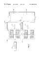
- FIG. 1 shows in block diagram form a computer system implementing context switching in accordance with the present invention
- FIG. 2 shows in block diagram form components of a context switching apparatus in accordance with the present invention.
- FIG. 1 illustrates in block diagram form a computer system incorporating an apparatus and system in accordance with the present invention.
- Processor architectures and computing systems are usefully represented as a collection of interacting functional units as shown in FIG. 1 . These functional units, discussed in greater detail below, perform the functions of fetching instructions and data from memory, processing fetched instructions, managing memory transactions, interfacing with external I/O and displaying information.
- FIG. 1 shows a typical general purpose computer system 100 incorporating a processor 102 and implementing both an application program and an operating system executing in processor 102 .
- Computer system 100 in accordance with the present invention comprises a system bus 101 for communicating information, processor 102 coupled with bus 101 through input/output (I/O) devices within processor 102 .
- Processor 102 is coupled to memory system 107 using a memory bus 103 to store information and instructions for processor 102 .
- Memory system 107 comprises, for example, one or more levels of cache memory and main memory in memory unit 107 . It should be understood that some cache memory is included on-chip with processor 102 in most applications in addition to cache and memory in memory system 107 .
- User I/O devices 106 are coupled to bus 101 and are operative to communicate information in appropriately structured form to and from the other parts of computer 100 .
- User I/O devices may include a keyboard, mouse, magnetic or tape reader, optical disk, or other available I/O devices, including another computer.
- Mass storage device 117 is coupled to bus 101 and may be implemented using one or more magnetic hard disks, magnetic tapes, CD ROMs, large banks of random access memory, or the like. A wide variety of random access and read-only memory technologies are available and are equivalent for purposes of the present invention. Mass storage 117 includes computer programs and data stored therein. Some or all of mass storage 117 may be configured to be incorporated as part of memory system 107 .
- Processor 102 includes a number of registers 203 (shown in FIG. 2) that are typically implemented in hardware. Data processing occurs by loading data into registers 203 , modifying data in registers 203 , and storing data from registers 203 back out to memory 107
- a processor 102 with a large general register file 202 (e.g., 256 registers) carries with this the potential for 512 memory operations on a context switch. Many of these will be unnecessary and so may lengthen the context switch time considerately.
- the present invention seeks to reduce this time by only loading and saving registers that are in fact needed, and to perform the saving operations in parallel with other instructions.
- an execution unit 201 within processor 102 accesses (i.e., loads, stores, and modifies) data stored in general register file 202 .
- General register file 202 comprises a plurality of registers 203 where the number of registers 203 is specified by the processor architecture.
- Each register 203 includes at least one, and typically more than one storage cell(s) each storing one bit of information.
- the registers 203 in general register file 202 are alternatively referred to as “architectural” register files.
- Each register 203 is accessible by execution unit 201 to enable processor 102 to load data from a selected register 203 and store data to a selected register 203 .
- registers 203 in aggregate define a “context” or the processor state during execution of a particular program thread or process.
- the context is saved persistently in memory 107 in a register save area 209 a or 209 b so that it can be restored on demand.
- register save areas 209 a and 209 b are shown, each context has a corresponding save area 209 .
- a current register file save area (RFSA) register 204 contains data pointing to an area of memory 107 where the current thread's register values are saved.
- the term “current thread” means a program thread currently executing in execution unit 201 .
- RFSA 204 contains a pointer to a start location or first memory location of a sequentially block of memory holding all of the values from registers 203 . Where the number of registers 203 in register file 202 is specified by the processor architecture, only the first register address is needed to access all of the registers 203 individually. Alternatively, the register values can be accessed from memory 107 in groups comprising some but less than all of the registers. A new value is written into current RFSA register 204 at the initiation of a context switch.
- each of registers 203 include or is associated with a valid bit (labeled “V” in FIG. 2) indicating whether data of the register is effective data or not.
- V a valid bit
- all the general registers 203 are marked as invalid. If a register 203 is written to when in the invalid state the associated valid bit is then marked valid.
- processor 102 When a register 203 is read while in the invalid state, processor 102 automatically loads the value from the register file save area 209 a of memory 107 . When the value is loaded, the corresponding valid bit is marked valid.
- Each register 203 is also associated with a dirty bit (labeled “D” in FIG. 2) that indicates that the value stored in the register file save area of memory 107 for that register 203 is out of sync with the current register 203 . Registers having a dirty bit set are referred to herein as “dirty registers”.
- shadow register file 207 may be implemented in a fashion so that each memory cell or storage location in each register 203 is physically adjacent to a corresponding memory cell or storage location in shadow register file 207 . In this manner, memory bus 103 is not burdened with the traffic required to copy all of registers 203 during a context switch.
- the content of each register 203 is copied together with its associated valid bit and dirty bit.
- registers values stored in shadow register 207 that are dirty as indicated by the dirty bit are written to the register save area 209 b in memory 107 using memory bus 103 at a location described by or derived from the value held in previous RFSA 206 .
- This “lazy” write back or commit of the register values in shadow register 207 makes efficient use of memory bus 103 and the available memory bus cycles.
- This function may be implemented without added processor instructions by hardware coupled to current RFSA register 204 to detect a change in current RFSA 204 value and coupled to shadow register 207 to detect whether any dirty bits are set in shadow register 207 .
- a context switch occurs, two cases may exist.
- a first case if the value of the new context in current RFSA 204 is the same as the value in the previous RFSA 206 , the register values in shadow register 207 and register file 202 can be swapped. In this case, it is not necessary to complete write back of all dirty registers in shadow register 207 to register save area 209 b .
- To enable swapping of the register values in may be desirable to include a third register file to temporarily hold the contents during swapping, although other hardware mechanisms to implement this swapping will be apparent to those skilled in the design of memory and processor systems.
- the value of the new context identified by the value stored in current RFSA 204 is different from the value in previous RFSA register 206 .
- all the registers having dirty bits currently set in shadow 207 (if any exist) must be saved to register save area 209 b in memory 107 before the context switch takes place.
- all of the dirty registers in shadow register 207 will have already been written back in free memory cycles.
- a forced write back is required. If the operating environment is such that frequent context switches occur with insufficient free memory clock cycles to complete the write back of dirty registers in shadow 207 , it may be desirable to steal memory cycles from the memory bus. The stolen memory cycles will impact normal operation, but will allow dirty registers in shadow register 207 to be completely written back before a subsequent context switch, resulting in a net improvement.
- shadow register 207 In most environments the write back of data from shadow register 207 to memory 107 will only write into a data cache. In uniprocessor environments it is acceptable for the contents of RFSA 209 b to be held in cache because the processor can readily access cached data. However, in SMP environments, all contents of shadow register 207 having the dirty bits set must eventually be written to memory 107 so that the data is available to other processors in the SMP system. To ensure that all the registers 203 are eventually written out to memory 107 , it may be necessary to force a cache write-back operation by issuing a commit instruction from time to time that writes all register values stored in cache to main memory. This commit instruction may be issued periodically or based upon elapsed time that the data has been in shadow register 207 , or frequency of context switches, other equivalent criteria, or a combination of these criteria.
- the new register values are loaded over memory bus 103 as needed from the associated register save area 209 a in memory 107 to register file 202 using the new value stored in current RFSA register 204 .
- This is alternatively referred to as a “lazy” restore, a “dynamic” restore, or a “just-in-time” restore.
- This is in contrast to existing systems that load the values into all of registers 203 before beginning to process data stored in register file 202 .
- the valid bits of each register 203 are marked invalid.
- execution unit 201 requests data for the first time from a register 203 , the value is automatically loaded from memory 107 (because the register 203 is marked invalid) .
- This dynamic restore feature of the present invention saves memory bus cycles that are ordinarily used to transfer register values that are not used by the executing thread.
- the dynamic loading feature enables execution unit 201 to process data from registers 203 faster than prior processors.
- the processor 102 in accordance with the present invention operates with greater efficiency.
- the method in accordance with the present invention carries an added advantage in a symmetric multi-processing (SMP) environment.
- SMP symmetric multi-processing
- a thread from a single threaded program may execute on different processors, each having distinct register file 202 .
- a CPU may attempt to execute a task that has not finished having its registers written back to memory on another CPU.
- shadow register file 207 will automatically synchronize with its associates register save area 209 b given sufficient time (i.e., sufficient available memory cycles) .
- Each register file save area desirably includes a flag 208 comprising a single bit to show that synchronization is complete (i.e., all registers in shadow register file 207 having a dirty bit have been written back to memory 107 .
- This bit flag 208 can be tested by a processor 102 that request to load the context stored in shadow register 207 .
Abstract
Description
Claims (22)
Priority Applications (2)
| Application Number | Priority Date | Filing Date | Title |
|---|---|---|---|
| US09/073,500 US6408325B1 (en) | 1998-05-06 | 1998-05-06 | Context switching technique for processors with large register files |
| EP99650039A EP0955583A3 (en) | 1998-05-06 | 1999-05-05 | Context switching technique for processors with large register files |
Applications Claiming Priority (1)
| Application Number | Priority Date | Filing Date | Title |
|---|---|---|---|
| US09/073,500 US6408325B1 (en) | 1998-05-06 | 1998-05-06 | Context switching technique for processors with large register files |
Publications (1)
| Publication Number | Publication Date |
|---|---|
| US6408325B1 true US6408325B1 (en) | 2002-06-18 |
Family
ID=22114052
Family Applications (1)
| Application Number | Title | Priority Date | Filing Date |
|---|---|---|---|
| US09/073,500 Expired - Lifetime US6408325B1 (en) | 1998-05-06 | 1998-05-06 | Context switching technique for processors with large register files |
Country Status (2)
| Country | Link |
|---|---|
| US (1) | US6408325B1 (en) |
| EP (1) | EP0955583A3 (en) |
Cited By (67)
| Publication number | Priority date | Publication date | Assignee | Title |
|---|---|---|---|---|
| US20020103979A1 (en) * | 2001-01-31 | 2002-08-01 | Matsushita Electric Industrial Co., Ltd. | Pointer register device and method for updating a pointer value |
| US20030041228A1 (en) * | 2001-08-27 | 2003-02-27 | Rosenbluth Mark B. | Multithreaded microprocessor with register allocation based on number of active threads |
| US20030065839A1 (en) * | 2001-09-28 | 2003-04-03 | Howard John S. | System and method for supporting split transactions on a bus |
| US20030145155A1 (en) * | 2002-01-25 | 2003-07-31 | Gilbert Wolrich | Data transfer mechanism |
| US20030149864A1 (en) * | 2002-01-09 | 2003-08-07 | Kazuya Furukawa | Processor and program execution method capable of efficient program execution |
| US20040015967A1 (en) * | 2002-05-03 | 2004-01-22 | Dale Morris | Method and system for application managed context switching |
| US20040034743A1 (en) * | 2002-08-13 | 2004-02-19 | Gilbert Wolrich | Free list and ring data structure management |
| US6704858B1 (en) * | 1999-06-09 | 2004-03-09 | Nec Electronics Corporation | Information processor and method for switching those register files |
| US20040128475A1 (en) * | 2002-12-31 | 2004-07-01 | Gad Sheaffer | Widely accessible processor register file and method for use |
| US20040221141A1 (en) * | 2003-02-17 | 2004-11-04 | Stmicroelectronics S.A. | Method for managing a microprocessor stack for saving contextual data |
| US20040230778A1 (en) * | 2003-05-16 | 2004-11-18 | Chou Yuan C. | Efficient register file checkpointing to facilitate speculative execution |
| US20050185437A1 (en) * | 2003-01-10 | 2005-08-25 | Gilbert Wolrich | Memory interleaving |
| US20050195199A1 (en) * | 2004-03-03 | 2005-09-08 | Anderson Michael H. | Depth buffer for rasterization pipeline |
| US20050216708A1 (en) * | 2004-03-24 | 2005-09-29 | Kabushiki Kaisha Toshiba | Processor for performing context switching, a method for performing context switching, a computer program for perform context switching |
| US20050251662A1 (en) * | 2004-04-22 | 2005-11-10 | Samra Nicholas G | Secondary register file mechanism for virtual multithreading |
| US7010674B2 (en) * | 1998-12-03 | 2006-03-07 | Sun Microsystems, Inc. | Efficient handling of a large register file for context switching and function calls and returns |
| US20060143485A1 (en) * | 2004-12-28 | 2006-06-29 | Alon Naveh | Techniques to manage power for a mobile device |
| US20060149940A1 (en) * | 2004-12-27 | 2006-07-06 | Intel Corporation | Implementation to save and restore processor registers on a context switch |
| US20070022428A1 (en) * | 2003-01-09 | 2007-01-25 | Japan Science And Technology Agency | Context switching method, device, program, recording medium, and central processing unit |
| US20070094484A1 (en) * | 2005-10-20 | 2007-04-26 | Bohuslav Rychlik | Backing store buffer for the register save engine of a stacked register file |
| US20070157036A1 (en) * | 2005-12-30 | 2007-07-05 | Intel Corporation | Method and apparatus for a zero voltage processor sleep state |
| US20070226474A1 (en) * | 2006-03-02 | 2007-09-27 | Samsung Electronics Co., Ltd. | Method and system for providing context switch using multiple register file |
| US7302452B2 (en) | 2003-06-05 | 2007-11-27 | International Business Machines Corporation | Method and apparatus for handling requests for files in a data processing system |
| US7310710B1 (en) * | 2003-03-11 | 2007-12-18 | Marvell International Ltd. | Register file with integrated routing to execution units for multi-threaded processors |
| US20080046701A1 (en) * | 2006-08-16 | 2008-02-21 | Arm Limited | Data processing apparatus and method for controlling access to registers |
| US20080104375A1 (en) * | 1995-08-16 | 2008-05-01 | Microunity Systems Engineering, Inc. | Programmable processor and method with wide operations |
| US20080133897A1 (en) * | 2006-10-24 | 2008-06-05 | Arm Limited | Diagnostic apparatus and method |
| US20080133898A1 (en) * | 2005-09-19 | 2008-06-05 | Newburn Chris J | Technique for context state management |
| US20080133899A1 (en) * | 2006-12-04 | 2008-06-05 | Samsung Electronics Co., Ltd. | Context switching method, medium, and system for reconfigurable processors |
| US20080270771A1 (en) * | 2007-04-30 | 2008-10-30 | National Tsing Hua University | Method of optimizing multi-set context switch for embedded processors |
| US20080307419A1 (en) * | 2007-06-06 | 2008-12-11 | Microsoft Corporation | Lazy kernel thread binding |
| US20080313440A1 (en) * | 2000-03-30 | 2008-12-18 | Transmeta Corporation | Switching to original code comparison of modifiable code for translated code validity when frequency of detecting memory overwrites exceeds threshold |
| US20080313656A1 (en) * | 2007-06-18 | 2008-12-18 | Microsoft Corporation | User mode stack disassociation |
| US20080320475A1 (en) * | 2007-06-19 | 2008-12-25 | Microsoft Corporation | Switching user mode thread context |
| US7478394B1 (en) * | 2001-06-04 | 2009-01-13 | Hewlett-Packard Development Company, L.P. | Context-corrupting context switching |
| US20090089562A1 (en) * | 2007-09-27 | 2009-04-02 | Ethan Schuchman | Methods and apparatuses for reducing power consumption of processor switch operations |
| US20090089540A1 (en) * | 1998-08-24 | 2009-04-02 | Microunity Systems Engineering, Inc. | Processor architecture for executing transfers between wide operand memories |
| US20090138880A1 (en) * | 2005-09-22 | 2009-05-28 | Andrei Igorevich Yafimau | Method for organizing a multi-processor computer |
| US7546444B1 (en) * | 1999-09-01 | 2009-06-09 | Intel Corporation | Register set used in multithreaded parallel processor architecture |
| US20090172298A1 (en) * | 2007-12-31 | 2009-07-02 | Yoon Ki W | Cached dirty bits for context switch consistency checks |
| US20090172675A1 (en) * | 2007-12-31 | 2009-07-02 | Advanced Micro Devices, Inc. | Re-Entrant Atomic Signaling |
| US7606363B1 (en) | 2005-07-26 | 2009-10-20 | Rockwell Collins, Inc. | System and method for context switching of a cryptographic engine |
| US20090282407A1 (en) * | 2003-03-13 | 2009-11-12 | Kunihiko Hayashi | Task switching apparatus, method and program |
| US7681018B2 (en) | 2000-08-31 | 2010-03-16 | Intel Corporation | Method and apparatus for providing large register address space while maximizing cycletime performance for a multi-threaded register file set |
| US7761857B1 (en) | 1999-10-13 | 2010-07-20 | Robert Bedichek | Method for switching between interpretation and dynamic translation in a processor system based upon code sequence execution counts |
| US20100217945A1 (en) * | 2009-02-26 | 2010-08-26 | International Business Machines Corporation | Fast context save in transactional memory |
| US20100287358A1 (en) * | 2009-05-05 | 2010-11-11 | International Business Machines Corporation | Branch Prediction Path Instruction |
| US7844804B2 (en) * | 2005-11-10 | 2010-11-30 | Qualcomm Incorporated | Expansion of a stacked register file using shadow registers |
| US7932911B2 (en) | 1998-08-24 | 2011-04-26 | Microunity Systems Engineering, Inc. | Processor for executing switch and translate instructions requiring wide operands |
| US7937710B1 (en) * | 2005-11-22 | 2011-05-03 | Nvidia Corporation | Context switch signaling method and system |
| US8019983B1 (en) | 2003-04-02 | 2011-09-13 | Rozas Guillermo J | Setting a flag bit to defer event handling to a safe point in an instruction stream |
| US20110225401A1 (en) * | 2010-03-11 | 2011-09-15 | International Business Machines Corporation | Prefetching branch prediction mechanisms |
| US8131982B2 (en) * | 2008-06-13 | 2012-03-06 | International Business Machines Corporation | Branch prediction instructions having mask values involving unloading and loading branch history data |
| US8413162B1 (en) * | 2005-06-28 | 2013-04-02 | Guillermo J. Rozas | Multi-threading based on rollback |
| US8631261B2 (en) * | 2007-12-31 | 2014-01-14 | Intel Corporation | Context state management for processor feature sets |
| US20160246728A1 (en) * | 2015-02-19 | 2016-08-25 | Apple Inc. | Register caching techniques for thread switches |
| US20160371082A1 (en) * | 2015-06-22 | 2016-12-22 | Advanced Micro Devices, Inc. | Instruction context switching |
| US9785565B2 (en) | 2014-06-30 | 2017-10-10 | Microunity Systems Engineering, Inc. | System and methods for expandably wide processor instructions |
| US10078518B2 (en) | 2012-11-01 | 2018-09-18 | International Business Machines Corporation | Intelligent context management |
| US10102003B2 (en) | 2012-11-01 | 2018-10-16 | International Business Machines Corporation | Intelligent context management |
| US10318302B2 (en) * | 2016-06-03 | 2019-06-11 | Synopsys, Inc. | Thread switching in microprocessor without full save and restore of register file |
| US10552158B2 (en) | 2016-08-18 | 2020-02-04 | Synopsys, Inc. | Reorder buffer scoreboard having multiple valid bits to indicate a location of data |
| US10558463B2 (en) | 2016-06-03 | 2020-02-11 | Synopsys, Inc. | Communication between threads of multi-thread processor |
| US10613859B2 (en) | 2016-08-18 | 2020-04-07 | Synopsys, Inc. | Triple-pass execution using a retire queue having a functional unit to independently execute long latency instructions and dependent instructions |
| US10628320B2 (en) | 2016-06-03 | 2020-04-21 | Synopsys, Inc. | Modulization of cache structure utilizing independent tag array and data array in microprocessor |
| CN112463327A (en) * | 2020-11-25 | 2021-03-09 | 海光信息技术股份有限公司 | Method and device for quickly switching logic threads, CPU chip and server |
| US11003488B2 (en) | 2019-05-03 | 2021-05-11 | Dell Products L.P. | Memory-fabric-based processor context switching system |
Families Citing this family (10)
| Publication number | Priority date | Publication date | Assignee | Title |
|---|---|---|---|---|
| AU2001257323A1 (en) * | 2000-04-27 | 2001-11-07 | Sun Microsystems, Inc. | Method and apparatus to improve context switch times in a computing system |
| DE10102202A1 (en) * | 2001-01-18 | 2002-08-08 | Infineon Technologies Ag | Microprocessor circuit for portable data carriers |
| US8042116B2 (en) | 2004-09-17 | 2011-10-18 | Panasonic Corporation | Task switching based on the execution control information held in register groups |
| US20070055839A1 (en) * | 2005-09-06 | 2007-03-08 | Alcatel | Processing operation information transfer control systems and methods |
| US9231595B2 (en) | 2013-06-12 | 2016-01-05 | International Business Machines Corporation | Filtering event log entries |
| JP2017037370A (en) * | 2015-08-06 | 2017-02-16 | 富士通株式会社 | Computing device, process control method and process control program |
| US10496437B2 (en) | 2017-11-14 | 2019-12-03 | International Business Machines Corporation | Context switch by changing memory pointers |
| US10558366B2 (en) | 2017-11-14 | 2020-02-11 | International Business Machines Corporation | Automatic pinning of units of memory |
| US10592164B2 (en) | 2017-11-14 | 2020-03-17 | International Business Machines Corporation | Portions of configuration state registers in-memory |
| US10403351B1 (en) * | 2018-02-22 | 2019-09-03 | Advanced Micro Devices, Inc. | Save and restore scoreboard |
Citations (12)
| Publication number | Priority date | Publication date | Assignee | Title |
|---|---|---|---|---|
| US4594660A (en) | 1982-10-13 | 1986-06-10 | Honeywell Information Systems Inc. | Collector |
| EP0285310A2 (en) | 1987-03-31 | 1988-10-05 | Kabushiki Kaisha Toshiba | Device for saving and restoring register information |
| EP0373790A2 (en) | 1988-11-30 | 1990-06-20 | Kabushiki Kaisha Toshiba | Data processing apparatus for saving and restoring |
| US5349680A (en) | 1990-11-07 | 1994-09-20 | Kabushiki Kaisha Toshiba | Information processing apparatus for executing application programs under control of a system program |
| US5448707A (en) * | 1991-10-29 | 1995-09-05 | Intel Corporation | Mechanism to protect data saved on a local register cache during inter-subsystem calls and returns |
| US5812868A (en) * | 1996-09-16 | 1998-09-22 | Motorola Inc. | Method and apparatus for selecting a register file in a data processing system |
| US5933627A (en) * | 1996-07-01 | 1999-08-03 | Sun Microsystems | Thread switch on blocked load or store using instruction thread field |
| US5966529A (en) * | 1995-05-15 | 1999-10-12 | Zsp Corporation | Processor having auxiliary operand register file and complementary arrangements for non-disruptively performing adjunct execution |
| US5974512A (en) * | 1996-02-07 | 1999-10-26 | Nec Corporation | System for saving and restoring contents of a plurality of registers |
| US6128728A (en) * | 1997-08-01 | 2000-10-03 | Micron Technology, Inc. | Virtual shadow registers and virtual register windows |
| US6223208B1 (en) * | 1997-10-03 | 2001-04-24 | International Business Machines Corporation | Moving data in and out of processor units using idle register/storage functional units |
| US6233599B1 (en) * | 1997-07-10 | 2001-05-15 | International Business Machines Corporation | Apparatus and method for retrofitting multi-threaded operations on a computer by partitioning and overlapping registers |
-
1998
- 1998-05-06 US US09/073,500 patent/US6408325B1/en not_active Expired - Lifetime
-
1999
- 1999-05-05 EP EP99650039A patent/EP0955583A3/en not_active Withdrawn
Patent Citations (13)
| Publication number | Priority date | Publication date | Assignee | Title |
|---|---|---|---|---|
| US4594660A (en) | 1982-10-13 | 1986-06-10 | Honeywell Information Systems Inc. | Collector |
| EP0285310A2 (en) | 1987-03-31 | 1988-10-05 | Kabushiki Kaisha Toshiba | Device for saving and restoring register information |
| US5021993A (en) | 1987-03-31 | 1991-06-04 | Kabushiki Kaisha Toshiba | Device for saving and restoring register information |
| EP0373790A2 (en) | 1988-11-30 | 1990-06-20 | Kabushiki Kaisha Toshiba | Data processing apparatus for saving and restoring |
| US5349680A (en) | 1990-11-07 | 1994-09-20 | Kabushiki Kaisha Toshiba | Information processing apparatus for executing application programs under control of a system program |
| US5448707A (en) * | 1991-10-29 | 1995-09-05 | Intel Corporation | Mechanism to protect data saved on a local register cache during inter-subsystem calls and returns |
| US5966529A (en) * | 1995-05-15 | 1999-10-12 | Zsp Corporation | Processor having auxiliary operand register file and complementary arrangements for non-disruptively performing adjunct execution |
| US5974512A (en) * | 1996-02-07 | 1999-10-26 | Nec Corporation | System for saving and restoring contents of a plurality of registers |
| US5933627A (en) * | 1996-07-01 | 1999-08-03 | Sun Microsystems | Thread switch on blocked load or store using instruction thread field |
| US5812868A (en) * | 1996-09-16 | 1998-09-22 | Motorola Inc. | Method and apparatus for selecting a register file in a data processing system |
| US6233599B1 (en) * | 1997-07-10 | 2001-05-15 | International Business Machines Corporation | Apparatus and method for retrofitting multi-threaded operations on a computer by partitioning and overlapping registers |
| US6128728A (en) * | 1997-08-01 | 2000-10-03 | Micron Technology, Inc. | Virtual shadow registers and virtual register windows |
| US6223208B1 (en) * | 1997-10-03 | 2001-04-24 | International Business Machines Corporation | Moving data in and out of processor units using idle register/storage functional units |
Non-Patent Citations (7)
| Title |
|---|
| "Technique for Reducing the Number of Registers Saved at a Context Swap", IBM Technical Disclosure Bulletin, vol. 33, No. 3A, Aug. 1990, pp. 234-235. |
| Cheng et al. The Compiler for Supporting Multithreading in Cyclic Register Windows, IEEE 1996.* * |
| Desai, S.M., "General Purpose Registers Extension", IBM Technical Disclosure Bulletin, vol. 24, No. 3, Aug. 1981, pp. 1404-1405. |
| Hidaka et al. Multiple Threads in Cyclic Register Windows 1993.* * |
| Keppel Register Windows and User-Space Threads on SPRAC 1991.* * |
| McGeady et al, Performance Enhancements in Superscalar; 960MM Embedded Mienpoons, 1991.* * |
| Waldspurger et al. Register Relocation: Flexible Contexts for Multithreading 1993.* * |
Cited By (145)
| Publication number | Priority date | Publication date | Assignee | Title |
|---|---|---|---|---|
| US20080104375A1 (en) * | 1995-08-16 | 2008-05-01 | Microunity Systems Engineering, Inc. | Programmable processor and method with wide operations |
| US7932910B2 (en) | 1995-08-16 | 2011-04-26 | Microunity Systems Engineering, Inc. | System and software for performing matrix multiply extract operations |
| US20110107069A1 (en) * | 1995-08-16 | 2011-05-05 | Microunity Systems Engineering, Inc. | Processor Architecture for Executing Wide Transform Slice Instructions |
| US7948496B2 (en) | 1998-08-24 | 2011-05-24 | Microunity Systems Engineering, Inc. | Processor architecture with wide operand cache |
| US20090089540A1 (en) * | 1998-08-24 | 2009-04-02 | Microunity Systems Engineering, Inc. | Processor architecture for executing transfers between wide operand memories |
| US7940277B2 (en) | 1998-08-24 | 2011-05-10 | Microunity Systems Engineering, Inc. | Processor for executing extract controlled by a register instruction |
| US20090113176A1 (en) * | 1998-08-24 | 2009-04-30 | Microunity Systems Engineering, Inc. | Method of reducing data path width restrictions on instruction sets |
| US20090113187A1 (en) * | 1998-08-24 | 2009-04-30 | Microunity Systems Engineering, Inc. | Processor architecture for executing instructions using wide operands |
| US8018464B2 (en) * | 1998-08-24 | 2011-09-13 | Microunity Systems Engineering, Inc. | Computer system for executing switch and table translate instructions requiring wide operands |
| US20090113185A1 (en) * | 1998-08-24 | 2009-04-30 | Microunity Systems Engineering, Inc. | Processor for executing multiply matrix and convolve extract instructions requiring wide operands |
| US10365926B2 (en) | 1998-08-24 | 2019-07-30 | Microunity Systems Engineering, Inc. | Processor and method for executing wide operand multiply matrix operations |
| US20090106536A1 (en) * | 1998-08-24 | 2009-04-23 | Microunity Systems Engineering, Inc. | Processor for executing group extract instructions requiring wide operands |
| US20090100227A1 (en) * | 1998-08-24 | 2009-04-16 | Microunity Systems Engineering, Inc. | Processor architecture with wide operand cache |
| US9378018B2 (en) | 1998-08-24 | 2016-06-28 | Microunity Systems Engineering, Inc. | Processor for executing wide operand operations using a control register and a results register |
| US9229713B2 (en) | 1998-08-24 | 2016-01-05 | Microunity Systems Engineering, Inc. | Processor for executing wide operand operations using a control register and a results register |
| US8812821B2 (en) | 1998-08-24 | 2014-08-19 | Microunity Systems Engineering, Inc. | Processor for performing operations with two wide operands |
| US7952587B2 (en) | 1998-08-24 | 2011-05-31 | Microunity Systems Engineering, Inc. | Processor and method for executing instructions requiring wide operands for multiply matrix operations |
| US7932911B2 (en) | 1998-08-24 | 2011-04-26 | Microunity Systems Engineering, Inc. | Processor for executing switch and translate instructions requiring wide operands |
| US7843459B2 (en) | 1998-08-24 | 2010-11-30 | Microunity Systems Engineering, Inc. | Processor for executing multiply matrix instructions requiring wide operands |
| US8269784B2 (en) | 1998-08-24 | 2012-09-18 | Microunity Systems Engineering, Inc. | Processor architecture for executing wide transform slice instructions |
| US7889204B2 (en) | 1998-08-24 | 2011-02-15 | Microunity Systems Engineering, Inc. | Processor architecture for executing wide transform slice instructions |
| US20090031105A1 (en) * | 1998-08-24 | 2009-01-29 | Microunity Systems Engineering, Inc. | Processor for executing group instructions requiring wide operands |
| US20060242388A1 (en) * | 1998-12-03 | 2006-10-26 | Sun Microsystems, Inc. | Processor with register dirty bit tracking for efficient context switch |
| US7490228B2 (en) * | 1998-12-03 | 2009-02-10 | Sun Microsystems, Inc. | Processor with register dirty bit tracking for efficient context switch |
| US7010674B2 (en) * | 1998-12-03 | 2006-03-07 | Sun Microsystems, Inc. | Efficient handling of a large register file for context switching and function calls and returns |
| US6704858B1 (en) * | 1999-06-09 | 2004-03-09 | Nec Electronics Corporation | Information processor and method for switching those register files |
| US7546444B1 (en) * | 1999-09-01 | 2009-06-09 | Intel Corporation | Register set used in multithreaded parallel processor architecture |
| US7991983B2 (en) | 1999-09-01 | 2011-08-02 | Intel Corporation | Register set used in multithreaded parallel processor architecture |
| US8418153B2 (en) | 1999-10-13 | 2013-04-09 | Robert Bedichek | Method for integration of interpretation and translation in a microprocessor |
| US7761857B1 (en) | 1999-10-13 | 2010-07-20 | Robert Bedichek | Method for switching between interpretation and dynamic translation in a processor system based upon code sequence execution counts |
| US20100262955A1 (en) * | 1999-10-13 | 2010-10-14 | Robert Bedichek | Method for integration of interpretation and translation in a microprocessor |
| US20080313440A1 (en) * | 2000-03-30 | 2008-12-18 | Transmeta Corporation | Switching to original code comparison of modifiable code for translated code validity when frequency of detecting memory overwrites exceeds threshold |
| US8438548B2 (en) | 2000-03-30 | 2013-05-07 | John Banning | Consistency checking of source instruction to execute previously translated instructions between copy made upon occurrence of write operation to memory and current version |
| US7904891B2 (en) | 2000-03-30 | 2011-03-08 | John Banning | Checking for instruction invariance to execute previously obtained translation code by comparing instruction to a copy stored when write operation to the memory portion occur |
| US7681018B2 (en) | 2000-08-31 | 2010-03-16 | Intel Corporation | Method and apparatus for providing large register address space while maximizing cycletime performance for a multi-threaded register file set |
| US7743235B2 (en) | 2000-08-31 | 2010-06-22 | Intel Corporation | Processor having a dedicated hash unit integrated within |
| US6665770B2 (en) * | 2001-01-31 | 2003-12-16 | Matsushita Electric Industrial Co., Ltd. | Device and method for updating a pointer value by switching between pointer values |
| US20020103979A1 (en) * | 2001-01-31 | 2002-08-01 | Matsushita Electric Industrial Co., Ltd. | Pointer register device and method for updating a pointer value |
| US7478394B1 (en) * | 2001-06-04 | 2009-01-13 | Hewlett-Packard Development Company, L.P. | Context-corrupting context switching |
| US20030041228A1 (en) * | 2001-08-27 | 2003-02-27 | Rosenbluth Mark B. | Multithreaded microprocessor with register allocation based on number of active threads |
| US7007119B2 (en) * | 2001-09-28 | 2006-02-28 | Intel Corporation | System and method for supporting split transactions on a bus |
| US20030065839A1 (en) * | 2001-09-28 | 2003-04-03 | Howard John S. | System and method for supporting split transactions on a bus |
| US20080209192A1 (en) * | 2002-01-09 | 2008-08-28 | Kazuya Furukawa | Processor and program execution method capable of efficient program execution |
| US8719827B2 (en) | 2002-01-09 | 2014-05-06 | Panasonic Corporation | Processor and program execution method capable of efficient program execution |
| US7386707B2 (en) * | 2002-01-09 | 2008-06-10 | Matsushita Electric Industrial Co., Ltd. | Processor and program execution method capable of efficient program execution |
| US8006076B2 (en) * | 2002-01-09 | 2011-08-23 | Panasonic Corporation | Processor and program execution method capable of efficient program execution |
| US20030149864A1 (en) * | 2002-01-09 | 2003-08-07 | Kazuya Furukawa | Processor and program execution method capable of efficient program execution |
| US9823946B2 (en) | 2002-01-09 | 2017-11-21 | Socionext Inc. | Processor and program execution method capable of efficient program execution |
| US7921281B2 (en) * | 2002-01-09 | 2011-04-05 | Panasonic Corporation | Processor and program execution method capable of efficient program execution |
| US20080209162A1 (en) * | 2002-01-09 | 2008-08-28 | Kazuya Furukawa | Processor and program execution method capable of efficient program execution |
| US20030145155A1 (en) * | 2002-01-25 | 2003-07-31 | Gilbert Wolrich | Data transfer mechanism |
| US7610451B2 (en) * | 2002-01-25 | 2009-10-27 | Intel Corporation | Data transfer mechanism using unidirectional pull bus and push bus |
| KR100895536B1 (en) * | 2002-01-25 | 2009-04-30 | 인텔 코포레이션 | Data transfer mechanism |
| US7523455B2 (en) * | 2002-05-03 | 2009-04-21 | Hewlett-Packard Development Company, L.P. | Method and system for application managed context switching |
| US20040015967A1 (en) * | 2002-05-03 | 2004-01-22 | Dale Morris | Method and system for application managed context switching |
| US20040034743A1 (en) * | 2002-08-13 | 2004-02-19 | Gilbert Wolrich | Free list and ring data structure management |
| US20040128475A1 (en) * | 2002-12-31 | 2004-07-01 | Gad Sheaffer | Widely accessible processor register file and method for use |
| US8020169B2 (en) * | 2003-01-09 | 2011-09-13 | Japan Science And Technology Agency | Context switching system having context cache and a register file for the save and restore context operation |
| US20070022428A1 (en) * | 2003-01-09 | 2007-01-25 | Japan Science And Technology Agency | Context switching method, device, program, recording medium, and central processing unit |
| US20050185437A1 (en) * | 2003-01-10 | 2005-08-25 | Gilbert Wolrich | Memory interleaving |
| US7421570B2 (en) * | 2003-02-17 | 2008-09-02 | Stmicroelectronics, Sa | Method for managing a microprocessor stack for saving contextual data |
| US20040221141A1 (en) * | 2003-02-17 | 2004-11-04 | Stmicroelectronics S.A. | Method for managing a microprocessor stack for saving contextual data |
| US7600084B1 (en) | 2003-03-11 | 2009-10-06 | Marvell International Ltd. | Register file with integrated routing to execution units for multi-threaded processors |
| US7310710B1 (en) * | 2003-03-11 | 2007-12-18 | Marvell International Ltd. | Register file with integrated routing to execution units for multi-threaded processors |
| US20090282407A1 (en) * | 2003-03-13 | 2009-11-12 | Kunihiko Hayashi | Task switching apparatus, method and program |
| US7735087B2 (en) | 2003-03-13 | 2010-06-08 | Panasonic Corporation | Task switching apparatus, method and program |
| US8276156B2 (en) | 2003-03-13 | 2012-09-25 | Panasonic Corporation | Task switching based on assigned time slot |
| US7950016B2 (en) | 2003-03-13 | 2011-05-24 | Panasonic Corporation | Apparatus for switching the task to be completed in a processor by switching to the task assigned time slot |
| US8464033B2 (en) | 2003-04-02 | 2013-06-11 | Guillermo J. Rozas | Setting a flag bit to defer event handling to one of multiple safe points in an instruction stream |
| US8019983B1 (en) | 2003-04-02 | 2011-09-13 | Rozas Guillermo J | Setting a flag bit to defer event handling to a safe point in an instruction stream |
| US7475230B2 (en) * | 2003-05-16 | 2009-01-06 | Sun Microsystems, Inc. | Method and apparatus for performing register file checkpointing to support speculative execution within a processor |
| US20040230778A1 (en) * | 2003-05-16 | 2004-11-18 | Chou Yuan C. | Efficient register file checkpointing to facilitate speculative execution |
| US7302452B2 (en) | 2003-06-05 | 2007-11-27 | International Business Machines Corporation | Method and apparatus for handling requests for files in a data processing system |
| US8081182B2 (en) * | 2004-03-03 | 2011-12-20 | Qualcomm Incorporated | Depth buffer for rasterization pipeline |
| US20050195199A1 (en) * | 2004-03-03 | 2005-09-08 | Anderson Michael H. | Depth buffer for rasterization pipeline |
| US20050216708A1 (en) * | 2004-03-24 | 2005-09-29 | Kabushiki Kaisha Toshiba | Processor for performing context switching, a method for performing context switching, a computer program for perform context switching |
| US20050251662A1 (en) * | 2004-04-22 | 2005-11-10 | Samra Nicholas G | Secondary register file mechanism for virtual multithreading |
| US9141180B2 (en) | 2004-07-27 | 2015-09-22 | Intel Corporation | Method and apparatus for a zero voltage processor sleep state |
| US9223390B2 (en) | 2004-07-27 | 2015-12-29 | Intel Corporation | Method and apparatus for a zero voltage processor |
| US9235258B2 (en) | 2004-07-27 | 2016-01-12 | Intel Corporation | Method and apparatus for a zero voltage processor |
| US9870044B2 (en) | 2004-07-27 | 2018-01-16 | Intel Corporation | Method and apparatus for a zero voltage processor sleep state |
| US9841807B2 (en) | 2004-07-27 | 2017-12-12 | Intel Corporation | Method and apparatus for a zero voltage processor sleep state |
| US9081575B2 (en) | 2004-07-27 | 2015-07-14 | Intel Corporation | Method and apparatus for a zero voltage processor sleep state |
| US9223389B2 (en) | 2004-07-27 | 2015-12-29 | Intel Corporation | Method and apparatus for a zero voltage processor |
| US20060149940A1 (en) * | 2004-12-27 | 2006-07-06 | Intel Corporation | Implementation to save and restore processor registers on a context switch |
| US20060143485A1 (en) * | 2004-12-28 | 2006-06-29 | Alon Naveh | Techniques to manage power for a mobile device |
| US8413162B1 (en) * | 2005-06-28 | 2013-04-02 | Guillermo J. Rozas | Multi-threading based on rollback |
| US7606363B1 (en) | 2005-07-26 | 2009-10-20 | Rockwell Collins, Inc. | System and method for context switching of a cryptographic engine |
| US8171268B2 (en) * | 2005-09-19 | 2012-05-01 | Intel Corporation | Technique for context state management to reduce save and restore operations between a memory and a processor using in-use vectors |
| US20080133898A1 (en) * | 2005-09-19 | 2008-06-05 | Newburn Chris J | Technique for context state management |
| US20090138880A1 (en) * | 2005-09-22 | 2009-05-28 | Andrei Igorevich Yafimau | Method for organizing a multi-processor computer |
| US20070094484A1 (en) * | 2005-10-20 | 2007-04-26 | Bohuslav Rychlik | Backing store buffer for the register save engine of a stacked register file |
| US7962731B2 (en) * | 2005-10-20 | 2011-06-14 | Qualcomm Incorporated | Backing store buffer for the register save engine of a stacked register file |
| JP2014130606A (en) * | 2005-10-20 | 2014-07-10 | Qualcomm Incorporated | Backing store buffer for register save engine of stacked register file |
| US7844804B2 (en) * | 2005-11-10 | 2010-11-30 | Qualcomm Incorporated | Expansion of a stacked register file using shadow registers |
| US7937710B1 (en) * | 2005-11-22 | 2011-05-03 | Nvidia Corporation | Context switch signaling method and system |
| US20080072088A1 (en) * | 2005-12-30 | 2008-03-20 | Jose Allarey | Method and Apparatus for a Zero Voltage Processor Sleep State |
| US20070157036A1 (en) * | 2005-12-30 | 2007-07-05 | Intel Corporation | Method and apparatus for a zero voltage processor sleep state |
| US8707062B2 (en) | 2005-12-30 | 2014-04-22 | Intel Corporation | Method and apparatus for powered off processor core mode |
| US20100146311A1 (en) * | 2005-12-30 | 2010-06-10 | Intel Corporation | Method and Apparatus for a Zero Voltage Processor Sleep State |
| US7953993B2 (en) | 2005-12-30 | 2011-05-31 | Intel Corporation | Method and apparatus for a zero voltage processor sleep state |
| US8707066B2 (en) | 2005-12-30 | 2014-04-22 | Intel Corporation | Method and apparatus for a zero voltage processor sleep state |
| US7664970B2 (en) | 2005-12-30 | 2010-02-16 | Intel Corporation | Method and apparatus for a zero voltage processor sleep state |
| US20110231681A1 (en) * | 2005-12-30 | 2011-09-22 | Jose Allarey | Method and apparatus for a zero voltage processor sleep state |
| US8327122B2 (en) * | 2006-03-02 | 2012-12-04 | Samsung Electronics Co., Ltd. | Method and system for providing context switch using multiple register file |
| US20070226474A1 (en) * | 2006-03-02 | 2007-09-27 | Samsung Electronics Co., Ltd. | Method and system for providing context switch using multiple register file |
| US7529916B2 (en) * | 2006-08-16 | 2009-05-05 | Arm Limited | Data processing apparatus and method for controlling access to registers |
| US20080046701A1 (en) * | 2006-08-16 | 2008-02-21 | Arm Limited | Data processing apparatus and method for controlling access to registers |
| US20080133897A1 (en) * | 2006-10-24 | 2008-06-05 | Arm Limited | Diagnostic apparatus and method |
| US20080133899A1 (en) * | 2006-12-04 | 2008-06-05 | Samsung Electronics Co., Ltd. | Context switching method, medium, and system for reconfigurable processors |
| US8407715B2 (en) * | 2007-04-30 | 2013-03-26 | National Tsing Hua University | Live range sensitive context switch procedure comprising a plurality of register sets associated with usage frequencies and live set information of tasks |
| US20080270771A1 (en) * | 2007-04-30 | 2008-10-30 | National Tsing Hua University | Method of optimizing multi-set context switch for embedded processors |
| US20080307419A1 (en) * | 2007-06-06 | 2008-12-11 | Microsoft Corporation | Lazy kernel thread binding |
| US20080313656A1 (en) * | 2007-06-18 | 2008-12-18 | Microsoft Corporation | User mode stack disassociation |
| US20080320475A1 (en) * | 2007-06-19 | 2008-12-25 | Microsoft Corporation | Switching user mode thread context |
| US20090089562A1 (en) * | 2007-09-27 | 2009-04-02 | Ethan Schuchman | Methods and apparatuses for reducing power consumption of processor switch operations |
| US8762692B2 (en) * | 2007-09-27 | 2014-06-24 | Intel Corporation | Single instruction for specifying and saving a subset of registers, specifying a pointer to a work-monitoring function to be executed after waking, and entering a low-power mode |
| US9600283B2 (en) | 2007-09-27 | 2017-03-21 | Intel Corporation | Single instruction for specifying a subset of registers to save prior to entering low-power mode, and for specifying a pointer to a function executed after exiting low-power mode |
| US9164764B2 (en) | 2007-09-27 | 2015-10-20 | Intel Corporation | Single instruction for specifying and saving a subset of registers, specifying a pointer to a work-monitoring function to be executed after waking, and entering a low-power mode |
| US20090172298A1 (en) * | 2007-12-31 | 2009-07-02 | Yoon Ki W | Cached dirty bits for context switch consistency checks |
| US8677163B2 (en) | 2007-12-31 | 2014-03-18 | Intel Corporation | Context state management for processor feature sets |
| US8261028B2 (en) * | 2007-12-31 | 2012-09-04 | Intel Corporation | Cached dirty bits for context switch consistency checks |
| US20090172675A1 (en) * | 2007-12-31 | 2009-07-02 | Advanced Micro Devices, Inc. | Re-Entrant Atomic Signaling |
| US8631261B2 (en) * | 2007-12-31 | 2014-01-14 | Intel Corporation | Context state management for processor feature sets |
| US8131982B2 (en) * | 2008-06-13 | 2012-03-06 | International Business Machines Corporation | Branch prediction instructions having mask values involving unloading and loading branch history data |
| US20100217945A1 (en) * | 2009-02-26 | 2010-08-26 | International Business Machines Corporation | Fast context save in transactional memory |
| US20100287358A1 (en) * | 2009-05-05 | 2010-11-11 | International Business Machines Corporation | Branch Prediction Path Instruction |
| US10338923B2 (en) | 2009-05-05 | 2019-07-02 | International Business Machines Corporation | Branch prediction path wrong guess instruction |
| US20110225401A1 (en) * | 2010-03-11 | 2011-09-15 | International Business Machines Corporation | Prefetching branch prediction mechanisms |
| US8521999B2 (en) | 2010-03-11 | 2013-08-27 | International Business Machines Corporation | Executing touchBHT instruction to pre-fetch information to prediction mechanism for branch with taken history |
| US10102003B2 (en) | 2012-11-01 | 2018-10-16 | International Business Machines Corporation | Intelligent context management |
| US10078518B2 (en) | 2012-11-01 | 2018-09-18 | International Business Machines Corporation | Intelligent context management |
| US9785565B2 (en) | 2014-06-30 | 2017-10-10 | Microunity Systems Engineering, Inc. | System and methods for expandably wide processor instructions |
| US10204055B2 (en) | 2014-06-30 | 2019-02-12 | Microunity Systems Engineering, Inc. | System and methods for expandably wide processor instructions |
| US20160246728A1 (en) * | 2015-02-19 | 2016-08-25 | Apple Inc. | Register caching techniques for thread switches |
| US9817664B2 (en) * | 2015-02-19 | 2017-11-14 | Apple Inc. | Register caching techniques for thread switches |
| US10019283B2 (en) * | 2015-06-22 | 2018-07-10 | Advanced Micro Devices, Inc. | Predicting a context portion to move between a context buffer and registers based on context portions previously used by at least one other thread |
| US20160371082A1 (en) * | 2015-06-22 | 2016-12-22 | Advanced Micro Devices, Inc. | Instruction context switching |
| US10318302B2 (en) * | 2016-06-03 | 2019-06-11 | Synopsys, Inc. | Thread switching in microprocessor without full save and restore of register file |
| US10558463B2 (en) | 2016-06-03 | 2020-02-11 | Synopsys, Inc. | Communication between threads of multi-thread processor |
| US10628320B2 (en) | 2016-06-03 | 2020-04-21 | Synopsys, Inc. | Modulization of cache structure utilizing independent tag array and data array in microprocessor |
| US10552158B2 (en) | 2016-08-18 | 2020-02-04 | Synopsys, Inc. | Reorder buffer scoreboard having multiple valid bits to indicate a location of data |
| US10613859B2 (en) | 2016-08-18 | 2020-04-07 | Synopsys, Inc. | Triple-pass execution using a retire queue having a functional unit to independently execute long latency instructions and dependent instructions |
| US11003488B2 (en) | 2019-05-03 | 2021-05-11 | Dell Products L.P. | Memory-fabric-based processor context switching system |
| CN112463327A (en) * | 2020-11-25 | 2021-03-09 | 海光信息技术股份有限公司 | Method and device for quickly switching logic threads, CPU chip and server |
Also Published As
| Publication number | Publication date |
|---|---|
| EP0955583A3 (en) | 2001-04-11 |
| EP0955583A2 (en) | 1999-11-10 |
Similar Documents
| Publication | Publication Date | Title |
|---|---|---|
| US6408325B1 (en) | Context switching technique for processors with large register files | |
| Shin et al. | Proteus: A flexible and fast software supported hardware logging approach for nvm | |
| KR101025354B1 (en) | Global overflow method for virtualized transactional memory | |
| US8688917B2 (en) | Read and write monitoring attributes in transactional memory (TM) systems | |
| US20180011748A1 (en) | Post-retire scheme for tracking tentative accesses during transactional execution | |
| KR100334479B1 (en) | Methods and apparatus for reordering load operations in a computer processing system | |
| US6272520B1 (en) | Method for detecting thread switch events | |
| JP3512678B2 (en) | Cache memory control device and computer system | |
| US9367472B2 (en) | Observation of data in persistent memory | |
| US7590774B2 (en) | Method and system for efficient context swapping | |
| US5944815A (en) | Microprocessor configured to execute a prefetch instruction including an access count field defining an expected number of access | |
| US5805879A (en) | In a pipelined processor, setting a segment access indicator during execution stage using exception handling | |
| US7584346B1 (en) | Method and apparatus for supporting different modes of multi-threaded speculative execution | |
| EP0541216B1 (en) | Data driven processing system | |
| JP3531167B2 (en) | System and method for assigning tags to instructions to control instruction execution | |
| US5596735A (en) | Circuit and method for addressing segment descriptor tables | |
| US11301142B2 (en) | Non-blocking flow control in multi-processing-entity systems | |
| US8806145B2 (en) | Methods and apparatuses for improving speculation success in processors | |
| US5941977A (en) | Apparatus for handling register windows in an out-of-order processor | |
| US5870597A (en) | Method for speculative calculation of physical register addresses in an out of order processor | |
| WO2001084304A2 (en) | Active address content addressable memory | |
| US5161219A (en) | Computer system with input/output cache | |
| US20060149940A1 (en) | Implementation to save and restore processor registers on a context switch | |
| Kopser et al. | Overview of the next generation Cray XMT | |
| US6631452B1 (en) | Register stack engine having speculative load/store modes |
Legal Events
| Date | Code | Title | Description |
|---|---|---|---|
| AS | Assignment |
Owner name: SUN MICROSYSTEMS, INC., CALIFORNIA Free format text: ASSIGNMENT OF ASSIGNORS INTEREST;ASSIGNOR:SHAYLOR, NIK;REEL/FRAME:009159/0057 Effective date: 19980429 |
|
| STCF | Information on status: patent grant |
Free format text: PATENTED CASE |
|
| CC | Certificate of correction | ||
| FPAY | Fee payment |
Year of fee payment: 4 |
|
| FPAY | Fee payment |
Year of fee payment: 8 |
|
| FPAY | Fee payment |
Year of fee payment: 12 |
|
| AS | Assignment |
Owner name: ORACLE AMERICA, INC., CALIFORNIA Free format text: MERGER AND CHANGE OF NAME;ASSIGNORS:ORACLE USA, INC.;SUN MICROSYSTEMS, INC.;ORACLE AMERICA, INC.;REEL/FRAME:037278/0612 Effective date: 20100212 |