US6418615B1 - Method of making multilayered substrate for semiconductor device - Google Patents
Method of making multilayered substrate for semiconductor device Download PDFInfo
- Publication number
- US6418615B1 US6418615B1 US09/523,149 US52314900A US6418615B1 US 6418615 B1 US6418615 B1 US 6418615B1 US 52314900 A US52314900 A US 52314900A US 6418615 B1 US6418615 B1 US 6418615B1
- Authority
- US
- United States
- Prior art keywords
- layer
- forming
- semiconductor element
- metal sheet
- metal
- Prior art date
- Legal status (The legal status is an assumption and is not a legal conclusion. Google has not performed a legal analysis and makes no representation as to the accuracy of the status listed.)
- Expired - Lifetime
Links
Images


Classifications
-
- H—ELECTRICITY
- H05—ELECTRIC TECHNIQUES NOT OTHERWISE PROVIDED FOR
- H05K—PRINTED CIRCUITS; CASINGS OR CONSTRUCTIONAL DETAILS OF ELECTRIC APPARATUS; MANUFACTURE OF ASSEMBLAGES OF ELECTRICAL COMPONENTS
- H05K3/00—Apparatus or processes for manufacturing printed circuits
- H05K3/46—Manufacturing multilayer circuits
- H05K3/4644—Manufacturing multilayer circuits by building the multilayer layer by layer, i.e. build-up multilayer circuits
- H05K3/4682—Manufacture of core-less build-up multilayer circuits on a temporary carrier or on a metal foil
-
- H—ELECTRICITY
- H01—ELECTRIC ELEMENTS
- H01L—SEMICONDUCTOR DEVICES NOT COVERED BY CLASS H10
- H01L21/00—Processes or apparatus adapted for the manufacture or treatment of semiconductor or solid state devices or of parts thereof
- H01L21/67—Apparatus specially adapted for handling semiconductor or electric solid state devices during manufacture or treatment thereof; Apparatus specially adapted for handling wafers during manufacture or treatment of semiconductor or electric solid state devices or components ; Apparatus not specifically provided for elsewhere
- H01L21/683—Apparatus specially adapted for handling semiconductor or electric solid state devices during manufacture or treatment thereof; Apparatus specially adapted for handling wafers during manufacture or treatment of semiconductor or electric solid state devices or components ; Apparatus not specifically provided for elsewhere for supporting or gripping
- H01L21/6835—Apparatus specially adapted for handling semiconductor or electric solid state devices during manufacture or treatment thereof; Apparatus specially adapted for handling wafers during manufacture or treatment of semiconductor or electric solid state devices or components ; Apparatus not specifically provided for elsewhere for supporting or gripping using temporarily an auxiliary support
-
- H—ELECTRICITY
- H01—ELECTRIC ELEMENTS
- H01L—SEMICONDUCTOR DEVICES NOT COVERED BY CLASS H10
- H01L23/00—Details of semiconductor or other solid state devices
- H01L23/48—Arrangements for conducting electric current to or from the solid state body in operation, e.g. leads, terminal arrangements ; Selection of materials therefor
- H01L23/488—Arrangements for conducting electric current to or from the solid state body in operation, e.g. leads, terminal arrangements ; Selection of materials therefor consisting of soldered or bonded constructions
- H01L23/498—Leads, i.e. metallisations or lead-frames on insulating substrates, e.g. chip carriers
- H01L23/49811—Additional leads joined to the metallisation on the insulating substrate, e.g. pins, bumps, wires, flat leads
-
- H—ELECTRICITY
- H01—ELECTRIC ELEMENTS
- H01L—SEMICONDUCTOR DEVICES NOT COVERED BY CLASS H10
- H01L23/00—Details of semiconductor or other solid state devices
- H01L23/48—Arrangements for conducting electric current to or from the solid state body in operation, e.g. leads, terminal arrangements ; Selection of materials therefor
- H01L23/488—Arrangements for conducting electric current to or from the solid state body in operation, e.g. leads, terminal arrangements ; Selection of materials therefor consisting of soldered or bonded constructions
- H01L23/498—Leads, i.e. metallisations or lead-frames on insulating substrates, e.g. chip carriers
- H01L23/49822—Multilayer substrates
-
- H—ELECTRICITY
- H05—ELECTRIC TECHNIQUES NOT OTHERWISE PROVIDED FOR
- H05K—PRINTED CIRCUITS; CASINGS OR CONSTRUCTIONAL DETAILS OF ELECTRIC APPARATUS; MANUFACTURE OF ASSEMBLAGES OF ELECTRICAL COMPONENTS
- H05K1/00—Printed circuits
- H05K1/02—Details
- H05K1/11—Printed elements for providing electric connections to or between printed circuits
- H05K1/111—Pads for surface mounting, e.g. lay-out
- H05K1/112—Pads for surface mounting, e.g. lay-out directly combined with via connections
- H05K1/113—Via provided in pad; Pad over filled via
-
- H—ELECTRICITY
- H01—ELECTRIC ELEMENTS
- H01L—SEMICONDUCTOR DEVICES NOT COVERED BY CLASS H10
- H01L2221/00—Processes or apparatus adapted for the manufacture or treatment of semiconductor or solid state devices or of parts thereof covered by H01L21/00
- H01L2221/67—Apparatus for handling semiconductor or electric solid state devices during manufacture or treatment thereof; Apparatus for handling wafers during manufacture or treatment of semiconductor or electric solid state devices or components; Apparatus not specifically provided for elsewhere
- H01L2221/683—Apparatus for handling semiconductor or electric solid state devices during manufacture or treatment thereof; Apparatus for handling wafers during manufacture or treatment of semiconductor or electric solid state devices or components; Apparatus not specifically provided for elsewhere for supporting or gripping
- H01L2221/68304—Apparatus for handling semiconductor or electric solid state devices during manufacture or treatment thereof; Apparatus for handling wafers during manufacture or treatment of semiconductor or electric solid state devices or components; Apparatus not specifically provided for elsewhere for supporting or gripping using temporarily an auxiliary support
- H01L2221/68345—Apparatus for handling semiconductor or electric solid state devices during manufacture or treatment thereof; Apparatus for handling wafers during manufacture or treatment of semiconductor or electric solid state devices or components; Apparatus not specifically provided for elsewhere for supporting or gripping using temporarily an auxiliary support used as a support during the manufacture of self supporting substrates
-
- H—ELECTRICITY
- H01—ELECTRIC ELEMENTS
- H01L—SEMICONDUCTOR DEVICES NOT COVERED BY CLASS H10
- H01L2224/00—Indexing scheme for arrangements for connecting or disconnecting semiconductor or solid-state bodies and methods related thereto as covered by H01L24/00
- H01L2224/01—Means for bonding being attached to, or being formed on, the surface to be connected, e.g. chip-to-package, die-attach, "first-level" interconnects; Manufacturing methods related thereto
- H01L2224/10—Bump connectors; Manufacturing methods related thereto
- H01L2224/15—Structure, shape, material or disposition of the bump connectors after the connecting process
- H01L2224/16—Structure, shape, material or disposition of the bump connectors after the connecting process of an individual bump connector
- H01L2224/161—Disposition
- H01L2224/16151—Disposition the bump connector connecting between a semiconductor or solid-state body and an item not being a semiconductor or solid-state body, e.g. chip-to-substrate, chip-to-passive
- H01L2224/16221—Disposition the bump connector connecting between a semiconductor or solid-state body and an item not being a semiconductor or solid-state body, e.g. chip-to-substrate, chip-to-passive the body and the item being stacked
- H01L2224/16225—Disposition the bump connector connecting between a semiconductor or solid-state body and an item not being a semiconductor or solid-state body, e.g. chip-to-substrate, chip-to-passive the body and the item being stacked the item being non-metallic, e.g. insulating substrate with or without metallisation
-
- H—ELECTRICITY
- H01—ELECTRIC ELEMENTS
- H01L—SEMICONDUCTOR DEVICES NOT COVERED BY CLASS H10
- H01L2924/00—Indexing scheme for arrangements or methods for connecting or disconnecting semiconductor or solid-state bodies as covered by H01L24/00
- H01L2924/01—Chemical elements
- H01L2924/01019—Potassium [K]
-
- H—ELECTRICITY
- H01—ELECTRIC ELEMENTS
- H01L—SEMICONDUCTOR DEVICES NOT COVERED BY CLASS H10
- H01L2924/00—Indexing scheme for arrangements or methods for connecting or disconnecting semiconductor or solid-state bodies as covered by H01L24/00
- H01L2924/01—Chemical elements
- H01L2924/01046—Palladium [Pd]
-
- H—ELECTRICITY
- H01—ELECTRIC ELEMENTS
- H01L—SEMICONDUCTOR DEVICES NOT COVERED BY CLASS H10
- H01L2924/00—Indexing scheme for arrangements or methods for connecting or disconnecting semiconductor or solid-state bodies as covered by H01L24/00
- H01L2924/01—Chemical elements
- H01L2924/01078—Platinum [Pt]
-
- H—ELECTRICITY
- H01—ELECTRIC ELEMENTS
- H01L—SEMICONDUCTOR DEVICES NOT COVERED BY CLASS H10
- H01L2924/00—Indexing scheme for arrangements or methods for connecting or disconnecting semiconductor or solid-state bodies as covered by H01L24/00
- H01L2924/01—Chemical elements
- H01L2924/01079—Gold [Au]
-
- H—ELECTRICITY
- H01—ELECTRIC ELEMENTS
- H01L—SEMICONDUCTOR DEVICES NOT COVERED BY CLASS H10
- H01L2924/00—Indexing scheme for arrangements or methods for connecting or disconnecting semiconductor or solid-state bodies as covered by H01L24/00
- H01L2924/15—Details of package parts other than the semiconductor or other solid state devices to be connected
- H01L2924/151—Die mounting substrate
- H01L2924/153—Connection portion
- H01L2924/1531—Connection portion the connection portion being formed only on the surface of the substrate opposite to the die mounting surface
- H01L2924/15311—Connection portion the connection portion being formed only on the surface of the substrate opposite to the die mounting surface being a ball array, e.g. BGA
-
- H—ELECTRICITY
- H01—ELECTRIC ELEMENTS
- H01L—SEMICONDUCTOR DEVICES NOT COVERED BY CLASS H10
- H01L2924/00—Indexing scheme for arrangements or methods for connecting or disconnecting semiconductor or solid-state bodies as covered by H01L24/00
- H01L2924/30—Technical effects
- H01L2924/301—Electrical effects
- H01L2924/3025—Electromagnetic shielding
-
- H—ELECTRICITY
- H05—ELECTRIC TECHNIQUES NOT OTHERWISE PROVIDED FOR
- H05K—PRINTED CIRCUITS; CASINGS OR CONSTRUCTIONAL DETAILS OF ELECTRIC APPARATUS; MANUFACTURE OF ASSEMBLAGES OF ELECTRICAL COMPONENTS
- H05K2201/00—Indexing scheme relating to printed circuits covered by H05K1/00
- H05K2201/09—Shape and layout
- H05K2201/09209—Shape and layout details of conductors
- H05K2201/095—Conductive through-holes or vias
- H05K2201/09509—Blind vias, i.e. vias having one side closed
- H05K2201/09527—Inverse blind vias, i.e. bottoms outwards in multilayer PCB; Blind vias in centre of PCB having opposed bottoms
-
- H—ELECTRICITY
- H05—ELECTRIC TECHNIQUES NOT OTHERWISE PROVIDED FOR
- H05K—PRINTED CIRCUITS; CASINGS OR CONSTRUCTIONAL DETAILS OF ELECTRIC APPARATUS; MANUFACTURE OF ASSEMBLAGES OF ELECTRICAL COMPONENTS
- H05K2201/00—Indexing scheme relating to printed circuits covered by H05K1/00
- H05K2201/09—Shape and layout
- H05K2201/09209—Shape and layout details of conductors
- H05K2201/095—Conductive through-holes or vias
- H05K2201/09563—Metal filled via
-
- H—ELECTRICITY
- H05—ELECTRIC TECHNIQUES NOT OTHERWISE PROVIDED FOR
- H05K—PRINTED CIRCUITS; CASINGS OR CONSTRUCTIONAL DETAILS OF ELECTRIC APPARATUS; MANUFACTURE OF ASSEMBLAGES OF ELECTRICAL COMPONENTS
- H05K2203/00—Indexing scheme relating to apparatus or processes for manufacturing printed circuits covered by H05K3/00
- H05K2203/01—Tools for processing; Objects used during processing
- H05K2203/0147—Carriers and holders
- H05K2203/0152—Temporary metallic carrier, e.g. for transferring material
-
- H—ELECTRICITY
- H05—ELECTRIC TECHNIQUES NOT OTHERWISE PROVIDED FOR
- H05K—PRINTED CIRCUITS; CASINGS OR CONSTRUCTIONAL DETAILS OF ELECTRIC APPARATUS; MANUFACTURE OF ASSEMBLAGES OF ELECTRICAL COMPONENTS
- H05K2203/00—Indexing scheme relating to apparatus or processes for manufacturing printed circuits covered by H05K3/00
- H05K2203/03—Metal processing
- H05K2203/0376—Etching temporary metallic carrier substrate
-
- H—ELECTRICITY
- H05—ELECTRIC TECHNIQUES NOT OTHERWISE PROVIDED FOR
- H05K—PRINTED CIRCUITS; CASINGS OR CONSTRUCTIONAL DETAILS OF ELECTRIC APPARATUS; MANUFACTURE OF ASSEMBLAGES OF ELECTRICAL COMPONENTS
- H05K2203/00—Indexing scheme relating to apparatus or processes for manufacturing printed circuits covered by H05K3/00
- H05K2203/03—Metal processing
- H05K2203/0384—Etch stop layer, i.e. a buried barrier layer for preventing etching of layers under the etch stop layer
-
- H—ELECTRICITY
- H05—ELECTRIC TECHNIQUES NOT OTHERWISE PROVIDED FOR
- H05K—PRINTED CIRCUITS; CASINGS OR CONSTRUCTIONAL DETAILS OF ELECTRIC APPARATUS; MANUFACTURE OF ASSEMBLAGES OF ELECTRICAL COMPONENTS
- H05K3/00—Apparatus or processes for manufacturing printed circuits
- H05K3/007—Manufacture or processing of a substrate for a printed circuit board supported by a temporary or sacrificial carrier
-
- H—ELECTRICITY
- H05—ELECTRIC TECHNIQUES NOT OTHERWISE PROVIDED FOR
- H05K—PRINTED CIRCUITS; CASINGS OR CONSTRUCTIONAL DETAILS OF ELECTRIC APPARATUS; MANUFACTURE OF ASSEMBLAGES OF ELECTRICAL COMPONENTS
- H05K3/00—Apparatus or processes for manufacturing printed circuits
- H05K3/02—Apparatus or processes for manufacturing printed circuits in which the conductive material is applied to the surface of the insulating support and is thereafter removed from such areas of the surface which are not intended for current conducting or shielding
- H05K3/04—Apparatus or processes for manufacturing printed circuits in which the conductive material is applied to the surface of the insulating support and is thereafter removed from such areas of the surface which are not intended for current conducting or shielding the conductive material being removed mechanically, e.g. by punching
- H05K3/045—Apparatus or processes for manufacturing printed circuits in which the conductive material is applied to the surface of the insulating support and is thereafter removed from such areas of the surface which are not intended for current conducting or shielding the conductive material being removed mechanically, e.g. by punching by making a conductive layer having a relief pattern, followed by abrading of the raised portions
-
- H—ELECTRICITY
- H05—ELECTRIC TECHNIQUES NOT OTHERWISE PROVIDED FOR
- H05K—PRINTED CIRCUITS; CASINGS OR CONSTRUCTIONAL DETAILS OF ELECTRIC APPARATUS; MANUFACTURE OF ASSEMBLAGES OF ELECTRICAL COMPONENTS
- H05K3/00—Apparatus or processes for manufacturing printed circuits
- H05K3/10—Apparatus or processes for manufacturing printed circuits in which conductive material is applied to the insulating support in such a manner as to form the desired conductive pattern
- H05K3/108—Apparatus or processes for manufacturing printed circuits in which conductive material is applied to the insulating support in such a manner as to form the desired conductive pattern by semi-additive methods; masks therefor
-
- H—ELECTRICITY
- H05—ELECTRIC TECHNIQUES NOT OTHERWISE PROVIDED FOR
- H05K—PRINTED CIRCUITS; CASINGS OR CONSTRUCTIONAL DETAILS OF ELECTRIC APPARATUS; MANUFACTURE OF ASSEMBLAGES OF ELECTRICAL COMPONENTS
- H05K3/00—Apparatus or processes for manufacturing printed circuits
- H05K3/10—Apparatus or processes for manufacturing printed circuits in which conductive material is applied to the insulating support in such a manner as to form the desired conductive pattern
- H05K3/20—Apparatus or processes for manufacturing printed circuits in which conductive material is applied to the insulating support in such a manner as to form the desired conductive pattern by affixing prefabricated conductor pattern
- H05K3/205—Apparatus or processes for manufacturing printed circuits in which conductive material is applied to the insulating support in such a manner as to form the desired conductive pattern by affixing prefabricated conductor pattern using a pattern electroplated or electroformed on a metallic carrier
-
- H—ELECTRICITY
- H05—ELECTRIC TECHNIQUES NOT OTHERWISE PROVIDED FOR
- H05K—PRINTED CIRCUITS; CASINGS OR CONSTRUCTIONAL DETAILS OF ELECTRIC APPARATUS; MANUFACTURE OF ASSEMBLAGES OF ELECTRICAL COMPONENTS
- H05K3/00—Apparatus or processes for manufacturing printed circuits
- H05K3/38—Improvement of the adhesion between the insulating substrate and the metal
- H05K3/388—Improvement of the adhesion between the insulating substrate and the metal by the use of a metallic or inorganic thin film adhesion layer
-
- Y—GENERAL TAGGING OF NEW TECHNOLOGICAL DEVELOPMENTS; GENERAL TAGGING OF CROSS-SECTIONAL TECHNOLOGIES SPANNING OVER SEVERAL SECTIONS OF THE IPC; TECHNICAL SUBJECTS COVERED BY FORMER USPC CROSS-REFERENCE ART COLLECTIONS [XRACs] AND DIGESTS
- Y10—TECHNICAL SUBJECTS COVERED BY FORMER USPC
- Y10T—TECHNICAL SUBJECTS COVERED BY FORMER US CLASSIFICATION
- Y10T29/00—Metal working
- Y10T29/49—Method of mechanical manufacture
- Y10T29/49002—Electrical device making
- Y10T29/49117—Conductor or circuit manufacturing
- Y10T29/49124—On flat or curved insulated base, e.g., printed circuit, etc.
- Y10T29/49126—Assembling bases
-
- Y—GENERAL TAGGING OF NEW TECHNOLOGICAL DEVELOPMENTS; GENERAL TAGGING OF CROSS-SECTIONAL TECHNOLOGIES SPANNING OVER SEVERAL SECTIONS OF THE IPC; TECHNICAL SUBJECTS COVERED BY FORMER USPC CROSS-REFERENCE ART COLLECTIONS [XRACs] AND DIGESTS
- Y10—TECHNICAL SUBJECTS COVERED BY FORMER USPC
- Y10T—TECHNICAL SUBJECTS COVERED BY FORMER US CLASSIFICATION
- Y10T29/00—Metal working
- Y10T29/49—Method of mechanical manufacture
- Y10T29/49002—Electrical device making
- Y10T29/49117—Conductor or circuit manufacturing
- Y10T29/49124—On flat or curved insulated base, e.g., printed circuit, etc.
- Y10T29/4913—Assembling to base an electrical component, e.g., capacitor, etc.
-
- Y—GENERAL TAGGING OF NEW TECHNOLOGICAL DEVELOPMENTS; GENERAL TAGGING OF CROSS-SECTIONAL TECHNOLOGIES SPANNING OVER SEVERAL SECTIONS OF THE IPC; TECHNICAL SUBJECTS COVERED BY FORMER USPC CROSS-REFERENCE ART COLLECTIONS [XRACs] AND DIGESTS
- Y10—TECHNICAL SUBJECTS COVERED BY FORMER USPC
- Y10T—TECHNICAL SUBJECTS COVERED BY FORMER US CLASSIFICATION
- Y10T29/00—Metal working
- Y10T29/49—Method of mechanical manufacture
- Y10T29/49002—Electrical device making
- Y10T29/49117—Conductor or circuit manufacturing
- Y10T29/49124—On flat or curved insulated base, e.g., printed circuit, etc.
- Y10T29/49155—Manufacturing circuit on or in base
- Y10T29/49165—Manufacturing circuit on or in base by forming conductive walled aperture in base
-
- Y—GENERAL TAGGING OF NEW TECHNOLOGICAL DEVELOPMENTS; GENERAL TAGGING OF CROSS-SECTIONAL TECHNOLOGIES SPANNING OVER SEVERAL SECTIONS OF THE IPC; TECHNICAL SUBJECTS COVERED BY FORMER USPC CROSS-REFERENCE ART COLLECTIONS [XRACs] AND DIGESTS
- Y10—TECHNICAL SUBJECTS COVERED BY FORMER USPC
- Y10T—TECHNICAL SUBJECTS COVERED BY FORMER US CLASSIFICATION
- Y10T29/00—Metal working
- Y10T29/49—Method of mechanical manufacture
- Y10T29/49345—Catalytic device making
Definitions
- the invention relates to a multilayered substrate for a semiconductor device. More particularly, the invention relates to a multilayered substrate formed of a plurality of sets of a conductor layer and an insulation layer, i.e., a laminate of alternate conductor and insulation layers, and having a face for mounting semiconductor element thereon and another face for external connection terminals, the face for mounting semiconductor device being provided with pads through which the substrate is connected to a semiconductor element to be mounted thereon, and the face for external connection terminals being provided with pads through which the substrate is connected to an external electrical circuit.
- the invention also relates to a method of manufacturing such a multilayered substrate.
- FIG. 19 A typical multilayered substrate for semiconductor device, which may be simply called a multilayered substrate herein, is illustrated in FIG. 19 .
- This multilayered substrate 100 has a core substrate 102 made of resin, and an upper layered section 106 a and a lower layered section 106 b provided on the respective sides of the core substrate 102 , each of the upper and lower layered sections 106 a and 106 b having layered wiring lines 104 of a conductor, and the wiring lines 104 of the upper and lower layered sections 106 a and 106 b being electrically connected through a through hole via 110 piercing through the core substrate 102 . Also in each of the upper and lower layered sections 106 a and 106 b , wiring lines 104 on both sides of an insulation layer of resin are electrically connected through a via 118 piercing the insulation layer.
- pads 124 are provided which are electrically connected with an electrode terminal 122 of a semiconductor element 120 to be mounted on the multilayered substrate 100 .
- the outermost layer of the upper layered section 106 a is covered by a solder resist 126 except for the pads 124 .
- pads 130 are formed to which a solder ball 128 , as an external connection terminal, is to be bonded.
- the outermost layer of the lower layered section 106 b is also covered by a solder resist 132 except for the pads 130 .
- the multilayered substrate for semiconductor element shown in FIG. 19 can be produced by a build-up process illustrated in FIGS. 20A to 20 F.
- the upper and lower layered sections 106 a and 106 b shown in FIG. 19 are simultaneously formed.
- FIGS. 20A to 20 F show only the formation of the upper layered section 106 a , omitting the formation of the lower layered section 106 b.
- a core substrate of resin 102 having a copper foil 100 on each side is first pierced by a means such as a drill to be provided with through holes.
- a copper film layer is then formed on the inside wall of the through hole by electroless plating and, as required, by subsequent electrolytic plating, to have a desired thickness and form a through hole via 110 (FIG. 20 A).
- the copper foil 100 of the core substrate 102 is then subjected to a subtractive process to form wiring lines 104 and pads 105 , which are formed as part of the wiring line (FIG. 20 B).
- a film 106 of polyimide, which is a thermosetting resin, having one face provided with a copper foil 108 thereon is adhered to the core substrate 102 , with the face provided with the copper foil 108 being upwardly faced (FIG. 20 C).
- a resin such as a polyimide resin, is filled in the through hole vias 110 .
- the film 106 with the copper foil 108 is then pierced by a laser beam to form holes 107 for the formation of vias, the hole extending to the underlying wiring line 104 to expose the pad 105 (FIG. 20 D).
- a copper layer 112 is then formed on the inside wall of each of the holes 107 to electrically connect the pad 105 of the wiring line 104 and the copper foil 108 (FIG. 20 E).
- the copper layer 112 is formed by covering the copper foil 108 by a resist film 114 to leave the holes 107 uncovered, as shown in FIG. 20E, and forming a copper film layer, having a certain thickness, only on the inside wall of each hole 107 by electroless plating, sputtering or the like and, as required, by subsequent electrolytic plating.
- the resist film 114 is then removed, and the copper foil 108 is subjected to a subtractive process to form wiring lines 116 (FIG. 20 F).
- the wiring line 116 thus formed is electrically connected with the underlying wiring line 114 through a via 118 penetrating the resin layer 106 .
- the multilayered substrate for a semiconductor shown in FIG. 19, can be obtained.
- a semiconductor element 120 having a high density can be mounted thereon.
- the outermost layer, on which a semiconductor element 120 is to be mounted is prone to have a less flat surface (i.e., a less even surface) due to accumulation of unevenness of the underlying layers. Consequently, when a semiconductor element 120 is mounted on the mounting face of the multilayered substrate of FIG. 19 in a flip chip fashion, for example, some of electrode terminals 122 of the semiconductor element 120 may be left unconnected to the pads 124 of the outermost layer of the substrate 100 .
- the respective layers of the upper and lower layered sections 106 a and 106 b are simultaneously built up on the respective sides of the substrate, as described above, because if layers are formed only on one side of the substrate, the resultant substrate may be warped. Consequently, even if it is sufficient for a substrate to have only upper layered section, it is required to form the lower layered section to prevent the substrate from being warped, which makes the resultant substrate thicker.
- An object of the invention is to provide a multilayered substrate for semiconductor element having a face for mounting semiconductor element thereon which is as even as possible, and having a thickness as small as possible.
- Another object of the invention is to provide a method of manufacturing such a multilayered substrate.
- the inventors have found that alternately forming wiring line layers and insulation layers successively from the side for mounting a semiconductor element to the side for external connection terminals makes it possible to produce a multilayered substrate without using a core substrate, the produced multilayered substrate having a face for mounting semiconductor element thereon which is substantially even or is as even as possible.
- the invention provides a substrate of multilayered structure having a plurality of sets of an insulation layer and a wiring line layer, and having one face for mounting a semiconductor element thereon and the other face on which external connection terminals are to be provided, the face for mounting a semiconductor element being provided with pads to be bonded to an electrode terminal of the semiconductor element, the other face being provided with pads to be bonded to an external connection terminal, such as a terminal formed of a solder ball, and the wiring line layers on both sides of an insulation layer being connected with each other by vias piercing the insulation layer, wherein the surfaces of the pads to be bonded to an electrode terminal of a semiconductor element are flat and are in the same plane.
- the surfaces of the pads to be bonded to an external connection terminal may be or may not be flat, and may be or may not be in the same plane.
- the via is made up of a metallic layer formed along the inside wall and bottom of a hole piercing through the insulation layer.
- the via is made up of a column of metal filled in a hole piercing through the insulation layer.
- the column of metal has end faces which are flat and are respectively connected with the wiring lines on both sides of the insulation layer.
- the pad to be bonded to an electrode terminal of the semiconductor element has a surface layer of metallic material which is melted at a temperature used to bond the pad to the electrode terminal of the semiconductor element.
- the surface layer is formed of a solder material.
- the pad to be bonded to an electrode terminal of the semiconductor element is formed of two or more layers of metals, and the layer directly in contact with the electrode terminal of the semiconductor element is based on a noble metal.
- the noble metal is gold.
- the substrate of multilayered structure of the invention may comprise a frame member in a peripheral region of the face for mounting a semiconductor element thereon.
- the frame member is made of copper, aluminum, or stainless steel.
- the substrate of multilayered structure of the invention may also comprise a thin film capacitor incorporated therein.
- the substrate of a multilayered structure of the invention can be manufactured by a method in which a plurality of sets of an insulation layer and a wiring line layer are successively formed from the side of the multilayered substrate at which the face for mounting a semiconductor element is located to the other side of the multilayered substrate at which another face of the multilayered substrate is located, while wiring line layers on both sides of each insulation layer are connected with each other by vias piercing the insulation layer.
- the method of the invention can comprise the following steps:
- step (g) piercing the layer of insulating material formed in step (f) to form holes which expose part of the underlying wiring line
- step (h) forming a patterned metal layer to provide a layer of wiring lines which includes wiring lines formed on the layer of insulating material and vias, the via connecting the part of the wiring line exposed in step (g) with the wiring line on the layer of insulation material,
- the metal sheet is removed by etching.
- the metal sheet is made of cooper, aluminum, or stainless steel.
- the metal sheet has a seed layer on a surface on which the sets of an insulation layer and a wiring line layer are to be formed, the seed layer being made up of two or more sublayers of different metal materials, and the sublayer in contact with the metal sheet being formed of a metal material which is not etched or is substantially not etched by an etchant for the metal sheet.
- the metal sheet is formed of copper
- the seed layer is made up of a sublayer, in contact with the metal sheet, of chromium or titanium, and another sublayer of copper.
- a metal sheet provided with a layer of insulating material on a surface may be used, and the pads to be bonded to an electrode terminal of the semiconductor element may be formed by piercing through the layer of insulating material to form holes exposing the surface of the metal sheet, and then electrolytically plating the exposed surface of the metal sheet to form a plated layer in the hole.
- the metal sheet is partially removed so as to leave a frame member on a peripheral region of the multilayered substrate.
- steps (e) and/or (h) is carried out by forming a metal layer along the inside wall and bottom of the hole piercing through the insulation layer.
- the formation of vias in steps (e) and/or (h) is carried out by making a column of metal material filling the hole piercing through the insulation layer.
- the column is made by forming a layer of metal to cover the insulation film and fill the holes piercing through the insulation film, and then abrading the formed layer of metal to expose the insulation film and leave the metal filling the hole.
- the pad to be bonded to an electrode terminal of the semiconductor element is formed so as to have a surface layer of metallic material which is melted at a temperature used to bond the pad to the electrode terminal of the semiconductor element.
- the surface layer is formed of a solder material.
- the pad to be bonded to an electrode terminal of the semiconductor element is formed so as to have two or more layers of metals, the layer to be directly in contact with the electrode terminal of the semiconductor element being based on a noble metal.
- the noble metal is gold.
- FIG. 1 is a partial sectional view showing an embodiment of the multilayered substrate of the invention
- FIGS. 2A to 2 F illustrate a method of manufacturing the multilayered substrate shown in FIG. 1;
- FIG. 3 is a partially enlarged section of the portion, indicated by circle A, of the copper sheet of FIG. 2A, showing the construction of a seed layer provided on its surface;
- FIGS. 4A and 4B illustrate a process for forming vias of the multilayered substrate shown in FIG. 1;
- FIG. 5 shows an intermediate product for the multilayered substrate shown in FIG. 1;
- FIGS. 6A to 6 C illustrate removal of a copper sheet during the production of the multilayered substrate shown in FIG. 1;
- FIGS. 7A to 7 C illustrate an alternative process for forming vias of the multilayered substrate shown in FIG. 1;
- FIGS. 8A to 8 C illustrate a further method for forming vias of the multilayered substrate shown in FIG. 1;
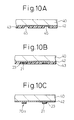
- FIG. 9 shows a variant of the pad for mounting a semiconductor element thereon
- FIGS. 10A to 10 C illustrate the formation of the pad shown in FIG. 9;
- FIGS. 11A and 11B illustrate disconnection of an electrode terminal of a semiconductor element from an pad of a mounting substrate, and connection of an electrode terminal of a semiconductor element with a pad of a mounting substrate through a surface layer of solder of the pad, respectively;
- FIGS. 12A to 12 G illustrate another method of manufacturing the multilayered substrate shown in FIG. 1;
- FIG. 13 shows a partial sectional view showing another embodiment of the multilayered substrate of the invention.
- FIGS. 14A to 14 D illustrate a method of manufacturing the multilayered substrate shown in FIG. 13;
- FIG. 15 shows an intermediate product for the multilayered substrate shown in FIG. 13;
- FIG. 16 is a partial sectional view showing a further embodiment of the multilayered substrate of the invention.
- FIG. 17 is a partial sectional view showing a multilayered substrate of the invention having incorporated therein a thin film capacitor
- FIGS. 18A and 18B illustrate a process for forming the thin film capacitor in the multilayered substrate shown in FIG. 17;
- FIG. 19 is a partial sectional view showing a conventional multilayered substrate.
- FIGS. 20A to 20 F illustrate a method of manufacturing the multilayered substrate shown in FIG. 19 .
- FIG. 1 illustrates a partial section of an embodiment of the substrate 10 of a multilayered structure of the invention.
- this multilayered substrate 10 a plurality of layers of wiring line 12 are present, and are separated from each other by an insulation layer 14 made of a resin, such as a polyimide or polyphenylene ether, interposed therebetween.
- the multilayered substrate 10 has one face in which pads 20 a to be bonded to an electrode terminals 18 of a semiconductor element 16 are provided, and another face on which pads 24 to be bonded to a solder ball 22 as an external connection terminal are provided. Both faces of the multilayered substrate 10 are covered by a layer of solder resist 26 except for the respective pads 20 a and 24 .
- a pad 20 which is used for the connection of a wiring line in one layer with a wiring line in another layer and can be formed as part of the wiring line of one of the layers, or the pad 20 a for the connection with a semiconductor element or the pad 24 for the connection with an external connection terminal, in one of the wiring line layers are electrically connected with another pad 20 , 20 a , or 24 of the adjacent wiring line layer through a via 28 piercing the insulation layer 14 interposed between the wiring line layers adjacent to each other.
- the substrate 10 of multilayered structure shown in FIG. 1 can be manufactured by a method illustrated in FIGS. 2 to 7 , in which wiring line layers and insulation layers are alternately formed successively from the side for mounting a semiconductor element thereon to the side to be bonded to external connection terminals, while wiring line layers on both sides of each insulation layer are connected with each other by vias piercing the insulation layer.
- a seed layer 42 is first formed on a surface of a copper sheet 40 as shown in FIG. 2 A. It is preferred that the surface of the copper sheet 40 on which the seed layer 42 is to be formed has an average surface roughness (Ra) of 0.1 micrometer or smaller. It is also preferred that if an average surface roughness (Ra) of a surface of a sheet of metal, such as copper as in this example, on which a seed layer is to be formed is in excess of 0.1 micrometer, the surface of the metal sheet is polished to have an average surface roughness (Ra) of 0.1 micrometer or smaller.
- the copper sheet 40 may be replaced with a sheet of aluminum or stainless steel.
- the seed layer 42 formed on the surface of the copper sheet 40 consists of a sublayer of chromium (Cr) 41 a directly in contact with the surface of the copper sheet 40 and having a thickness of, for example, 0.01 micrometer, and a sublayer of copper (Cu) 41 b formed on the sublayer of chromium 41 a and having a thickness of, for example, 0.1 micrometer.
- Cr chromium
- Cu copper
- the chromium sublayer 41 a is not etched by an etchant used later to etch the copper sheet 40 for its removal, as described below, and thus serves as an etching stopper layer during the etching of the copper sheet 40 .
- the copper sublayer 41 b serves as an electrical power supply layer during electrolytic plating described below.
- the chromium and copper sublayers 41 a and 41 b may be formed by sputtering, evaporation, or electroless plating.
- a sublayer of metal which may be etched by an etchant for the copper sheet 40 but has a noticeably slower etching rate than that of the copper sheet 40 , may be used.
- pads 20 a of copper are formed which have a thickness of about 10 micrometers, for example, the pad 20 a being subsequently bonded to an electrode terminal of a semiconductor element.
- These pads 20 a for the connection with a semiconductor element can be formed by forming a layer of photoresist (not shown) on the seed layer 42 , patterning the photoresist layer to expose portions of the seed layer 42 on which the pads 20 a are to be formed, and electrolytically plating the exposed portions with copper using the patterned photoresist layer as a mask and using the seed layer 42 , particularly the sublayer of copper 41 b , as an electrical power supply layer.
- a polyimide which is a thermosetting resin and has a thickness of about 30 micrometers, for example, is applied so as to cover the pads 20 a and the seed layer 42 of the copper sheet 40 , by printing or the like, and is cured to form an insulation layer 14 , as shown in FIG. 2 C.
- the insulation layer 14 is then pierced by a laser beam, such as YAG laser or carbon dioxide laser beam, to form holes 30 and expose part of the end face of the pads 20 a , as shown in FIG. 2 D.
- the hole thus formed has an opening at the surface of the insulation layer 14 , and the bottom defined by the exposed surface of the pad 20 a , the opening having a larger area than that of the bottom, in general, as exaggeratedly illustrated in the drawing.
- the holes 30 may be formed by etching the insulation layer 14 , or by forming an insulation layer 14 of photosensitive resin and patterning it by a photolithography process.
- a seed layer 42 ′ is formed to cover the entire surface of the insulation layer 14 , including the inside walls of the respective holes 30 , and the bottoms of the holes 30 (the exposed surfaces of the respective pads 20 a ), as shown in FIG. 2 E.
- This seed layer 42 ′ consists also of a sublayer of chromium (not shown for simplicity) in contact directly with the insulation layer 14 and the exposed pads 20 a and having a thickness of 0.01 micrometer, for example, and a sublayer of copper (also not shown for simplicity) formed on the sublayer of chromium and having a thickness of 0.1 micrometer, for example.
- the sublayer of chromium of the seed layer 42 ′ may be used, which can be formed by sputtering.
- the seed layer 42 ′ may be formed of thin layer of copper by electroless plating.
- a patterned photoresist layer 44 is formed on the seed layer 42 ′ to expose portions of the seed layer 42 ′ at which wiring lines and vias for the connection of the wiring line with the pad 20 a are to be formed, as illustrated in FIG. 4A.
- a layer of copper 46 is then formed at the exposed portions of the seed layer 42 ′ by electrolytic plating using the seed layer 42 ′ as an electrical power supply layer, to provide vias 28 , which consists of the plated copper layer 46 and the underlying seed layer 42 ′, and wiring lines having a thickness of the order of 10 micrometers, as illustrated in FIG. 4 B.
- the via 28 thus formed is a concave via in which the copper layer 46 having a certain thickness is formed along the inside wall of the hole 30 .
- the photoresist layer 44 is then removed, and the exposed seed layer 42 ′ is etched to removal, to leave vias 28 and wiring lines 12 on the surface of the insulation layer 14 , as illustrated in FIG. 2 F.
- the required number of sets of insulation and wiring line layers can be formed successively from the side for the mounting of a semiconductor element to the side for external connection terminals, to provide an intermediate product 10 a for a multilayered substrate, as shown in FIG. 5 .
- the intermediate product 10 a thus obtained has pads 20 a for the mounting of a semiconductor element at one side, which are covered by the copper sheet 40 through the interposed seed layer 42 , and pads 24 for the connection with an external connection terminal at the other side, which are formed as part of the formed wiring line.
- the copper sheet 40 can serve as a reinforcing sheet for the intermediate product 10 a , to facilitate the handling thereof, such as during transportation.
- the invention uses the sublayer of chromium 41 a of the seed layer 42 shown in FIG. 3, which is not etched by an etchant for copper sheet 40 , to prevent the pads 20 a for the mounting of semiconductor element from being etched by the etchant used to remove the copper sheet 40 .
- the etching of the copper sheet 40 is further described. It is very difficult to etch, at a uniform rate, the entire surface of the copper sheet 40 as shown in FIG. 6A and, accordingly, the etching of copper sheet 40 is prone to provide an uneven etched surface.
- the sublayer of chromium 41 a (FIG. 3) of the seed layer 42 which is not etched by an etchant for the copper sheet 40 , the etching is stopped, even at an area where the etching is locally accelerated, when the etching reaches the sublayer of chromium 41 a of the seed layer 42 .
- the etchant completely removes the copper sheet 40 , without removing or damaging the members of copper material, such as sublayer of copper 41 b (FIG. 3) and pads 20 a , underlying and protected by the sublayer of chromium 41 a (FIG. 3 ), as illustrated in FIG. 6 B.
- the seed layer 42 is then removed to expose the surface of the pad 20 a for the mounting of a semiconductor element, as shown in FIG. 6 C.
- the removal of the seed layer 42 is carried out by first etching the sublayer of chromium 41 a (FIG. 3) using an etchant which etches chromium and does not etch copper, and then etching the sublayer of copper 41 b (FIG. 3) using another etchant for copper.
- the sublayer of copper 41 b FIG.
- the etching raises no problem since the sublayer of copper 41 b has a thickness of the order of 0.1 micrometer whereas the pads 20 a have a much larger thickness of the order of 10 micrometers.
- a patterned solder resist layer is applied to each of the sides provided with the pads 20 a for the mounting of a semiconductor element and the side provided with pads 24 for external connection terminals, so as to expose both pads 20 a and 24 , to thereby provide the multilayered substrate 10 of the invention as illustrated in FIG. 1 .
- the multilayered substrate 10 can have a very flat surface which is formed of the pads 20 a and insulation layer 14 exposed by the successive removal of the copper sheet 40 and seed layer 42 , and the pad 20 a of the multilayered substrate 10 can be securely bonded to an electrode terminal 18 of a semiconductor element 16 (FIG. 1 ).
- the patterned photoresist layer 44 is formed on the seed layer 42 ′ by a photolithography process to expose portions of the seed layer 42 ′ at which wiring lines (not shown) and vias 28 are to be formed.
- This problem can be avoided by electrolytically plating the seed layer 42 ′ with a copper layer 47 using the seed layer 42 ′ as an electric power supply layer to thereby make the hole 30 shallower, as shown in FIG. 7A, so that the bottom of the hole 30 can receive a sufficient amount of light during exposure, and then forming a photoresist film to cover the copper layer 47 and fill the hole 30 .
- the photoresist film is then patterned to provide a patterned photoresist layer 44 , as shown in FIG. 7B, to expose portions of the copper layer 47 at which vias and wiring lines are to be formed. During this patterning, the photoresist filled in the hole 30 having a smaller depth is sufficiently photo-reacted, and can subsequently be completely removed.
- a patterned copper layer 46 having a certain thickness is formed to provide wiring lines (not shown) and concave vias 28 having a smaller depth.
- the photoresist layer 44 is then removed, and the exposed copper layer 47 and the underlying seed layer 42 ′ are also removed, to leave vias 28 , which consist of the seed layer 42 ′ and the patterned copper layers 47 and 46 , and wiring lines 12 on the surface of the insulation layer 14 , as illustrated in FIG. 2 F.
- vias having a still smaller diameter they may be formed by the following method, which is described by making reference to FIGS. 8A to 8 C.
- a thin film layer of copper 54 is formed to cover the insulation layer 14 and the exposed surfaces of the pads 20 a , as shown in FIG. 8 A.
- the thin film layer of copper 54 may be formed by sputtering, electroless plating or the like.
- a layer of chromium or titanium (not shown) may be formed on the insulation layer 14 by sputtering or electroless plating, the layer of chromium or titanium representing the sublayer 41 a of the seed layer 42 referred to above.
- a copper layer 56 is then formed on the thin film layer of copper 54 to have a thickness which enables the holes 30 to be completely filled with the copper material, as illustrated in FIG. 8 B.
- the copper layer 56 thus formed has small recesses 55 at locations corresponding to the locations of the respective holes 30 , the smaller the diameter of the via to be formed is, the smaller the diameter of the hole 30 is, and also the smaller the recess 55 appearing at the surface of the copper layer 56 is, resulting in the formation of copper layer 56 having an almost flat, or even substantially flat, surface.
- the copper layers 56 and 54 are patterned to provide vias 28 and wiring lines 12 , as illustrated in FIG. 8 C.
- the pads 20 a for the mounting of a semiconductor element are made up only of a layer of copper, they may be made up of two or more layers of different metals.
- FIG. 9 shows an example in which the pads 20 a for the mounting of a semiconductor element is made up of a layer of copper 21 and a layer of gold 23 .
- the layer of gold 23 forms a surface layer of the pad 20 a for the mounting of a semiconductor element, and serves as an surface protective layer for protecting the copper layer 21 from oxidation and the like.
- the surface gold layer may also be combined with an underlying nickel layer or underlying palladium and nickel layers to form a laminated structure of gold (Au)-nickel (Ni) or gold (Au)-palladium (Pd)-nickel (Ni).
- the pads 20 a for the mounting of a semiconductor element shown in FIG. 9 may be formed as illustrated in FIGS. 10A to 10 C.
- a resin layer 43 is first formed on a seed layer 42 provided on a copper sheet 40 , the seed layer 42 consisting also of sublayers 41 a and 41 b as illustrated in FIG. 3, and holes 45 for the formation of pads 20 a is then formed in the resin layer 43 by use of a laser beam or etching, as shown in FIG. 10A.
- a layer of gold 23 is formed on the seed layer 42 by electrolytic plating using the seed layer 42 as an electric power supply layer, and a copper layer 21 is then formed on the gold layer 23 by also electrolytic plating, as illustrated in FIG. 10 B.
- the resin layer 43 is removed to provide pads 20 a of two-layer structure for the mounting of a semiconductor element, as illustrated in FIG. 10 C.
- a multilayered substrate can be obtained using any process referred to above.
- the gold layer 23 of the pad 20 a for the mounting of a semiconductor element shown in FIG. 9 may be substituted with a layer of solder 25 .
- the solder used in the layer 25 is a metallic material having a low melting temperature which is melted under a heating atmosphere of a subsequent step of reflowing another solder material, such as a solder ball, used for mounting a semiconductor element on the multilayered substrate, the melted solder material being capable of electrically connecting the pads 20 a with an electrode terminal of a semiconductor element to be mounted.
- solder material forming the solder layer 25 any material which is melted under an heating atmosphere of the reflowing step can be used, with an alloy free of lead, such as a tin (Sn)-silver (Ag) alloy, being preferred.
- some of electrode terminals 18 of a semiconductor element 16 may be disconnected from a pad 20 a of a multilayered substrate on which the semiconductor element 16 is mounted, as illustrated in FIG. 11 A.
- a solder layer 25 is provided at the surface of a pad 20 a , as described above, such a problem of disconnection of a pad 20 a and an electrode terminal 18 of a semiconductor element 16 may be avoided, because the solder layer 25 is melted into a molten solder having an elliptic section due to its surface tension under a heating atmosphere of a reflow process, and part of the molten solder of elliptic section projects over the surface of the insulation layer 14 to be in contact with the electrode terminal 18 of the semiconductor element 16 , to thereby electrically connect the pad 20 a of the multilayered substrate with the electrode terminal 18 of the semiconductor element 16 , as illustrated in FIG.
- solder layer 25 For the solder layer 25 to be transformed into a molten solder having an elliptic section useful to reliably connect the pad 20 a with the electrode terminal 18 of the semiconductor element 16 , it is preferred that a solder material for the surface layer 25 of the pad 20 a has a lower melting point, for example, 270 to 280° C., than that of a solder material for the electrode terminal 18 of the semiconductor element 16 , which has, in general, a melting point of the order of 320° C.
- a solder material for the surface layer 25 of the pad 20 a has a lower melting point, for example, 270 to 280° C., than that of a solder material for the electrode terminal 18 of the semiconductor element 16 , which has, in general, a melting point of the order of 320° C.
- the solder layer provided at the surface of the pad 20 a can be formed similarly to the formation of the gold layer 23 illustrated in FIG. 10 .
- the seed layer 42 is formed on one side of the copper sheet 40 .
- the pad 20 a for the mounting of a semiconductor element has a surface layer of gold 23 , as shown in FIG. 9, the layer of gold 23 is not etched by an etchant for the copper sheet 40 during its removal and, consequently, the formation of the seed layer 42 (FIG. 2 A and FIG. 3) is unnecessary.
- the solder layer is etched by an etchant for the copper sheet 40 during its removal.
- the solder material has a noticeably slower etching rate than that of the copper sheet, and is substantially not etched, and, consequently, the formation of the seed layer 42 (FIG. 2 A and FIG. 3) is also unnecessary.
- a multilayered substrate can be produced omitting the seed layer 42 (FIG. 2 A and FIG. 3) in order to shorten a production process of the multilayered substrate.
- a method of producing a multilayered substrate of the invention without using the seed layer 42 on the copper sheet 40 will be described, making reference to FIGS. 12A to 12 G.
- the following description is directed to the manufacture of a multilayered substrate having pads 20 a formed of gold and copper layers 23 and 21 , although the method described below may also be applied to the manufacture of a multilayered substrate having pads 20 a having a surface of solder or copper.
- a resin film 43 is first formed on a surface of a copper sheet 40 . It is preferred that a surface on which the resin film 43 is formed has an average surface roughness (Ra) of 0.1 micrometer of smaller, as in the embodiment illustrated in FIG. 2 . If an average roughness (Ra) of the surface of the copper sheet 40 , on which the resin film 43 is formed, is in excess of 0.1 micrometer, it is preferred that the surface is polished to have an average surface roughness (Ra) of 0.1 micrometer or smaller.
- the resin film 43 is formed of a resin which is not etched by an etchant for the copper sheet 40 , or a resin which is substantially not etched by the etchant, such as an epoxy, polyimide, polyphenylene ether or the like.
- Holes 45 for the formation of pads for the mounting of a semiconductor element are then formed in the resin film 43 by use of a laser beam or etching, as shown in FIG. 12 B. Subsequently, a layer of gold 23 is formed in the hole 45 so as to be in contact with the copper sheet 40 by electrolytic plating using the copper sheet 40 as an electric power supply layer, and a copper layer 21 is successively formed on the gold layer 23 by electrolytic plating, to form a pad 20 a of two-layer structure for the mounting of a semiconductor element, as illustrated in FIG. 12 C.
- a resin film 48 is then formed so as to cover the pads 20 a , as shown in FIG. 12 D.
- the resin film 48 is formed of the same resin as the resin forming the film 43 on the copper sheet 40 , and the resin films 43 and 48 are integrated into an insulation layer 49 , as illustrated in the drawing.
- Holes 30 are then formed in the insulation layer 49 by a beam of a laser, such as YAG or carbon dioxide laser, as shown in FIG. 12 E.
- the hole thus formed has an opening at the surface of the insulation layer 49 , and the bottom defined by the exposed surface of the pad 20 a , the opening having a larger area or diameter than that of the bottom, in general, as exaggeratedly illustrated in FIG. 12 E.
- the hole 30 may be formed by etching the insulation layer 49 , or by forming an insulation layer 49 of photosensitive resin and patterning it by a photolithography process.
- a thin film layer of copper 50 is formed to cover the entire surface of the insulation layer 49 , including the inside walls of the holes 30 , and the exposed surfaces of the pads 20 a , as shown in FIG. 12F, by electroless plating, sputtering, evaporation or the like.
- the thin film layer of copper 50 on the inside wall of the hole 30 has a thickness of about 0.1 micrometer, for example.
- a photoresist layer (not shown) is then formed on the thin film layer of copper 50 , and is patterned to expose portions of the copper layer 50 at which vias and wiring lines are to be formed. This step of the formation and patterning of photoresist layer is similar to that already described making reference to FIG. 4 A.
- a layer of copper (not shown) is then formed at the exposed portions of the thin film layer of copper 50 by electrolytic plating, using the thin film layer of copper 50 as an electrical power supply layer, to provide vias 28 (FIG. 12G) and wiring lines 12 (FIG. 12G) having a thickness of the order of 10 micrometers.
- the via 28 thus formed is a concave via in which the copper layer having a certain thickness is formed along the inside wall of the hole 30 .
- the photoresist layer is then removed, and the exposed thin film layer of copper 50 is etched to removal, to leave vias 28 and wiring lines 12 on the surface of the insulation layer 49 , as illustrated in FIG. 12 G.
- the via 28 in each of layers of the multilayered substrate is generally a concave via in which a metallic layer having a certain thickness is formed along the inside wall of a hole for the formation of the via, and a further layer is formed on the layer having an uneven configuration resulting from the concave vias therein. Accordingly, a finally produced multilayered substrate tends to have a surface, for external connection terminals, which is more or less uneven. Such unevenness in the surface of multilayered substrate to be provided with external connection terminals may be absorbed when external connection terminals are bonded to the substrate, because solder balls as the external connection terminals are larger than electrode terminals of a semiconductor element to be mounted on the multilayered substrate. With a solder ball having a smaller size, however, pads for external connection terminals of the multilayered substrate is required to be arranged in the same or substantially the same plane.
- FIG. 13 shows a multilayered substrate 50 having pads for external connection terminals which are in the same or substantially the same plane to satisfy such a requirement.
- members of the multilayered substrate 50 which are the same as those of the multilayered substrate 10 illustrated in FIG. 1, are indicated by the same reference numerals as in FIG. 1, and are not described hereinafter in detail.
- the multilayered substrate 50 shown in FIG. 13 is different from the multilayered substrate 10 shown in FIG. 1 in that, in the former, vias 52 are columns of copper, i.e., solid bodies formed of copper material filled in holes 30 of an insulation layer 14 , and the end faces of the vias 52 formed in an insulation layer 14 are arranged in the same plane.
- the multilayered substrate 50 shown in FIG. 13 may be produced by a method illustrated in FIGS. 14A to 14 D.
- the steps illustrated in FIGS. 2A to 2 D are also employed to form holes 30 for the formation of via in the insulation layer 14 .
- the hole 30 has an opening at the surface of the insulation layer 14 , and the bottom defined by the exposed surface of the pad 20 a , the opening having a larger area than that of the bottom, in general, as exaggeratedly illustrated in FIG. 2 D.
- a thin film layer of copper 54 is formed on the surface of the insulation layer 14 , including the inside walls of the holes 30 , and the exposed surfaces of the pads 20 a (the bottoms of the holes 30 ), by sputtering or the like, as shown in FIG. 14A.
- a further layer of copper (not shown) is then formed on the thin film layer of copper 54 by electrolytic plating using the thin film layer of copper 54 as an electric power supply layer, the plated layer of copper having a thickness enabling the hole 30 to be filled with the copper material, and is integrated with the thin film layer of copper 54 into an integrated copper layer 56 , as shown in FIG. 14 B.
- the integrated copper layer 56 thus formed has recesses 55 at the locations corresponding to the locations of the holes 30 .
- the copper layer 56 on the insulation layer 14 is then abraded to be removed and leave vias 52 , which are made up of the copper material filled in the holes 30 .
- vias 52 are made up of the copper material filled in the holes 30 .
- the surface of the insulation layer 14 and the end faces of the vias 52 are positioned in the same plane, as illustrated in FIG. 14 C.
- a copper layer (not shown) is then formed to cover the insulation layer 14 and the end faces of the vias 52 by electroless plating, electrolytic plating, sputtering or the like, and is patterned by a photolithography process or the like to form a wiring line layer including pads 20 and wiring lines 12 , as shown in FIG. 14 D.
- the intermediate product 50 a thus obtained has the copper sheet 40 bonded to its surface, on which a semiconductor element is to be mounted, through a seed layer 42 , as in the intermediate product 10 a shown in FIG. 5 .
- the copper sheet 40 can serve as a reinforcing sheet for the intermediate product 50 a , and facilitate handling, such as during transportation, of the intermediate product 50 a.
- etching of the copper sheet 40 is carried out by use of an etchant for copper material and, when the etching reaches the sublayer of chromium 41 a (FIG. 3) forming the seed layer 42 , the etching is terminated. Subsequently, the sublayer of chromium 41 a is removed using an etchant which etches chromium and does not etch copper, and the sublayer of copper 41 b (FIG. 3) also forming the seed layer 42 is then removed by an etchant for copper.
- a patterned solder resist layer 26 is formed on each of the sides of the remaining laminate of sets of the insulation layers 14 and the wiring line layers so as to expose pads 20 a for the mounting of a semiconductor element and the pads 24 for external connection terminals, to provide the multilayered substrate 50 shown in FIG. 13, which has pads 24 for external connection terminals arranged in the same plane, and is particularly suitable for external connection terminals made up of smaller solder balls.
- part of the copper sheet 40 used in the production of the multilayered substrates 10 and 50 described above is completely removed after finishing the production, part of the copper sheet 40 may be left along a peripheral region of the product multilayered substrate 10 (or 50 ) to form a frame member 41 , as shown in FIG. 16 .
- a technique such as photolithography may be employed.
- FIG. 16 shows only the frame member on the multilayered substrate 10 having concave vias 28 , a person with ordinary skill in the art can easily understand that a similar frame member can be provided on the multilayered substrate 50 having solid vias.
- the frame member 41 is securely bonded to the multilayered substrate 10 (or 50 ) through the seed layer 42 , and can serve as a stiffener for the multilayered substrate 10 (or 50 ) to improve its handleability during transportation and the like.
- a thin film capacitor by interposing a film of dielectric having a high dielectric constant (not shown) between the frame member 41 and the seed layer 42 .
- a thin film capacitor 51 in a multilayered substrate 50 ′ as illustrated in FIG. 17 .
- the multilayered substrate 50 ′ represents the multilayered substrate 50 having the solid vias 52 as described making reference to FIG. 13 .
- the thin film capacitor 51 is formed immediately adjacent to an electrode terminal 18 of a semiconductor element 16 to be mounted on the substrate 50 ′.
- the thin film capacitor 51 incorporated in the multilayered substrate 50 ′ shown in FIG. 17 is formed on the seed layer 42 provided on the surface of the copper sheet 40 , as illustrated in FIG. 18 A.
- a pad 20 a for the mounting of a semiconductor element is first formed on the seed layer 42 by sputtering.
- a layer of dielectric 53 having a high dielectric constant, such as strontium titanate (SrTiO 3 ), barium titanate (BaTiO 3 ) or the like, and a thickness of, for example, 1 micrometer is then formed on the pad 20 a by sputtering.
- a thin film layer of copper 57 having a thickness of, for example, 20 micrometers is then formed on the layer of dielectric 53 to produce the thin film capacitor 51 .
- an intermediate product 50 a′ which is similar to the intermediate product 50 a illustrated in FIG. 15 and has the incorporated capacitor 51 can be obtained, which can also be further processed to produce the product multilayered substrate 50 ′ illustrated in FIG. 17 .
- the copper sheet 40 is used for the production of the multilayered substrate.
- This copper sheet 40 may be replaced with a metallic sheet made of aluminum or stainless steel, for example.
- a seed layer 42 may also be formed between the pads 20 a for the mounting of a semiconductor element and the metallic sheet to improve adhesion therebetween.
- the pads 20 a for the mounting of a semiconductor element is formed of copper, and the metallic sheet is formed of aluminum, the metallic sheet can be etched without etching the pads 20 a of copper by selecting an appropriate etchant, making the seed layer 42 unnecessary.
- a metallic frame member 17 having a required strength may additionally be provided at a peripheral region of a multilayered substrate 10 , as illustrated in FIG. 1 .
- a multilayered substrate can have a surface for the mounting of a semiconductor element, which is flat or substantially flat, to thereby securely connect electrode terminals of the semiconductor element with the pads of the multilayered substrate. Further, the invention can make unnecessary a core substrate which is essential for the production of a conventional multilayered substrate, and can provide a thinner multilayered substrate.
Landscapes
- Engineering & Computer Science (AREA)
- Microelectronics & Electronic Packaging (AREA)
- Physics & Mathematics (AREA)
- Condensed Matter Physics & Semiconductors (AREA)
- General Physics & Mathematics (AREA)
- Computer Hardware Design (AREA)
- Power Engineering (AREA)
- Manufacturing & Machinery (AREA)
- Production Of Multi-Layered Print Wiring Board (AREA)
Abstract
Description
Claims (21)
Priority Applications (3)
| Application Number | Priority Date | Filing Date | Title |
|---|---|---|---|
| US09/815,047 US6441314B2 (en) | 1999-03-11 | 2001-03-23 | Multilayered substrate for semiconductor device |
| US10/207,259 US6931724B2 (en) | 1999-03-11 | 2002-07-30 | Insulated multilayered substrate having connecting leads for mounting a semiconductor element thereon |
| US10/920,270 US7763809B2 (en) | 1999-03-11 | 2004-08-18 | Multilayered substrate for semiconductor device and method of manufacturing same |
Applications Claiming Priority (4)
| Application Number | Priority Date | Filing Date | Title |
|---|---|---|---|
| JP11-064248 | 1999-03-11 | ||
| JP6424899 | 1999-03-11 | ||
| JP11-370984 | 1999-12-27 | ||
| JP37098499A JP3635219B2 (en) | 1999-03-11 | 1999-12-27 | Multilayer substrate for semiconductor device and manufacturing method thereof |
Related Child Applications (1)
| Application Number | Title | Priority Date | Filing Date |
|---|---|---|---|
| US09/815,047 Division US6441314B2 (en) | 1999-03-11 | 2001-03-23 | Multilayered substrate for semiconductor device |
Publications (1)
| Publication Number | Publication Date |
|---|---|
| US6418615B1 true US6418615B1 (en) | 2002-07-16 |
Family
ID=26405372
Family Applications (4)
| Application Number | Title | Priority Date | Filing Date |
|---|---|---|---|
| US09/523,149 Expired - Lifetime US6418615B1 (en) | 1999-03-11 | 2000-03-10 | Method of making multilayered substrate for semiconductor device |
| US09/815,047 Expired - Lifetime US6441314B2 (en) | 1999-03-11 | 2001-03-23 | Multilayered substrate for semiconductor device |
| US10/207,259 Expired - Lifetime US6931724B2 (en) | 1999-03-11 | 2002-07-30 | Insulated multilayered substrate having connecting leads for mounting a semiconductor element thereon |
| US10/920,270 Expired - Lifetime US7763809B2 (en) | 1999-03-11 | 2004-08-18 | Multilayered substrate for semiconductor device and method of manufacturing same |
Family Applications After (3)
| Application Number | Title | Priority Date | Filing Date |
|---|---|---|---|
| US09/815,047 Expired - Lifetime US6441314B2 (en) | 1999-03-11 | 2001-03-23 | Multilayered substrate for semiconductor device |
| US10/207,259 Expired - Lifetime US6931724B2 (en) | 1999-03-11 | 2002-07-30 | Insulated multilayered substrate having connecting leads for mounting a semiconductor element thereon |
| US10/920,270 Expired - Lifetime US7763809B2 (en) | 1999-03-11 | 2004-08-18 | Multilayered substrate for semiconductor device and method of manufacturing same |
Country Status (2)
| Country | Link |
|---|---|
| US (4) | US6418615B1 (en) |
| JP (1) | JP3635219B2 (en) |
Cited By (69)
| Publication number | Priority date | Publication date | Assignee | Title |
|---|---|---|---|---|
| US20020170173A1 (en) * | 2001-05-21 | 2002-11-21 | Shinko Electric Industries Co., Ltd. | Method of production of circuit board, semiconductor device, and plating system |
| US6591495B2 (en) * | 1998-09-03 | 2003-07-15 | Ibiden Co., Ltd. | Manufacturing method of a multilayered printed circuit board having an opening made by a laser, and using electroless and electrolytic plating |
| US20030178388A1 (en) * | 2002-03-22 | 2003-09-25 | Phillips Kenneth L. | Inverted micro-vias |
| US20040004288A1 (en) * | 2000-08-24 | 2004-01-08 | Matsushita Electric Industrial Co., Ltd. | Semiconductor device and manufacturing method of the same |
| US20040012930A1 (en) * | 2002-02-12 | 2004-01-22 | Grigg Ford B. | Microelectronic devices and methods for mounting microelectronic packages to circuit boards |
| US20040046244A1 (en) * | 2001-10-31 | 2004-03-11 | Shinko Electric Industries Co., Ltd. | Multilayered substrate for semiconductor device |
| US20040060174A1 (en) * | 2002-09-17 | 2004-04-01 | Shinko Electric Industries Co. Ltd. | Method for producing wiring substrate |
| US6717070B2 (en) * | 2000-07-07 | 2004-04-06 | Kabushiki Kaisha Toshiba | Printed wiring board having via and method of manufacturing the same |
| US20040074088A1 (en) * | 2001-10-31 | 2004-04-22 | Jyunichi Nakamura | Method for manufacturing multilayer circuit board for semiconductor device |
| US20040079643A1 (en) * | 2002-10-29 | 2004-04-29 | Noritaka Ban | Method for manufacturing wiring substrates |
| US6841862B2 (en) | 2000-06-30 | 2005-01-11 | Nec Corporation | Semiconductor package board using a metal base |
| US20050006744A1 (en) * | 2003-05-30 | 2005-01-13 | Shinko Electric Industries Co., Ltd. | Package for semiconductor devices |
| US20050041398A1 (en) * | 2002-05-01 | 2005-02-24 | Huemoeller Ronald Patrick | Integrated circuit substrate having embedded back-side access conductors and vias |
| US20050133256A1 (en) * | 2003-12-19 | 2005-06-23 | Brother Kogyo Kabushiki Kaisha | Method for manufacturing a printed circuit board that mounts an integrated circuit device thereon and the printed circuit board |
| US20050155222A1 (en) * | 2004-01-19 | 2005-07-21 | Shinko Electric Industries Co., Ltd. | Circuit substrate manufacturing method |
| US20050252682A1 (en) * | 2004-05-12 | 2005-11-17 | Nec Corporation | Wiring board and semiconductor package using the same |
| US7019404B2 (en) | 2002-01-24 | 2006-03-28 | Shinko Electric Industries Co., Ltd. | Multilayered circuit substrate, semiconductor device and method of producing same |
| US20060125042A1 (en) * | 2003-07-28 | 2006-06-15 | Edward Fuergut | Electronic component and panel for producing the same |
| US20060124351A1 (en) * | 2002-01-15 | 2006-06-15 | Sony Corporation | Flexible multilayer wiring board and manufacture method thereof |
| US20060283625A1 (en) * | 2005-06-17 | 2006-12-21 | Nec Corporation | Wiring board, method for manufacturing same, and semiconductor package |
| US20070084630A1 (en) * | 2005-10-14 | 2007-04-19 | Samsung Electro-Mechanics Co., Ltd. | Coreless substrate and manufacturing method thereof |
| US20070193679A1 (en) * | 2005-12-21 | 2007-08-23 | Ibiden Co., Ltd. | Printed wiring board manufacturing method |
| US20070246253A1 (en) * | 2004-07-06 | 2007-10-25 | Masami Yakabe | Through Substrate, Interposer and Manufacturing Method of Through Substrate |
| US20080043447A1 (en) * | 2002-05-01 | 2008-02-21 | Amkor Technology, Inc. | Semiconductor package having laser-embedded terminals |
| US20080258300A1 (en) * | 2007-04-13 | 2008-10-23 | Shinko Electric Industries Co., Ltd. | Wiring board manufacturing method, semiconductor device manufacturing method and wiring board |
| US20090052150A1 (en) * | 2007-08-24 | 2009-02-26 | Shinko Electric Industries Co,, Ltd. | Wiring board, method of manufacturing the same, and semiconductor device having wiring board |
| US20090084494A1 (en) * | 2007-09-28 | 2009-04-02 | Samsung Electro-Mechanics Co., Ltd. | Substrate manufacturing method |
| US20090141464A1 (en) * | 2007-11-29 | 2009-06-04 | Shinko Electric Industries Co., Ltd. | Wiring board and electronic component device |
| US20090140442A1 (en) * | 2007-12-03 | 2009-06-04 | Stats Chippac, Ltd. | Wafer Level Package Integration and Method |
| US20090145636A1 (en) * | 2007-12-05 | 2009-06-11 | Shinko Electric Industries Co., Ltd. | Electronic component mounting package |
| US20090181496A1 (en) * | 2007-06-20 | 2009-07-16 | Princo Corp. | Multi-layer substrate and manufacture method thereof |
| US20090229874A1 (en) * | 2008-03-13 | 2009-09-17 | Hiroshi Katagiri | Multilayer wiring board |
| US20090236138A1 (en) * | 2008-03-13 | 2009-09-24 | Hiroshi Katagiri | Multilayer wiring board and method of manufacturing the same |
| US7670962B2 (en) | 2002-05-01 | 2010-03-02 | Amkor Technology, Inc. | Substrate having stiffener fabrication method |
| US20100065959A1 (en) * | 2008-09-18 | 2010-03-18 | Shinko Electric Industries Co., Ltd. | Semiconductor package and method of manufacturing the same, and semiconductor device |
| US7752752B1 (en) | 2007-01-09 | 2010-07-13 | Amkor Technology, Inc. | Method of fabricating an embedded circuit pattern |
| US20100175915A1 (en) * | 2009-01-09 | 2010-07-15 | Samsung Electro-Mechanics Co., Ltd. | Printed circuit board and method of manufacturing the same |
| US20100175917A1 (en) * | 2009-01-15 | 2010-07-15 | Shinko Electric Industries Co., Ltd. | Wiring board and method of manufacturing the same |
| CN101106121B (en) * | 2006-07-14 | 2010-12-08 | 恩益禧电子股份有限公司 | Wiring substrate, semiconductor device, and method of manufacturing the same |
| US20110010932A1 (en) * | 2007-11-22 | 2011-01-20 | Shinko Electric Industries Co., Ltd. | Wiring board, semiconductor device having wiring board, and method of manufacturing wiring board |
| US7902660B1 (en) * | 2006-05-24 | 2011-03-08 | Amkor Technology, Inc. | Substrate for semiconductor device and manufacturing method thereof |
| US7911037B1 (en) | 2006-10-04 | 2011-03-22 | Amkor Technology, Inc. | Method and structure for creating embedded metal features |
| US7932595B1 (en) | 2002-11-08 | 2011-04-26 | Amkor Technology, Inc. | Electronic component package comprising fan-out traces |
| US20110147934A1 (en) * | 2007-06-12 | 2011-06-23 | Texas Instruments Incorporated | Metal Plugged Substrates with No Adhesive Between Metal and Polyimide |
| US7977163B1 (en) | 2005-12-08 | 2011-07-12 | Amkor Technology, Inc. | Embedded electronic component package fabrication method |
| US7985663B2 (en) | 2008-05-27 | 2011-07-26 | Kabushiki Kaisha Toshiba | Method for manufacturing a semiconductor device |
| US20110233786A1 (en) * | 2010-03-24 | 2011-09-29 | Soichi Homma | Semiconductor device and method for manufacturing the same |
| US20110254156A1 (en) * | 2007-12-03 | 2011-10-20 | Stats Chippac, Ltd. | Semiconductor Device and Method of Wafer Level Package Integration |
| US20110296681A1 (en) * | 2007-09-20 | 2011-12-08 | Ibiden Co., Ltd | Printed wiring board and method for manufacturing same |
| US8188584B1 (en) | 2002-11-08 | 2012-05-29 | Amkor Technology, Inc. | Direct-write wafer level chip scale package |
| US8316536B1 (en) | 2002-05-01 | 2012-11-27 | Amkor Technology, Inc. | Multi-level circuit substrate fabrication method |
| US20130097856A1 (en) * | 2007-05-30 | 2013-04-25 | Shinko Electric Industries Co., Ltd. | Method of fabricating a wiring board |
| US20130134127A1 (en) * | 2008-10-03 | 2013-05-30 | Shinko Electric Industries Co., Ltd. | Wiring board and method of fabricating the same |
| US8525317B1 (en) * | 2001-09-27 | 2013-09-03 | Marvell International Ltd. | Integrated chip package having intermediate substrate with capacitor |
| US20130264716A1 (en) * | 2007-12-26 | 2013-10-10 | Stats Chippac, Ltd. | System-In-Package Having Integrated Passive Devices and Method Therefor |
| US20140210081A1 (en) * | 2013-01-29 | 2014-07-31 | Taiwan Semiconductor Manufacturing Company, Ltd. | Packaging Methods and Packaged Semiconductor Devices |
| US8802504B1 (en) * | 2013-03-14 | 2014-08-12 | Taiwan Semiconductor Manufacturing Company, Ltd. | 3D packages and methods for forming the same |
| US8826531B1 (en) | 2005-04-05 | 2014-09-09 | Amkor Technology, Inc. | Method for making an integrated circuit substrate having laminated laser-embedded circuit layers |
| US8872329B1 (en) | 2009-01-09 | 2014-10-28 | Amkor Technology, Inc. | Extended landing pad substrate package structure and method |
| US8959758B2 (en) | 2011-03-26 | 2015-02-24 | Fujitsu Limited | Method of manufacturing circuit board, method of manufacturing electronic device, and electronic device |
| US20150282314A1 (en) * | 2014-03-31 | 2015-10-01 | Ibiden Co., Ltd. | Method for manufacturing printed wiring board with conductive post and printed wiring board with conductive post |
| US9299649B2 (en) | 2013-02-08 | 2016-03-29 | Taiwan Semiconductor Manufacturing Company, Ltd. | 3D packages and methods for forming the same |
| US20160135326A1 (en) * | 2014-11-12 | 2016-05-12 | Samsung Electronics Co., Ltd. | Printed circuit board and semiconductor package |
| US9693455B1 (en) * | 2014-03-27 | 2017-06-27 | STATS ChipPAC Pte. Ltd. | Integrated circuit packaging system with plated copper posts and method of manufacture thereof |
| US9812386B1 (en) | 2002-05-01 | 2017-11-07 | Amkor Technology, Inc. | Encapsulated semiconductor package |
| US10811277B2 (en) | 2004-03-23 | 2020-10-20 | Amkor Technology, Inc. | Encapsulated semiconductor package |
| US20210118787A1 (en) * | 2019-10-18 | 2021-04-22 | Taiwan Semiconductor Manufacturing Company, Ltd. | Hybrid Dielectric Scheme in Packages |
| US11081370B2 (en) | 2004-03-23 | 2021-08-03 | Amkor Technology Singapore Holding Pte. Ltd. | Methods of manufacturing an encapsulated semiconductor device |
| US11094560B1 (en) | 2004-03-23 | 2021-08-17 | Amkor Technology Singapore Holding Pte. Ltd. | Encapsulated semiconductor package |
Families Citing this family (100)
| Publication number | Priority date | Publication date | Assignee | Title |
|---|---|---|---|---|
| US6884944B1 (en) * | 1998-01-14 | 2005-04-26 | Mitsui Mining & Smelting Co., Ltd. | Multi-layer printed wiring boards having blind vias |
| JP3635219B2 (en) * | 1999-03-11 | 2005-04-06 | 新光電気工業株式会社 | Multilayer substrate for semiconductor device and manufacturing method thereof |
| KR100556818B1 (en) * | 1999-05-13 | 2006-03-10 | 이비덴 가부시키가이샤 | Multilayer printed-circuit board and method of manufacture |
| GB2385465A (en) * | 1999-11-04 | 2003-08-20 | Nec Corp | Flip-chip stress aborbing layers and connections |
| JP3450238B2 (en) * | 1999-11-04 | 2003-09-22 | Necエレクトロニクス株式会社 | Semiconductor device and manufacturing method thereof |
| JP3838232B2 (en) * | 2000-06-30 | 2006-10-25 | 日本電気株式会社 | Semiconductor package substrate manufacturing method and semiconductor device manufacturing method |
| JP4905749B2 (en) * | 2001-03-02 | 2012-03-28 | 日立化成工業株式会社 | WIRING BOARD, ITS MANUFACTURING METHOD, SEMICONDUCTOR MOUNTING BOARD USING THE WIRING BOARD, ITS MANUFACTURING METHOD, SEMICONDUCTOR PACKAGE AND ITS MANUFACTURING METHOD |
| EP1773105B1 (en) * | 2001-03-14 | 2009-05-27 | Ibiden Co., Ltd. | Multilayer printed circuit board |
| JP2003023250A (en) * | 2001-07-06 | 2003-01-24 | Denso Corp | Multilayered substrate and its manufacturing method |
| US6847527B2 (en) * | 2001-08-24 | 2005-01-25 | 3M Innovative Properties Company | Interconnect module with reduced power distribution impedance |
| US6861757B2 (en) | 2001-09-03 | 2005-03-01 | Nec Corporation | Interconnecting substrate for carrying semiconductor device, method of producing thereof and package of semiconductor device |
| US20030066679A1 (en) * | 2001-10-09 | 2003-04-10 | Castro Abram M. | Electrical circuit and method of formation |
| JP3492348B2 (en) * | 2001-12-26 | 2004-02-03 | 新光電気工業株式会社 | Method of manufacturing package for semiconductor device |
| US7474538B2 (en) | 2002-05-27 | 2009-01-06 | Nec Corporation | Semiconductor device mounting board, method of manufacturing the same, method of inspecting the same, and semiconductor package |
| JP3591524B2 (en) * | 2002-05-27 | 2004-11-24 | 日本電気株式会社 | Semiconductor device mounting board, method of manufacturing the same, board inspection method thereof, and semiconductor package |
| US7084354B2 (en) * | 2002-06-14 | 2006-08-01 | Intel Corporation | PCB method and apparatus for producing landless interconnects |
| JP2004111544A (en) * | 2002-09-17 | 2004-04-08 | Ngk Spark Plug Co Ltd | Multilayer wiring board |
| JP3983146B2 (en) | 2002-09-17 | 2007-09-26 | Necエレクトロニクス株式会社 | Manufacturing method of multilayer wiring board |
| JP3910907B2 (en) | 2002-10-29 | 2007-04-25 | 新光電気工業株式会社 | Capacitor element and manufacturing method thereof, substrate for semiconductor device, and semiconductor device |
| JP2004186265A (en) * | 2002-11-29 | 2004-07-02 | Ngk Spark Plug Co Ltd | Method for manufacturing multilayer wiring board |
| JP4267903B2 (en) * | 2002-11-29 | 2009-05-27 | 日本特殊陶業株式会社 | Manufacturing method of multilayer wiring board |
| KR20070097598A (en) * | 2002-12-13 | 2007-10-04 | 가부시키가이샤 가네카 | Thermoplastic polyimide resin film, multilayer body and method for manufacturing printed wiring board composed of same |
| US6806563B2 (en) * | 2003-03-20 | 2004-10-19 | International Business Machines Corporation | Composite capacitor and stiffener for chip carrier |
| US7265300B2 (en) | 2003-03-21 | 2007-09-04 | Commscope Solutions Properties, Llc | Next high frequency improvement using hybrid substrates of two materials with different dielectric constant frequency slopes |
| TWI221667B (en) * | 2003-05-29 | 2004-10-01 | Advanced Semiconductor Eng | Substrate and process for fabricating the same |
| JP2005039243A (en) * | 2003-06-24 | 2005-02-10 | Ngk Spark Plug Co Ltd | Intermediate substrate |
| JP2005026316A (en) * | 2003-06-30 | 2005-01-27 | Tohoku Pioneer Corp | Printed circuit board and electronic apparatus |
| US20050121769A1 (en) * | 2003-12-05 | 2005-06-09 | Watts Nicholas R. | Stacked integrated circuit packages and methods of making the packages |
| JP3855992B2 (en) * | 2003-12-17 | 2006-12-13 | セイコーエプソン株式会社 | Semiconductor device and manufacturing method thereof, circuit board, and electronic apparatus |
| JP4549693B2 (en) * | 2004-02-27 | 2010-09-22 | 日本特殊陶業株式会社 | Wiring board manufacturing method |
| JP4549692B2 (en) * | 2004-02-27 | 2010-09-22 | 日本特殊陶業株式会社 | Wiring board manufacturing method |
| US7342181B2 (en) * | 2004-03-12 | 2008-03-11 | Commscope Inc. Of North Carolina | Maximizing capacitance per unit area while minimizing signal transmission delay in PCB |
| JP4336605B2 (en) * | 2004-04-09 | 2009-09-30 | 日本特殊陶業株式会社 | Wiring board manufacturing method |
| JP4342366B2 (en) * | 2004-04-09 | 2009-10-14 | 日本特殊陶業株式会社 | Wiring board manufacturing method |
| JP4342367B2 (en) * | 2004-04-09 | 2009-10-14 | 日本特殊陶業株式会社 | Wiring board manufacturing method |
| JP4063240B2 (en) * | 2004-04-21 | 2008-03-19 | 日本電気株式会社 | Semiconductor device mounting substrate, manufacturing method thereof, and semiconductor package |
| US7190594B2 (en) | 2004-05-14 | 2007-03-13 | Commscope Solutions Properties, Llc | Next high frequency improvement by using frequency dependent effective capacitance |
| US7980900B2 (en) * | 2004-05-14 | 2011-07-19 | Commscope, Inc. Of North Carolina | Next high frequency improvement by using frequency dependent effective capacitance |
| JP4768994B2 (en) | 2005-02-07 | 2011-09-07 | ルネサスエレクトロニクス株式会社 | Wiring board and semiconductor device |
| TWI315657B (en) * | 2005-06-07 | 2009-10-01 | Phoenix Prec Technology Corp | Reverse build-up structure of circuit board |
| US20060286696A1 (en) * | 2005-06-21 | 2006-12-21 | Peiffer Joel S | Passive electrical article |
| JP2007059821A (en) | 2005-08-26 | 2007-03-08 | Shinko Electric Ind Co Ltd | Method for manufacturing wiring board |
| JP4819471B2 (en) | 2005-10-12 | 2011-11-24 | 日本電気株式会社 | Wiring substrate, semiconductor device using the wiring substrate, and manufacturing method thereof |
| JP2007109825A (en) | 2005-10-12 | 2007-04-26 | Nec Corp | Multilayer wiring board, semiconductor device using the same, and their manufacturing methods |
| JP5105168B2 (en) | 2005-11-02 | 2012-12-19 | イビデン株式会社 | Multilayer printed wiring board |
| JP4929784B2 (en) * | 2006-03-27 | 2012-05-09 | 富士通株式会社 | Multilayer wiring board, semiconductor device and solder resist |
| JP4783692B2 (en) * | 2006-08-10 | 2011-09-28 | 新光電気工業株式会社 | Capacitor-embedded substrate, manufacturing method thereof, and electronic component device |
| CN101647327B (en) * | 2007-04-03 | 2012-04-25 | 住友电木株式会社 | Multilayered circuit board and semiconductor device |
| JP5032187B2 (en) | 2007-04-17 | 2012-09-26 | 新光電気工業株式会社 | Wiring substrate manufacturing method, semiconductor device manufacturing method, and wiring substrate |
| JP5025399B2 (en) * | 2007-09-27 | 2012-09-12 | 新光電気工業株式会社 | Wiring board and manufacturing method thereof |
| KR101551898B1 (en) | 2007-10-05 | 2015-09-09 | 신꼬오덴기 고교 가부시키가이샤 | Wiring board semiconductor apparatus and method of manufacturing them |
| JP5394625B2 (en) * | 2007-10-05 | 2014-01-22 | 新光電気工業株式会社 | Wiring board and manufacturing method thereof |
| JP5224784B2 (en) | 2007-11-08 | 2013-07-03 | 新光電気工業株式会社 | Wiring board and manufacturing method thereof |
| JP5144222B2 (en) | 2007-11-14 | 2013-02-13 | 新光電気工業株式会社 | Wiring board and manufacturing method thereof |
| KR20090056077A (en) * | 2007-11-29 | 2009-06-03 | 엘지전자 주식회사 | Printed circuit board, method for manufacturing the same, and panel for manufacturing the same |
| US20090189296A1 (en) * | 2008-01-30 | 2009-07-30 | Chipmos Technologies Inc. | Flip chip quad flat non-leaded package structure and manufacturing method thereof and chip package structure |
| JP4981712B2 (en) | 2008-02-29 | 2012-07-25 | 新光電気工業株式会社 | Wiring board manufacturing method and semiconductor package manufacturing method |
| KR100924559B1 (en) * | 2008-03-07 | 2009-11-02 | 주식회사 하이닉스반도체 | Method of manufacturing semiconductor package |
| JP2009231635A (en) * | 2008-03-24 | 2009-10-08 | Shinko Electric Ind Co Ltd | Wiring board and its manufacturing method, semiconductor device, and its manufacturing method |
| JP4837696B2 (en) | 2008-03-24 | 2011-12-14 | 新光電気工業株式会社 | Wiring substrate manufacturing method and semiconductor device manufacturing method |
| KR100957787B1 (en) | 2008-03-24 | 2010-05-12 | 삼성전기주식회사 | Method for manufacturing multi-layer board and multi-layer board |
| JP4957638B2 (en) * | 2008-04-24 | 2012-06-20 | イビデン株式会社 | Multilayer printed wiring board and method for manufacturing multilayer printed wiring board |
| JP5313626B2 (en) * | 2008-10-27 | 2013-10-09 | 新光電気工業株式会社 | Electronic component built-in substrate and manufacturing method thereof |
| JP2010118635A (en) | 2008-11-12 | 2010-05-27 | Ibiden Co Ltd | Multilayer printed wiring board |
| KR101025520B1 (en) * | 2008-11-26 | 2011-04-04 | 삼성전기주식회사 | manufacturing method for multi-layer PCB |
| KR101022903B1 (en) * | 2008-11-26 | 2011-03-16 | 삼성전기주식회사 | A printed circuit board comprising a buried-pattern and a method of manufacturing the same |
| US8686300B2 (en) | 2008-12-24 | 2014-04-01 | Ibiden Co., Ltd. | Printed wiring board and method for manufacturing the same |
| US8188380B2 (en) | 2008-12-29 | 2012-05-29 | Ibiden Co., Ltd. | Printed wiring board and method for manufacturing printed wiring board |
| US8047879B2 (en) * | 2009-01-26 | 2011-11-01 | Commscope, Inc. Of North Carolina | Printed wiring boards and communication connectors having series inductor-capacitor crosstalk compensation circuits that share a common inductor |
| KR101042060B1 (en) | 2009-05-27 | 2011-06-16 | 주식회사 코리아써키트 | Method of manufacturing circuit substrate |
| JP5231340B2 (en) * | 2009-06-11 | 2013-07-10 | 新光電気工業株式会社 | Wiring board manufacturing method |
| JP4473935B1 (en) | 2009-07-06 | 2010-06-02 | 新光電気工業株式会社 | Multilayer wiring board |
| KR101067199B1 (en) * | 2009-07-07 | 2011-09-22 | 삼성전기주식회사 | A printed circuit board and a method of manufacturing the same |
| US20110114372A1 (en) * | 2009-10-30 | 2011-05-19 | Ibiden Co., Ltd. | Printed wiring board |
| KR101203965B1 (en) * | 2009-11-25 | 2012-11-26 | 엘지이노텍 주식회사 | Printed circuit board and manufacturing method of the same |
| JP5003812B2 (en) | 2009-12-10 | 2012-08-15 | イビデン株式会社 | Printed wiring board and printed wiring board manufacturing method |
| JP5693977B2 (en) * | 2011-01-11 | 2015-04-01 | 新光電気工業株式会社 | Wiring board and manufacturing method thereof |
| JP5675443B2 (en) | 2011-03-04 | 2015-02-25 | 新光電気工業株式会社 | Wiring board and method of manufacturing wiring board |
| JP2011166177A (en) * | 2011-05-30 | 2011-08-25 | Shinko Electric Ind Co Ltd | Wiring board |
| TWI495051B (en) * | 2011-07-08 | 2015-08-01 | Unimicron Technology Corp | Coreless package substrate and fabrication method thereof |
| TWI492680B (en) * | 2011-08-05 | 2015-07-11 | Unimicron Technology Corp | Package substrate having embedded interposer and fabrication method thereof |
| TW201352078A (en) * | 2012-06-05 | 2013-12-16 | Hon Hai Prec Ind Co Ltd | Printed circuit board |
| CN104685978B (en) | 2012-09-26 | 2018-04-27 | 日立化成株式会社 | The manufacture method of multi-layer wiring board and multi-layer wiring board |
| WO2014104328A1 (en) | 2012-12-28 | 2014-07-03 | 日立化成株式会社 | Layered body with support substrate, method for fabricating same, and method for fabricating multi-layer wiring substrate |
| US9263376B2 (en) * | 2013-04-15 | 2016-02-16 | Intel Deutschland Gmbh | Chip interposer, semiconductor device, and method for manufacturing a semiconductor device |
| JP2015082645A (en) * | 2013-10-24 | 2015-04-27 | イビデン株式会社 | Flex rigid wiring board and method of manufacturing the same |
| TWI525769B (en) * | 2013-11-27 | 2016-03-11 | 矽品精密工業股份有限公司 | Package substrate and manufacturing method thereof |
| US9704735B2 (en) | 2014-08-19 | 2017-07-11 | Intel Corporation | Dual side solder resist layers for coreless packages and packages with an embedded interconnect bridge and their methods of fabrication |
| KR20160127226A (en) * | 2015-04-23 | 2016-11-03 | 에스케이하이닉스 주식회사 | PCB substrate having supporting pattern and method of fabricating the same |
| US10440836B2 (en) * | 2016-04-26 | 2019-10-08 | Kinsus Interconnect Technology Corp. | Double layer circuit board |
| US10204889B2 (en) | 2016-11-28 | 2019-02-12 | Taiwan Semiconductor Manufacturing Co., Ltd. | Package structure and method of forming thereof |
| JP7085328B2 (en) * | 2017-09-29 | 2022-06-16 | 日東電工株式会社 | Wiring circuit board, its manufacturing method and image pickup device |
| JP2019140174A (en) | 2018-02-07 | 2019-08-22 | イビデン株式会社 | Printed wiring board and method for manufacturing printed wiring board |
| US11081392B2 (en) * | 2018-09-28 | 2021-08-03 | Taiwan Semiconductor Manufacturing Co., Ltd. | Dicing method for stacked semiconductor devices |
| TWI692846B (en) * | 2019-03-21 | 2020-05-01 | 旭德科技股份有限公司 | Heat dissipation substrate and fabricating method thereof |
| CN110112126A (en) * | 2019-05-16 | 2019-08-09 | 深圳市兆驰节能照明股份有限公司 | Display device and display module and its manufacturing method |
| JP2021022685A (en) | 2019-07-30 | 2021-02-18 | イビデン株式会社 | Printed wiring board and manufacturing method of printed wiring board |
| JP2021036554A (en) * | 2019-08-30 | 2021-03-04 | イビデン株式会社 | Manufacturing method for print circuit board |
| KR20220014075A (en) * | 2020-07-28 | 2022-02-04 | 삼성전자주식회사 | Semiconductor package |
| CN117296144A (en) * | 2021-05-21 | 2023-12-26 | 株式会社力森诺科 | Method for manufacturing semiconductor device and semiconductor device |
Citations (9)
| Publication number | Priority date | Publication date | Assignee | Title |
|---|---|---|---|---|
| JPH05259639A (en) | 1992-03-13 | 1993-10-08 | Toshiba Corp | Manufacture of printed wiring board |
| US5321210A (en) * | 1991-01-09 | 1994-06-14 | Nec Corporation | Polyimide multilayer wiring board and method of producing same |
| US5322593A (en) * | 1991-11-21 | 1994-06-21 | Nec Corporation | Method for manufacturing polyimide multilayer wiring substrate |
| US5337466A (en) * | 1990-10-17 | 1994-08-16 | Nec Corporation | Method of making a multilayer printed wiring board |
| US5590461A (en) * | 1993-04-21 | 1997-01-07 | Nec Corporation | Method of making multi-layer wiring board |
| US5628852A (en) * | 1991-07-26 | 1997-05-13 | Nec Corporation | Method for manufacturing a polyimide multilayer wiring substrate |
| US5745984A (en) * | 1995-07-10 | 1998-05-05 | Martin Marietta Corporation | Method for making an electronic module |
| US6049123A (en) * | 1990-08-01 | 2000-04-11 | Staktek Corporation | Ultra high density integrated circuit packages |
| US6214641B1 (en) * | 1996-06-25 | 2001-04-10 | Micron Technology, Inc. | Method of fabricating a multi-chip module |
Family Cites Families (27)
| Publication number | Priority date | Publication date | Assignee | Title |
|---|---|---|---|---|
| US3471631A (en) * | 1968-04-03 | 1969-10-07 | Us Air Force | Fabrication of microminiature multilayer circuit boards |
| US4902610A (en) * | 1985-08-02 | 1990-02-20 | Shipley Company Inc. | Method for manufacture of multilayer circuit board |
| US4783695A (en) * | 1986-09-26 | 1988-11-08 | General Electric Company | Multichip integrated circuit packaging configuration and method |
| DE3913966B4 (en) * | 1988-04-28 | 2005-06-02 | Ibiden Co., Ltd., Ogaki | Adhesive dispersion for electroless plating, and use for producing a printed circuit |
| JP2739726B2 (en) * | 1990-09-27 | 1998-04-15 | インターナシヨナル・ビジネス・マシーンズ・コーポレーシヨン | Multilayer printed circuit board |
| US5344893A (en) * | 1991-07-23 | 1994-09-06 | Ibiden Co., Ltd. | Epoxy/amino powder resin adhesive for printed circuit board |
| US5353498A (en) * | 1993-02-08 | 1994-10-11 | General Electric Company | Method for fabricating an integrated circuit module |
| US5519177A (en) * | 1993-05-19 | 1996-05-21 | Ibiden Co., Ltd. | Adhesives, adhesive layers for electroless plating and printed circuit boards |
| JP3360882B2 (en) | 1993-06-30 | 2003-01-07 | 株式会社ニデック | Lens meter |
| JP3632981B2 (en) * | 1993-08-16 | 2005-03-30 | 株式会社東芝 | Multilayer wiring board and method for manufacturing multilayer wiring apparatus |
| US5434751A (en) * | 1994-04-11 | 1995-07-18 | Martin Marietta Corporation | Reworkable high density interconnect structure incorporating a release layer |
| US5590460A (en) * | 1994-07-19 | 1997-01-07 | Tessera, Inc. | Method of making multilayer circuit |
| US5524339A (en) * | 1994-09-19 | 1996-06-11 | Martin Marietta Corporation | Method for protecting gallium arsenide mmic air bridge structures |
| JP3290041B2 (en) * | 1995-02-17 | 2002-06-10 | インターナショナル・ビジネス・マシーンズ・コーポレーション | Multilayer printed circuit board, method for manufacturing multilayer printed circuit board |
| TW323432B (en) * | 1995-04-28 | 1997-12-21 | Victor Company Of Japan | |
| US5765279A (en) * | 1995-05-22 | 1998-06-16 | Fujitsu Limited | Methods of manufacturing power supply distribution structures for multichip modules |
| US6010768A (en) * | 1995-11-10 | 2000-01-04 | Ibiden Co., Ltd. | Multilayer printed circuit board, method of producing multilayer printed circuit board and resin filler |
| EP1802186B1 (en) * | 1996-11-20 | 2011-05-11 | Ibiden Co., Ltd. | Printed circuit board |
| EP1005261B1 (en) * | 1997-04-15 | 2003-03-05 | Ibiden Co., Ltd. | Adhesive for electroless plating, feedstock composition for preparing adhesive for electroless plating, and printed wiring board |
| KR100448561B1 (en) * | 1997-04-15 | 2004-09-13 | 이비덴 가부시키가이샤 | Adhesive for electroless plating, raw material composition for preparing adhesive for electroless plating and printed wiring board |
| US6049122A (en) * | 1997-10-16 | 2000-04-11 | Fujitsu Limited | Flip chip mounting substrate with resin filled between substrate and semiconductor chip |
| US6461675B2 (en) * | 1998-07-10 | 2002-10-08 | Cvc Products, Inc. | Method for forming a copper film on a substrate |
| US6274821B1 (en) * | 1998-09-16 | 2001-08-14 | Denso Corporation | Shock-resistive printed circuit board and electronic device including the same |
| JP3635219B2 (en) * | 1999-03-11 | 2005-04-06 | 新光電気工業株式会社 | Multilayer substrate for semiconductor device and manufacturing method thereof |
| JP2000277912A (en) * | 1999-03-29 | 2000-10-06 | Clover Denshi Kogyo Kk | Manufacture of multilayer printed wiring board |
| JP2001015930A (en) * | 1999-06-30 | 2001-01-19 | Kyocera Corp | Multilayer printed wiring board and manufacture thereof |
| JP2001068802A (en) * | 1999-08-31 | 2001-03-16 | Kyocera Corp | Insulation sheet for wiring board and manufacture thereof |
-
1999
- 1999-12-27 JP JP37098499A patent/JP3635219B2/en not_active Expired - Lifetime
-
2000
- 2000-03-10 US US09/523,149 patent/US6418615B1/en not_active Expired - Lifetime
-
2001
- 2001-03-23 US US09/815,047 patent/US6441314B2/en not_active Expired - Lifetime
-
2002
- 2002-07-30 US US10/207,259 patent/US6931724B2/en not_active Expired - Lifetime
-
2004
- 2004-08-18 US US10/920,270 patent/US7763809B2/en not_active Expired - Lifetime
Patent Citations (11)
| Publication number | Priority date | Publication date | Assignee | Title |
|---|---|---|---|---|
| US6049123A (en) * | 1990-08-01 | 2000-04-11 | Staktek Corporation | Ultra high density integrated circuit packages |
| US5337466A (en) * | 1990-10-17 | 1994-08-16 | Nec Corporation | Method of making a multilayer printed wiring board |
| US5321210A (en) * | 1991-01-09 | 1994-06-14 | Nec Corporation | Polyimide multilayer wiring board and method of producing same |
| US5426849A (en) * | 1991-01-09 | 1995-06-27 | Nec Corporation | Method of producing a polyimide multilayer wiring board |
| US5628852A (en) * | 1991-07-26 | 1997-05-13 | Nec Corporation | Method for manufacturing a polyimide multilayer wiring substrate |
| US5686702A (en) * | 1991-07-26 | 1997-11-11 | Nippon Electric Co | Polyimide multilayer wiring substrate |
| US5322593A (en) * | 1991-11-21 | 1994-06-21 | Nec Corporation | Method for manufacturing polyimide multilayer wiring substrate |
| JPH05259639A (en) | 1992-03-13 | 1993-10-08 | Toshiba Corp | Manufacture of printed wiring board |
| US5590461A (en) * | 1993-04-21 | 1997-01-07 | Nec Corporation | Method of making multi-layer wiring board |
| US5745984A (en) * | 1995-07-10 | 1998-05-05 | Martin Marietta Corporation | Method for making an electronic module |
| US6214641B1 (en) * | 1996-06-25 | 2001-04-10 | Micron Technology, Inc. | Method of fabricating a multi-chip module |
Cited By (158)
| Publication number | Priority date | Publication date | Assignee | Title |
|---|---|---|---|---|
| US7832098B2 (en) | 1998-09-03 | 2010-11-16 | Ibiden Co., Ltd. | Method of manufacturing a multilayered printed circuit board |
| US6591495B2 (en) * | 1998-09-03 | 2003-07-15 | Ibiden Co., Ltd. | Manufacturing method of a multilayered printed circuit board having an opening made by a laser, and using electroless and electrolytic plating |
| US8148643B2 (en) | 1998-09-03 | 2012-04-03 | Ibiden Co., Ltd. | Multilayered printed circuit board and manufacturing method thereof |
| US20080173473A1 (en) * | 1998-09-03 | 2008-07-24 | Ibiden Co., Ltd | Multilayered printed circuit board and manufacturing method thereof |
| US7415761B2 (en) | 1998-09-03 | 2008-08-26 | Ibiden Co., Ltd. | Method of manufacturing multilayered circuit board |
| US7696007B2 (en) * | 2000-06-30 | 2010-04-13 | Nec Corporation | Semiconductor package board using a metal base |
| US20090162974A1 (en) * | 2000-06-30 | 2009-06-25 | Nec Corporation | Semiconductor package board using a metal base |
| US20060244137A1 (en) * | 2000-06-30 | 2006-11-02 | Nec Corporation | Semiconductor package board using a metal base |
| US6841862B2 (en) | 2000-06-30 | 2005-01-11 | Nec Corporation | Semiconductor package board using a metal base |
| US7585699B2 (en) * | 2000-06-30 | 2009-09-08 | Nec Corporation | Semiconductor package board using a metal base |
| US20050098875A1 (en) * | 2000-06-30 | 2005-05-12 | Nec Corporation | Semiconductor package board using a metal base |
| US6717070B2 (en) * | 2000-07-07 | 2004-04-06 | Kabushiki Kaisha Toshiba | Printed wiring board having via and method of manufacturing the same |
| US20040004288A1 (en) * | 2000-08-24 | 2004-01-08 | Matsushita Electric Industrial Co., Ltd. | Semiconductor device and manufacturing method of the same |
| US7114251B2 (en) * | 2001-05-21 | 2006-10-03 | Shinko Electric Industries Co., Ltd. | Method of producing of circuit board; for semiconductor device |
| US20020170173A1 (en) * | 2001-05-21 | 2002-11-21 | Shinko Electric Industries Co., Ltd. | Method of production of circuit board, semiconductor device, and plating system |
| US8525317B1 (en) * | 2001-09-27 | 2013-09-03 | Marvell International Ltd. | Integrated chip package having intermediate substrate with capacitor |
| US6759739B2 (en) | 2001-10-31 | 2004-07-06 | Shinko Electric Industries Co., Ltd. | Multilayered substrate for semiconductor device |
| US20050087860A1 (en) * | 2001-10-31 | 2005-04-28 | Shinko Electric Industries Co., Ltd. | Multilayered substrate for semiconductor device |
| US20040046244A1 (en) * | 2001-10-31 | 2004-03-11 | Shinko Electric Industries Co., Ltd. | Multilayered substrate for semiconductor device |
| US6988312B2 (en) | 2001-10-31 | 2006-01-24 | Shinko Electric Industries Co., Ltd. | Method for producing multilayer circuit board for semiconductor device |
| US7196426B2 (en) | 2001-10-31 | 2007-03-27 | Shinko Electric Industries Co., Ltd. | Multilayered substrate for semiconductor device |
| US7164198B2 (en) * | 2001-10-31 | 2007-01-16 | Shinko Electric Industres, Co., Ltd. | Multilayered substrate for semiconductor device |
| US20040074088A1 (en) * | 2001-10-31 | 2004-04-22 | Jyunichi Nakamura | Method for manufacturing multilayer circuit board for semiconductor device |
| US7185429B2 (en) * | 2002-01-15 | 2007-03-06 | Sony Corporation | Manufacture method of a flexible multilayer wiring board |
| US20060124351A1 (en) * | 2002-01-15 | 2006-06-15 | Sony Corporation | Flexible multilayer wiring board and manufacture method thereof |
| US20060110838A1 (en) * | 2002-01-24 | 2006-05-25 | Shinko Electric Industries Co., Ltd. | Multilayered circuit substrate, semiconductor device and method of producing same |
| US7019404B2 (en) | 2002-01-24 | 2006-03-28 | Shinko Electric Industries Co., Ltd. | Multilayered circuit substrate, semiconductor device and method of producing same |
| US7250355B2 (en) | 2002-01-24 | 2007-07-31 | Shinko Electric Industries Co., Ltd. | Multilayered circuit substrate, semiconductor device and method of producing same |
| US7122905B2 (en) * | 2002-02-12 | 2006-10-17 | Micron Technology, Inc. | Microelectronic devices and methods for mounting microelectronic packages to circuit boards |
| US20040012930A1 (en) * | 2002-02-12 | 2004-01-22 | Grigg Ford B. | Microelectronic devices and methods for mounting microelectronic packages to circuit boards |
| US20030178388A1 (en) * | 2002-03-22 | 2003-09-25 | Phillips Kenneth L. | Inverted micro-vias |
| US20080043447A1 (en) * | 2002-05-01 | 2008-02-21 | Amkor Technology, Inc. | Semiconductor package having laser-embedded terminals |
| US8316536B1 (en) | 2002-05-01 | 2012-11-27 | Amkor Technology, Inc. | Multi-level circuit substrate fabrication method |
| US10461006B1 (en) | 2002-05-01 | 2019-10-29 | Amkor Technology, Inc. | Encapsulated semiconductor package |
| US9812386B1 (en) | 2002-05-01 | 2017-11-07 | Amkor Technology, Inc. | Encapsulated semiconductor package |
| US8322030B1 (en) * | 2002-05-01 | 2012-12-04 | Amkor Technology, Inc. | Circuit-on-foil process for manufacturing a laminated semiconductor package substrate having embedded conductive patterns |
| US20050041398A1 (en) * | 2002-05-01 | 2005-02-24 | Huemoeller Ronald Patrick | Integrated circuit substrate having embedded back-side access conductors and vias |
| US7670962B2 (en) | 2002-05-01 | 2010-03-02 | Amkor Technology, Inc. | Substrate having stiffener fabrication method |
| US20040060174A1 (en) * | 2002-09-17 | 2004-04-01 | Shinko Electric Industries Co. Ltd. | Method for producing wiring substrate |
| CN100435299C (en) * | 2002-09-17 | 2008-11-19 | 新光电气工业株式会社 | Method for preparing wiring placode |
| US7093356B2 (en) | 2002-09-17 | 2006-08-22 | Shinko Electric Industries Co., Ltd. | Method for producing wiring substrate |
| US20040079643A1 (en) * | 2002-10-29 | 2004-04-29 | Noritaka Ban | Method for manufacturing wiring substrates |
| US8188584B1 (en) | 2002-11-08 | 2012-05-29 | Amkor Technology, Inc. | Direct-write wafer level chip scale package |
| US8691632B1 (en) | 2002-11-08 | 2014-04-08 | Amkor Technology, Inc. | Wafer level package and fabrication method |
| US8710649B1 (en) | 2002-11-08 | 2014-04-29 | Amkor Technology, Inc. | Wafer level package and fabrication method |
| US9871015B1 (en) | 2002-11-08 | 2018-01-16 | Amkor Technology, Inc. | Wafer level package and fabrication method |
| US8952522B1 (en) | 2002-11-08 | 2015-02-10 | Amkor Technology, Inc. | Wafer level package and fabrication method |
| US8501543B1 (en) | 2002-11-08 | 2013-08-06 | Amkor Technology, Inc. | Direct-write wafer level chip scale package |
| US8298866B1 (en) | 2002-11-08 | 2012-10-30 | Amkor Technology, Inc. | Wafer level package and fabrication method |
| US9054117B1 (en) | 2002-11-08 | 2015-06-09 | Amkor Technology, Inc. | Wafer level package and fabrication method |
| US9406645B1 (en) | 2002-11-08 | 2016-08-02 | Amkor Technology, Inc. | Wafer level package and fabrication method |
| US8486764B1 (en) | 2002-11-08 | 2013-07-16 | Amkor Technology, Inc. | Wafer level package and fabrication method |
| US8119455B1 (en) | 2002-11-08 | 2012-02-21 | Amkor Technology, Inc. | Wafer level package fabrication method |
| US10665567B1 (en) | 2002-11-08 | 2020-05-26 | Amkor Technology, Inc. | Wafer level package and fabrication method |
| US7932595B1 (en) | 2002-11-08 | 2011-04-26 | Amkor Technology, Inc. | Electronic component package comprising fan-out traces |
| US20100155114A1 (en) * | 2003-05-30 | 2010-06-24 | Shinko Electronics | Package for semiconductor devices |
| US20050006744A1 (en) * | 2003-05-30 | 2005-01-13 | Shinko Electric Industries Co., Ltd. | Package for semiconductor devices |
| US20100155933A1 (en) * | 2003-05-30 | 2010-06-24 | Shinko Electronics | Package for semiconductor devices |
| US7696617B2 (en) | 2003-05-30 | 2010-04-13 | Shinko Electric Industries Co., Ltd. | Package for semiconductor devices |
| US20080042258A1 (en) * | 2003-05-30 | 2008-02-21 | Shinko Electric Industries Co., Ltd. | Package for semiconductor devices |
| US7285856B2 (en) | 2003-05-30 | 2007-10-23 | Shinko Electric Industries Co., Ltd. | Package for semiconductor devices |
| US20060125042A1 (en) * | 2003-07-28 | 2006-06-15 | Edward Fuergut | Electronic component and panel for producing the same |
| US7524699B2 (en) * | 2003-07-28 | 2009-04-28 | Infineon Technologies Ag | Electronic component and a panel |
| US7353595B2 (en) * | 2003-12-19 | 2008-04-08 | Brother Kogyo Kabushiki Kaisha | Method for manufacturing a printed circuit board that mounts an integrated circuit device thereon |
| US20050133256A1 (en) * | 2003-12-19 | 2005-06-23 | Brother Kogyo Kabushiki Kaisha | Method for manufacturing a printed circuit board that mounts an integrated circuit device thereon and the printed circuit board |
| US20080128159A1 (en) * | 2003-12-19 | 2008-06-05 | Brother Kogyo Kabushiki Kaisha | Method for manufacturing a printed circuit board that mounts an integrated circuit device thereon and the printed circuit board |
| US20070130762A1 (en) * | 2004-01-19 | 2007-06-14 | Shinko Electric Industries Co., Ltd. | Circuit substrate manufacturing method |
| US7222421B2 (en) | 2004-01-19 | 2007-05-29 | Shinko Electric Industries Co., Ltd. | Circuit substrate manufacturing method |
| US20050155222A1 (en) * | 2004-01-19 | 2005-07-21 | Shinko Electric Industries Co., Ltd. | Circuit substrate manufacturing method |
| US7716826B2 (en) | 2004-01-19 | 2010-05-18 | Shinko Electric Industries Co., Ltd. | Circuit substrate manufacturing method |
| US11094560B1 (en) | 2004-03-23 | 2021-08-17 | Amkor Technology Singapore Holding Pte. Ltd. | Encapsulated semiconductor package |
| US11081370B2 (en) | 2004-03-23 | 2021-08-03 | Amkor Technology Singapore Holding Pte. Ltd. | Methods of manufacturing an encapsulated semiconductor device |
| US10811277B2 (en) | 2004-03-23 | 2020-10-20 | Amkor Technology, Inc. | Encapsulated semiconductor package |
| US20050252682A1 (en) * | 2004-05-12 | 2005-11-17 | Nec Corporation | Wiring board and semiconductor package using the same |
| US7397000B2 (en) * | 2004-05-12 | 2008-07-08 | Nec Corporation | Wiring board and semiconductor package using the same |
| US7566834B2 (en) * | 2004-05-12 | 2009-07-28 | Nec Corporation | Wiring board and semiconductor package using the same |
| US20080258283A1 (en) * | 2004-05-12 | 2008-10-23 | Nec Corporation | Wiring board and semiconductor package using the same |
| US20070246253A1 (en) * | 2004-07-06 | 2007-10-25 | Masami Yakabe | Through Substrate, Interposer and Manufacturing Method of Through Substrate |
| US7866038B2 (en) * | 2004-07-06 | 2011-01-11 | Tokyo Electron Limited | Through substrate, interposer and manufacturing method of through substrate |
| US8826531B1 (en) | 2005-04-05 | 2014-09-09 | Amkor Technology, Inc. | Method for making an integrated circuit substrate having laminated laser-embedded circuit layers |
| US7838779B2 (en) * | 2005-06-17 | 2010-11-23 | Nec Corporation | Wiring board, method for manufacturing same, and semiconductor package |
| US20060283625A1 (en) * | 2005-06-17 | 2006-12-21 | Nec Corporation | Wiring board, method for manufacturing same, and semiconductor package |
| US7517730B2 (en) * | 2005-10-14 | 2009-04-14 | Samsung Electro-Mechanics Co., Ltd. | Coreless substrate and manufacturing method thereof |
| US20070084630A1 (en) * | 2005-10-14 | 2007-04-19 | Samsung Electro-Mechanics Co., Ltd. | Coreless substrate and manufacturing method thereof |
| US7981728B2 (en) * | 2005-10-14 | 2011-07-19 | Samsung Electro-Mechanics Co., Ltd. | Coreless substrate |
| US20090183909A1 (en) * | 2005-10-14 | 2009-07-23 | Samsung Electro-Mechanics Co., Ltd. | Coreless substrate |
| US7977163B1 (en) | 2005-12-08 | 2011-07-12 | Amkor Technology, Inc. | Embedded electronic component package fabrication method |
| US20070193679A1 (en) * | 2005-12-21 | 2007-08-23 | Ibiden Co., Ltd. | Printed wiring board manufacturing method |
| US7736457B2 (en) | 2005-12-21 | 2010-06-15 | Ibiden Co., Ltd. | Printed wiring board manufacturing method |
| US7902660B1 (en) * | 2006-05-24 | 2011-03-08 | Amkor Technology, Inc. | Substrate for semiconductor device and manufacturing method thereof |
| CN101106121B (en) * | 2006-07-14 | 2010-12-08 | 恩益禧电子股份有限公司 | Wiring substrate, semiconductor device, and method of manufacturing the same |
| US11848214B2 (en) | 2006-08-01 | 2023-12-19 | Amkor Technology Singapore Holding Pte. Ltd. | Encapsulated semiconductor package |
| US7911037B1 (en) | 2006-10-04 | 2011-03-22 | Amkor Technology, Inc. | Method and structure for creating embedded metal features |
| US7752752B1 (en) | 2007-01-09 | 2010-07-13 | Amkor Technology, Inc. | Method of fabricating an embedded circuit pattern |
| US7915088B2 (en) | 2007-04-13 | 2011-03-29 | Shinko Electric Industries Co., Ltd. | Wiring board manufacturing method, semiconductor device manufacturing method and wiring board |
| US20110139502A1 (en) * | 2007-04-13 | 2011-06-16 | Shinko Electric Industries Co., Ltd. | Wiring board manufacturing method, semiconductor device manufacturing method and wiring board |
| US20080258300A1 (en) * | 2007-04-13 | 2008-10-23 | Shinko Electric Industries Co., Ltd. | Wiring board manufacturing method, semiconductor device manufacturing method and wiring board |
| US8237270B2 (en) | 2007-04-13 | 2012-08-07 | Shinko Electric Industries Co., Ltd. | Wiring board manufacturing method, semiconductor device manufacturing method and wiring board |
| US9258899B2 (en) * | 2007-05-30 | 2016-02-09 | Shinko Electric Industries Co., Ltd. | Method of fabricating a wiring board |
| US20130097856A1 (en) * | 2007-05-30 | 2013-04-25 | Shinko Electric Industries Co., Ltd. | Method of fabricating a wiring board |
| US20110147934A1 (en) * | 2007-06-12 | 2011-06-23 | Texas Instruments Incorporated | Metal Plugged Substrates with No Adhesive Between Metal and Polyimide |
| US8471155B2 (en) * | 2007-06-12 | 2013-06-25 | Texas Instruments Incorporated | Metal plugged substrates with no adhesive between metal and polyimide |
| US20090181496A1 (en) * | 2007-06-20 | 2009-07-16 | Princo Corp. | Multi-layer substrate and manufacture method thereof |
| US8379401B2 (en) * | 2007-08-24 | 2013-02-19 | Shinko Electric Industries Co., Ltd. | Wiring board, method of manufacturing the same, and semiconductor device having wiring board |
| US20090052150A1 (en) * | 2007-08-24 | 2009-02-26 | Shinko Electric Industries Co,, Ltd. | Wiring board, method of manufacturing the same, and semiconductor device having wiring board |
| US20110296681A1 (en) * | 2007-09-20 | 2011-12-08 | Ibiden Co., Ltd | Printed wiring board and method for manufacturing same |
| US9060459B2 (en) | 2007-09-20 | 2015-06-16 | Ibiden Co., Ltd. | Printed wiring board and method for manufacturing same |
| US8959760B2 (en) * | 2007-09-20 | 2015-02-24 | Ibiden Co., Ltd. | Printed wiring board and method for manufacturing same |
| US20090084494A1 (en) * | 2007-09-28 | 2009-04-02 | Samsung Electro-Mechanics Co., Ltd. | Substrate manufacturing method |
| US20110010932A1 (en) * | 2007-11-22 | 2011-01-20 | Shinko Electric Industries Co., Ltd. | Wiring board, semiconductor device having wiring board, and method of manufacturing wiring board |
| US8334461B2 (en) | 2007-11-29 | 2012-12-18 | Shinko Electric Industries Co., Ltd. | Wiring board and electronic component device |
| US20090141464A1 (en) * | 2007-11-29 | 2009-06-04 | Shinko Electric Industries Co., Ltd. | Wiring board and electronic component device |
| US10074553B2 (en) * | 2007-12-03 | 2018-09-11 | STATS ChipPAC Pte. Ltd. | Wafer level package integration and method |
| US20090140442A1 (en) * | 2007-12-03 | 2009-06-04 | Stats Chippac, Ltd. | Wafer Level Package Integration and Method |
| US20110254156A1 (en) * | 2007-12-03 | 2011-10-20 | Stats Chippac, Ltd. | Semiconductor Device and Method of Wafer Level Package Integration |
| US9460951B2 (en) * | 2007-12-03 | 2016-10-04 | STATS ChipPAC Pte. Ltd. | Semiconductor device and method of wafer level package integration |
| US20090145636A1 (en) * | 2007-12-05 | 2009-06-11 | Shinko Electric Industries Co., Ltd. | Electronic component mounting package |
| US8143531B2 (en) | 2007-12-05 | 2012-03-27 | Shinko Electric Industries Co., Ltd. | Electronic component mounting package |
| US9171797B2 (en) * | 2007-12-26 | 2015-10-27 | Stats Chippac, Ltd. | System-in-package having integrated passive devices and method therefor |
| US20130264716A1 (en) * | 2007-12-26 | 2013-10-10 | Stats Chippac, Ltd. | System-In-Package Having Integrated Passive Devices and Method Therefor |
| US8093503B2 (en) | 2008-03-13 | 2012-01-10 | Ngk Spark Plug Co., Ltd. | Multilayer wiring board |
| US8153909B2 (en) | 2008-03-13 | 2012-04-10 | Ngk Spark Plug Co., Ltd. | Multilayer wiring board and method of manufacturing the same |
| US20090229874A1 (en) * | 2008-03-13 | 2009-09-17 | Hiroshi Katagiri | Multilayer wiring board |
| US20090236138A1 (en) * | 2008-03-13 | 2009-09-24 | Hiroshi Katagiri | Multilayer wiring board and method of manufacturing the same |
| US7985663B2 (en) | 2008-05-27 | 2011-07-26 | Kabushiki Kaisha Toshiba | Method for manufacturing a semiconductor device |
| US20100065959A1 (en) * | 2008-09-18 | 2010-03-18 | Shinko Electric Industries Co., Ltd. | Semiconductor package and method of manufacturing the same, and semiconductor device |
| US9089041B2 (en) * | 2008-10-03 | 2015-07-21 | Shinko Electric Industries Co., Ltd. | Method of fabricating a wiring board |
| US9345143B2 (en) | 2008-10-03 | 2016-05-17 | Shinko Electric Industries Co., Ltd. | Method of fabricating a wiring board |
| US20130134127A1 (en) * | 2008-10-03 | 2013-05-30 | Shinko Electric Industries Co., Ltd. | Wiring board and method of fabricating the same |
| US8198550B2 (en) * | 2009-01-09 | 2012-06-12 | Samsung Electro-Mechanics Co., Ltd. | Printed circuit board and method of manufacturing the same |
| US8872329B1 (en) | 2009-01-09 | 2014-10-28 | Amkor Technology, Inc. | Extended landing pad substrate package structure and method |
| US20120222299A1 (en) * | 2009-01-09 | 2012-09-06 | Samsung Electro-Mechanics Co., Ltd. | Method of manufacturing a printed circuit board |
| US20100175915A1 (en) * | 2009-01-09 | 2010-07-15 | Samsung Electro-Mechanics Co., Ltd. | Printed circuit board and method of manufacturing the same |
| US9462704B1 (en) | 2009-01-09 | 2016-10-04 | Amkor Technology, Inc. | Extended landing pad substrate package structure and method |
| US20100175917A1 (en) * | 2009-01-15 | 2010-07-15 | Shinko Electric Industries Co., Ltd. | Wiring board and method of manufacturing the same |
| US8609998B2 (en) | 2009-01-15 | 2013-12-17 | Shinko Electric Industries Co., Ltd. | Wiring board and method of manufacturing the same |
| US20110233786A1 (en) * | 2010-03-24 | 2011-09-29 | Soichi Homma | Semiconductor device and method for manufacturing the same |
| US8959758B2 (en) | 2011-03-26 | 2015-02-24 | Fujitsu Limited | Method of manufacturing circuit board, method of manufacturing electronic device, and electronic device |
| US9386700B2 (en) | 2011-03-26 | 2016-07-05 | Fujitsu Limited | Method of manufacturing circuit board, method of manufacturing electronic device, and electronic device |
| US10128175B2 (en) * | 2013-01-29 | 2018-11-13 | Taiwan Semiconductor Manufacturing Company | Packaging methods and packaged semiconductor devices |
| US20140210081A1 (en) * | 2013-01-29 | 2014-07-31 | Taiwan Semiconductor Manufacturing Company, Ltd. | Packaging Methods and Packaged Semiconductor Devices |
| US9048231B2 (en) | 2013-02-08 | 2015-06-02 | Taiwan Semiconductor Manufacturing Company, Ltd. | 3D packages and methods for forming the same |
| US9299649B2 (en) | 2013-02-08 | 2016-03-29 | Taiwan Semiconductor Manufacturing Company, Ltd. | 3D packages and methods for forming the same |
| US10269584B2 (en) | 2013-02-08 | 2019-04-23 | Taiwan Semiconductor Manufacturing Company, Ltd. | 3D packages and methods for forming the same |
| US11830745B2 (en) | 2013-02-08 | 2023-11-28 | Taiwann Semiconductor Manufacturing Company, Ltd. | 3D packages and methods for forming the same |
| US10529679B2 (en) | 2013-02-08 | 2020-01-07 | Taiwan Semiconductor Manufacturing Company, Ltd. | 3D packages and methods for forming the same |
| US10665474B2 (en) | 2013-02-08 | 2020-05-26 | Taiwan Semiconductor Manufacturing Company, Ltd. | 3D packages and methods for forming the same |
| US11069539B2 (en) | 2013-02-08 | 2021-07-20 | Taiwan Semiconductor Manufacturing Company, Ltd. | 3D packages and methods for forming the same |
| US10854567B2 (en) | 2013-03-14 | 2020-12-01 | Taiwan Semiconductor Manufacturing Company, Ltd. | 3D packages and methods for forming the same |
| US8802504B1 (en) * | 2013-03-14 | 2014-08-12 | Taiwan Semiconductor Manufacturing Company, Ltd. | 3D packages and methods for forming the same |
| US9693455B1 (en) * | 2014-03-27 | 2017-06-27 | STATS ChipPAC Pte. Ltd. | Integrated circuit packaging system with plated copper posts and method of manufacture thereof |
| US9713267B2 (en) * | 2014-03-31 | 2017-07-18 | Ibiden Co., Ltd. | Method for manufacturing printed wiring board with conductive post and printed wiring board with conductive post |
| US20150282314A1 (en) * | 2014-03-31 | 2015-10-01 | Ibiden Co., Ltd. | Method for manufacturing printed wiring board with conductive post and printed wiring board with conductive post |
| US9554467B2 (en) * | 2014-11-12 | 2017-01-24 | Samsung Electronics Co., Ltd. | Printed circuit board and semiconductor package |
| US20160135326A1 (en) * | 2014-11-12 | 2016-05-12 | Samsung Electronics Co., Ltd. | Printed circuit board and semiconductor package |
| US20210118787A1 (en) * | 2019-10-18 | 2021-04-22 | Taiwan Semiconductor Manufacturing Company, Ltd. | Hybrid Dielectric Scheme in Packages |
| KR20210047226A (en) * | 2019-10-18 | 2021-04-29 | 타이완 세미콘덕터 매뉴팩쳐링 컴퍼니 리미티드 | Hybrid dielectric scheme in packages |
| US11195788B2 (en) * | 2019-10-18 | 2021-12-07 | Taiwan Semiconductor Manufacturing Company, Ltd. | Hybrid dielectric scheme in packages |
Also Published As
| Publication number | Publication date |
|---|---|
| US6441314B2 (en) | 2002-08-27 |
| US7763809B2 (en) | 2010-07-27 |
| US20050017271A1 (en) | 2005-01-27 |
| US6931724B2 (en) | 2005-08-23 |
| JP3635219B2 (en) | 2005-04-06 |
| US20010013425A1 (en) | 2001-08-16 |
| JP2000323613A (en) | 2000-11-24 |
| US20020195272A1 (en) | 2002-12-26 |
Similar Documents
| Publication | Publication Date | Title |
|---|---|---|
| US6418615B1 (en) | Method of making multilayered substrate for semiconductor device | |
| US8039756B2 (en) | Multilayered wiring board, semiconductor device in which multilayered wiring board is used, and method for manufacturing the same | |
| US6828224B2 (en) | Method of fabricating substrate utilizing an electrophoretic deposition process | |
| JP5101169B2 (en) | Wiring board and manufacturing method thereof | |
| JP4431123B2 (en) | Electronic device substrate and manufacturing method thereof, and electronic device and manufacturing method thereof | |
| JP4427874B2 (en) | Multilayer wiring board manufacturing method and multilayer wiring board | |
| US9167692B2 (en) | Wiring board, semiconductor device, and method of manufacturing wiring board | |
| US20010038145A1 (en) | Multilayer wiring board, semiconductor device and methods for manufacturing such multilayer wiring board and semiconductor device | |
| WO2004103039A1 (en) | Double-sided wiring board, double-sided wiring board manufacturing method, and multilayer wiring board | |
| WO2008001915A1 (en) | Wiring board, semiconductor device using wiring board and their manufacturing methods | |
| EP2904884B1 (en) | The printed circuit board and the method for manufacturing the same | |
| WO2006046510A1 (en) | Multilayer printed wiring board and method for manufacturing multilayer printed wiring board | |
| JP2017112209A (en) | Wiring board, semiconductor device and wiring board manufacturing method | |
| KR100658022B1 (en) | Method of manufacturing circuit device | |
| JP4603383B2 (en) | Wiring board, semiconductor device, and manufacturing method thereof | |
| JP2002111205A (en) | Multilayered wiring board and method of manufacturing the same | |
| KR100639737B1 (en) | Method of manufacturing circuit device | |
| JP3981227B2 (en) | Multilayer wiring board and manufacturing method thereof | |
| US6913814B2 (en) | Lamination process and structure of high layout density substrate | |
| JP4445778B2 (en) | Wiring board manufacturing method | |
| KR102450598B1 (en) | Support attached printed circuit board and manufacturing method thereof | |
| JP4090151B2 (en) | Package substrate | |
| US20230135774A1 (en) | Interconnect substrate, method of manufacturing the same, and semiconductor apparatus | |
| JP2003204011A (en) | Multilayer wiring board and manufacturing method there for | |
| JP2003309359A (en) | Wiring board and manufacture method therefor |
Legal Events
| Date | Code | Title | Description |
|---|---|---|---|
| AS | Assignment |
Owner name: SHINKO ELECTRIC INDUSTRIES CO., LTD, JAPAN Free format text: ASSIGNMENT OF ASSIGNORS INTEREST;ASSIGNORS:ROKUGAWA, AKIO;SASAKI, MASAYUKI;MATSUDA, YUICHI;REEL/FRAME:010666/0463 Effective date: 20000301 |
|
| STCF | Information on status: patent grant |
Free format text: PATENTED CASE |
|
| CC | Certificate of correction | ||
| FEPP | Fee payment procedure |
Free format text: PAYOR NUMBER ASSIGNED (ORIGINAL EVENT CODE: ASPN); ENTITY STATUS OF PATENT OWNER: LARGE ENTITY |
|
| FPAY | Fee payment |
Year of fee payment: 4 |
|
| FPAY | Fee payment |
Year of fee payment: 8 |
|
| FPAY | Fee payment |
Year of fee payment: 12 |