US6420660B1 - Film used as a substrate for integrated circuits - Google Patents
Film used as a substrate for integrated circuits Download PDFInfo
- Publication number
- US6420660B1 US6420660B1 US09/445,235 US44523599A US6420660B1 US 6420660 B1 US6420660 B1 US 6420660B1 US 44523599 A US44523599 A US 44523599A US 6420660 B1 US6420660 B1 US 6420660B1
- Authority
- US
- United States
- Prior art keywords
- foil
- edge perforations
- conductor track
- film strip
- openings
- Prior art date
- Legal status (The legal status is an assumption and is not a legal conclusion. Google has not performed a legal analysis and makes no representation as to the accuracy of the status listed.)
- Expired - Lifetime
Links
Images


Classifications
-
- H—ELECTRICITY
- H05—ELECTRIC TECHNIQUES NOT OTHERWISE PROVIDED FOR
- H05K—PRINTED CIRCUITS; CASINGS OR CONSTRUCTIONAL DETAILS OF ELECTRIC APPARATUS; MANUFACTURE OF ASSEMBLAGES OF ELECTRICAL COMPONENTS
- H05K3/00—Apparatus or processes for manufacturing printed circuits
- H05K3/0097—Processing two or more printed circuits simultaneously, e.g. made from a common substrate, or temporarily stacked circuit boards
-
- G—PHYSICS
- G06—COMPUTING; CALCULATING OR COUNTING
- G06K—GRAPHICAL DATA READING; PRESENTATION OF DATA; RECORD CARRIERS; HANDLING RECORD CARRIERS
- G06K19/00—Record carriers for use with machines and with at least a part designed to carry digital markings
- G06K19/06—Record carriers for use with machines and with at least a part designed to carry digital markings characterised by the kind of the digital marking, e.g. shape, nature, code
- G06K19/067—Record carriers with conductive marks, printed circuits or semiconductor circuit elements, e.g. credit or identity cards also with resonating or responding marks without active components
- G06K19/07—Record carriers with conductive marks, printed circuits or semiconductor circuit elements, e.g. credit or identity cards also with resonating or responding marks without active components with integrated circuit chips
- G06K19/077—Constructional details, e.g. mounting of circuits in the carrier
- G06K19/07743—External electrical contacts
-
- H—ELECTRICITY
- H01—ELECTRIC ELEMENTS
- H01L—SEMICONDUCTOR DEVICES NOT COVERED BY CLASS H10
- H01L23/00—Details of semiconductor or other solid state devices
- H01L23/48—Arrangements for conducting electric current to or from the solid state body in operation, e.g. leads, terminal arrangements ; Selection of materials therefor
- H01L23/488—Arrangements for conducting electric current to or from the solid state body in operation, e.g. leads, terminal arrangements ; Selection of materials therefor consisting of soldered or bonded constructions
- H01L23/498—Leads, i.e. metallisations or lead-frames on insulating substrates, e.g. chip carriers
- H01L23/49855—Leads, i.e. metallisations or lead-frames on insulating substrates, e.g. chip carriers for flat-cards, e.g. credit cards
-
- H—ELECTRICITY
- H01—ELECTRIC ELEMENTS
- H01L—SEMICONDUCTOR DEVICES NOT COVERED BY CLASS H10
- H01L2924/00—Indexing scheme for arrangements or methods for connecting or disconnecting semiconductor or solid-state bodies as covered by H01L24/00
- H01L2924/0001—Technical content checked by a classifier
- H01L2924/0002—Not covered by any one of groups H01L24/00, H01L24/00 and H01L2224/00
-
- H—ELECTRICITY
- H05—ELECTRIC TECHNIQUES NOT OTHERWISE PROVIDED FOR
- H05K—PRINTED CIRCUITS; CASINGS OR CONSTRUCTIONAL DETAILS OF ELECTRIC APPARATUS; MANUFACTURE OF ASSEMBLAGES OF ELECTRICAL COMPONENTS
- H05K1/00—Printed circuits
- H05K1/02—Details
- H05K1/03—Use of materials for the substrate
- H05K1/0393—Flexible materials
-
- H—ELECTRICITY
- H05—ELECTRIC TECHNIQUES NOT OTHERWISE PROVIDED FOR
- H05K—PRINTED CIRCUITS; CASINGS OR CONSTRUCTIONAL DETAILS OF ELECTRIC APPARATUS; MANUFACTURE OF ASSEMBLAGES OF ELECTRICAL COMPONENTS
- H05K2201/00—Indexing scheme relating to printed circuits covered by H05K1/00
- H05K2201/09—Shape and layout
- H05K2201/09209—Shape and layout details of conductors
- H05K2201/09654—Shape and layout details of conductors covering at least two types of conductors provided for in H05K2201/09218 - H05K2201/095
- H05K2201/0969—Apertured conductors
-
- H—ELECTRICITY
- H05—ELECTRIC TECHNIQUES NOT OTHERWISE PROVIDED FOR
- H05K—PRINTED CIRCUITS; CASINGS OR CONSTRUCTIONAL DETAILS OF ELECTRIC APPARATUS; MANUFACTURE OF ASSEMBLAGES OF ELECTRICAL COMPONENTS
- H05K2201/00—Indexing scheme relating to printed circuits covered by H05K1/00
- H05K2201/09—Shape and layout
- H05K2201/09209—Shape and layout details of conductors
- H05K2201/09654—Shape and layout details of conductors covering at least two types of conductors provided for in H05K2201/09218 - H05K2201/095
- H05K2201/09781—Dummy conductors, i.e. not used for normal transport of current; Dummy electrodes of components
-
- H—ELECTRICITY
- H05—ELECTRIC TECHNIQUES NOT OTHERWISE PROVIDED FOR
- H05K—PRINTED CIRCUITS; CASINGS OR CONSTRUCTIONAL DETAILS OF ELECTRIC APPARATUS; MANUFACTURE OF ASSEMBLAGES OF ELECTRICAL COMPONENTS
- H05K2201/00—Indexing scheme relating to printed circuits covered by H05K1/00
- H05K2201/20—Details of printed circuits not provided for in H05K2201/01 - H05K2201/10
- H05K2201/2009—Reinforced areas, e.g. for a specific part of a flexible printed circuit
-
- H—ELECTRICITY
- H05—ELECTRIC TECHNIQUES NOT OTHERWISE PROVIDED FOR
- H05K—PRINTED CIRCUITS; CASINGS OR CONSTRUCTIONAL DETAILS OF ELECTRIC APPARATUS; MANUFACTURE OF ASSEMBLAGES OF ELECTRICAL COMPONENTS
- H05K2203/00—Indexing scheme relating to apparatus or processes for manufacturing printed circuits covered by H05K3/00
- H05K2203/15—Position of the PCB during processing
- H05K2203/1545—Continuous processing, i.e. involving rolls moving a band-like or solid carrier along a continuous production path
-
- H—ELECTRICITY
- H05—ELECTRIC TECHNIQUES NOT OTHERWISE PROVIDED FOR
- H05K—PRINTED CIRCUITS; CASINGS OR CONSTRUCTIONAL DETAILS OF ELECTRIC APPARATUS; MANUFACTURE OF ASSEMBLAGES OF ELECTRICAL COMPONENTS
- H05K3/00—Apparatus or processes for manufacturing printed circuits
- H05K3/10—Apparatus or processes for manufacturing printed circuits in which conductive material is applied to the insulating support in such a manner as to form the desired conductive pattern
- H05K3/20—Apparatus or processes for manufacturing printed circuits in which conductive material is applied to the insulating support in such a manner as to form the desired conductive pattern by affixing prefabricated conductor pattern
- H05K3/202—Apparatus or processes for manufacturing printed circuits in which conductive material is applied to the insulating support in such a manner as to form the desired conductive pattern by affixing prefabricated conductor pattern using self-supporting metal foil pattern
Definitions
- the invention relates to a foil in the form of an elongate film strip with edge perforations and conductor tracks which serves as a carrier for a plurality of integrated circuits to be incorporated preferably in chip cards, the conductor tracks being cut out from a metal foil and glued onto a synthetic foil provided with holes or openings.
- Foils of this kind are generally known and serve to minimize the complexity and hence cost of manufacture of chip cards. Because the foil is formed as an elongate film strip with a periodic configuration of the same conductor track pattern, the integrated circuits can be deposited and contacted by means of an automatic apparatus. Subsequently, the integrated circuits with the surrounding conductor track pattern are cut out from the film strip as one unit so as to be incorporated in the appropriate parts of the chip cards. The conductor track pattern at the same time serves for the contacting of the integrated circuit from outside the chip card.
- Another possibility consists in providing a further metal foil with an appropriate conductor track pattern on the synthetic foil, so that the synthetic foil is covered with a conductor track pattern on both sides, one conductor track pattern serving only to establish a connection between the coil and the integrated circuit.
- a synthetic foil with conductor tracks on both sides is much more rigid than a foil of this kind which is provided with conductor tracks on one side only, so that it cannot be readily handled by the customary automatic apparatus or gives rise to disruptions during operation.
- a respective metal foil with different conductor track patterns is glued to each side of the synthetic foil, and that the metal foils on both sides comprise, in addition to the specified conductor track pattern, interruptions in order to achieve a significant reduction of the overall cross-section of both metal foils at short intervals in the longitudinal direction of the foil strip, perpendicularly to the longitudinal direction of the film strip.
- the film strip remains so flexible in the longitudinal direction that it can be readily handled by contemporary automatic apparatus without causing significant disturbances.
- the fact should be taken into account that the dimensions and the shape of the conductor tracks in the contact field, via which the integrated circuit is driven by way of contacts, are predetermined to a high degree.
- each part of the conductor track must be connected to the other parts. This also holds for a subsequent surface enhancement of the conductor tracks.
- connections in the conductor track pattern extend essentially transversely of the longitudinal direction of the film strip, so that the conductor track pattern can be provided with interruptions which reduce the overall cross-section of both metal foils perpendicularly to the longitudinal direction of the film strip each time at short intervals.
- the synthetic foil as well as the metal foil is provided with edge perforations which are used for alignment.
- the edge strip of the two metal foils with the edge perforations leads to increased rigidity in the longitudinal direction of the film strip.
- both metal foils are provided, at corresponding locations at the area of the edge perforations, with an opening which extends over a plurality of successive edge perforations. It has been found that it suffices to perform alignment on the basis of a few edge perforations only, notably on the basis of a respective edge perforation for each conductor track pattern associated with an integrated circuit.
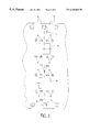
- FIG. 1 shows a conductor track pattern for the connection of the coil
- FIG. 2 shows a conductor track pattern for the contact field
- FIG. 3 shows a pattern of openings in the synthetic foil
- FIG. 4 shows the synthetic foil with glued on conductor tracks.
- FIG. 5 shows a conductor track pattern for the connection of the coil
- FIG. 6 shows a conductor track pattern for the contact field
- FIG. 7 shows a pattern of openings in the synthetic foil
- FIG. 8 shows the synthetic foil with glued on conductor tracks.
- FIG. 1 shows a metal foil 1 with a conductor track pattern for two adjacent integrated circuits. This conductor track pattern is periodically repeated to both sides of the conductor track pattern shown.
- the pattern shown is rotationally symmetrical with respect to the point of intersection of the two axes 9 a and 9 b.
- the metal foil 1 is provided with edge perforations 2 which are made to register with corresponding edge perforations in the synthetic foil during gluing on.
- the openings 3 significantly reduce the cross-section of the metal foil 1 in the direction parallel to the axis 9 b, so that the flexibility in the longitudinal direction of the film strip, i.e. in the direction of the axis 9 a, remains comparatively high after the deposition of the foil 1 on the synthetic foil.
- openings 4 which are bounded by bridges in the metal foil 1 and are slightly larger than the part which, after the deposition of the metal foils on the synthetic foils and the insertion and contacting of integrated circuits, is cut out so as to be inserted into a chip card.
- Projections 5 which form the contact faces for the connection of the two ends of a coil as well as the bonding wires of the integrated circuit after insertion project into the openings 4 . Due to the openings 6 and 7 in the metal foil 1 , the projections 5 are connected to the remainder of the metal foil 1 only via narrow bridges in order to ensure that on the one hand, after cutting out, the connection between the projections 5 and other parts of the metal foil 1 is reliably interrupted and that on the other hand the flexibility in the longitudinal direction, parallel to the axis 9 a, is also improved.
- the distance between the openings 4 is defined by the spacing of the edge perforations in the synthetic foil and the dimensions of the contact field which is shown in detail in FIG. 2 .
- an opening 8 In order to reduce the cross-section of the metal foil 1 at least at short intervals between the openings 4 which succeed one another in the longitudinal direction there is provided an opening 8 whereby the flexibility in the longitudinal direction, parallel to the axis 9 a, is further improved.
- FIG. 2 shows the conductor track pattern for the side of the contact field.
- This conductor track pattern is formed by a metal foil 20 cut out accordingly.
- the pattern shown is again periodically repeated to both sides of the pattern shown, i.e. in the direction of the axis 29 a.
- This conductor track pattern again includes edge perforations 22 to both sides, which perforations are adjoined by larger openings 23 to both sides in the longitudinal direction in order to improve the flexibility.
- the edge perforations 22 and the openings 23 correspond to those in the conductor track pattern shown in FIG. 1 .
- This conductor track pattern comprises essentially contact faces 31 , 32 and 33 which are separated from one another by narrow interruptions 35 . They are connected to one another via narrow bridges only at the area of the edges and at the area of the central axis 29 a. These bridges are interrupted during the afore-mentioned cutting out after the deposition of the integrated circuits.
- the individual contact faces 31 , 32 and 33 have a predetermined shape.
- openings 24 and 25 which reduce the cross-section in the direction parallel to the axis 29 b.
- FIG. 3 shows a section of a synthetic foil 40 onto which the metal foils shown in the FIGS. 1 and 2 are glued.
- the synthetic foil 40 is shaped as a film strip and is provided with edge perforations 42 which are regularly repeated at a distance which is smaller than the period of the conductor track patterns. Between the edges there are shown two openings 43 which, after the metal foil 20 has been glued on, are covered by the conductor track face 33 and in which the integrated circuit is provided on this conductor track face.
- holes 44 which are covered by the conductor track faces 31 , 32 , 33 after the metal foil 20 has been glued on and whereby, after the insertion of the integrated circuit, the contacts thereof are connected to these conductor track segments via bonding wires. Also provided are holes 45 which are covered by the appropriate parts of the projections 5 of the metal foil 1 .
- FIG. 4 shows a part of a film strip where the metal foils shown in the FIGS. 1 and 2, provided with the corresponding conductor track patterns, have been glued onto the synthetic foil shown in FIG. 3 .
- FIG. 4 is a plan view of the conductor track pattern of the metal foil 1 .
- two neighboring conductor track patterns are shown for two integrated circuits each.
- the openings 3 , 23 in the metal foils 1 and 20 respectively, extend across two edge perforations in the synthetic foil 40 of FIG. 3 .
- the position of the openings 43 in FIG. 3 over the conductor face 33 in FIG. 2 and the position of the holes 44 in FIG. 3 over the corresponding conductor faces 31 , 32 and 33 in FIG. 2, denoted by dashed lines in FIG. 4, can be recognized.
- the thin line outside the conductor track faces denoted by dashed lines, represents the cutting line.
- the second embodiment which is shown in the FIGS. 5 to 8 is distinct from the described embodiment shown in the FIGS. 1 to 4 only in respect of a few structural characteristics which will be described in detail hereinafter. The other characteristics of the two embodiments correspond.
- the conductor track pattern of the second embodiment as shown in FIG. 5 deviates first of all in that, instead of the openings 3 , there are now provided openings 10 which extend between each time two successive edge perforations 2 , but do not contact these perforations, so that each of the edge perforations 2 is fully surrounded by metal foil. In the case of optical centering, therefore, all edge perforations 2 have a corresponding structure. In comparison with the first embodiment described, the openings 10 significantly reduce the cross-section of the metal foil in this embodiment in the direction parallel to the axis 9 b.
- a modified contour was also selected for the openings 6 , 7 ; however, in principle this has no effect on the flexibility of the foil according to the invention.
- openings 8 shown in FIG. 1 are absent in the rendition of FIG. 5 . However, such openings may be provided as well for the second embodiment.
- FIG. 6 shows the conductor track pattern for the side of the contact field of the second embodiment.
- no openings are provided between the edge perforations 22 .
- all edge perforations 22 have a uniform border of metal foil.
- the contact faces 31 , 32 , 33 in the second embodiment are formed in conformity with a standard which deviates from that used for the first embodiment and is applied notably in France. Notably the contact faces 31 and 33 are constructed so as to be narrower.
- three openings 27 are provided between the opening 28 and the contact faces 31 and 33 , parallel to the axis 29 b, in addition to the single opening 27 in FIG. 2 at the level of the center of the contact field consisting of the contact faces 31 , 32 , 33 .
- the axis 29 b registers with the axis 9 b in FIG. 5 in the assembled condition of the foil according to the invention.
- the contours of the openings 24 and 25 are also slightly modified. Instead of the openings 25 used thus far in FIG. 2, there are provided two openings 25 , 26 which are symmetrically situated relative to the axis 29 a.
- the synthetic foil 40 of the second embodiment shown in FIG. 7 deviates from the synthetic foil 40 shown in FIG. 3 merely in that the holes 45 are absent. Like the openings 3 and 23 in the first embodiment, the openings 10 which are larger than the edge perforations are not provided in the synthetic foil 40 in the second embodiment.
- FIG. 8 shows a part of a film strip where the metal foils 1 and 20 with the corresponding conductor track patterns, shown in the FIGS. 5 and 6, are glued onto the synthetic foil 40 shown in FIG. 7 .
- FIG. 8 shows the plan view of the conductor track pattern of the metal foil 20 ; for the sake of clarity, again two neighboring conductor track patterns are shown for each time every two integrated circuits.
- the conductor track patterns of the metal foil 1 and the contours of the synthetic foil 40 are denoted by dashed lines at the areas where they are covered by the foils provided thereon, notably the metal foil 20 .
Abstract
Description
Claims (4)
Applications Claiming Priority (3)
| Application Number | Priority Date | Filing Date | Title |
|---|---|---|---|
| DE19816066 | 1998-04-09 | ||
| DE19816066A DE19816066A1 (en) | 1998-04-09 | 1998-04-09 | Foil as a carrier for integrated circuits |
| PCT/IB1999/000591 WO1999053545A1 (en) | 1998-04-09 | 1999-04-07 | Film used as a substrate for integrated circuits |
Publications (1)
| Publication Number | Publication Date |
|---|---|
| US6420660B1 true US6420660B1 (en) | 2002-07-16 |
Family
ID=7864210
Family Applications (1)
| Application Number | Title | Priority Date | Filing Date |
|---|---|---|---|
| US09/445,235 Expired - Lifetime US6420660B1 (en) | 1998-04-09 | 1999-04-07 | Film used as a substrate for integrated circuits |
Country Status (6)
| Country | Link |
|---|---|
| US (1) | US6420660B1 (en) |
| EP (1) | EP0992065B1 (en) |
| JP (1) | JP2002511196A (en) |
| AT (1) | ATE346381T1 (en) |
| DE (2) | DE19816066A1 (en) |
| WO (1) | WO1999053545A1 (en) |
Cited By (2)
| Publication number | Priority date | Publication date | Assignee | Title |
|---|---|---|---|---|
| CN109315064A (en) * | 2016-05-11 | 2019-02-05 | 立联信控股有限公司 | Conductor path structure, in particular for application of IC cards lead frame conductor path structure, at least two stacked conductor path layers |
| US10763203B1 (en) | 2019-02-08 | 2020-09-01 | Nxp B.V. | Conductive trace design for smart card |
Families Citing this family (3)
| Publication number | Priority date | Publication date | Assignee | Title |
|---|---|---|---|---|
| DE10202257B4 (en) | 2002-01-21 | 2005-12-01 | W.C. Heraeus Gmbh | Method for fixing chip carriers |
| WO2004036648A2 (en) * | 2002-10-15 | 2004-04-29 | Axalto Sa | Method of manufacturing a data carrier |
| DE10318688A1 (en) * | 2003-04-24 | 2004-11-25 | W. C. Heraeus Gmbh & Co. Kg | Method for separating the electrical connection nodes in IC frames and method for producing an electronic component and frames therefor |
Citations (12)
| Publication number | Priority date | Publication date | Assignee | Title |
|---|---|---|---|---|
| US3547724A (en) * | 1967-02-07 | 1970-12-15 | Rogers Corp | Method of and apparatus for producing printed circuits |
| US4313152A (en) * | 1979-01-12 | 1982-01-26 | U.S. Philips Corporation | Flat electric coil |
| US4356627A (en) * | 1980-02-04 | 1982-11-02 | Amp Incorporated | Method of making circuit path conductors in plural planes |
| US4555291A (en) * | 1981-04-23 | 1985-11-26 | Minnesota Mining And Manufacturing Company | Method of constructing an LC network |
| JPS6344732A (en) * | 1986-08-11 | 1988-02-25 | Seiko Epson Corp | Manufacture of tape carrier |
| US5023751A (en) * | 1987-06-22 | 1991-06-11 | Eta Sa Fabriques D'ebauches | Method of producing a tape for providing electronic modules, and tape obtained by this method |
| US5119070A (en) * | 1989-01-25 | 1992-06-02 | Tokai Metals Co., Ltd. | Resonant tag |
| US5545922A (en) * | 1994-06-28 | 1996-08-13 | Intel Corporation | Dual sided integrated circuit chip package with offset wire bonds and support block cavities |
| US5550402A (en) * | 1992-11-27 | 1996-08-27 | Esec Sempac S.A. | Electronic module of extra-thin construction |
| US5745988A (en) * | 1994-06-21 | 1998-05-05 | Giesecke & Devrient Gmbh | Method for producing data carriers |
| US6025283A (en) * | 1995-05-12 | 2000-02-15 | The Real Gold Card Company Limited | Charge card |
| US6066231A (en) * | 1995-04-25 | 2000-05-23 | Pem S.A. Protection Electrolytique Des Metaux | Laminating device for joining a metal strip and an insulating material strip |
Family Cites Families (1)
| Publication number | Priority date | Publication date | Assignee | Title |
|---|---|---|---|---|
| FR2579799B1 (en) * | 1985-03-28 | 1990-06-22 | Flonic Sa | METHOD FOR MANUFACTURING ELECTRONIC MEMORY CARDS AND CARDS OBTAINED ACCORDING TO SAID METHOD |
-
1998
- 1998-04-09 DE DE19816066A patent/DE19816066A1/en not_active Withdrawn
-
1999
- 1999-04-07 WO PCT/IB1999/000591 patent/WO1999053545A1/en active IP Right Grant
- 1999-04-07 JP JP55140799A patent/JP2002511196A/en not_active Ceased
- 1999-04-07 US US09/445,235 patent/US6420660B1/en not_active Expired - Lifetime
- 1999-04-07 AT AT99910583T patent/ATE346381T1/en not_active IP Right Cessation
- 1999-04-07 DE DE59913999T patent/DE59913999D1/en not_active Expired - Lifetime
- 1999-04-07 EP EP99910583A patent/EP0992065B1/en not_active Expired - Lifetime
Patent Citations (12)
| Publication number | Priority date | Publication date | Assignee | Title |
|---|---|---|---|---|
| US3547724A (en) * | 1967-02-07 | 1970-12-15 | Rogers Corp | Method of and apparatus for producing printed circuits |
| US4313152A (en) * | 1979-01-12 | 1982-01-26 | U.S. Philips Corporation | Flat electric coil |
| US4356627A (en) * | 1980-02-04 | 1982-11-02 | Amp Incorporated | Method of making circuit path conductors in plural planes |
| US4555291A (en) * | 1981-04-23 | 1985-11-26 | Minnesota Mining And Manufacturing Company | Method of constructing an LC network |
| JPS6344732A (en) * | 1986-08-11 | 1988-02-25 | Seiko Epson Corp | Manufacture of tape carrier |
| US5023751A (en) * | 1987-06-22 | 1991-06-11 | Eta Sa Fabriques D'ebauches | Method of producing a tape for providing electronic modules, and tape obtained by this method |
| US5119070A (en) * | 1989-01-25 | 1992-06-02 | Tokai Metals Co., Ltd. | Resonant tag |
| US5550402A (en) * | 1992-11-27 | 1996-08-27 | Esec Sempac S.A. | Electronic module of extra-thin construction |
| US5745988A (en) * | 1994-06-21 | 1998-05-05 | Giesecke & Devrient Gmbh | Method for producing data carriers |
| US5545922A (en) * | 1994-06-28 | 1996-08-13 | Intel Corporation | Dual sided integrated circuit chip package with offset wire bonds and support block cavities |
| US6066231A (en) * | 1995-04-25 | 2000-05-23 | Pem S.A. Protection Electrolytique Des Metaux | Laminating device for joining a metal strip and an insulating material strip |
| US6025283A (en) * | 1995-05-12 | 2000-02-15 | The Real Gold Card Company Limited | Charge card |
Cited By (3)
| Publication number | Priority date | Publication date | Assignee | Title |
|---|---|---|---|---|
| CN109315064A (en) * | 2016-05-11 | 2019-02-05 | 立联信控股有限公司 | Conductor path structure, in particular for application of IC cards lead frame conductor path structure, at least two stacked conductor path layers |
| CN109315064B (en) * | 2016-05-11 | 2021-10-19 | 立联信控股有限公司 | Conductor path structure with at least two superposed conductor path layers |
| US10763203B1 (en) | 2019-02-08 | 2020-09-01 | Nxp B.V. | Conductive trace design for smart card |
Also Published As
| Publication number | Publication date |
|---|---|
| EP0992065B1 (en) | 2006-11-22 |
| DE59913999D1 (en) | 2007-01-04 |
| ATE346381T1 (en) | 2006-12-15 |
| DE19816066A1 (en) | 1999-10-14 |
| JP2002511196A (en) | 2002-04-09 |
| WO1999053545A1 (en) | 1999-10-21 |
| EP0992065A1 (en) | 2000-04-12 |
Similar Documents
| Publication | Publication Date | Title |
|---|---|---|
| RU2193231C2 (en) | Integrated-circuit module to be implanted in card body with built-in microprocessor (alternatives) | |
| US7285734B2 (en) | Circuit board and method for manufacturing the same and semiconductor device and method for manufacturing the same | |
| US6886247B2 (en) | Circuit board singulation methods | |
| EP0534566B1 (en) | Terminal structure of flexible printed circuit board | |
| US6013945A (en) | Electronic module for data cards | |
| EP1413178B1 (en) | Card manufacturing technique and resulting card | |
| KR100272737B1 (en) | reel printed circuit board and chip on board packages using the reel printed circuit board | |
| KR100487175B1 (en) | Data carrier having a module including an electronic component and having a coil, and method of manufacturing such a data carrier | |
| US6420660B1 (en) | Film used as a substrate for integrated circuits | |
| EP0339154A2 (en) | Memory card | |
| JP3560599B2 (en) | Electronic circuit device | |
| AU2002334330B2 (en) | Electronic circuit comprising conductive bridges and method for making such bridges | |
| US7154048B2 (en) | Common electrode wire for plating | |
| US6081025A (en) | Data carrier with a component-containing module and with a coil, method of producing such a data carrier and module therefor | |
| JPS63318141A (en) | Semiconductor device | |
| US20050245000A1 (en) | PC adapter cards and method of manufacturing the same | |
| US6323526B1 (en) | Semiconductor integrated circuit | |
| US7837120B1 (en) | Modular memory card and method of making same | |
| JP2001202489A (en) | Ic card and its manufacturing method | |
| KR102167855B1 (en) | Method for manufacturing card including coil pattern circuit | |
| KR0145848B1 (en) | Printed circuit board arranged in series | |
| JPH11317428A (en) | Tape carrier and semiconductor device and manufacture of then | |
| JP2632020B2 (en) | Multiple printed wiring board | |
| JPS63160897A (en) | Integrated circuit device | |
| JPS63158764A (en) | Memory cartridge |
Legal Events
| Date | Code | Title | Description |
|---|---|---|---|
| AS | Assignment |
Owner name: U.S. PHILIPS CORPORATION, NEW YORK Free format text: ASSIGNMENT OF ASSIGNORS INTEREST;ASSIGNORS:SAUER, VERONIKA;SLAGER, BEN;LACH, FRIEDRICH;AND OTHERS;REEL/FRAME:010529/0476 Effective date: 19991203 |
|
| STCF | Information on status: patent grant |
Free format text: PATENTED CASE |
|
| FPAY | Fee payment |
Year of fee payment: 4 |
|
| AS | Assignment |
Owner name: NXP B.V., NETHERLANDS Free format text: ASSIGNMENT OF ASSIGNORS INTEREST;ASSIGNOR:U.S. PHILIPS CORPORATION;REEL/FRAME:022973/0397 Effective date: 20090715 |
|
| FPAY | Fee payment |
Year of fee payment: 8 |
|
| AS | Assignment |
Owner name: U.S. PHILIPS CORPORATION, NEW YORK Free format text: CORRECTIVE ASSIGNMENT TO CORRECT THE ASSIGNMENT COVER SHEET OF THE NAME AND ADDRESS OF RECEIVING PARTIES. CO-ASSIGNEES HAD BEEN ERRONEOUSLY OMITTED, PREVIOUSLY RECORDED ON REEL 010529 FRAME 0476. ASSIGNOR(S) HEREBY CONFIRMS THE RECEIVING PARTIES ARE: U.S. PHILIPS CORPORATION, W.C. HERAEUS GMBH & CO KG, AND NEDCARD B.V.;ASSIGNORS:SAUER, VERONIKA;SLAGER, BEN;LACH, FRIEDRICH;AND OTHERS;REEL/FRAME:027697/0331 Effective date: 19991203 Owner name: W.C. HERAEUS & CO KG., GERMANY Free format text: CORRECTIVE ASSIGNMENT TO CORRECT THE ASSIGNMENT COVER SHEET OF THE NAME AND ADDRESS OF RECEIVING PARTIES. CO-ASSIGNEES HAD BEEN ERRONEOUSLY OMITTED, PREVIOUSLY RECORDED ON REEL 010529 FRAME 0476. ASSIGNOR(S) HEREBY CONFIRMS THE RECEIVING PARTIES ARE: U.S. PHILIPS CORPORATION, W.C. HERAEUS GMBH & CO KG, AND NEDCARD B.V.;ASSIGNORS:SAUER, VERONIKA;SLAGER, BEN;LACH, FRIEDRICH;AND OTHERS;REEL/FRAME:027697/0331 Effective date: 19991203 Owner name: NEDCARD B.V., NETHERLANDS Free format text: CORRECTIVE ASSIGNMENT TO CORRECT THE ASSIGNMENT COVER SHEET OF THE NAME AND ADDRESS OF RECEIVING PARTIES. CO-ASSIGNEES HAD BEEN ERRONEOUSLY OMITTED, PREVIOUSLY RECORDED ON REEL 010529 FRAME 0476. ASSIGNOR(S) HEREBY CONFIRMS THE RECEIVING PARTIES ARE: U.S. PHILIPS CORPORATION, W.C. HERAEUS GMBH & CO KG, AND NEDCARD B.V.;ASSIGNORS:SAUER, VERONIKA;SLAGER, BEN;LACH, FRIEDRICH;AND OTHERS;REEL/FRAME:027697/0331 Effective date: 19991203 |
|
| AS | Assignment |
Owner name: W.C. HERAEUS GMBH, GERMANY Free format text: CHANGE OF NAME;ASSIGNOR:W.C. HERAEUS GMBH & CO. KG;REEL/FRAME:027841/0183 Effective date: 20040826 |
|
| AS | Assignment |
Owner name: HERAEUS MATERIALS TECHNOLOGY GMBH & CO. KG., GERMA Free format text: CHANGE OF NAME;ASSIGNOR:W.C. HERAEUS GMBH;REEL/FRAME:027850/0054 Effective date: 20110718 |
|
| FPAY | Fee payment |
Year of fee payment: 12 |
|
| AS | Assignment |
Owner name: HERAEUS DEUTSCHLAND GMBH & CO. KG, GERMANY Free format text: CHANGE OF NAME;ASSIGNOR:HERAEUS MATERIALS TECHNOLOGY GMBH & CO. KG;REEL/FRAME:035744/0381 Effective date: 20141229 |
|
| AS | Assignment |
Owner name: PHILIPS SEMICONDUCTORS INTERNATIONAL B.V., NETHERL Free format text: ASSIGNMENT OF ASSIGNORS INTEREST;ASSIGNOR:KONINKLIJKE PHILIPS ELECTRONICS N.V.;REEL/FRAME:043951/0127 Effective date: 20060928 Owner name: NXP B.V., NETHERLANDS Free format text: CHANGE OF NAME;ASSIGNOR:PHILIPS SEMICONDUCTORS INTERNATIONAL B.V.;REEL/FRAME:043951/0611 Effective date: 20060929 |