US6421131B1 - Birefringent interferometer - Google Patents
Birefringent interferometer Download PDFInfo
- Publication number
- US6421131B1 US6421131B1 US09/607,836 US60783600A US6421131B1 US 6421131 B1 US6421131 B1 US 6421131B1 US 60783600 A US60783600 A US 60783600A US 6421131 B1 US6421131 B1 US 6421131B1
- Authority
- US
- United States
- Prior art keywords
- polarization
- interferometer
- retardance
- variable retarder
- birefringent
- Prior art date
- Legal status (The legal status is an assumption and is not a legal conclusion. Google has not performed a legal analysis and makes no representation as to the accuracy of the status listed.)
- Expired - Fee Related
Links
- 230000010287 polarization Effects 0.000 claims abstract description 64
- 230000003287 optical effect Effects 0.000 claims abstract description 57
- 210000002858 crystal cell Anatomy 0.000 claims abstract description 34
- 239000004988 Nematic liquid crystal Substances 0.000 claims abstract description 8
- 210000004027 cell Anatomy 0.000 claims description 78
- 239000004973 liquid crystal related substance Substances 0.000 claims description 70
- 230000003595 spectral effect Effects 0.000 claims description 34
- 238000000034 method Methods 0.000 claims description 29
- 238000004458 analytical method Methods 0.000 claims description 9
- 238000005259 measurement Methods 0.000 claims description 7
- 230000000295 complement effect Effects 0.000 claims description 5
- 238000009615 fourier-transform spectroscopy Methods 0.000 claims description 3
- CDFSOKHNACTNPU-GHUQRRHWSA-N 3-[(1r,3s,5s,8r,9s,10s,11r,13r,17r)-1,5,11,14-tetrahydroxy-10,13-dimethyl-3-[(2r,3r,4r,5s,6s)-3,4,5-trihydroxy-6-methyloxan-2-yl]oxy-2,3,4,6,7,8,9,11,12,15,16,17-dodecahydro-1h-cyclopenta[a]phenanthren-17-yl]-2h-furan-5-one Chemical compound O[C@@H]1[C@H](O)[C@H](O)[C@H](C)O[C@H]1O[C@@H]1C[C@@]2(O)CC[C@H]3C4(O)CC[C@H](C=5COC(=O)C=5)[C@@]4(C)C[C@@H](O)[C@@H]3[C@@]2(C)[C@H](O)C1 CDFSOKHNACTNPU-GHUQRRHWSA-N 0.000 claims 2
- 238000001228 spectrum Methods 0.000 abstract description 20
- 239000000463 material Substances 0.000 description 22
- 238000003384 imaging method Methods 0.000 description 19
- 230000005540 biological transmission Effects 0.000 description 12
- 230000000694 effects Effects 0.000 description 12
- 239000006185 dispersion Substances 0.000 description 11
- 239000010453 quartz Substances 0.000 description 11
- VYPSYNLAJGMNEJ-UHFFFAOYSA-N silicon dioxide Inorganic materials O=[Si]=O VYPSYNLAJGMNEJ-UHFFFAOYSA-N 0.000 description 11
- 238000010276 construction Methods 0.000 description 10
- 238000013461 design Methods 0.000 description 9
- 230000004044 response Effects 0.000 description 9
- 230000006870 function Effects 0.000 description 8
- 239000000654 additive Substances 0.000 description 7
- 230000000996 additive effect Effects 0.000 description 7
- 238000012544 monitoring process Methods 0.000 description 7
- 230000009466 transformation Effects 0.000 description 7
- 238000013459 approach Methods 0.000 description 6
- 230000008901 benefit Effects 0.000 description 6
- 238000000701 chemical imaging Methods 0.000 description 6
- 239000011521 glass Substances 0.000 description 6
- 230000009471 action Effects 0.000 description 5
- 230000008859 change Effects 0.000 description 5
- 239000000523 sample Substances 0.000 description 5
- 230000001427 coherent effect Effects 0.000 description 4
- 230000005284 excitation Effects 0.000 description 4
- 239000000758 substrate Substances 0.000 description 4
- 239000013078 crystal Substances 0.000 description 3
- 238000011065 in-situ storage Methods 0.000 description 3
- 238000004519 manufacturing process Methods 0.000 description 3
- 238000010183 spectrum analysis Methods 0.000 description 3
- 239000013598 vector Substances 0.000 description 3
- 229910021532 Calcite Inorganic materials 0.000 description 2
- 230000009286 beneficial effect Effects 0.000 description 2
- 238000004364 calculation method Methods 0.000 description 2
- 238000007405 data analysis Methods 0.000 description 2
- 230000007812 deficiency Effects 0.000 description 2
- 230000001066 destructive effect Effects 0.000 description 2
- 230000005684 electric field Effects 0.000 description 2
- 238000005516 engineering process Methods 0.000 description 2
- 239000005262 ferroelectric liquid crystals (FLCs) Substances 0.000 description 2
- 239000007789 gas Substances 0.000 description 2
- 230000007246 mechanism Effects 0.000 description 2
- 230000010363 phase shift Effects 0.000 description 2
- 238000012545 processing Methods 0.000 description 2
- 238000004611 spectroscopical analysis Methods 0.000 description 2
- 238000012935 Averaging Methods 0.000 description 1
- 101100191768 Caenorhabditis elegans pbs-4 gene Proteins 0.000 description 1
- 229920000106 Liquid crystal polymer Polymers 0.000 description 1
- 239000004977 Liquid-crystal polymers (LCPs) Substances 0.000 description 1
- 239000004642 Polyimide Substances 0.000 description 1
- XUIMIQQOPSSXEZ-UHFFFAOYSA-N Silicon Chemical compound [Si] XUIMIQQOPSSXEZ-UHFFFAOYSA-N 0.000 description 1
- 235000010724 Wisteria floribunda Nutrition 0.000 description 1
- 230000032683 aging Effects 0.000 description 1
- 230000001668 ameliorated effect Effects 0.000 description 1
- 238000013528 artificial neural network Methods 0.000 description 1
- 238000000339 bright-field microscopy Methods 0.000 description 1
- 238000000576 coating method Methods 0.000 description 1
- 238000004737 colorimetric analysis Methods 0.000 description 1
- 238000012937 correction Methods 0.000 description 1
- 238000000354 decomposition reaction Methods 0.000 description 1
- 230000000593 degrading effect Effects 0.000 description 1
- 230000001627 detrimental effect Effects 0.000 description 1
- 238000011161 development Methods 0.000 description 1
- 230000018109 developmental process Effects 0.000 description 1
- 238000002059 diagnostic imaging Methods 0.000 description 1
- 230000003292 diminished effect Effects 0.000 description 1
- 230000001747 exhibiting effect Effects 0.000 description 1
- 238000002474 experimental method Methods 0.000 description 1
- 239000004744 fabric Substances 0.000 description 1
- 238000007519 figuring Methods 0.000 description 1
- 238000000684 flow cytometry Methods 0.000 description 1
- 238000000799 fluorescence microscopy Methods 0.000 description 1
- 239000007850 fluorescent dye Substances 0.000 description 1
- 238000010191 image analysis Methods 0.000 description 1
- 238000003709 image segmentation Methods 0.000 description 1
- 238000012625 in-situ measurement Methods 0.000 description 1
- 238000010348 incorporation Methods 0.000 description 1
- 230000003993 interaction Effects 0.000 description 1
- 238000005305 interferometry Methods 0.000 description 1
- 239000010445 mica Substances 0.000 description 1
- 229910052618 mica group Inorganic materials 0.000 description 1
- 238000002156 mixing Methods 0.000 description 1
- 239000000203 mixture Substances 0.000 description 1
- 230000000877 morphologic effect Effects 0.000 description 1
- 239000000382 optic material Substances 0.000 description 1
- 230000005693 optoelectronics Effects 0.000 description 1
- 230000010355 oscillation Effects 0.000 description 1
- 239000004033 plastic Substances 0.000 description 1
- 229920006289 polycarbonate film Polymers 0.000 description 1
- 229920001721 polyimide Polymers 0.000 description 1
- 238000012805 post-processing Methods 0.000 description 1
- 238000000513 principal component analysis Methods 0.000 description 1
- 230000008569 process Effects 0.000 description 1
- 230000006798 recombination Effects 0.000 description 1
- 238000005215 recombination Methods 0.000 description 1
- 238000005070 sampling Methods 0.000 description 1
- 230000035945 sensitivity Effects 0.000 description 1
- 229910052710 silicon Inorganic materials 0.000 description 1
- 239000010703 silicon Substances 0.000 description 1
- 125000006850 spacer group Chemical group 0.000 description 1
- 238000004528 spin coating Methods 0.000 description 1
- 238000006467 substitution reaction Methods 0.000 description 1
- 230000001131 transforming effect Effects 0.000 description 1
- 230000004304 visual acuity Effects 0.000 description 1
Images


Classifications
-
- G—PHYSICS
- G01—MEASURING; TESTING
- G01J—MEASUREMENT OF INTENSITY, VELOCITY, SPECTRAL CONTENT, POLARISATION, PHASE OR PULSE CHARACTERISTICS OF INFRARED, VISIBLE OR ULTRAVIOLET LIGHT; COLORIMETRY; RADIATION PYROMETRY
- G01J3/00—Spectrometry; Spectrophotometry; Monochromators; Measuring colours
- G01J3/28—Investigating the spectrum
- G01J3/447—Polarisation spectrometry
-
- G—PHYSICS
- G01—MEASURING; TESTING
- G01J—MEASUREMENT OF INTENSITY, VELOCITY, SPECTRAL CONTENT, POLARISATION, PHASE OR PULSE CHARACTERISTICS OF INFRARED, VISIBLE OR ULTRAVIOLET LIGHT; COLORIMETRY; RADIATION PYROMETRY
- G01J3/00—Spectrometry; Spectrophotometry; Monochromators; Measuring colours
- G01J3/28—Investigating the spectrum
- G01J3/45—Interferometric spectrometry
- G01J3/453—Interferometric spectrometry by correlation of the amplitudes
-
- G—PHYSICS
- G01—MEASURING; TESTING
- G01J—MEASUREMENT OF INTENSITY, VELOCITY, SPECTRAL CONTENT, POLARISATION, PHASE OR PULSE CHARACTERISTICS OF INFRARED, VISIBLE OR ULTRAVIOLET LIGHT; COLORIMETRY; RADIATION PYROMETRY
- G01J9/00—Measuring optical phase difference; Determining degree of coherence; Measuring optical wavelength
- G01J9/02—Measuring optical phase difference; Determining degree of coherence; Measuring optical wavelength by interferometric methods
-
- G—PHYSICS
- G01—MEASURING; TESTING
- G01J—MEASUREMENT OF INTENSITY, VELOCITY, SPECTRAL CONTENT, POLARISATION, PHASE OR PULSE CHARACTERISTICS OF INFRARED, VISIBLE OR ULTRAVIOLET LIGHT; COLORIMETRY; RADIATION PYROMETRY
- G01J3/00—Spectrometry; Spectrophotometry; Monochromators; Measuring colours
- G01J3/28—Investigating the spectrum
- G01J3/2823—Imaging spectrometer
Definitions
- the field of the invention is spectral imaging, specifically spectral measurement which utilizes optical interference to determine spectral content, and which is capable of determining the spectral content at every point in a one- or two-dimensional image or scene.
- Optical interference is widely used in instruments such as the Michelson interferometer, the Mach-Zender interferometer, the Twyman-Greene interferometer, the Sagnac interferometer, and others. These divide incident light into two or more beams traveling along different paths, which are then recombined. An optical path difference is developed between the paths, which results in constructive or destructive interference, depending on the wavelength of light and on the optical path difference (OPD). The intensity pattern resulting from this interference is termed an interferogram. By observing the interferogram while varying the path difference, one can deduce the wavelength of light present in a monochromatic incident beam, or the amount of each wavelength component in a polychromatic beam. This spectrum is obtained by means of a Fourier transform of the intensity signal, for which reason these instruments are often termed Fourier transform spectrometers, or FTS instruments.
- the spectral resolving power of an FTS instrument depends directly on the range of OPD that can be produced.
- the OPD is varied by mechanical means, such as actuators or piezeo-electric crystals. This involves the motion or rotation of one or more optical elements, such as mirrors or windows, which leads to high cost and complexity given the need to control the OPD variation to a small fraction of a wavelength of light.
- Other means are also used for varying path length.
- an electro-optic material is present in one or more of the optical paths, and the OPD is varied electro-optically. However, this normally results in a limited range of adjustment, as the modulation range of most electro-optic modulators is limited to approximately one wavelength of light.
- one path contains a cell or vessel which may be evacuated or pressurized with gases, to produce an OPD change via the change in refractive index.
- a given pixel on the sensor may correspond with a given point in the scene being imaged for all OPD settings, or it may not.
- an instrument is commercially available from Applied Spectral Imaging, in Migdal Haemek, Israel. In this instrument, the relationship between pixel location and scene location varies as the OPD is changed. A careful accounting must be made to determine which pixel corresponds to which image point, for each different OPD, before the spectra can be calculated.
- Another type of interferometer described by Buican in U.S. Pat. No. 4,905,169 avoids many of the problems of classical interferometers. It uses a photo-elastic modulator (PEM) or equivalent device to imprint a time-varying retardance on a beam of polarized incident light, which then passes through a linear polarizer after which its intensity is measured at a photodetector. By Fourier analysis of the intensity signal, the spectral content of the incident light is determined.
- PEM photo-elastic modulator
- This instrument acts as an interferometer, based on polarization.
- the time-varying retardance is equivalent to an OPD between the components polarized along the ordinary and extraordinary axes of the PEM, and the analysis at the polarizer generates the equivalent of an interferogram.
- Buican's instrument offers the benefits of simplicity, absence of moving parts, and ruggedness. Consequently, it can be built more economically than present-day alternatives.
- PEM devices provide an adequate range of OPD only when operated in resonant mode. This means that the glass or crystal element involved is excited with transducers at or near the frequency of mechanical resonance, which is typically in excess of 10 kHz, and more commonly in the range 50-80 kHz. Since the PEM undergoes an OPD excursion of up to 16 wavelengths, one would need to measure the interferogram intensity a minimum of 32 times per OPD sweep to achieve the Nyquist sampling criterion.
- spectral imaging systems have utilized band-sequential approaches, where an imaging detector is coupled with a spectral filter.
- Examples based on acousto-optic tunable filter (AOTF) elements include Lewis et. al., in U.S. Pat. No. 5,377,003, and Chao et. al. in U.S. Pat. No. 5,216,484.
- AOTF acousto-optic tunable filter
- Kaye teaches in U.S. Pat. No. 4,272,195 a wavelength measuring system comprising a single liquid crystal cell which is driven with a varying voltage while the incident light passes through polarizers on either side of the cell, through the cell, and onto a detector. By adjusting the drive voltage, the retardance of the cell is altered, producing a series of maxima and minima at the detector. The maxima and minima are counted to determine the wavelength of quasi-monochromatic incident light. For light with a finite bandwidth, an estimate of the bandwidth is obtained by observing the decrease in contrast at higher retardances relative to low retardance.
- the system is not capable of spectral analysis, nor of identifying plural wavelengths in an optical beam, as the only information available is the number of maxima and minima during an overall retardance excursion; hence only the mean-center wavelength is sensed.
- Kaye teaches in U.S. Pat. No. 4,444,469 a fluorescence imaging system where a liquid crystal variable retarder is used with polarizers to selectively block a given excitation wavelength, while transmitting nearby wavelengths at which there is fluorescence emission.
- the retardance is stepped by integral multiples of the excitation wavelength, so that the excitation band remains blocked in all cases, while the system exhibits a variety of spectral transmission responses in the emission band.
- Mercer teaches in U.S. Pat. No. 5,689,314 a point-diffraction interferometer which uses liquid crystal material to preferentially introduce a phase shift in the region surrounding a glass or plastic sphere embedded in the liquid crystal material.
- the sphere acts as a pinhole in this non-imaging system.
- Polarized light is divided into a reference beam, which passes through the glass sphere, and an object beam which passes through the liquid crystal material and which may be phase shifted by the electro-optic action of that material.
- the polarization axis of the incident light is parallel to the slow axis of the liquid crystal material, so a pure phase shift is produced, rather than a change in polarization state.
- the apparatus further incorporates an achromatic quarter-wave plate to digitally switch the retardation, wavelength-independently, in quarter-wave steps. Yet this does not ameliorate the problems brought on by discrete OPD steps. Further, since it produces a fixed polarization rotation (on the Poincare sphere), this element effects an OPD that is proportional to wavelength. Since it does not provide the same OPD for all wavelengths (even in the absence of dispersion), but rather provides a constant degree of polarization rotation independent of wavelength, it is not clear whether any meaningful spectral information is gained from the use of this element.
- Miller teaches in U.S. Pat. No. 4,848,877 the use of a monochromatic light beam to determine the retardance of a nematic variable retardance liquid crystal cell while it is in use, or at intervals.
- the beam is polarized prior to entering the liquid crystal cell, preferably at or near an axis of 45 degrees with respect to the liquid crystal director axis. It is then analyzed and its intensity is detected, from which the transmission and cell retardance are determined.
- Prior-art liquid crystal interferometers do not provide a useful field-of-view, or are not thermally rugged, or do not provide continuously variable OPD.
- the fluorescence system of Kaye provides only for collection of fluorescence emission in the face of an excitation signal, without any means for determining the spectrum of emission light. None provides a rugged, economical, precise means for spectral imaging.
- the invention consists of an apparatus and method for providing spectral information via one or more liquid crystal variable retarder cells situated between a pair of polarizers, to form a polarization interferometer that is continuously variable over a substantial range of OPD.
- This interferometer is used together with a detector to read overall intensity while the liquid crystal retardance is varied by known amounts. From the pattern of variation with OPD, the spectrum is obtained using Fourier transform methods.
- the assembly forms an imaging spectrometer that is simple, economical, and capable of precise spectroscopic analysis. It provides nearly diffraction-limited image quality, and can be built using two-dimensional pixelated detectors such as CCD and CID sensors. This arrangement yields spectra for every point in a complex scene, using very simple equipment and conventional imaging detectors.
- the invention preferably includes a reference beam, such as from a laser diode, to provide in-situ monitoring of the OPD.
- a given sensor pixel corresponds to a single scene location, regardless of the OPD setting of the liquid crystal elements. As there are no moving parts, nor any electro-optic deflection, there is no shift in the image as the OPD is varied. Image quality is essentially diffraction-limited. Calibration of wavelength scale is straightforward and reproducible, and there is essentially no thermal drift. Similarly, the calibration of intensity (or transmission) values is direct.
- the polarization interferometer can be placed directly adjacent the detector, for analyzing the spectral quality of luminous or fluorescent objects.
- it may be placed adjacent a lamp and used to filter the light which illuminates a scene; the scene may then be viewed with a detector using essentially conventional optics, and spectra determined for each point in the scene.
- Efficiency of the present invention is approximately 80 percent, broadband. This exceeds the theoretical limit of 50% for interferometers such as Michelson or Sagnac types.
- the instant invention although based on polarization interference, can be constructed to utilize both polarization states of light in an incident beam. Thus, it can achieve throughputs of 80% even for unpolarized scenes. It can therefore be used in low-light settings such as fluorescence without a penalty in efficiency. It can also be used in remote sensing, medical imaging, bright-field microscopy, colorimetry, general spectroscopy, and other applications.
- FIG. 1 depicts the invention, comprising a retardance adjustment unit (RAU) between two polarizers, a photodetector, and control circuitry which reads the photodetector signal, controls the RAU, and determines the spectrum.
- RAU retardance adjustment unit
- FIG. 2 depicts one arrangement for constructing the RAU, incorporating one or more variable-retardance liquid crystal cells in optical series.
- FIG. 3 a depicts an arrangement for constructing the RAU, incorporating two cells and a compensation film for improved off-axis performance.
- FIG. 3 b depicts an arrangement for constructing the RAU, incorporating four cells and a compensation film for improved off-axis performance and/or greater OPD.
- FIG. 3 c depicts another arrangement for constructing the RAU, incorporating multiple compensation films in an alternative approach to compensating off-axis performance.
- FIG. 4 depicts a particular arrangement for incorporating fixed retarders in the RAU, using twisted-nematic cells to switch the sense of the retarders between additive and subtractive with the liquid crystal variable-retardance cells.
- FIG. 5 depicts another arrangement for constructing the RAU with variable-retardance liquid crystal cells and fixed retarder elements such as quartz waveplates, using variable-retardance switching means.
- FIG. 6 depicts the RAU of the current invention, incorporating means for in-situ monitoring of the OPD.
- FIG. 7 depicts the RAU, incorporating polarizing beamsplitters and prisms to utilize both polarizations of incident light.
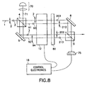
- FIG. 8 depicts the RAU constructed to utilize both polarizations of incident light, along with means for in-situ monitoring of the OPD.
- FIG. 9 a depicts the signal at the detector as the OPD is varied, for several different types of incident light, each monochromatic but having different wavelengths from one another.
- FIG. 9 b depicts the signal at the detector as the OPD is varied, for incident light consisting of several wavelengths at once.
- FIG. 10 depicts the method for calculating the spectrum of incident light using the present invention.
- the invention is an interferometer, consisting of a liquid crystal means for adjusting optical retardance over a range of one wavelength or more, in combination with entrance and analyzer polarizers, a detector, and control electronics. If the incident light is suitably polarized, the entrance polarizer may be omitted.
- the retardance produces an OPD between the optical component which is polarized along the ordinary axis of the liquid crystal material, and the component which is polarized along the extra-ordinary axis.
- These components are made to interfere at the analyzer polarizer, in analogy with a conventional two-beam interferometer such as a Michelson interferometer. It is worth noting, however, that since recombination is achieved without use of beamsplitters, the present invention does not suffer the 50% efficiency loss associated with conventional interferometers.
- the liquid crystal assembly must be constructed to achieve a suitable range of OPD. Also, it must be possible to set the OPD precisely and reproducibly, while varying it over what may be a wide range. Finally, the OPD must be uniform across the aperture and over the field-of-view of the instrument.
- the invention 10 is pictured in FIG. 1, consisting of an input polarizer 11 with transmission axis 14 , a retardance adjustment unit (RAU) 12 with slow axis 15 , an analyzer polarizer 13 with transmission axis 16 , a detector 17 , and control means 18 connected to the detector and the RAU.
- the axes 14 and 16 of the two polarizers are parallel to one another, and oriented at 45 degrees to the slow axis 15 of RAU 12 .
- Incident light 1 is polarized by polarizer 11 so it has an electric field along axis 14 .
- I 0 is the intensity of the beam 1 prior to the polarizer
- k is the transmission efficiency of the polarizer
- R is the retardance of the RAU
- ⁇ is the wavelength of light.
- Equation 3 is the same equation that describes a Michelson interferometer having balanced intensity in the two optical paths.
- This arrangement may be operated as an FTS with an OPD given by the retardance of the RAU element, and it produces identical interferogram data to that of an FTS instrument. It is therefore possible to use all of the prior art developed for imaging and non-imaging FTS instruments in the context of the present invention, including data acquisition, windowing, averaging, and other data analysis methods. These techniques are well-known in the art of spectral instrumentation, and are not recited here. A good introduction is available in Reinhard Beer's Remote Sensing by Fourier Transform Spectroscopy , Wiley-Interscience, New York (1991), but this is not meant as a limitation, since literally all techniques applicable to other FTS instruments may be used in the context of the present invention.
- the present invention may be used with the data analysis techniques of the existing art for transforming interferograms to spectral data. It is similarly appropriate to practice this invention in concert with any other software, analysis, and algorithms that are applicable with other FTS instruments, or which make use of imaging spectral information.
- suitable practices for use with the present invention include any known techniques for spectral analysis, including without limitation principal component analysis, linear decomposition, decorrelated spectral analyis; or image processing, including without limitation image segmentation, object recognition and counting, neural network analysis, development of morphological indices; or combinations of spectral and image analysis as are known to those familiar with the art of remote sensing, biomedical imaging, or machine vision, where these techniques are routinely employed.
- the retardance R arises from the birefringence of liquid crystal material in the RAU, as described below. Accordingly, R (and z) are functions of wavelength due to the inevitable dispersion in birefringence:
- dn( ⁇ ) is the birefringence as a function of wavelength
- n e is the extra-ordinary index of refraction of the liquid crystal material
- n o is the ordinary index of refraction of the liquid crystal material
- OPD ( ⁇ ) OPD ( ⁇ 0 ) [ dn ( ⁇ )/ dn ( ⁇ 0 )] [5]
- ⁇ rescaled ⁇ raw [dn ( ⁇ 0 )/ dn ( ⁇ rescaled )] [6]
- the effect of variations of retardance across the aperture is analogous to variation in OPD produced by wavefront figuring errors in the mirrors of a Michelson interferometer, and may be considered in the same way.
- FIG. 2 A single liquid crystal variable retardance cell 20 is used, which expresses a range of several wavelengths of OPD.
- the cell 20 can be constructed using two substrates 21 and 22 of 0.7 mm thick Corning 7059F glass, the inner surfaces of which have been coated with ITO having a sheet resistivity of 500 ⁇ /square by Donnelly (Holland, Mich.) to form transparent electrodes 23 and 24 .
- the electrodes are then treated to provide a low pretilt alignment using means known in the art, such as spin-coating with polyimide and unidirectional buffing with cloth.
- the substrates are assembled using 13 micron glass spacers from EM Industries (Hawthorne, N.Y.), and filled with liquid crystal material 25 , of type MLC-6080 (EM Industries).
- the resulting cell will display approximately 4 waves of retardance at 633 nm when undriven, dropping continuously for drive voltages above the threshold voltage V th of approximately 2.2 volts, and exhibiting approximately 90 nm retardance when driven with 24 volts. Note that this drawing is not to scale, as the relative thickness of the liquid crystal layer and conductive coatings are greatly expanded relative to the substrates to show detail.
- R is the mean retardance
- X 0 is the mean liquid crystal thickness
- dX is the magnitude of thickness variations across the aperture
- dR is the variation in retardance (OPD) across the aperture.
- the variation across the aperture is proportional to mean retardance, independent of drive level, so a greater absolute error is seen when the cell is driven with a small voltage and expresses a greater total OPD. Conversely, the absolute error is reduced when the cell is driven with a large voltage and expresses a small OPD.
- a pair of pi cells may be placed on either side of a half-wave plate, with the slow axes of the cells at +45° and ⁇ 45° relative to the polarizer transmission axis, and the slow axis of the half-wave plate oriented at 0° or 90°. This is pictured in FIG.
- the RAU incorporates a first cell 30 with its slow axis 33 oriented at 45° relative to the polarization of incident light; a half-wave plate 31 in optical series with its slow axis 34 oriented perpendicular to the polarization axis of incident light; and a second cell 32 in optical series with its slow axis 35 oriented orthogonally to the axis 33 of the first cell 30 .
- the half-wave plate should normally be achromatic over the wavelength range of interest. Methods and materials for the construction of this component are well-known in the art.
- the overall arrangement of cells and half-wave plate is analogous to the wide-field retarder elements used in Lyot filters, and described in The Birefringent Filter, J. Evans J. Opt. Soc. Am., pp. 229-42 (1949).
- the retardance of the cells sums, despite their axes being crossed, because of the action of the half-wave plate between them.
- Half-wave plate 31 has its slow axis 34 oriented at substantially 0° or 90° to the polarization axis 2 .
- cells 32 and 37 have coplanar slow axes 35 and 39 that are oriented orthogonal to axes 33 and 38 of first cells 30 and 36 .
- the effect of z-aligned liquid crystal material can be compensated using other techniques developed in the display industry.
- FIG. 4 Another approach to constructing an RAU is shown in FIG. 4, which permits operation at high OPD without correspondingly tight tolerances on the liquid crystal cells. It includes quartz retarder elements 50 and 51 having slow axes 56 and 57 . Retarder 50 has a retardance of R and retarder 51 has a retardance of 2R. Following these in optical series is a variable-retardance liquid crystal cell or cells 52 having an effective slow axis 58 and a retardance range [0, R]. The slow axes of all these elements are oriented at substantially 45° to the transmission axis 2 of incident light 1 . Liquid crystal switches 53 and 54 are placed between quartz retarders 50 and 51 , and between quartz retarder 51 and liquid crystal retarder 52 , respectively.
- the switches are pictured as twisted-nematic cells with 90° twist, whose director orientations at the entrance faces are given by 59 and 60 , and whose director orientations at the exit faces are given by 62 and 63 . These are parallel and perpendicular, respectively, to the slow axes of the quartz and liquid crystal retarders.
- a final liquid crystal switch 55 has the same arrangement of its entrance and exit face directors 61 and 64 as in cells 53 and 54 .
- This provides means for switching the action of retarders 51 and 52 from being additive with the first quartz retarder 50 , to being subtractive from it.
- the fixed quartz retarders in this type of RAU are chosen to have a binary geometric series of retardances, such as R:2R, etc., and the liquid crystal retarder is adjustable over a range of at least [0, R]. Then, by proper switch settings, one may obtain any value of retardance from 0 to 4R.
- the scheme may be extended with additional fixed retarders to achieve an overall retardance of 2 N+1 R, where N is the number of fixed retarders. In this way, high OPD and high spectral resolution are realized.
- Other retarder value choices may be employed as well, provided that they enable spanning the desired range of overall retardance, or OPD.
- ⁇ n is the birefringence of the liquid crystal mixture
- D is the cell spacing
- ⁇ is the wavelength of light.
- Effectively R switch is the retardance between the two eigenmodes of the twisted nematic cell.
- the cell has no optical action.
- the cell's operation is more complex than this, and it may be modeled using the known art methods, such as to consider the cell as a series of birefringent slabs having different axis orientations from one slab to the next.
- the switches are optically inactive and may be ignored.
- the slow axes 56 and 57 of the fixed retarders 50 and 51 are effectively parallel with the slow axis 58 of variable retarder cell 52 , and all their retardances add. In this way, one may generate OPD values ranging from 3R to 4R, with continuous adjustment possible by variation of the voltage applied to cell 52 .
- the retardation R switch of switch 55 equals that of switch 54 , but its retardance is subtractive, not additive, because it is situated after the 90° coordinate transformation. So, those components which passed through the slow axis of switch 54 will pass through the fast axis of switch 55 and vice versa, and the retardances R switch of switches 54 and 55 cancel.
- Switch 55 introduces its own coordinate transformation of 90° rotation, which makes for a total transformation of 180°, which is indistinguishable from the untransformed state. So, undriven switch 55 corrects for both the coordinate transformation and the retardance introduced by undriven switch 54 .
- the overall result of switches 54 and 55 being undriven is to switch variable retarder 52 from an additive to a subtractive sense. As OPD of variable retarder 52 is varied from 0 to R, the overall OPD varies from 3R to 2R.
- R i is the retardance of the i-th retarder in the assembly.
- the RAU of FIG. 4 may be operated as follows:
- This scheme is quite general, and can be practiced with any desired number of retarders. It is not necessary that the slow axes of the retarders be parallel with one another. If one or more retarders has its fast and slow axes interchanged relative to the above example, it merely changes the sense of that retarder from additive to subtractive, and one must adjust the switch settings accordingly as will be obvious to one skilled in the art of polarized light optics.
- Other materials than quartz may be employed as desired, such as polycarbonate films, mica, calcite, liquid crystal polymer films, and the like.
- switches may be used instead of twisted-nematic type.
- half-wave plates may be used as a suitable switch. These could be used in several ways, such as having a fixed retardance of ⁇ /2 and a slow axis orientation that is selectable between 0° or ⁇ 45°, or 90° and ⁇ / ⁇ 45°; or having a fixed slow axis orientation of 0° or 90° and a variable effective retardance that is selectable between 0 and ⁇ /2. In some arrangements (such as a ⁇ /2 plate having a switchable slow axis between 0° and 45°), the switch introduces a retardance which must be accounted for in calculating the OPD. Use of achromatic half-wave plate designs is favored, as in the prior art apparatus of Sharp et. al. These operate by a different switch mechanism, but produce the same overall effect of switching the various retarders' interaction from being additive in retardance to being subtractive.
- any switch which performs this function may be employed to form an RAU.
- a mechanical switch could be used to engage and disengage the fixed retarder elements, or to rotate their axes to an optically-inactive position.
- Nematic liquid crystal cells, ferroelectric liquid crystal cells, or other electro-optic switch materials may be employed, according to the switching speed requirement, wavelength range, and other factors. All that matters is that the elements' retardance be switched into or out of the beam.
- the RAU of FIG. 5 uses fixed retarders 50 and 51 , and liquid crystal variable retarder 52 as in the previous figure, but with different switching means.
- Switchable half-wave plates 160 , 161 , and 162 having slow axes 163 , 164 , and 165 oriented at 22.5° relative to the polarization vector 2 of incident light 1 are located before fixed retarder 50 , between retarders 50 and 51 , and immediately after retarder 51 .
- the switchable half-wave plates have a fixed slow axis, and a retardance which is selectable between approximately 0 and approximately ⁇ /2. If all the switches express 0 retardance, they are optically inactive and the retardances of elements 50 , 51 , and 52 sum algebraically. Now consider when switches 160 and 161 both express ⁇ /2 retardance and switch 162 expresses 0. Incident light polarized at 0° is reflected to an orientation of 45° by switch 160 ; it passes through retarder 50 entirely along its slow axis 56 and no OPD is developed. It then exits retarder 50 with an orientation of 45° and is reflected by switch 61 to an orientation of 0°.
- Retarder 50 is effectively removed from the system by these switches and may be said to be optically absent.
- switches 160 and 162 express ⁇ /2 and switch 161 expresses 0, both retarders 50 and 51 are optically absent; or, when 161 and 162 express ⁇ /2 and 160 expresses 0, retarder 51 is optically absent.
- Variable retarder 52 always exhibits its OPD. In this way, any desired retardance in the range [0-4R] may be developed.
- Switch 161 Switch 162 Overall OPD setting Setting Setting Setting OPD value [0-R] ⁇ /2 0 ⁇ /2 [0-R] [0-R] ⁇ /2 ⁇ /2 0 [R-2R] [0-R] 0 ⁇ /2 ⁇ /2 [2R-3R] [0-R] 0 0 0 [3R-4R]
- This scheme may be similarly generalized to use with various numbers of fixed retarders having various thicknesses, and various means may be employed for switching.
- various means may be employed for switching.
- achromatic half-wave switches and rotators as well as arrangements using plural cells, fixed compensator or waveplate elements, and combinations thereof, which are familiar to those skilled in the arts of polarization switching and of liquid crystal displays.
- These may be used in place of the switches described above, provided that the effect is to switch in or out the OPD of the fixed retarders, and that any side-effects (such as an OPD shift or coordinate transformation introduced by the switches themselves) can be cancelled by other elements, or corrected for in the overall operation of the interferometer.
- any RAU it is of chief concern that the retardance, or OPD, be well-known in order that accurate interferograms be obtained. This can be achieved using dead-reckoning, where the properties of the liquid crystal elements are well-known by prior calibration, or by means of a non-optical in-situ measurement, such as the capacitance monitoring method described in Miller's U.S. Pat. No. 5,247,378.
- a more accurate measure is obtained by direct optical monitoring as shown in FIG. 6 .
- Light from a substantially monochromatic reference source 70 forms a beam 71 that is polarized along an axis 72 and passes through RAU 12 .
- This polarization may be intrinsic to the source, or it may be produced by polarizer element 73 with polarization axis 69 if the source 70 is unpolarized.
- beam 71 After exiting the RAU, beam 71 passes through an analyzer polarizer 74 and lands on a photodetector 75 , where its intensity is read by control means 18 .
- the transmission axis 76 of the analyzer polarizer is either parallel or perpendicular to the polarization axis 72 , and is normally 45° to the slow axis of the RAU.
- Equation 11a is used when the transmission axis 76 of the analyzer is parallel to polarization axis 72
- 11b is used when axis 65 is substantially perpendicular to polarization axis 72 .
- the result of the measurements and analysis of the reference beam 71 is a table of the RAU's electro-optic response for various applied voltages and switch configurations. This is used to determine the required drive conditions in order to produce a desired OPD in subsequent measurements.
- the beam 71 can be introduced through the main aperture, in time-alternation with the sample beam 1 , by mechanically translating it into and out of the beam. Or, a separate but representative region of the RAU may be dedicated to the reference beam 71 . It may be necessary to provide a shutter means to close off the sample beam 1 during the measurement of the RAU characteristics, if beam 1 interferes with measurements of the reference beam. To minimize interference between these beams, it may be beneficial to reverse the direction of beam 71 and relocate elements 74 and 75 accordingly, so that beam 71 passes through the RAU in reverse direction from the main beam 1 .
- detector 17 When detector 17 is distinct from 75 (or they comprise different spatial regions of the same detector), it may be desirable to use a wavelength ⁇ for the reference beam for which the sample detector 17 is not photoresponsive. Also, one may elect to use a spectral filter at detector 75 that preferentially transmits the monitor beam wavelength ⁇ while not having high transmission at other wavelengths. This reduces the sensitivity to ambient light, and to crosstalk from the sample beam.
- Incident beam 1 contains polarization states 2 and 3 , which are separated into the RAU 12 by means of a reflector 5 .
- beam 6 After passing through the RAU, beam 6 reflects off of a reflector 8 and joins beam 7 at a polarizing beamsplitter 9 .
- the result is that the two beams 6 and 7 corresponding to orthogonal polarization states present in the incident beam are processed in adjacent areas of the RAU, and then recombined without loss.
- polarizing beamsplitters 4 and 9 transmit light having a polarization axis that is coplanar with the normal to the hypotenuse plane of the beamsplitter, and reflect the orthogonal polarization state.
- This means that the overall assembly in FIG. 7 acts to rotate the polarization state of incident beam 1 , and the interference at an OPD of R 0 will be destructive, not constructive.
- the interferograms will therefore have complementary intensity to those of a conventional FTS instrument.
- one may insert a half-wave plate immediately after the RAU, as indicated by element 80 . Its slow axis 81 is oriented at ⁇ 45° relative to the polarization axis 2 of beam 6 .
- the two beams exiting the instrument of FIG. 7 will have some inevitable degree of misalignment, arising from the construction tolerances of the PBS elements and the like. At least one of the mirrors may be made adjustable so that the beams can be registered perfectly. Devices constructed along this design have shown registration errors of less than one pixel across an image of 1030 ⁇ 1300 pixels.
- FIG. 8 shows the incorporation of a reference beam 71 for optical monitoring of RAU by means of the PBS elements.
- Reference beam is introduced at the side face of PBS 4 , where it is split into beams 91 and 92 having polarization axes 93 and 94 , respectively.
- Beam 91 passes directly to the RAU 12 while beam 92 reflects off mirror 5 and then passes to the RAU 12 .
- the polarization state of beams 91 and 92 are transformed to the orthogonal state by achromatic half-wave plate 80 , and then pass to PBS 9 (by way of mirror 8 , in the case of beam 91 ).
- Photodetector 75 measures the intensity of the resulting beam and communicates it to control electronics 18 .
- equation 11a is appropriate. If achromatic half-wave plate 80 is omitted, the complementary signal is obtained, and equation 11b is appropriate.
- the intensity incident upon a single pixel of detector 17 is shown as a function of OPD for monochromatic light of various wavelengths and intensities in FIG. 9 a .
- Light of wavelength 600 nm and intensity 0.25 arbitrary units produces a response shown as 101
- light of 580 nm and like intensity produces a response shown as 102
- light of 650 nm and intensity 0.50 arbitrary units produces a response shown as 103 .
- signals 101 and 102 are exactly out-of-phase at an OPD of 8.7 ⁇ . Each signal produces a response in accord with equation [1].
- an interferogram is developed at each pixel which indicates the spectral emission corresponding to a given point in the object being imaged.
- the interferogram readings must be transformed to a spectrum to yield spectral data.
- This process being identical for each pixel, we will discuss it only in the context of a single-pixel system. However, it will be performed for a great number of pixels when an imaging instrument is contructed. This places great value on achieving computational efficiency, in terms of minimizing the memory requirements, instruction cycles, and so forth that are required.
- the massively parallel nature of the calculation enables the use of hardware and software that are optimized for highly parallel operations.
- the fundamental sequence for instrumental operation is outlined in FIG. 10 for a single pixel. Detector readings are taken while the RAU is stepped through a sequence of OPD values. Typically, the OPD step size will first be chosen in step 100 based on some knowledge of the spectral content of the scene, and will be selected to be small enough to avoid aliasing in accordance with the condition:
- ⁇ z is the OPD step
- ⁇ short and ⁇ long are the shortest and longest wavelengths which may be present in the incident beam 1 .
- the readings are taken in step 101 over the range [0, Z max ], where
- ⁇ is the spectral resolution obtained at a wavelength of ⁇ .
- the resulting readings are analyzed in step 152 according to the inverse Fourier transform, to yield a raw spectrum S( ⁇ raw ).
- This in turn is corrected for dispersion in step 153 using the methods described above, or some other method, to yield a spectrum S( ⁇ true ).
- this consists simply of determining the ordinate for the spectra, which is characteristic of the OPD step and excursion, and of the dispersion of the RAU. The same ordinate applies to all spectra obtained under these conditions, such as all pixels within an image or the like.
- the spectral responsivity of the detector and the instrument are then corrected for in step 154 , to yield a spectrum I( ⁇ true ) with readings that are expressed in units of either relative or absolute intensity.
- the spectrum may then be displayed as in step 155 , or saved for later use as in step 156 , or used as an input to other calculations as in step 157 .
Abstract
Description
| TABLE 1 | ||||
| |
|
|
|
Overall |
| OPD setting | Setting | Setting | Setting | OPD value |
| [R-0] | 90° | 0° | 90° | [0-R] |
| [0-R] | 90° | 90° | 0° | [R-2R] |
| [R-0] | 0° | 90° | 90° | [2R-3R] |
| [0-R] | 0° | 0° | 0° | [3R-4R] |
| TABLE 2 | ||||
| |
|
|
|
Overall |
| OPD setting | Setting | Setting | Setting | OPD value |
| [0-R] | λ/2 | 0 | λ/2 | [0-R] |
| [0-R] | λ/2 | λ/2 | 0 | [R-2R] |
| [0-R] | 0 | λ/2 | λ/2 | [2R-3R] |
| [0-R] | 0 | 0 | 0 | [3R-4R] |
Claims (35)
Priority Applications (1)
| Application Number | Priority Date | Filing Date | Title |
|---|---|---|---|
| US09/607,836 US6421131B1 (en) | 1999-07-02 | 2000-06-30 | Birefringent interferometer |
Applications Claiming Priority (2)
| Application Number | Priority Date | Filing Date | Title |
|---|---|---|---|
| US14228299P | 1999-07-02 | 1999-07-02 | |
| US09/607,836 US6421131B1 (en) | 1999-07-02 | 2000-06-30 | Birefringent interferometer |
Publications (1)
| Publication Number | Publication Date |
|---|---|
| US6421131B1 true US6421131B1 (en) | 2002-07-16 |
Family
ID=22499277
Family Applications (1)
| Application Number | Title | Priority Date | Filing Date |
|---|---|---|---|
| US09/607,836 Expired - Fee Related US6421131B1 (en) | 1999-07-02 | 2000-06-30 | Birefringent interferometer |
Country Status (3)
| Country | Link |
|---|---|
| US (1) | US6421131B1 (en) |
| EP (1) | EP1200796A1 (en) |
| WO (1) | WO2001002799A1 (en) |
Cited By (65)
| Publication number | Priority date | Publication date | Assignee | Title |
|---|---|---|---|---|
| US6490043B1 (en) * | 2000-02-14 | 2002-12-03 | Aerodyne Research, Inc. | Polarimetric spectral intensity modulation spectropolarimeter |
| US20030067641A1 (en) * | 2001-08-14 | 2003-04-10 | Terapulse, Inc. | Apparatus and methods for polarization measurements across a spectral range |
| US6552836B2 (en) * | 2000-08-31 | 2003-04-22 | Cambridge Research & Instrumentation, Inc. | High performance polarization controller and polarization sensor |
| US20030095313A1 (en) * | 2001-09-27 | 2003-05-22 | Terapulse, Inc. | Methods and apparatus for higher-order compensation of transmission distortions in optical transmission media |
| US20030219250A1 (en) * | 2002-04-10 | 2003-11-27 | Wein Steven J. | Optical signal-to-noise monitor having increased coherence |
| US20030231390A1 (en) * | 2002-03-15 | 2003-12-18 | Wein Steven J. | Athermal delay line |
| US6784416B2 (en) * | 2001-12-31 | 2004-08-31 | 3M Innovative Properties Company | Polarization transformer and polarization mode dispersion compensator |
| US20040212800A1 (en) * | 2003-04-28 | 2004-10-28 | National Taiwan University Of Science And Technology | Simultaneous optical isolation and channel monitoring system |
| US6856710B2 (en) | 2001-03-19 | 2005-02-15 | Terapulse, Inc. | Polarization mode dispersion compensation in optical transmission media |
| US6867863B1 (en) * | 1999-03-31 | 2005-03-15 | Hinds Instruments | Integrated diagnostic for photoelastic modulator |
| US6947193B1 (en) * | 1999-12-17 | 2005-09-20 | Deutsche Telekom Ag | Optical phase modulator |
| US20060038999A1 (en) * | 2002-10-25 | 2006-02-23 | Christian Hentschel | Polarization conversion unit for reducing polarization dependent measurement errors |
| US20060038929A1 (en) * | 2004-08-18 | 2006-02-23 | Chenhui Wang | Tunable spectral imaging filter configured for UV spectral ranges |
| US7006234B1 (en) * | 2002-01-09 | 2006-02-28 | Interphase Technologies, Inc. | Common-path point-diffraction phase-shifting interferometer incorporating a birefringent polymer membrane |
| US7106456B1 (en) * | 2002-01-09 | 2006-09-12 | Interphase Technologies, Inc. | Common-path point-diffraction phase-shifting interferometer |
| US20060245631A1 (en) * | 2005-01-27 | 2006-11-02 | Richard Levenson | Classifying image features |
| US7132636B1 (en) * | 2001-07-06 | 2006-11-07 | Palantyr Research, Llc | Imaging system and methodology employing reciprocal space optical design |
| US20070016082A1 (en) * | 2003-09-23 | 2007-01-18 | Richard Levenson | Spectral imaging |
| US20070070354A1 (en) * | 2005-09-07 | 2007-03-29 | Tien-Hsin Chao | Electro-Optic Imaging Fourier Transform Spectrometer |
| US20070070260A1 (en) * | 2005-09-27 | 2007-03-29 | Xinghua Wang | Liquid crystal filter with tunable rejection band |
| US20070086017A1 (en) * | 2005-10-07 | 2007-04-19 | Bioptigen, Inc. | Imaging Systems Using Unpolarized Light And Related Methods And Controllers |
| US20070139772A1 (en) * | 2005-12-21 | 2007-06-21 | Xinghua Wang | Optical birefringence filters with interleaved absorptive and zero degree reflective polarizers |
| US20070166045A1 (en) * | 2006-01-09 | 2007-07-19 | Xinghua Wang | Birefringent spectral filter with wide field of view and associated communications method and apparatus |
| US20080007813A1 (en) * | 2005-02-02 | 2008-01-10 | Chemimage Corporation | Multi-conjugate liquid crystal tunable filter |
| US20080074649A1 (en) * | 2006-09-25 | 2008-03-27 | Cambridge Research And Instrumentation, Inc. | Sample imaging and classification |
| US20080144177A1 (en) * | 2006-11-30 | 2008-06-19 | Cambridge Research & Instrumentation, Inc. | Optical filter assembly with selectable bandwidth and rejection |
| US7417796B2 (en) | 2006-09-29 | 2008-08-26 | Chemimage Corporation | Wavelength discrimination filter for infrared wavelengths |
| US20080294032A1 (en) * | 2003-09-23 | 2008-11-27 | Cambridge Research And Instrumentation, Inc. | Spectral Imaging of Biological Samples |
| US20090096914A1 (en) * | 2007-10-16 | 2009-04-16 | Domenicali Peter L | Spectral imaging system with dynamic optical correction |
| US20090257640A1 (en) * | 2008-03-10 | 2009-10-15 | Kirk William Gossage | Classification of samples |
| US20090257028A1 (en) * | 2006-10-16 | 2009-10-15 | Asahi Glass Company, Limited | Projection type display device |
| US20090324051A1 (en) * | 2008-06-17 | 2009-12-31 | Hoyt Clifford C | Image Classifier Training |
| US20100034453A1 (en) * | 2008-08-07 | 2010-02-11 | David Lynch | Detection of rna in tissue samples |
| US20100075373A1 (en) * | 2008-09-22 | 2010-03-25 | Hoyt Clifford C | Multi-Spectral Imaging Including At Least One Common Stain |
| US20110182490A1 (en) * | 2009-08-10 | 2011-07-28 | Hoyt Clifford C | Visualization of stained samples |
| US20110292402A1 (en) * | 2009-02-13 | 2011-12-01 | National University Corporation Kyoto Institute Of Technology | Interference measurement apparatus and method for measuring interference |
| US20110299089A1 (en) * | 2010-06-04 | 2011-12-08 | University Of Washington | Compact liquid crystal based fourier transform spectrometer system |
| US20120087500A1 (en) * | 2010-10-06 | 2012-04-12 | Sony Corporation | Quantum encryption communication apparatus, quantum encryption communication method, and quantum encryption communication system |
| CN102706461A (en) * | 2012-05-28 | 2012-10-03 | 中国电子科技集团公司第四十一研究所 | Novel Mach-Zehnder polarized beam splitting interferometer |
| US8400574B2 (en) | 2010-04-16 | 2013-03-19 | Chemimage Corporation | Short wave infrared multi-conjugate liquid crystal tunable filter |
| US8462981B2 (en) | 2010-04-07 | 2013-06-11 | Cambridge Research & Instrumentation, Inc. | Spectral unmixing for visualization of samples |
| CN103196658A (en) * | 2013-04-19 | 2013-07-10 | 山东大学 | Method and device for measuring phase delay spectral characteristic of wave plate |
| WO2014064701A1 (en) * | 2012-10-26 | 2014-05-01 | Applied Spectral Imaging Ltd. | Method and system for spectral imaging |
| US8736777B2 (en) | 2011-01-19 | 2014-05-27 | Chemimage Technologies Llc | VIS-SNIR multi-conjugate liquid crystal tunable filter |
| US20140247449A1 (en) * | 2013-03-01 | 2014-09-04 | Sandia Corporation | Athermal channeled spectropolarimeter |
| US9256013B2 (en) | 2011-04-14 | 2016-02-09 | Chemimage Technologies Llc | Short-wavelength infrared (SWIR) multi-conjugate liquid crystal tunable filter |
| US20160048040A1 (en) * | 2004-01-28 | 2016-02-18 | Pamela Saha | Deformable photoelastic device |
| US9316539B1 (en) | 2015-03-10 | 2016-04-19 | LightHaus Photonics Pte. Ltd. | Compact spectrometer |
| US9316540B1 (en) | 2015-02-16 | 2016-04-19 | LightHaus Photonics Pte. Ltd. | Compact spectrometer |
| EP3015832A1 (en) * | 2014-10-29 | 2016-05-04 | Palo Alto Research Center, Incorporated | Liquid crystal fourier transform imaging spectrometer |
| US20160124250A1 (en) * | 2013-05-23 | 2016-05-05 | President And Fellows Of Harvard College | Pixelated tunable color filter |
| US20160127661A1 (en) * | 2014-10-29 | 2016-05-05 | Palo Alto Research Center Incorporated | Liquid crystal fourier transform imaging spectrometer |
| US20160127660A1 (en) * | 2014-10-29 | 2016-05-05 | Palo Alto Research Center Incorporated | Liquid crystal fourier transform imaging spectrometer |
| US20160178503A1 (en) * | 2014-12-18 | 2016-06-23 | Palo Alto Research Center Incorporated | Obtaining spectral information from moving objects |
| US9541504B2 (en) | 2010-08-05 | 2017-01-10 | Cambridge Research & Instrumentation, Inc. | Enhancing visual assessment of samples |
| US20180095307A1 (en) * | 2016-10-03 | 2018-04-05 | Xerox Corporation | Hyperspectral imaging system |
| US10175116B1 (en) | 2017-12-29 | 2019-01-08 | Palo Alto Research Center Incorporated | Color filter used with liquid-crystal polarization interferometer |
| US10302494B2 (en) | 2014-12-18 | 2019-05-28 | Palo Alto Research Center Incorporated | Obtaining spectral information from a moving object |
| US20190162999A1 (en) * | 2017-11-30 | 2019-05-30 | Palo Alto Research Center Incorporated | Liquid-crystal variable retarder using liquid crystal cells of differing thicknesses |
| US10663346B2 (en) | 2017-12-29 | 2020-05-26 | Palo Alto Research Center Incorporated | Method and apparatus for transforming uniformly or non-uniformly sampled interferograms to produce spectral data |
| CN111707367A (en) * | 2020-05-08 | 2020-09-25 | 中国科学院西安光学精密机械研究所 | Polarization spectrum imaging device and method based on M-Z interference |
| US10983338B2 (en) | 2017-12-29 | 2021-04-20 | Palo Alto Research Center Incorporated | Exit-pupil expander used distribute light over a liquid-crystal variable retarder |
| US11143556B1 (en) * | 2020-06-07 | 2021-10-12 | Evgueni Vladimirovich Ivanov | Birefringent interferometer and fourier transform spectrometer |
| DE102021207184A1 (en) | 2020-07-17 | 2022-01-20 | Georg Herink | Optical assembly for interferometric measurement |
| WO2022240492A1 (en) * | 2021-05-14 | 2022-11-17 | Becton, Dickinson And Company | Systems for detecting light by birefringent fourier transform interferometry and methods for using same |
Families Citing this family (6)
| Publication number | Priority date | Publication date | Assignee | Title |
|---|---|---|---|---|
| JP2004526331A (en) | 2001-05-15 | 2004-08-26 | カール・ツアイス・エスエムテイ・アーゲー | Objective lens including fluoride crystal lens |
| JP3639807B2 (en) | 2001-06-27 | 2005-04-20 | キヤノン株式会社 | Optical element and manufacturing method |
| EP1278050A1 (en) * | 2001-07-18 | 2003-01-22 | C.S.E.M. Centre Suisse D'electronique Et De Microtechnique Sa | Polarization interferometer with reduced noise |
| EP1278049A1 (en) * | 2001-07-18 | 2003-01-22 | CSEM Centre Suisse d'Electronique et de Microtechnique SA | Illumination module for a reflection spectrometer |
| EP2759812B1 (en) | 2013-01-29 | 2018-01-17 | Rechner Industrie-Elektronik GmbH | Method and apparatus for capacitative fill level measurement of liquids or bulk materials |
| DE102017204888B4 (en) | 2017-03-23 | 2020-11-19 | Robert Bosch Gmbh | Fourier transform spectrometer and method of operating a Fourier transform spectrometer |
Citations (18)
| Publication number | Priority date | Publication date | Assignee | Title |
|---|---|---|---|---|
| US4272195A (en) * | 1979-06-05 | 1981-06-09 | Beckman Instruments, Inc. | Method and apparatus for determining the wavelength of light |
| US4394069A (en) | 1979-06-05 | 1983-07-19 | Beckman Instruments, Inc. | Liquid crystal tuned birefringent filter |
| US4444469A (en) | 1979-06-05 | 1984-04-24 | Beckman Instruments, Inc. | Narrow band rejection filter utilizing a liquid crystal cell |
| US4497542A (en) | 1979-06-05 | 1985-02-05 | Beckman Instruments, Inc. | Apparatus for minimizing beam collimation sensitivity in optical instruments including liquid crystal cells |
| US4848877A (en) | 1987-09-29 | 1989-07-18 | Cambridge Research And Instrumentation, Inc. | Liquid crystal devices and systems using such devices |
| US4905169A (en) | 1988-06-02 | 1990-02-27 | The United States Of America As Represented By The United States Department Of Energy | Method and apparatus for simultaneously measuring a plurality of spectral wavelengths present in electromagnetic radiation |
| US5117466A (en) | 1991-04-30 | 1992-05-26 | The United States Of America As Represented By The United States Department Of Energy | Integrated fluorescence analysis system |
| US5132826A (en) * | 1989-10-30 | 1992-07-21 | The University Of Colorado Foundation, Inc. | Ferroelectric liquid crystal tunable filters and color generation |
| US5216484A (en) | 1991-12-09 | 1993-06-01 | The United States Of America As Represented By The Administrator Of The National Aeronautics And Space Administration | Real-time imaging spectrometer |
| US5247378A (en) * | 1991-06-07 | 1993-09-21 | Peter Miller | Optical retarder having means for determining the retardance of the cell corresponding to the sensed capacitance thereof |
| US5377003A (en) | 1992-03-06 | 1994-12-27 | The United States Of America As Represented By The Department Of Health And Human Services | Spectroscopic imaging device employing imaging quality spectral filters |
| US5539517A (en) | 1993-07-22 | 1996-07-23 | Numetrix Ltd. | Method for simultaneously measuring the spectral intensity as a function of wavelength of all the pixels of a two dimensional scene |
| US5600440A (en) | 1995-07-05 | 1997-02-04 | The United States Of America As Represented By The Secretary Of The Navy | Liquid crystal interferometer |
| US5689314A (en) | 1995-06-14 | 1997-11-18 | The United States Of America As Represented By The Administrator Of The National Aeronautics And Space Administration | Common path point diffraction interferometer using liquid crystal phase shifting |
| US5784162A (en) | 1993-08-18 | 1998-07-21 | Applied Spectral Imaging Ltd. | Spectral bio-imaging methods for biological research, medical diagnostics and therapy |
| US5835214A (en) | 1991-02-22 | 1998-11-10 | Applied Spectral Imaging Ltd. | Method and apparatus for spectral analysis of images |
| US5838441A (en) | 1997-07-23 | 1998-11-17 | The United States Of America As Represented By The National Security Agency | Wide field of view coherent light detector and locator |
| US5841536A (en) * | 1997-08-01 | 1998-11-24 | The United States Of America As Represented By The Director Of The National Security Agency | Polarization interferometer apparatus using the polarization dependent phase lag in a birefringent retarder |
-
2000
- 2000-06-30 WO PCT/US2000/018193 patent/WO2001002799A1/en not_active Application Discontinuation
- 2000-06-30 EP EP00950278A patent/EP1200796A1/en not_active Withdrawn
- 2000-06-30 US US09/607,836 patent/US6421131B1/en not_active Expired - Fee Related
Patent Citations (18)
| Publication number | Priority date | Publication date | Assignee | Title |
|---|---|---|---|---|
| US4394069A (en) | 1979-06-05 | 1983-07-19 | Beckman Instruments, Inc. | Liquid crystal tuned birefringent filter |
| US4444469A (en) | 1979-06-05 | 1984-04-24 | Beckman Instruments, Inc. | Narrow band rejection filter utilizing a liquid crystal cell |
| US4497542A (en) | 1979-06-05 | 1985-02-05 | Beckman Instruments, Inc. | Apparatus for minimizing beam collimation sensitivity in optical instruments including liquid crystal cells |
| US4272195A (en) * | 1979-06-05 | 1981-06-09 | Beckman Instruments, Inc. | Method and apparatus for determining the wavelength of light |
| US4848877A (en) | 1987-09-29 | 1989-07-18 | Cambridge Research And Instrumentation, Inc. | Liquid crystal devices and systems using such devices |
| US4905169A (en) | 1988-06-02 | 1990-02-27 | The United States Of America As Represented By The United States Department Of Energy | Method and apparatus for simultaneously measuring a plurality of spectral wavelengths present in electromagnetic radiation |
| US5132826A (en) * | 1989-10-30 | 1992-07-21 | The University Of Colorado Foundation, Inc. | Ferroelectric liquid crystal tunable filters and color generation |
| US5835214A (en) | 1991-02-22 | 1998-11-10 | Applied Spectral Imaging Ltd. | Method and apparatus for spectral analysis of images |
| US5117466A (en) | 1991-04-30 | 1992-05-26 | The United States Of America As Represented By The United States Department Of Energy | Integrated fluorescence analysis system |
| US5247378A (en) * | 1991-06-07 | 1993-09-21 | Peter Miller | Optical retarder having means for determining the retardance of the cell corresponding to the sensed capacitance thereof |
| US5216484A (en) | 1991-12-09 | 1993-06-01 | The United States Of America As Represented By The Administrator Of The National Aeronautics And Space Administration | Real-time imaging spectrometer |
| US5377003A (en) | 1992-03-06 | 1994-12-27 | The United States Of America As Represented By The Department Of Health And Human Services | Spectroscopic imaging device employing imaging quality spectral filters |
| US5539517A (en) | 1993-07-22 | 1996-07-23 | Numetrix Ltd. | Method for simultaneously measuring the spectral intensity as a function of wavelength of all the pixels of a two dimensional scene |
| US5784162A (en) | 1993-08-18 | 1998-07-21 | Applied Spectral Imaging Ltd. | Spectral bio-imaging methods for biological research, medical diagnostics and therapy |
| US5689314A (en) | 1995-06-14 | 1997-11-18 | The United States Of America As Represented By The Administrator Of The National Aeronautics And Space Administration | Common path point diffraction interferometer using liquid crystal phase shifting |
| US5600440A (en) | 1995-07-05 | 1997-02-04 | The United States Of America As Represented By The Secretary Of The Navy | Liquid crystal interferometer |
| US5838441A (en) | 1997-07-23 | 1998-11-17 | The United States Of America As Represented By The National Security Agency | Wide field of view coherent light detector and locator |
| US5841536A (en) * | 1997-08-01 | 1998-11-24 | The United States Of America As Represented By The Director Of The National Security Agency | Polarization interferometer apparatus using the polarization dependent phase lag in a birefringent retarder |
Non-Patent Citations (1)
| Title |
|---|
| Multispectral imaging with a liquid crystal tunable filter, Miller et al, SPIE vol. 2345, 1995, pp. 354-365. * |
Cited By (125)
| Publication number | Priority date | Publication date | Assignee | Title |
|---|---|---|---|---|
| US6867863B1 (en) * | 1999-03-31 | 2005-03-15 | Hinds Instruments | Integrated diagnostic for photoelastic modulator |
| US6947193B1 (en) * | 1999-12-17 | 2005-09-20 | Deutsche Telekom Ag | Optical phase modulator |
| US6490043B1 (en) * | 2000-02-14 | 2002-12-03 | Aerodyne Research, Inc. | Polarimetric spectral intensity modulation spectropolarimeter |
| US6552836B2 (en) * | 2000-08-31 | 2003-04-22 | Cambridge Research & Instrumentation, Inc. | High performance polarization controller and polarization sensor |
| US6856710B2 (en) | 2001-03-19 | 2005-02-15 | Terapulse, Inc. | Polarization mode dispersion compensation in optical transmission media |
| US7132636B1 (en) * | 2001-07-06 | 2006-11-07 | Palantyr Research, Llc | Imaging system and methodology employing reciprocal space optical design |
| US20030067641A1 (en) * | 2001-08-14 | 2003-04-10 | Terapulse, Inc. | Apparatus and methods for polarization measurements across a spectral range |
| US20030095313A1 (en) * | 2001-09-27 | 2003-05-22 | Terapulse, Inc. | Methods and apparatus for higher-order compensation of transmission distortions in optical transmission media |
| US6784416B2 (en) * | 2001-12-31 | 2004-08-31 | 3M Innovative Properties Company | Polarization transformer and polarization mode dispersion compensator |
| US7006234B1 (en) * | 2002-01-09 | 2006-02-28 | Interphase Technologies, Inc. | Common-path point-diffraction phase-shifting interferometer incorporating a birefringent polymer membrane |
| US7106456B1 (en) * | 2002-01-09 | 2006-09-12 | Interphase Technologies, Inc. | Common-path point-diffraction phase-shifting interferometer |
| US20030231390A1 (en) * | 2002-03-15 | 2003-12-18 | Wein Steven J. | Athermal delay line |
| US7106443B2 (en) | 2002-04-10 | 2006-09-12 | Lighthouse Capital Partners, Inc. | Optical signal-to-noise monitor having increased coherence |
| US20030219250A1 (en) * | 2002-04-10 | 2003-11-27 | Wein Steven J. | Optical signal-to-noise monitor having increased coherence |
| US20060038999A1 (en) * | 2002-10-25 | 2006-02-23 | Christian Hentschel | Polarization conversion unit for reducing polarization dependent measurement errors |
| US20040212800A1 (en) * | 2003-04-28 | 2004-10-28 | National Taiwan University Of Science And Technology | Simultaneous optical isolation and channel monitoring system |
| US6947139B2 (en) | 2003-04-28 | 2005-09-20 | National Taiwan University Of Science And Technology | Simultaneous optical isolation and channel monitoring system |
| US8634607B2 (en) | 2003-09-23 | 2014-01-21 | Cambridge Research & Instrumentation, Inc. | Spectral imaging of biological samples |
| US20080294032A1 (en) * | 2003-09-23 | 2008-11-27 | Cambridge Research And Instrumentation, Inc. | Spectral Imaging of Biological Samples |
| US8385615B2 (en) | 2003-09-23 | 2013-02-26 | Cambridge Research & Instrumentation, Inc. | Spectral imaging of biological samples |
| US8391961B2 (en) | 2003-09-23 | 2013-03-05 | Cambridge Research & Instrumentation, Inc. | Spectral imaging |
| US20070016082A1 (en) * | 2003-09-23 | 2007-01-18 | Richard Levenson | Spectral imaging |
| US8879812B2 (en) | 2003-09-23 | 2014-11-04 | Cambridge Research & Instrumentation, Inc. | Spectral imaging of biological samples |
| US9588099B2 (en) | 2003-09-23 | 2017-03-07 | Cambridge Research & Intrumentation, Inc. | Spectral imaging |
| US20090245605A1 (en) * | 2003-09-23 | 2009-10-01 | Richard Levenson | Spectral imaging of biological samples |
| US20160048040A1 (en) * | 2004-01-28 | 2016-02-18 | Pamela Saha | Deformable photoelastic device |
| US10539813B2 (en) * | 2004-01-28 | 2020-01-21 | Pamela Saha | Deformable photoelastic device |
| WO2006023528A2 (en) * | 2004-08-18 | 2006-03-02 | Chemimage Corp. | Tunable spectral imaging filter configured for uv spectral ranges |
| US20060038929A1 (en) * | 2004-08-18 | 2006-02-23 | Chenhui Wang | Tunable spectral imaging filter configured for UV spectral ranges |
| WO2006023528A3 (en) * | 2004-08-18 | 2006-06-08 | Chemimage Corp | Tunable spectral imaging filter configured for uv spectral ranges |
| US7555155B2 (en) | 2005-01-27 | 2009-06-30 | Cambridge Research & Instrumentation, Inc. | Classifying image features |
| US20090297016A1 (en) * | 2005-01-27 | 2009-12-03 | Richard Levenson | Classifying image features |
| US8280140B2 (en) * | 2005-01-27 | 2012-10-02 | Cambridge Research & Instrumentation, Inc. | Classifying image features |
| US7953264B2 (en) * | 2005-01-27 | 2011-05-31 | Cambridge Research & Instrumentation, Inc. | Classifying image features |
| US20060245631A1 (en) * | 2005-01-27 | 2006-11-02 | Richard Levenson | Classifying image features |
| US8639043B2 (en) | 2005-01-27 | 2014-01-28 | Cambridge Research & Instrumentation, Inc. | Classifying image features |
| US20110255753A1 (en) * | 2005-01-27 | 2011-10-20 | Richard Levenson | Classifying image features |
| US20080007813A1 (en) * | 2005-02-02 | 2008-01-10 | Chemimage Corporation | Multi-conjugate liquid crystal tunable filter |
| US7362489B2 (en) | 2005-02-02 | 2008-04-22 | Chemimage Corporation | Multi-conjugate liquid crystal tunable filter |
| US20070070354A1 (en) * | 2005-09-07 | 2007-03-29 | Tien-Hsin Chao | Electro-Optic Imaging Fourier Transform Spectrometer |
| US7639363B2 (en) * | 2005-09-07 | 2009-12-29 | California Institute Of Technology | Electro-optic imaging Fourier transform spectrometer |
| US7336323B2 (en) | 2005-09-27 | 2008-02-26 | Chemimage Corporation | Liquid crystal filter with tunable rejection band |
| US20070070260A1 (en) * | 2005-09-27 | 2007-03-29 | Xinghua Wang | Liquid crystal filter with tunable rejection band |
| US20080111930A1 (en) * | 2005-09-27 | 2008-05-15 | Chemimage Corporation | Liquid crystal filter with tunable rejection band |
| US7545504B2 (en) | 2005-10-07 | 2009-06-09 | Biotigen, Inc. | Imaging systems using unpolarized light and related methods and controllers |
| US20070086017A1 (en) * | 2005-10-07 | 2007-04-19 | Bioptigen, Inc. | Imaging Systems Using Unpolarized Light And Related Methods And Controllers |
| US20070139772A1 (en) * | 2005-12-21 | 2007-06-21 | Xinghua Wang | Optical birefringence filters with interleaved absorptive and zero degree reflective polarizers |
| US7859753B2 (en) | 2005-12-21 | 2010-12-28 | Chem Image Corporation | Optical birefringence filters with interleaved absorptive and zero degree reflective polarizers |
| WO2007082202A2 (en) * | 2006-01-09 | 2007-07-19 | Chemimage Corporation | Birefringent spectral filter with wide field of view and associated communications method and apparatus |
| WO2007082202A3 (en) * | 2006-01-09 | 2008-07-24 | Chemimage Corp | Birefringent spectral filter with wide field of view and associated communications method and apparatus |
| US7848000B2 (en) | 2006-01-09 | 2010-12-07 | Chemimage Corporation | Birefringent spectral filter with wide field of view and associated communications method and apparatus |
| US20070166045A1 (en) * | 2006-01-09 | 2007-07-19 | Xinghua Wang | Birefringent spectral filter with wide field of view and associated communications method and apparatus |
| US20080074649A1 (en) * | 2006-09-25 | 2008-03-27 | Cambridge Research And Instrumentation, Inc. | Sample imaging and classification |
| US9262697B2 (en) | 2006-09-25 | 2016-02-16 | Cambridge Research & Instrumentation, Inc. | Sample imaging and classification |
| US8126205B2 (en) | 2006-09-25 | 2012-02-28 | Cambridge Research & Instrumentation, Inc. | Sample imaging and classification |
| US20090046363A1 (en) * | 2006-09-29 | 2009-02-19 | Chemimage Corporation | Wavelength discrimination filter for infrared wavelengths |
| US7417796B2 (en) | 2006-09-29 | 2008-08-26 | Chemimage Corporation | Wavelength discrimination filter for infrared wavelengths |
| US8132917B2 (en) * | 2006-10-16 | 2012-03-13 | Asahi Glass Company, Limited | Projection type display device with a phase modulating unit |
| JP5136419B2 (en) * | 2006-10-16 | 2013-02-06 | 旭硝子株式会社 | Projection display |
| US20090257028A1 (en) * | 2006-10-16 | 2009-10-15 | Asahi Glass Company, Limited | Projection type display device |
| US7655898B2 (en) * | 2006-11-30 | 2010-02-02 | Cambridge Research & Instrumentation, Inc. | Optical filter assembly with selectable bandwidth and rejection |
| US20080144177A1 (en) * | 2006-11-30 | 2008-06-19 | Cambridge Research & Instrumentation, Inc. | Optical filter assembly with selectable bandwidth and rejection |
| US20090096914A1 (en) * | 2007-10-16 | 2009-04-16 | Domenicali Peter L | Spectral imaging system with dynamic optical correction |
| US8330087B2 (en) | 2007-10-16 | 2012-12-11 | Cambridge Research & Instrumentation, Inc. | Spectral imaging system with dynamic optical correction |
| US8103081B2 (en) * | 2008-03-10 | 2012-01-24 | Cambridge Research & Instrumentation, Inc. | Classification of samples |
| US20090257640A1 (en) * | 2008-03-10 | 2009-10-15 | Kirk William Gossage | Classification of samples |
| US8199999B2 (en) | 2008-06-17 | 2012-06-12 | Cambridge Research & Instrumentation, Inc. | Image classifier training |
| US8379962B2 (en) | 2008-06-17 | 2013-02-19 | Cambridge Research & Instrumentation, Inc. | Image classifier training |
| US20090324051A1 (en) * | 2008-06-17 | 2009-12-31 | Hoyt Clifford C | Image Classifier Training |
| US20100034453A1 (en) * | 2008-08-07 | 2010-02-11 | David Lynch | Detection of rna in tissue samples |
| US8644580B2 (en) | 2008-08-07 | 2014-02-04 | Cambridge Research & Instrumentation, Inc. | Detection of RNA in tissue samples |
| US8280134B2 (en) | 2008-09-22 | 2012-10-02 | Cambridge Research & Instrumentation, Inc. | Multi-spectral imaging including at least one common stain |
| US20100075373A1 (en) * | 2008-09-22 | 2010-03-25 | Hoyt Clifford C | Multi-Spectral Imaging Including At Least One Common Stain |
| US11644395B2 (en) | 2008-09-22 | 2023-05-09 | Cambridge Research & Instrumentation, Inc. | Multi-spectral imaging including at least one common stain |
| US8654343B2 (en) * | 2009-02-13 | 2014-02-18 | National University Corporation Kyoto Institute Of Technology | Interference measurement apparatus and method for measuring interference |
| US20110292402A1 (en) * | 2009-02-13 | 2011-12-01 | National University Corporation Kyoto Institute Of Technology | Interference measurement apparatus and method for measuring interference |
| US20110182490A1 (en) * | 2009-08-10 | 2011-07-28 | Hoyt Clifford C | Visualization of stained samples |
| US9002077B2 (en) | 2009-08-10 | 2015-04-07 | Cambridge Research & Instrumentation, Inc. | Visualization of stained samples |
| US8462981B2 (en) | 2010-04-07 | 2013-06-11 | Cambridge Research & Instrumentation, Inc. | Spectral unmixing for visualization of samples |
| US8666113B2 (en) | 2010-04-07 | 2014-03-04 | Cambridge Research & Instrumentation, Inc. | Spectral unmixing for visualization of samples |
| US8400574B2 (en) | 2010-04-16 | 2013-03-19 | Chemimage Corporation | Short wave infrared multi-conjugate liquid crystal tunable filter |
| US20110299089A1 (en) * | 2010-06-04 | 2011-12-08 | University Of Washington | Compact liquid crystal based fourier transform spectrometer system |
| US9541504B2 (en) | 2010-08-05 | 2017-01-10 | Cambridge Research & Instrumentation, Inc. | Enhancing visual assessment of samples |
| US20120087500A1 (en) * | 2010-10-06 | 2012-04-12 | Sony Corporation | Quantum encryption communication apparatus, quantum encryption communication method, and quantum encryption communication system |
| US9246602B2 (en) * | 2010-10-06 | 2016-01-26 | Sony Corporation | Quantum encryption communication apparatus, quantum encryption communication method, and quantum encryption communication system |
| US8736777B2 (en) | 2011-01-19 | 2014-05-27 | Chemimage Technologies Llc | VIS-SNIR multi-conjugate liquid crystal tunable filter |
| US9256013B2 (en) | 2011-04-14 | 2016-02-09 | Chemimage Technologies Llc | Short-wavelength infrared (SWIR) multi-conjugate liquid crystal tunable filter |
| CN102706461A (en) * | 2012-05-28 | 2012-10-03 | 中国电子科技集团公司第四十一研究所 | Novel Mach-Zehnder polarized beam splitting interferometer |
| CN102706461B (en) * | 2012-05-28 | 2014-09-17 | 中国电子科技集团公司第四十一研究所 | Novel Mach-Zehnder polarized beam splitting interferometer |
| WO2014064701A1 (en) * | 2012-10-26 | 2014-05-01 | Applied Spectral Imaging Ltd. | Method and system for spectral imaging |
| US9915565B2 (en) | 2012-10-26 | 2018-03-13 | Applied Spectral Imaging Ltd. | Method and system for spectral imaging |
| US9207123B2 (en) * | 2013-03-01 | 2015-12-08 | Sandia Corporation | Athermal channeled spectropolarimeter |
| US20140247449A1 (en) * | 2013-03-01 | 2014-09-04 | Sandia Corporation | Athermal channeled spectropolarimeter |
| CN103196658A (en) * | 2013-04-19 | 2013-07-10 | 山东大学 | Method and device for measuring phase delay spectral characteristic of wave plate |
| US20160124250A1 (en) * | 2013-05-23 | 2016-05-05 | President And Fellows Of Harvard College | Pixelated tunable color filter |
| US20160127660A1 (en) * | 2014-10-29 | 2016-05-05 | Palo Alto Research Center Incorporated | Liquid crystal fourier transform imaging spectrometer |
| KR102213500B1 (en) | 2014-10-29 | 2021-02-08 | 팔로 알토 리서치 센터 인코포레이티드 | Liquid crystal fourier transform imaging spectrometer |
| KR20160052347A (en) * | 2014-10-29 | 2016-05-12 | 팔로 알토 리서치 센터 인코포레이티드 | Liquid crystal fourier transform imaging spectrometer |
| JP2016109676A (en) * | 2014-10-29 | 2016-06-20 | パロ アルト リサーチ センター インコーポレイテッド | Liquid crystal fourier transform imaging spectrometer |
| US11490037B2 (en) * | 2014-10-29 | 2022-11-01 | Palo Alto Research Center Incorporated | Liquid crystal fourier transform imaging spectrometer |
| US20160123811A1 (en) * | 2014-10-29 | 2016-05-05 | Palo Alto Research Center Incorporated | Liquid crystal fourier transform imaging spectrometer |
| US20160127661A1 (en) * | 2014-10-29 | 2016-05-05 | Palo Alto Research Center Incorporated | Liquid crystal fourier transform imaging spectrometer |
| EP3015832A1 (en) * | 2014-10-29 | 2016-05-04 | Palo Alto Research Center, Incorporated | Liquid crystal fourier transform imaging spectrometer |
| US10958855B2 (en) | 2014-10-29 | 2021-03-23 | Palo Alto Research Center Incorporated | Liquid crystal fourier transform imaging spectrometer |
| CN105571715A (en) * | 2014-10-29 | 2016-05-11 | 帕洛阿尔托研究中心公司 | Liquid crystal fourier transform imaging spectrometer |
| US10760967B2 (en) * | 2014-10-29 | 2020-09-01 | Palo Alto Research Center Incorporated | Liquid crystal fourier transform imaging spectrometer |
| US10250823B2 (en) | 2014-10-29 | 2019-04-02 | Palo Alto Research Center Incorporated | Liquid crystal fourier transform imaging spectrometer |
| US10469771B2 (en) * | 2014-10-29 | 2019-11-05 | Palo Alto Research Center Incorporated | Liquid crystal fourier transform imaging spectrometer |
| US10334186B2 (en) | 2014-10-29 | 2019-06-25 | Palo Alto Research Center Incorporated | Liquid crystal fourier transform imaging spectrometer |
| US10302494B2 (en) | 2014-12-18 | 2019-05-28 | Palo Alto Research Center Incorporated | Obtaining spectral information from a moving object |
| US20160178503A1 (en) * | 2014-12-18 | 2016-06-23 | Palo Alto Research Center Incorporated | Obtaining spectral information from moving objects |
| US10048192B2 (en) * | 2014-12-18 | 2018-08-14 | Palo Alto Research Center Incorporated | Obtaining spectral information from moving objects |
| US9316540B1 (en) | 2015-02-16 | 2016-04-19 | LightHaus Photonics Pte. Ltd. | Compact spectrometer |
| US9316539B1 (en) | 2015-03-10 | 2016-04-19 | LightHaus Photonics Pte. Ltd. | Compact spectrometer |
| US20180095307A1 (en) * | 2016-10-03 | 2018-04-05 | Xerox Corporation | Hyperspectral imaging system |
| US10768497B2 (en) * | 2016-10-03 | 2020-09-08 | Xerox Corporation | Hyperspectral imaging system |
| US10564504B2 (en) * | 2017-11-30 | 2020-02-18 | Palo Alto Research Center Incorporated | Liquid-crystal variable retarder using liquid crystal cells of differing thicknesses |
| US20190162999A1 (en) * | 2017-11-30 | 2019-05-30 | Palo Alto Research Center Incorporated | Liquid-crystal variable retarder using liquid crystal cells of differing thicknesses |
| US10663346B2 (en) | 2017-12-29 | 2020-05-26 | Palo Alto Research Center Incorporated | Method and apparatus for transforming uniformly or non-uniformly sampled interferograms to produce spectral data |
| US10983338B2 (en) | 2017-12-29 | 2021-04-20 | Palo Alto Research Center Incorporated | Exit-pupil expander used distribute light over a liquid-crystal variable retarder |
| US10175116B1 (en) | 2017-12-29 | 2019-01-08 | Palo Alto Research Center Incorporated | Color filter used with liquid-crystal polarization interferometer |
| CN111707367A (en) * | 2020-05-08 | 2020-09-25 | 中国科学院西安光学精密机械研究所 | Polarization spectrum imaging device and method based on M-Z interference |
| US11143556B1 (en) * | 2020-06-07 | 2021-10-12 | Evgueni Vladimirovich Ivanov | Birefringent interferometer and fourier transform spectrometer |
| DE102021207184A1 (en) | 2020-07-17 | 2022-01-20 | Georg Herink | Optical assembly for interferometric measurement |
| WO2022240492A1 (en) * | 2021-05-14 | 2022-11-17 | Becton, Dickinson And Company | Systems for detecting light by birefringent fourier transform interferometry and methods for using same |
Also Published As
| Publication number | Publication date |
|---|---|
| EP1200796A1 (en) | 2002-05-02 |
| WO2001002799A1 (en) | 2001-01-11 |
Similar Documents
| Publication | Publication Date | Title |
|---|---|---|
| US6421131B1 (en) | Birefringent interferometer | |
| US10958855B2 (en) | Liquid crystal fourier transform imaging spectrometer | |
| US20200378831A1 (en) | Liquid crystal fourier transform imaging spectrometer | |
| US6222627B1 (en) | Wollaston prism and use of it in a fourier-transform spectrometer | |
| JP4205704B2 (en) | Imaging polarization measurement method | |
| CA2298562C (en) | Optical apparatus for an imaging fourier spectrometer and method of operating it | |
| Hegyi et al. | Hyperspectral imaging with a liquid crystal polarization interferometer | |
| US10469771B2 (en) | Liquid crystal fourier transform imaging spectrometer | |
| US9625369B2 (en) | Polychromatic polarization state generator and its application for real-time birefringence imaging | |
| JP2018059913A (en) | Hyperspectral Imaging System | |
| US10634607B1 (en) | Snapshot ellipsometer | |
| EP1278049A1 (en) | Illumination module for a reflection spectrometer | |
| US20050237532A1 (en) | Imaging apparatus | |
| Arteaga et al. | Snapshot circular dichroism measurements | |
| US11346719B2 (en) | Fourier-transform hyperspectral imaging system | |
| US7230713B2 (en) | Method for measuring gap of liquid crystal cell | |
| CN1479154A (en) | Cascade electric filter using one acousto-optic tunable filter and multiple narrow-band double refration filter | |
| JP2005031007A (en) | Spectroscope using liquid crystal | |
| KR20180000879A (en) | Luminance and color meter with wave plate | |
| Li et al. | Ultracompact focal plane snapshot spectropolarimeter | |
| WO1998020313A1 (en) | Method and device for the spectral analysis of light | |
| KR950014106B1 (en) | Measuring device of phase difference valve | |
| Chen et al. | White-light channeled imaging polarimeter using Savart plates and a polarization Sagnac interferometer | |
| Arteaga Barriel et al. | Snapshot circular dichroism measurements | |
| Fletcher-Holmes et al. | Birefringent Fourier-transform imaging spectrometer |
Legal Events
| Date | Code | Title | Description |
|---|---|---|---|
| AS | Assignment |
Owner name: CAMBRIDGE RESEARCH & INSTRUMENTATION INC., MASSACH Free format text: ASSIGNMENT OF ASSIGNORS INTEREST;ASSIGNOR:MILLER, PETER J.;REEL/FRAME:010940/0221 Effective date: 20000629 |
|
| AS | Assignment |
Owner name: SILICON VALLEY BANK, CALIFORNIA Free format text: SECURITY AGREEMENT;ASSIGNOR:CAMBRIDGE RESEARCH AND INSTRUMENTATION, INC.;REEL/FRAME:016769/0818 Effective date: 20050526 |
|
| FPAY | Fee payment |
Year of fee payment: 4 |
|
| AS | Assignment |
Owner name: SILICON VALLEY BANK, CALIFORNIA Free format text: SECURITY AGREEMENT;ASSIGNOR:CAMBRIDGE RESEARCH & INSTRUMENTATION, INC.;REEL/FRAME:021230/0320 Effective date: 20080618 |
|
| AS | Assignment |
Owner name: CAMBRIDGE RESEARCH & INSTRUMENTATION, INC., MASSAC Free format text: CHANGE OF ADDRESS;ASSIGNOR:CAMBRIDGE RESEARCH & INSTRUMENTATION, INC.;REEL/FRAME:021603/0447 Effective date: 20080924 |
|
| FPAY | Fee payment |
Year of fee payment: 8 |
|
| AS | Assignment |
Owner name: CAMBRIDGE RESEARCH & INSTRUMENTATION, INC., MASSAC Free format text: RELEASE BY SECURED PARTY;ASSIGNOR:SILICON VALLEY BANK;REEL/FRAME:027293/0614 Effective date: 20111116 Owner name: CAMBRIDGE RESEARCH & INSTRUMENTATION, INC., MASSAC Free format text: RELEASE;ASSIGNOR:SILICON VALLEY BANK;REEL/FRAME:027302/0300 Effective date: 20111116 |
|
| FEPP | Fee payment procedure |
Free format text: PAT HOLDER NO LONGER CLAIMS SMALL ENTITY STATUS, ENTITY STATUS SET TO UNDISCOUNTED (ORIGINAL EVENT CODE: STOL); ENTITY STATUS OF PATENT OWNER: LARGE ENTITY |
|
| REMI | Maintenance fee reminder mailed | ||
| LAPS | Lapse for failure to pay maintenance fees | ||
| STCH | Information on status: patent discontinuation |
Free format text: PATENT EXPIRED DUE TO NONPAYMENT OF MAINTENANCE FEES UNDER 37 CFR 1.362 |
|
| FP | Lapsed due to failure to pay maintenance fee |
Effective date: 20140716 |