US6421292B1 - Semiconductor memory, and memory access method - Google Patents
Semiconductor memory, and memory access method Download PDFInfo
- Publication number
- US6421292B1 US6421292B1 US09/892,748 US89274801A US6421292B1 US 6421292 B1 US6421292 B1 US 6421292B1 US 89274801 A US89274801 A US 89274801A US 6421292 B1 US6421292 B1 US 6421292B1
- Authority
- US
- United States
- Prior art keywords
- data
- sub
- arrays
- parity
- write
- Prior art date
- Legal status (The legal status is an assumption and is not a legal conclusion. Google has not performed a legal analysis and makes no representation as to the accuracy of the status listed.)
- Expired - Lifetime
Links
- 230000015654 memory Effects 0.000 title claims abstract description 171
- 239000004065 semiconductor Substances 0.000 title claims abstract description 94
- 238000000034 method Methods 0.000 title claims description 17
- 238000003491 array Methods 0.000 claims description 69
- 238000010586 diagram Methods 0.000 description 39
- 238000012546 transfer Methods 0.000 description 23
- 230000003213 activating effect Effects 0.000 description 19
- 230000003247 decreasing effect Effects 0.000 description 9
- 230000000694 effects Effects 0.000 description 4
- 230000010354 integration Effects 0.000 description 4
- 238000007796 conventional method Methods 0.000 description 2
- 238000013461 design Methods 0.000 description 2
- 230000002401 inhibitory effect Effects 0.000 description 2
- 239000011159 matrix material Substances 0.000 description 2
- 230000007246 mechanism Effects 0.000 description 2
- 230000010355 oscillation Effects 0.000 description 2
- 230000004044 response Effects 0.000 description 2
- 230000008901 benefit Effects 0.000 description 1
- 238000010276 construction Methods 0.000 description 1
- 230000003111 delayed effect Effects 0.000 description 1
- 230000006870 function Effects 0.000 description 1
- 238000012986 modification Methods 0.000 description 1
- 230000004048 modification Effects 0.000 description 1
- 239000007787 solid Substances 0.000 description 1
- 239000013589 supplement Substances 0.000 description 1
Images


Classifications
-
- G—PHYSICS
- G11—INFORMATION STORAGE
- G11C—STATIC STORES
- G11C7/00—Arrangements for writing information into, or reading information out from, a digital store
-
- G—PHYSICS
- G11—INFORMATION STORAGE
- G11C—STATIC STORES
- G11C7/00—Arrangements for writing information into, or reading information out from, a digital store
- G11C7/10—Input/output [I/O] data interface arrangements, e.g. I/O data control circuits, I/O data buffers
- G11C7/1006—Data managing, e.g. manipulating data before writing or reading out, data bus switches or control circuits therefor
-
- G—PHYSICS
- G11—INFORMATION STORAGE
- G11C—STATIC STORES
- G11C11/00—Digital stores characterised by the use of particular electric or magnetic storage elements; Storage elements therefor
- G11C11/21—Digital stores characterised by the use of particular electric or magnetic storage elements; Storage elements therefor using electric elements
- G11C11/34—Digital stores characterised by the use of particular electric or magnetic storage elements; Storage elements therefor using electric elements using semiconductor devices
- G11C11/40—Digital stores characterised by the use of particular electric or magnetic storage elements; Storage elements therefor using electric elements using semiconductor devices using transistors
- G11C11/401—Digital stores characterised by the use of particular electric or magnetic storage elements; Storage elements therefor using electric elements using semiconductor devices using transistors forming cells needing refreshing or charge regeneration, i.e. dynamic cells
- G11C11/406—Management or control of the refreshing or charge-regeneration cycles
-
- G—PHYSICS
- G11—INFORMATION STORAGE
- G11C—STATIC STORES
- G11C11/00—Digital stores characterised by the use of particular electric or magnetic storage elements; Storage elements therefor
- G11C11/21—Digital stores characterised by the use of particular electric or magnetic storage elements; Storage elements therefor using electric elements
- G11C11/34—Digital stores characterised by the use of particular electric or magnetic storage elements; Storage elements therefor using electric elements using semiconductor devices
- G11C11/40—Digital stores characterised by the use of particular electric or magnetic storage elements; Storage elements therefor using electric elements using semiconductor devices using transistors
- G11C11/401—Digital stores characterised by the use of particular electric or magnetic storage elements; Storage elements therefor using electric elements using semiconductor devices using transistors forming cells needing refreshing or charge regeneration, i.e. dynamic cells
- G11C11/4063—Auxiliary circuits, e.g. for addressing, decoding, driving, writing, sensing or timing
- G11C11/407—Auxiliary circuits, e.g. for addressing, decoding, driving, writing, sensing or timing for memory cells of the field-effect type
- G11C11/4076—Timing circuits
-
- G—PHYSICS
- G11—INFORMATION STORAGE
- G11C—STATIC STORES
- G11C11/00—Digital stores characterised by the use of particular electric or magnetic storage elements; Storage elements therefor
- G11C11/21—Digital stores characterised by the use of particular electric or magnetic storage elements; Storage elements therefor using electric elements
- G11C11/34—Digital stores characterised by the use of particular electric or magnetic storage elements; Storage elements therefor using electric elements using semiconductor devices
- G11C11/40—Digital stores characterised by the use of particular electric or magnetic storage elements; Storage elements therefor using electric elements using semiconductor devices using transistors
- G11C11/401—Digital stores characterised by the use of particular electric or magnetic storage elements; Storage elements therefor using electric elements using semiconductor devices using transistors forming cells needing refreshing or charge regeneration, i.e. dynamic cells
- G11C11/4063—Auxiliary circuits, e.g. for addressing, decoding, driving, writing, sensing or timing
- G11C11/407—Auxiliary circuits, e.g. for addressing, decoding, driving, writing, sensing or timing for memory cells of the field-effect type
- G11C11/409—Read-write [R-W] circuits
- G11C11/4096—Input/output [I/O] data management or control circuits, e.g. reading or writing circuits, I/O drivers or bit-line switches
-
- G—PHYSICS
- G11—INFORMATION STORAGE
- G11C—STATIC STORES
- G11C11/00—Digital stores characterised by the use of particular electric or magnetic storage elements; Storage elements therefor
- G11C11/21—Digital stores characterised by the use of particular electric or magnetic storage elements; Storage elements therefor using electric elements
- G11C11/34—Digital stores characterised by the use of particular electric or magnetic storage elements; Storage elements therefor using electric elements using semiconductor devices
- G11C11/40—Digital stores characterised by the use of particular electric or magnetic storage elements; Storage elements therefor using electric elements using semiconductor devices using transistors
- G11C11/401—Digital stores characterised by the use of particular electric or magnetic storage elements; Storage elements therefor using electric elements using semiconductor devices using transistors forming cells needing refreshing or charge regeneration, i.e. dynamic cells
- G11C11/4063—Auxiliary circuits, e.g. for addressing, decoding, driving, writing, sensing or timing
- G11C11/407—Auxiliary circuits, e.g. for addressing, decoding, driving, writing, sensing or timing for memory cells of the field-effect type
- G11C11/409—Read-write [R-W] circuits
- G11C11/4097—Bit-line organisation, e.g. bit-line layout, folded bit lines
-
- G—PHYSICS
- G11—INFORMATION STORAGE
- G11C—STATIC STORES
- G11C2211/00—Indexing scheme relating to digital stores characterized by the use of particular electric or magnetic storage elements; Storage elements therefor
- G11C2211/401—Indexing scheme relating to cells needing refreshing or charge regeneration, i.e. dynamic cells
- G11C2211/406—Refreshing of dynamic cells
- G11C2211/4062—Parity or ECC in refresh operations
Definitions
- the present invention relates to a semiconductor memory constituted of a memory cell requiring a refresh operation. Furthermore, this invention relates to a technique for freeing a semiconductor memory from the refresh operation in a method of memory for accessing such a semiconductor memory.
- the aforementioned conventional techniques have the problem that the hit or miss of the cache causes a difference in the speed of the read operation and in the speed of the write operation. Furthermore, if a large cache memory is disposed to decrease the rate of cache miss, this brings about the disadvantages that the semiconductor memory is large-scaled or the degree of integration is decreased.
- a refresh operation is performed on the basis of a refresh signal generated in the inside of a semiconductor memory, a parity is stored together with data, and the data of a memory cell which cannot be read because a refresh operation is given priority when the refresh operation and the data read operation are to be performed at the same time is determined based on the parity and the data for memory cell which cannot be written because a refresh operation is given priority when the refresh operation and the data write operation are to be performed at the same time is stored and held temporarily in a separate memory area and the held data is rewritten afterward in the proper memory cell.
- the data of a memory cell which cannot be read is determined by a parity and the data for memory cell which cannot be written is rewritten in the proper memory cell after it is stored and held temporarily in a separate area. Therefore, the refresh operation can be freed without using the cache memory.
- FIG. 1 is a block diagram showing the structure of a semiconductor memory according to a first embodiment of the present invention
- FIG. 2 is a diagram for explaining one example of the structure of a memory cell array in a semiconductor memory according to the first embodiment of the present invention
- FIG. 3 is a diagram for explaining one example of the hierarchical structure of a word line in a semiconductor memory according to the first embodiment of the present invention
- FIG. 4 is a circuit diagram showing an essential part of the electric connection between sense amplifiers and data buses in a semiconductor memory according to the first embodiment of the present invention
- FIG. 5 is a diagram showing a logical relationship between each signal as to the circuit shown in FIG. 4;
- FIG. 6 is a diagram for explaining one example of a mechanism for selecting a sub-array which is a subject of refresh in a semiconductor memory according to the first embodiment of the present invention
- FIG. 7 is a circuit diagram showing an example of the structure of a write data buffer in a semiconductor memory according to the first embodiment of the present invention.
- FIG. 8 is a logical value table showing a logical relationship between each signal as to the circuit shown FIG. 7;
- FIG. 9 is a circuit diagram showing an example of the structure of a parity generating circuit in a semiconductor memory according to the first embodiment of the present invention.
- FIG. 10 is a circuit diagram showing an example of the structure of a parity-data comparing circuit in a semiconductor memory according to the first embodiment of the present invention.
- FIG. 11 is a diagram explaining the case of performing a usual data read operation or data write operation independently in a semiconductor memory according to the first embodiment of the present invention.
- FIG. 12 is a diagram explaining a case in which a refresh operation and a data read operation are performed at the same time in a semiconductor memory according to the first embodiment of the present invention.
- FIG. 13 is a diagram explaining a case in which a refresh operation and a data read operation are performed at the same time in a semiconductor memory according to the first embodiment of the present invention
- FIG. 14 is a diagram explaining a case in which a refresh operation and a data write operation are performed at the same time in a semiconductor memory according to the first embodiment of the present invention.
- FIG. 15 is a block diagram showing the structure of a semiconductor memory according to a second embodiment of the present invention.
- FIG. 16 is a diagram for explaining one example of the structure of a memory cell array in a semiconductor memory according to the second embodiment of the present invention.
- FIG. 17 is a diagram for explaining a refresh unit in a semiconductor memory according to the second embodiment of the present invention.
- FIG. 18 is a circuit diagram showing an essential part of the electric connection between sense amplifiers and data buses in a semiconductor memory according to the second embodiment of the present invention.
- FIG. 19 is a schematic chart showing a waveform of each signal when data is written in a memory cell and data is rewritten in a memory cell having the same row address as the above memory cell from a data register shown in FIG. 18 .
- FIG. 20 is a diagram explaining the case (flag: 0 ) where a usual data read operation is independently performed in a semiconductor memory according to the second embodiment of the present invention
- FIG. 21 is a diagram explaining the case (flag: 1 ) where a usual data read operation is independently performed in a semiconductor memory according to the second embodiment of the present invention
- FIG. 22 is a circuit diagram showing one example of the structure of a logical circuit for supplying the data from a data register to data buses in a semiconductor memory according to the second embodiment of the present invention
- FIG. 23 is a diagram explaining the case (flag: 0 ) where a refresh operation and a data read operation are performed at the same time in a semiconductor memory according to the second embodiment of the present invention
- FIG. 24 is a diagram explaining the case (flag: 1 ) where a refresh operation and a data read operation are performed at the same time in a semiconductor memory according to the second embodiment of the present invention
- FIG. 25 is a diagram for explaining the case of performing a data write operation independently in a semiconductor memory according to the second embodiment of the present invention.
- FIG. 26 is a diagram explaining the case (flag: 0 ) where a refresh operation and a data write operation are performed at the same time in a semiconductor memory according to the second embodiment of the present invention.
- FIG. 27 is a diagram explaining the case (flag: 1 ) where a refresh operation and a data write operation are performed at the same time in a semiconductor memory according to the second embodiment of the present invention.
- FIG. 1 is a block diagram showing the structure of a semiconductor memory according to a first embodiment of the present invention.
- This semiconductor memory 1 is provided with a command receiving circuit 11 , an address receiving circuit 12 , a row decoder 13 , a column decoder 14 , a data input and output circuit 15 , a refresh signal generating circuit 2 and an internal address generating circuit 3 which corresponds to a refresh signal generating unit, a write data buffer 4 which is a memory area, a write data buffer control circuit 5 which corresponds to a rewrite control unit, a parity generating circuit 6 which corresponds to a parity generating unit, a parity/data comparing circuit 7 which corresponds to a parity/data comparing unit, a memory cell array 8 , a column driver 81 , a data bus amplifier section 82 including a write amplifier and a read amplifier and a main word drivers and sense amplifier drive circuit 83 .
- the refresh signal generating circuit 2 is constituted of a refresh oscillator 21 and a divider 22 .
- the command receiving circuit 11 outputs a control signal for receiving an address in the address receiving circuit 12 in time to commands for reading and writing data received from, for example, an external CPU.
- the received address is decoded by the row decoder 13 and the column decoder 14 and supplied to the main word drivers and sense amplifier drive circuit 83 and the column driver 81 .
- the semiconductor memory 1 has the following structure. Specifically, a refresh signal is generated in the semiconductor memory 1 and a refresh operation is performed based on the refresh signal. When data is written, a parity is generated and stored. When a refresh operation and a usual data read or write operation are performed at the same time, a sub-array as a subject of refresh the is given priority. For this reason, a parity is generated on the assumption that the data of a memory cell which cannot be read at the time of data read-out is 1 (maybe 0) and the generated parity is compared with the parity stored at the time of data write-in to determine the value of data assumed as 1 (or 0).
- the data which cannot be written in a memory cell since a sub-array as a subject of the refresh is given priority is stored and held temporarily in the write data buffer 4 .
- the refresh operation is not overlapped on the usual data read or write operation, the data held in the write data buffer 4 is rewritten in a corresponding memory cell.
- FIG. 2 is a diagram for explaining one example of the structure of the memory cell array 8 .
- the memory cell array 8 has, though not necessarily limited to, a structure in which, for example, 81 sub-arrays which are arranged like a matrix of size 9 (row) ⁇ 9 (column). Each sub-array has a structure in which plural memory cells are arranged matrix-like, though not particularly illustrated. For example, nine sub-arrays constitute one block. Namely, the memory cell array 8 is constituted of 9 blocks.
- the block means a unit to which memory access is given at the same time when data is written or read.
- the block 1 is constituted of 8 sub-arrays shown as “1” and one sub-array for parity shown as “1P” in the figure.
- the block 2 is constituted of 8 sub-arrays shown as “2” and one sub-array for parity shown as “2P” in the figure.
- This is the same for block 3 to block 9 .
- each one of 9 sub-arrays contained in the same block is arranged in each of the first to ninth block rows (hereinafter referred to as RB 1 to RB 9 ) and in each of the first to ninth block columns (hereinafter referred to as CB 1 to CB 9 ).
- the block row means a row consisting of sub-arrays forming a line in a row direction (the direction of a word line)
- the block column means a column forming a line in a column direction (the direction of a bit line).
- the nine sub-arrays constituting the block 1 are RB 1 *CB 1 , RB 2 *CB 2 , RB 3 *CB 3 , RB 4 *CB 4 , RB 5 *CB 5 , RB 6 *CB 6 , RB 7 *CB 7 , RB 8 *CB 8 and RB 9 *CB 9 .
- RB 9 *CB 9 is a sub-array for storing the parity of the block 1 .
- the nine sub-arrays constituting the block 2 are RB 1 *CB 2 , RB 2 *CB 3 , RB 3 *CB 4 , RB 4 *CB 5 , RB 5 *CB 6 , RB 6 *CB 7 , RB 7 *CB 8 , RB 8 *CB 9 and RB 9 *CB 1 .
- RB 8 *CB 9 is a sub-array for storing the parity of the block 2 .
- the nine sub-arrays constituting the block 3 are RB 1 *CB 3 , RB 2 *CB 4 , RB 3 *CB 5 , RB 4 *CB 6 , RB 5 *CB 7 , RB 6 *CB 8 , RB 7 *CB 9 , RB 8 *CB 1 and RB 9 *CB 2 .
- RB 7 *CB 9 is a sub-array for storing the parity of the block 3 . This is the same for blocks 4 to 9 .
- the nine sub-arrays constituting a block k are RB 1 *CBk, RB 2 *CB(k+1) RB 3 *CB(k+2), RB 4 *CB(k+3), RB 5 *CB(k+4), RB 6 *CB(k+5), RB 7 *CB(k+6), RB 8 *CB(k+7) and RB 9 *CB(k+8). If the numeral (namely, the sum of k and 1 to 8) appended behind CB exceeds 9, it is set to a value obtained by subtracting 9 from the numeral.
- RB(10 ⁇ k)*CB 9 is a sub-array for storing the parity of the block k.
- the memory cell array 8 is constituted of 8 blocks and, therefore, the block 9 may be used for a redundant sub-array for storing a parity or the like.
- Each sub-array is surrounded by sub-word drivers 84 and sense amplifiers 85 .
- one column selective line rises in each region sandwiched by each sub-word drivers 84 and data determined in number per each column selective line is output. For instance, in the case of the structure in which data of 2 bits or 4 bits per one column selective line is output, the number of bits of the output data is 16 bits or 32 bits since the memory cell array 8 has the structure of 8 blocks.
- a sense amplifier drive signal generating circuit group 86 and main word drivers 87 are arranged.
- the refresh operation is performed in the unit of sub-array.
- FIG. 2 shows a case in which the sub-array positioned at RB 2 *CB 3 of the block 2 is a subject of the refresh. Because the structure shown in FIG. 2 is provided with 9 sub-arrays per one block, the refresh operation is performed at an interval of ⁇ fraction (1/9) ⁇ of that of the conventional case where the refresh operation is performed in the unit of block. In other words, an oscillation signal generated in a refresh oscillator 21 is divided by a divider 22 so that the frequency is 9 times higher than that of a conventional signal used for controlling refresh timing.
- FIG. 3 is a diagram for explaining one example of the hierarchical structure of a word line and shows a section of 4 blocks of one block row.
- the number of main word lines 88 provided per one block row is, for example, 64.
- the main word lines 88 are driven by a main word drivers 87 over the entire of 9 sub-arrays lined on the block row on which the main word lines 88 are wired.
- the number of sub-word lines 89 provided per one main word line 88 is, for example, 4 or 8.
- the sub-word line 89 is selected by a sub-word line selective signal 91 supplied from the sub-word drivers 84 and driven only in an individual sub-array by a selective sub-word line drive signal 92 . Namely, in the first embodiment, the memory cell array 8 is activated in the unit of sub-array.
- the generation of the sub-word line selective signal 91 when a usual data write or read operation is performed, is separated from that when a refresh operation is performed.
- a structure in which the sub-word line 89 is selected in order by a method other than the above methods may be adopted.
- the sub-word line selective signal 91 is supplied from the row decoder 13 and the selective sub-word line drive signal 92 is supplied from a circuit 94 which generates the selective sub-word line drive signal 92 .
- the selection of the main word line 88 is made by a selective signal supplied from the row decoder 13 .
- FIG. 4 is a circuit diagram showing the essential part of the electric connection between the sense amplifiers and the data bus.
- FIG. 5 is a diagram showing a logical relationship between each signal in the circuit shown in FIG. 4 . However, in FIG. 5, no operational timing is taken into consideration.
- BL and/BL represent bit lines (or bit line potential) and n 01 and n 02 represent nodes (or its potential) provided for the sake of convenience.
- rdbx and rdbz represent data signals which are supplied to the data buses when data is read
- wdbx and wdbz represent data signals which are supplied to the data buses when data is written
- psa and nsa represent sense amplifiers activating signals
- CL represents a column selective signal
- rclez represents sense amplifier column selective signal when data is read
- wclx represents sense amplifier selective signal when data is written
- selz represents a sub-array selective signal.
- the sub-array selective signal selz is a signal for activating the sense amplifier column in the unit of sub-array.
- the column selective signal CL is supplied from the column decoder 14 .
- the sense amplifier column selective signal rclez and wclx and the sub-array selective signal selz are supplied from the row decoder 13 .
- the sub-array selective signal selz and the sense amplifier column selective signal rclez when data is read are input into a NAND gate Na 1 .
- the output terminal of the NAND gate Ma 1 (corresponding to the node n 01 ) is connected to each source of a transistor Q 1 and a transistor Q 2 .
- the gate of each of the transistor Q 1 and the transistor Q 2 is connected to the bit line BL and the bit line/BL respectively.
- the drain output of each of these transistors Q 1 and Q 2 is output as the data signals rdbx and rdbz respectively through a transistor Q 3 and a transistor Q 4 to which the column selective signal CL as an input into the gate when data is output.
- the sub-array selective signal selz is inverted by an inverter In 1 .
- the inverted signal of the sub-array selective signal selz is input into a NOR gate No 1 together with the sense amplifier column selective signal wclx generated when data is written.
- the output terminal (corresponding to the node n 02 ) of the NOR gate No 1 is connected to the gate of each of the transistor Q 5 and the transistor Q 6 .
- the data signals wdbz and wdbx generated when data is written are supplied to the source of each of the transistor Q 5 and the transistor Q 6 , respectively.
- each of the transistor Q 5 and the transistor Q 6 is connected to the bit line BL and the bit line/BL, respectively, through a transistor Q 7 and a transistor Q 8 which, respectively, receive the column selective signal CL as an input into the gate.
- the output signal of the NAND gate Na 1 and the output signal of the inverter In 1 and NOR gate No 1 namely n 01 and n 02 may be common to plural sense amplifiers.
- the sense amplifier latch 93 connected to the bit lines BL and/BL is activated when the sense amplifier activating signal psa is in the state of a relatively high potential level “H” and the sense amplifier activating signal nsa is in the state of a relatively low potential level “L”.
- the column selective signal CL, the sub-array selective signal selz and the sense amplifier column selective signal rclez when data is read are all put in the “H” state when the sense amplifier latch 93 is activated, the potential level of the node n 01 is “L”.
- the data of an object memory cell is read from the sense amplifier for which the CL line is “H” among the sub-arrays selected by the sub-array selective signal selz.
- FIG. 6 is a diagram for explaining one example of a mechanism for selecting a sub-array which is being refreshed.
- the memory cell array 8 is provided with signal lines for supplying row direction refresh enable signals refr 1 z to refr 9 z in each block row of RB 1 to RB 9 .
- the memory cell array 8 is also provided with signal lines for supplying column direction refresh enable signals refc 1 z to refc 9 z in each block column of CB 1 to CB 9 .
- a sub-array to which the row direction refresh enable signal refr#z and the column direction refresh enable signal refc#z are supplied is a subject of refresh.
- # means numerals from 1 to 9.
- the row direction refresh enable signal refr#z and the column direction refresh enable signal refc#z are supplied from the internal address generating circuit 3 .
- the internal address generating circuit 3 is provided with, for example, a counter and by the count-up of the counter, the row direction refresh enable signal refr#z and the column direction refresh enable signal refc#z are activated in order.
- the sub-array of RB 2 *CB 3 is a subject of the refresh. Therefore, the sub-array of RB 2 *CB 3 is activated for the execution of a refresh operation. It is to be noted that a sub-array which is a subject of the refresh can be selected by a combination of the row direction refresh enable signal refr#z and a block number instead of using the column direction refresh enable signal refc#z.
- the memory cell array 8 is provided with signal lines for supplying non-activating signals inact 1 z to inact 9 z to each block column of CB 1 to CB 9 .
- the non-activating signal inact#z is activated corresponding to a sub-array which is not allowed to conduct the usual data write or read operation due to the refresh operation.
- the non-activating signal inact#z is generated in the memory cell array 8 .
- the refresh operation for the sub-array of RB 2 *CB 3 and the data write operation in the block 4 are performed at the same time.
- the sub-array of RB 2 *CB 3 is activated, as aforementioned, by the refresh operation, a sub-array positioned at the block row of RB 2 among sub-arrays included in the block 4 , specifically, the sub-array of RB 2 *CB 5 is not activated.
- the non-activating signal inact 5 z corresponding to the sub-array of RB 2 *CB 5 is activated to be put in the “H” state instead.
- the aforementioned write data buffer control circuit 5 generates a rewrite enable signal wback which is a control signal, used for rewriting the data held in the write data buffer 4 , in a corresponding memory cell when the refresh operation and the data read operation or the refresh operation and the data write operation are not performed at the same time.
- the rewrite enable signal wback is generated based on the write enable signal wenz and read enable signal renz which are supplied from the command receiving circuit 11 and the refresh signal refz supplied from there fresh signal generating circuit 2 .
- the write data buffer control circuit 5 has a logical circuit which takes the logic of the write enable signal wenz, read enable signal renz and refresh signal refz and outputs the rewrite enable signal wback. Such a logical circuit can be structured variously and the specific illustration thereof is, therefore, omitted.
- FIG. 7 is a circuit diagram showing one example of the structure of a part of the write data buffer 4 .
- the write data buffer 4 is provided with a circuit which holds write data and a circuit which holds a set of row address and column address corresponding to the held data.
- a circuit which holds write data and a circuit which holds a set of row address and column address corresponding to the held data is disposed in each block column.
- the circuit which holds write data is structured of, for example, two transfer gates Tr 1 and Tr 2 , six inverters In 2 to In 7 , three NAND gates Na 2 to Na 4 and a delay circuit 41 .
- the write data wdata supplied from the data input-output circuit 15 is input into a latch consisting of two inverters In 2 and In 3 through the first transfer gate Tr 1 .
- the data of the latch is output as a rewrite data wcdbz to the data buses through the second transfer gate Tr 2 .
- a non-activating signal inact 0 z is inverted by the inverter In 4 and input into the NAND gate Na 2 among the two NAND gates Na 2 and Na 3 constituting a flip-flop circuit.
- the rewrite enable signal wback is inverted by the inverter In 5 and input into the other NAND gate Na 3 .
- the outputs of these two NAND gates Na 2 and Na 3 are another inputs of the other NAND gates Na 3 and Na 2 , respectively.
- the second transfer gate Tr 2 is controlled by the output signal of the NAND gate Na 2 and a signal formed by inverting the output signal by the inverter In 6 .
- the output signal of the inverter In 6 is input directly to one input terminal of the NAND gate Na 4 .
- the output signal of the inverter In 6 is input into another input terminal of the NAND gate Na 4 through the delay circuit 41 .
- This delay circuit 41 is disposed to enable the acceptance of the next data after the data held in the latch is exactly transferred to the write amplifier or the data buses.
- the first transfer gate Tr 1 is controlled by the output signal of the NAND gate Na 4 and a signal formed by inverting the output signal by the inverter In 7 .
- a circuit which holds a set of row addresses is a circuit having the same structure as the aforementioned circuit which holds write data except that the names of each part are changed as follows: the transfer gates Tr 1 and Tr 2 to transfer gates Tr 3 and Tr 4 , the six inverters In 2 to In 7 to inverters In 8 to In 13 , the three NAND gates Na 2 to Na 4 to NAND gates Na 5 to Na 7 and the delay circuit 41 to a delay circuit 42 .
- a decode signal rap 00 z of one of the row addresses corresponding to the held data is input into the input side transfer gate Tr 3 from the row decoder 13 .
- a decode address signal rapbk 00 z for rewrite in place of the rewrite data wcdbz is supplied to the main word drivers and sense amplifier drive circuit 83 .
- a circuit which holds a set of column addresses is a circuit having the same structure as the aforementioned circuit which holds a row address.
- a decode signal cap 00 z of one of the column addresses is input into an input side transfer gate from the column decoder 14 .
- a column direction decode address signal capbk 00 z for rewrite in place of the row direction decode address signal rapbk 00 z is supplied to the column driver 81 .
- the write data buffer 4 is provided with an area storing the held data and an area storing the decoded addresses.
- a word line and a column line are activated based on the address stored in the write data buffer 4 .
- the row decode address signal rapbk 00 z for rewrite and the column decode address signal capbk 00 z for rewrite are input directly to the main word drivers and the sense amplifier drive circuit 83 and the column driver 81 , respectively.
- the write data buffer 4 is provided with circuits having the aforementioned structure in numbers same as those of the predetermined addresses and the addresses are, thereby, held.
- the write data buffer 4 may be made to store an address itself which has not been decoded. In this case, addresses for rewrite which are output from the write data buffer 4 are input into the row decoder 13 and the column decoder 14 .
- FIG. 8 is a logical value table showing the logical relationship between each signal as to the circuit shown in FIG. 7 .
- n 03 and n 04 represent, for convenience of explanation, nodes.
- the node n 03 corresponds to an output terminal point of the inverter In 6 and the node n 04 corresponds to an output terminal point of the inverter In 12 .
- a latch of write data will be explained. In the initial state, the non-activating signal inact 0 z and the rewrite enable signal wback are both “L” and the potential level of the node n 03 is “H”. At this time, the state allows the rewrite of data.
- FIG. 9 is a circuit diagram showing one example of the structure of the parity generating circuit 6 .
- This parity generating circuit 6 is, though not particularly limited to, a circuit which generates a parity as, for example, data of 8 bits.
- 0 z to 7 z are data of each bit of 8-bit data supplied from the data input-output circuit 15 .
- This parity generating circuit 6 is a logical circuit in which each 8 bit-data 0 z to 7 z is input and a parity signal pz is “H” when the last significant bit of the sum of each data is an even number whereas the parity signal pz is “L” when the last significant bit of the sum of each data is an odd number.
- the parity signal pz is transferred to the write amplifier and written in a corresponding parity bit of the memory cell array 8 .
- FIG. 10 is a circuit diagram showing the structure of the parity-data comparing circuit 7 .
- prdatz is a parity generated based on the data read from the memory cell array 8 , namely, the parity of the read data.
- This parity prdatz of the read data is, for example, calculated on the assumption that when the refresh operation is overlapped on the usual data read operation, data of a memory cell which cannot be read because the refresh operation is given priority is 1 though no particular limitation is imposed on the method of calculating the parity.
- prz is the parity stored in the memory cell array 8 , specifically, the parity (hereinafter referred to as accumulated parity) accumulated together when data which is a subject of the read is written in the memory cell array 8 .
- the parity-data comparing circuit 7 is provided with a NOR gate No 2 and a NAND gate Na 8 which, respectively, take NOR logic and NAND logic of the parity prdatz of the read data and the accumulated parity prz, an inverter In 14 which inverts the output of the NOR circuit No 2 and a NAND gate Na 9 which takes NAND logic of the output of the inverter In 14 and the output of the NAND gate Na 8 .
- the output signal of the NAND gate Na 9 namely the output signal compz of the parity-data comparing circuit 7 is 1 if the parity prdatz of the read data coincides with the accumulated parity prz and 0 if the both parities prdatz and prz don't coincide with each other.
- the value of the output signal compz is output as it is to the data input-output circuit 15 as the data of the memory cell from which the data cannot be read.
- the block 4 is assumed to be the subject of the data read and the data write. Therefore, nine sub-arrays RB 1 *CB 4 , RB 2 *CB 5 , RB 3 *CB 6 , RB 4 *CB 7 , RB 5 *CB 8 , RB 6 *CB 9 , RB 7 *CB 1 , RB 8 *CB 2 and RB 9 *CB 3 belonging to the block 4 are activated.
- nine main word lines rise. Because one column selective line rises in the block column of each of CB 1 to CB 9 , nine column selective lines in total rise. A predetermined number of data buses is disposed in each column selective line and the predetermined number of data are read or written.
- the block 4 is a subject of the data read and the sub-array of RB 2 *CB 3 is a subject of the refresh similarly to the example shown in FIG. 11 .
- the refresh operation is given priority in the block row RB 2 , the sub-array RB 2 *CB 3 is activated and a word line corresponding to the refresh address is activated.
- the sub-array of RB 2 *CB 5 belonging to the block 4 is not activated.
- the data stored in a memory cell in the sub-array of RB 2 *CB 5 is not output resultantly.
- the data which is not output is assumed as 1 to compare the parity prdatz of read data with the accumulated parity prz by the parity-data comparing circuit 7 , thereby, determining the value of the data which is not output.
- the sub-array of RB 2 *CB 3 which is a subject of the refresh and the sub-array of RB 9 *CB 3 which is a subject of the read are activated and the sub-array of RB 9 * CB 3 is selected by the sub-array selective signal selz whereby no data is output from the sub-array which is a subject of the refresh and data is output only from the sub-array which is a subject of the read.
- FIG. 13 shows a case in which a parity storing sub-array is a subject of the refresh when the refresh operation and the data read operation are performed at the same time.
- the sub-array of RB 6 *CB 9 is a parity storing sub-array of the block 4 and, at the same time, a subject of the refresh.
- the accumulated parity prz is not output from the sub-array of RB 6 CB 9 , but all data except for a parity are output from the block 4 .
- the output data is read data as it is.
- the block 4 is a subject of the data write and the sub-array of RB 2 *CB 3 is a subject of the refresh similarly to the example shown in FIG. 11 .
- the refresh operation is given priority in the block row RB 2 and, therefore, the sub-array of RB 2 *CB 3 is activated. Because the sub-array of RB 2 *CB 5 is not activated, no data can be written in a memory cell in the sub-array of RB 2 *CB 5 .
- the data to be written in the memory cell in the sub-array of RB 2 * CB 5 is written once in the write data buffer 4 . Then, as aforementioned, the data held in the write data buffer 4 is written in the proper memory cell when any one of the refresh operation, the data write operation and the data read operation is independently performed. This is the same to a case in which the parity storing sub-array is a subject of the refresh when the refresh operation and the data write operation are performed at the same time.
- the data in a memory cell which cannot be read because the refresh operation is given priority is determined based on the parity. Furthermore, the data in a memory cell in which the data cannot be written because the refresh operation is given priority is rewritten in the proper memory cell after being stored and held temporarily in the write data buffer 4 . This arrangement makes it possible to free the semiconductor memory from the refresh operation apparently.
- the first embodiment has the structure in which a refresh signal is generated in the semiconductor memory 1 and the refresh operation is performed based on the refresh signal. It is unnecessary to input a refresh command from the outside. Because the semiconductor memory 1 can be used as a storage of an SRAM interface, a conventional SRAM can be replaced by the semiconductor memory 1 . In this case, a consequence is that the power consumption and the area of the integrated circuit are smaller than those in the case of the SRAM.
- the semiconductor memory 1 may be used as a storage which is the same as or similar to a DRAM interface and for which a refresh command from the outside is not required.
- a refresh command is required, such an effect that the timing control of a refresh operation and a data read operation or a data write operation is made simple.
- the utilization efficiency of a bus can be more improved than in the case of a conventional DRAM without burdening a memory controller with a complex operation. To state in other words, a high data transfer speed is attained.
- the peak current consumption during a refresh operation is more decreased than in the conventional case of performing refresh in the unit of block because the refresh operation is performed in the unit of sub-array. Therefore, the noise of power wirings caused by a variation in current consumption can be decreased. Also, because the maximum value of the supply capacity of a power generating circuit can be decreased depending on an architecture, such an advantage that the circuit area can be more decreased and the designing can be made more easily is obtained.
- the number of the blocks defined by a row address is eight, as an example.
- the invention is not limited to this case and the number of the blocks may be seven or less or nine or more.
- the data which is a subject of read or write is designed to be 8 bits; however, the invention is not limited to this and the same effect is obtained even if the data is 4 bits, 16 bits, 32 bits or 64 bits.
- all of the structure of the memory cell array 8 , the hierarchical structure of the word line, the structure as to the connection between the sense amplifiers and the data buses, the refresh signal generating circuit 2 , the write data buffer 4 , the write data buffer control circuit 5 , the parity generating circuit 6 and the parity-data comparing circuit 7 are not limited to the aforementioned structures and can be variously changed in design.
- FIG. 15 is a block diagram showing the structure of a semiconductor memory according to a second embodiment of the present invention.
- This semiconductor memory 101 is provided with a command receiving circuit 111 , an address receiving circuit 112 , a row decoder 113 , a column decoder 114 , a data input and output circuit 115 , a refresh signal generating circuit 102 and an internal address generating circuit 103 which corresponds to a refresh unit, a data register 104 which is a memory area comprising a nonvolatile storage, a parity generating circuit 106 which corresponds to a parity generating unit, a parity-data comparing circuit 107 which is a parity-data comparing unit, a memory cell array 108 , a column driver 181 , a data bus amplifier section 182 including a write amplifier and a read amplifier and a word driver and sense amplifier drive circuit 183 .
- the refresh signal generating circuit 102 is constituted of a refresh oscillator 121 and a divider 122 .
- the command receiving circuit 111 outputs a control signal for taking an address in the address receiving circuit 112 in time for commands for reading and writing data received from, for example, an external CPU.
- the taken address is decoded by the row decoder 113 and the column decoder 114 and supplied to the word driver and sense amplifier drive circuit 183 and the column driver 181 .
- the aforementioned parity generating circuit 106 and the aforementioned parity-data comparing circuit 107 have the same structures as the parity generating circuit 106 and the parity-data comparing circuit 7 according to the first embodiment, respectively, therefore, explanations of these parts are omitted.
- the semiconductor memory 101 has the following structure. Specifically, a refresh signal is generated in the semiconductor memory 101 to perform a refresh operation on the basis of the refresh signal. Also, when data is written, a parity is generated and stored.
- a refresh operation and a usual data read or data write operation are performed at the same time and a sub-array which is a subject of refresh and a sub-array including a memory cell which is a subject of read or write use a sense amplifier in common or as a signal line used in a read or write operation, one used in plural sense amplifier columns in common and one used in sense amplifier columns relative to the same block in common are used together, the sub-array which is the subject of refresh is given priority.
- data in a memory cell which cannot be read when data is read is assumed 1 (maybe 0) to generate a parity and the generated parity is compared with the value of a parity stored when the data is written to determine the value of the data assumed as 1 (or 0).
- data which cannot be written in a memory cell because a sub-array which is a subject of the refresh is given priority is stored and held temporarily in a data register 104 . Then the effective data is rewritten in a corresponding memory cell when the successive data read or write operation is performed in a row including a memory cell in which the data held in the data register 104 is to be originally written.
- FIG. 16 is a diagram for explaining one example of the structure of a memory cell array 108 .
- the memory cell array 108 has, though not necessarily limited to, a structure in which, for example, 20 sub-arrays are arranged like a matrix of size 4 (row) ⁇ 5 (column). Each sub-array has a structure in which plural memory cells are arranged matrix-like, though not particularly illustrated. For example, in the second embodiment, 5 sub-arrays constitutes one block and the memory cell array 108 is constituted of 4 blocks.
- the block 1 is constituted of 4 sub-arrays shown as “ 1 - 1 ” to “ 1 - 4 ” and one sub-array for parity shown as “ 1 P” in the figure.
- the block 2 is constituted of 4 sub-arrays shown as “ 2 - 1 ” to “ 2 - 4 ” and one sub-array for parity shown as “ 2 P” in the figure.
- sub-arrays contained in the same block is arranged in the same block row. Namely, sub-arrays in one row which are lined along a word line with the same row address are included in the same block.
- Each sub-array is surrounded by a word driver 184 and a sense amplifier column 185 .
- the word driver 184 is structured such that it can operate independently on each sub-array.
- the number of sense amplifiers (paired bit line) which are disposed is 2k (provided that k 1024) per one block and the ratio of the word driver 184 disposed is one for every 512 sense amplifiers.
- 512 or 1024 word lines are arranged in a zones and sandwiched between the sense amplifier columns 185 , specifically, in one block row.
- data registers 105 a to 105 d are disposed every row address and have the same row address as the memory cell array 108 . Whether data held in each of these data registers 105 a to 105 d is effective or not is determined by a flag.
- the flag has a function as a means determining whether data held in the data registers 105 a to 105 d is effective or ineffective. For example, if the held data is effective, the flag is 1 where as if the held data is ineffective, the flag is 0.
- a column address (or may be a column address and a row address) of a memory cell in which the data is to be originally stored and the address of a sub-array are stored in each of the data registers 105 a to 105 d.
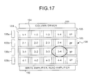
- FIG. 17 is a diagram for explaining a refresh unit in the second embodiment. As shown in FIG. 17, the refresh operation is performed in the unit of sub-array.
- FIG. 17 shows a case in which a sub-array positioned at the fourth place of the block 3 , namely the sub-array of 3 - 4 is a subject of the refresh.
- a refresh operation is accomplished at an interval of 1 ⁇ 5 of that in the conventional case where the refresh operation is performed in the unit of block.
- an oscillation signal generated in a refresh oscillator 121 is divided by a divider 122 so that the frequency is 5 times higher than that of a conventional signal used for controlling refresh timing.
- row addresses for activating a sub-array which is a subject of the refresh are generated successively by the internal address generating circuit 103 and the refresh operation is performed based on the generated row address in the same manner as in the first embodiment.
- FIG. 18 is a circuit diagram showing the essential part of the relation of the connection between the sense amplifiers and the data buses.
- WDB and/WDB are a pair of data buses
- CL is a column selective line used when the usual data write operation is performed
- RWDB and/RWDB are a pair of data buses used when an operation of rewrite of the data from the data register 104 is performed
- RCL is a column selective line used when the operation of rewrite of the data from the data register 104 is performed.
- the semiconductor memory according to the second embodiment provided with the two data buses RWDB and/RWDB for data rewrite operation and the column selective line RCL besides the two data buses WDB and/WDB for usual data write operation and the column selective line CL.
- WCL in FIG. 18 is a selective line for selecting sense amplifiers corresponding to a sub-array which is a subject of data write or data rewrite.
- the potential level of this selective line WCL is made to be “H” which is common to the sense amplifier column of the sub-array which is a subject of data write and data rewrite.
- Each sense amplifier 185 is connected to the data bus WDB for usual write through two switching transistors Q 1 and Q 2 and to the data bus/WDB for usual write through two switching transistors Q 3 and Q 4 . Also, each sense amplifier 185 is connected to the data bus RWDB for rewrite through two switching transistors Q 5 and Q 6 and to the data bus/RWDB for rewrite through two switching transistors Q 7 and Q 8 .
- Four transistors Q 1 , Q 3 , Q 5 and Q 7 are, respectively, put in the ON state when the potential level of the selective line WCL is “H”.
- Two transistors Q 2 and Q 4 are, respectively, put in the ON state when the potential level of the column selective line CL 1 for usual data write operation is “H”. Therefore, a data wdata is supplied to the sense amplifiers 185 , selected since the potential level of the column selective line CL for usual data write operation is changed to “H” when the potential level of the selective line WCL is “H”, from the data input-output circuit 115 through the two data buses WDB and/WDB for usual data write operation.
- the data is written in a corresponding memory cell. This state is shown in the upper half section of FIG. 18 and the flow of the data is shown by the solid one-side arrow.
- two transistors Q 6 and Q 8 are, respectively, put in the ON state when the potential level of the column selective line RCL 2 for data rewrite operation is “H”. Therefore, data is supplied to the sense amplifiers 185 , selected since the potential level of the column selective line RCL 2 for data rewrite operation is changed to “H” when the potential level of the selective line WCL is “H”, from the data register 104 through the two data buses RWDB and/RWDB for data rewrite operation. The data is rewritten in a corresponding memory cell. This state is shown in the lower half section of FIG. 18 and the flow of the data is shown by the one-side arrow of the two-dot long and two short dashes line. The column selective line RCL 2 for data rewrite operation is placed in the “H” level on the basis of the column address held together with the data in the data register 104 .
- Such a structure as to the relation of the connection between the sense amplifiers 185 and the data bus ensures that an operation of writing data in a certain memory cell in response to a write command and an operation of rewriting the held data from the data register 104 in a memory cell having the same column address as the certain memory cell can be performed independently in the sense amplifier column selected when the potential level of the selective line WCL is “H”. Accordingly, the two data buses RWDB and/RWDB for data rewrite operation, the column selective line RCL for data rewrite operation and the switching transistors Q 6 and Q 8 constitute a means for rewriting the data stored and held in the data register 104 in a corresponding memory cell.
- FIG. 19 is a waveform chart showing a waveform of each signal when data is written in a certain memory cell and data is rewritten in a memory cell having the same row address as the certain memory cell from the data register 104 in the circuit shown in FIG. 18 .
- WRT represents a timing signal for write
- WL represents the potential of a word line
- CL represents the potential of the column selective line CL for usual data write operation
- RCL represents the potential of the column selective line RCL for data rewrite operation
- BL and/BL respectively represent the potential of bit lines.
- the block 2 is a subject of the data read. For this reason, five sub-arrays 2 - 1 , 2 - 2 , 2 - 3 , 2 - 4 and 2 P belonging to the block 2 are activated. The data and the parity are output from a memory cell in each of these five sub-arrays.
- the block 2 is a subject of data the read.
- the column address held in the data register coincides with the column address which is a subject of the read and effective data which is to be written in a memory cell which is a subject of the read in the sub-array 2 - 4 is held in the data register 105 b .
- the data and the parity are output from a corresponding memory cell, but no correct data is output from the sub-array 2 - 4 .
- correct data is output from the data register 105 b through a logical circuit 201 .
- This logical circuit 201 will be explained later.
- the data held in the data register 105 b is rewritten in a corresponding memory cell of the sub-array 2 - 4 .
- the data held in the data register 105 b is invalid resulting from the completion of rewrite of the held data and therefore a corresponding flag of the data register 105 b becomes 0.
- the same usual read operation as in FIG. 20 is carried out and the data in the data register is rewritten.
- FIG. 22 is a circuit diagram showing one example of the structure of the logical circuit 201 .
- This logical circuit 201 comprises transfer gates and inverters in numbers respectively equal to the number of sub-arrays per one block, specifically, five transfer gates Tr 5 to Tr 9 and five inverters In 15 to In 19 in the example illustrated.
- seg 0 z to seg 4 z are segment numbers of the data in the direction of the column of the sub-array which data is held in the data register corresponding to each address and rega 01 is data held in the data register corresponding to a row address of a 01 .
- rcdbpz is a read common data bus corresponding to the sub-array with a parity and rcdb 0 z to rcdb 3 z are read common data buses corresponding to four sub-arrays excluding the sub-array with a parity in one block.
- These read common data buses rcdbpz and rcdb 0 z to rcdb 3 z are used in common with the data buses for usual read data.
- the potential level of each of seg 0 z to seg 4 z is “H” when it is selected and “L” when it is unselected.
- the transfer gate Tr 5 is controlled by the signal seg 0 z and a signal obtained by inverting the signal seg 0 z by the inverter In 15 and is put in the ON state when the potential level of seg 0 z is “H”.
- the transfer gate Tr 6 is controlled by the signal seg 1 z and a signal obtained by inverting the signal seg 1 z by the inverter In 16 and is put in the ON state when the potential level of seg 1 z is “H”.
- the transfer gate Tr 7 , the transfer gate Tr 8 and the transfer gate Tr 9 are put in the ON state when the potential of each of seg 2 z, seg 3 z and seg 4 z is “H”, respectively.
- the data rega 01 held in the data register is output to desired read common data buses rcdbpz and rcdb 0 z to rcdb 3 z.
- the block 2 is a subject of the data read similarly to the case of FIG. 20 and the sub-array of 3 - 4 is a subject of the refresh.
- the refresh operation is given priority, a word line corresponding to the sub-array of 3 - 4 is activated, but a word line for the sub-array of 2 - 4 is not activated. Therefore, the data stored in a memory cell in the sub-array 2 - 4 is not output.
- the data of the sub-array of 2 - 4 is assumed as 1 to generate a parity on the basis of the above data and the data read from three sub-arrays 2 - 1 , 2 - 2 and 2 - 3 . Then, the generated parity is compared with the parity read from the sub-array of 2 P in the parity-data comparing circuit 107 to thereby determine the value of the data to be read from the sub-array of 2 - 4 .
- the block 2 is a subject of the data read similarly to the case of FIG. 20 and the sub-array of 3 - 4 is a subject of the refresh.
- the data register 105 b stores effective data to be originally stored in the sub-array 2 - 2 and the column address held in the data register does not coincide with the column address which is a subject of the read.
- the data read operation is the same as when the refresh operation and the data read operation are performed at the same time and the flag of the data register 104 is 0 (the case shown in FIG. 23 ). Then, since the flag of the data register 104 is 1 , corresponding data from the data register 105 b is rewritten in a proper memory cell and a corresponding flag is set to 0.
- the data held in the register is output as correct data to the parity-data comparing circuit 107 in the same manner as in the case of FIG. 21 .
- the block 2 is a subject of the data write. For this reason, five sub-arrays 2 - 1 , 2 - 2 , 2 - 3 , 2 - 4 and 2 P belonging to the block 2 are activated. The data and the parity are written in a memory cell in each of these five sub-arrays. When the flag is 0, for example, an operation of rewrite of the data from the data register 105 b and an operation of making the data held in the data register 105 b invalid are not performed.
- the block 2 is a subject of the data write similarly to the case of FIG. 25 and the sub-array of 3 - 4 is a subject of the refresh.
- the sub-array of 2 - 4 and the sub-array of 3 - 4 use the same sense amplifier in common, the sub-array of 3 - 4 which is a subject of the refresh is activated, but the sub-array of 2 - 4 is not activated.
- the block 2 is a subject of the data write and the sub-array of 3 - 3 is a subject of the refresh.
- effective data to be originally stored in the sub-array of 2 - 4 is held in the data register 105 b with a row address corresponding to a memory cell which is a subject of the write.
- the semiconductor memory is freed from refresh without using a cache memory. Therefore, the problem that a difference in the speed of the read operation and in the speed of the write operation caused by the hit or miss of the cache when acache memory is used to free a semiconductor memory from the refresh operation and the problem that the semiconductor memory is large-scaled or the degree of integration is decreased by disposing a large cache memory to lower the rate of cache miss can be solved.
- the semiconductor memory 101 can be used as a storage of an SRAM interface in the same manner as in the first embodiment. Also, the semiconductor memory 101 may be used as a memory device which is the same as or similar to a DRAM interface and for which a refresh command from the outside is not required. Also, according to the second embodiment, the peak current consumption during refresh operation is more decreased than in the conventional case of performing refresh in the unit of block because a refresh operation is performed in the unit of sub-array.
- the number of the blocks defined by a row address is four, as an example.
- the invention is not limited to this case and the number of the blocks may be three or less or five or more.
- all of the structure of the memory cell array 108 , the number of the sense amplifiers, the structure as to the connection between the sense amplifiers and the data buses, the refresh signal generating circuit 102 , the parity generating circuit 106 and the parity-data comparing circuit 107 are not limited to the aforementioned structures and can be variously changed in design.
- the address held in the data register 104 may be compared with the address which is a subject of read or write to determine whether effective data is held in the data register 104 or not.
- the input or output of data to or from the data register 104 maybe controlled by a switching means. Further, the controller is made to store an address corresponding to effective data held in the data register 104 in advance and based on the stored address, whether the effective data is held in the data register 104 or not may be determined.
- the semiconductor memory can be freed from refresh operation apparently without using a cache memory and, therefore, the problem which arises when the refresh operation of a semiconductor memory is freed using the cache memory can be solved.
Abstract
Description
Claims (20)
Applications Claiming Priority (2)
| Application Number | Priority Date | Filing Date | Title |
|---|---|---|---|
| JP2000368423A JP3938842B2 (en) | 2000-12-04 | 2000-12-04 | Semiconductor memory device |
| JP2000-368423 | 2000-12-04 |
Publications (2)
| Publication Number | Publication Date |
|---|---|
| US20020067649A1 US20020067649A1 (en) | 2002-06-06 |
| US6421292B1 true US6421292B1 (en) | 2002-07-16 |
Family
ID=18838663
Family Applications (1)
| Application Number | Title | Priority Date | Filing Date |
|---|---|---|---|
| US09/892,748 Expired - Lifetime US6421292B1 (en) | 2000-12-04 | 2001-06-28 | Semiconductor memory, and memory access method |
Country Status (6)
| Country | Link |
|---|---|
| US (1) | US6421292B1 (en) |
| EP (1) | EP1215678A3 (en) |
| JP (1) | JP3938842B2 (en) |
| KR (1) | KR100664477B1 (en) |
| CN (1) | CN1226749C (en) |
| TW (1) | TW512343B (en) |
Cited By (10)
| Publication number | Priority date | Publication date | Assignee | Title |
|---|---|---|---|---|
| US20020156967A1 (en) * | 2001-04-18 | 2002-10-24 | Fujitsu Limited | Semiconductor memory device |
| US6535452B2 (en) * | 2001-07-09 | 2003-03-18 | Fujitsu Limited | Semiconductor memory device having error correction function for data reading during refresh operation |
| EP1657723A1 (en) * | 2003-08-18 | 2006-05-17 | Fujitsu Limited | Semiconductor memory and operation method of semiconductor memory |
| US20060291314A1 (en) * | 2005-06-23 | 2006-12-28 | Sanyo Electric Co., Ltd. | Memory |
| US20070025172A1 (en) * | 2005-07-28 | 2007-02-01 | Sanyo Electric Co., Ltd. | Memory |
| US20070147127A1 (en) * | 2005-12-26 | 2007-06-28 | Ching-Yuan Lin | Nonvolatile memory device having self reprogramming function |
| US20080192546A1 (en) * | 2000-02-17 | 2008-08-14 | Conley Kevin M | Flash EEprom System With Simultaneous Multiple Data Sector Programming and Storage of Physical Block Characteristics in Other Designated Blocks |
| US8582383B2 (en) | 2010-04-15 | 2013-11-12 | Renesas Electronics Corporation | Semiconductor memory device with hidden refresh and method for controlling the same |
| US8717833B2 (en) * | 2004-12-15 | 2014-05-06 | Spansion Llc | Semiconductor memory device having non-volatile memory circuits in single chip |
| US10613931B2 (en) | 2018-01-15 | 2020-04-07 | Samsung Electronics Co., Ltd. | Memory devices |
Families Citing this family (12)
| Publication number | Priority date | Publication date | Assignee | Title |
|---|---|---|---|---|
| JP4712214B2 (en) * | 2001-04-09 | 2011-06-29 | 富士通セミコンダクター株式会社 | Semiconductor memory operation control method and semiconductor memory |
| JP4768163B2 (en) * | 2001-08-03 | 2011-09-07 | 富士通セミコンダクター株式会社 | Semiconductor memory |
| KR100481820B1 (en) * | 2002-09-26 | 2005-04-11 | (주)실리콘세븐 | SRAM comPatible Memory Device comPensating an outPut data with Parity and OPerating Method thereof |
| CN100433195C (en) * | 2003-12-31 | 2008-11-12 | 深圳市朗科科技股份有限公司 | Flash memory medium data writing method |
| JP4093197B2 (en) * | 2004-03-23 | 2008-06-04 | セイコーエプソン株式会社 | Display driver and electronic device |
| JP4273087B2 (en) * | 2005-02-08 | 2009-06-03 | エルピーダメモリ株式会社 | Semiconductor memory device and writing method thereof |
| US8161356B2 (en) | 2008-03-28 | 2012-04-17 | Intel Corporation | Systems, methods, and apparatuses to save memory self-refresh power |
| WO2010150054A1 (en) * | 2009-06-25 | 2010-12-29 | St-Ericsson (Grenoble) Sas | Autonomous control of a memory. |
| US9003153B2 (en) * | 2010-11-08 | 2015-04-07 | Greenliant Llc | Method of storing blocks of data in a plurality of memory devices in a redundant manner, a memory controller and a memory system |
| US10380024B2 (en) * | 2017-12-05 | 2019-08-13 | Nanya Technology Corporation | DRAM and method of operating the same in an hierarchical memory system |
| US10503670B2 (en) * | 2017-12-21 | 2019-12-10 | Advanced Micro Devices, Inc. | Dynamic per-bank and all-bank refresh |
| US11681465B2 (en) | 2020-06-12 | 2023-06-20 | Advanced Micro Devices, Inc. | Dynamic multi-bank memory command coalescing |
Citations (3)
| Publication number | Priority date | Publication date | Assignee | Title |
|---|---|---|---|---|
| US5184325A (en) * | 1989-03-10 | 1993-02-02 | Board Of Regents, The University Of Texas System | Dynamic associative memory with logic-in-refresh |
| US5469555A (en) * | 1991-12-19 | 1995-11-21 | Opti, Inc. | Adaptive write-back method and apparatus wherein the cache system operates in a combination of write-back and write-through modes for a cache-based microprocessor system |
| US5999474A (en) | 1998-10-01 | 1999-12-07 | Monolithic System Tech Inc | Method and apparatus for complete hiding of the refresh of a semiconductor memory |
Family Cites Families (3)
| Publication number | Priority date | Publication date | Assignee | Title |
|---|---|---|---|---|
| JPH0612613B2 (en) * | 1986-03-18 | 1994-02-16 | 富士通株式会社 | Semiconductor memory device |
| US6108229A (en) * | 1996-05-24 | 2000-08-22 | Shau; Jeng-Jye | High performance embedded semiconductor memory device with multiple dimension first-level bit-lines |
| US6075740A (en) * | 1998-10-27 | 2000-06-13 | Monolithic System Technology, Inc. | Method and apparatus for increasing the time available for refresh for 1-t SRAM compatible devices |
-
2000
- 2000-12-04 JP JP2000368423A patent/JP3938842B2/en not_active Expired - Fee Related
-
2001
- 2001-06-27 TW TW90115578A patent/TW512343B/en not_active IP Right Cessation
- 2001-06-28 US US09/892,748 patent/US6421292B1/en not_active Expired - Lifetime
- 2001-06-29 KR KR20010038290A patent/KR100664477B1/en not_active IP Right Cessation
- 2001-07-09 EP EP20010305891 patent/EP1215678A3/en not_active Withdrawn
- 2001-08-23 CN CNB011257261A patent/CN1226749C/en not_active Expired - Fee Related
Patent Citations (3)
| Publication number | Priority date | Publication date | Assignee | Title |
|---|---|---|---|---|
| US5184325A (en) * | 1989-03-10 | 1993-02-02 | Board Of Regents, The University Of Texas System | Dynamic associative memory with logic-in-refresh |
| US5469555A (en) * | 1991-12-19 | 1995-11-21 | Opti, Inc. | Adaptive write-back method and apparatus wherein the cache system operates in a combination of write-back and write-through modes for a cache-based microprocessor system |
| US5999474A (en) | 1998-10-01 | 1999-12-07 | Monolithic System Tech Inc | Method and apparatus for complete hiding of the refresh of a semiconductor memory |
Non-Patent Citations (1)
| Title |
|---|
| Nogami et al. "1-Mbit Virtually Static RAM," IEEE Journal of Solid-State Circuits, vol. SC-21, No. 5, Oct. 1996, pp. 662-667. |
Cited By (27)
| Publication number | Priority date | Publication date | Assignee | Title |
|---|---|---|---|---|
| US7889554B2 (en) | 2000-02-17 | 2011-02-15 | Sandisk Corporation | Flash EEPROM system with simultaneous multiple data sector programming and storage of physical block characteristics in other designated blocks |
| US20080192546A1 (en) * | 2000-02-17 | 2008-08-14 | Conley Kevin M | Flash EEprom System With Simultaneous Multiple Data Sector Programming and Storage of Physical Block Characteristics in Other Designated Blocks |
| US7532511B2 (en) * | 2000-02-17 | 2009-05-12 | Sandisk Corporation | Flash EEPROM system with simultaneous multiple data sector programming and storage of physical block characteristics in other designated blocks |
| US20090175080A1 (en) * | 2000-02-17 | 2009-07-09 | Conley Kevin M | Flash EEprom System With Simultaneous Multiple Data Sector Programming and Storage of Physical Block Characteristics in Other Designated Blocks |
| US8797798B2 (en) | 2000-02-17 | 2014-08-05 | Sandisk Corporation | Flash EEPROM system with simultaneous multiple data sector programming and storage of physical block characteristics in other designated blocks |
| US8503240B2 (en) | 2000-02-17 | 2013-08-06 | Sandisk Corporation | Flash EEPROM system with simultaneous multiple data sector programming and storage of physical block characteristics in other designated blocks |
| US20090175082A1 (en) * | 2000-02-17 | 2009-07-09 | Conley Kevin M | Flash EEprom System With Simultaneous Multiple Data Sector Programming and Storage of Physical Block Characteristics in Other Designated Blocks |
| US8223547B2 (en) | 2000-02-17 | 2012-07-17 | Sandisk Corporation | Flash EEprom system with simultaneous multiple data sector programming and storage of physical block characteristics in other designated blocks |
| US7889590B2 (en) | 2000-02-17 | 2011-02-15 | Sandisk Corporation | Flash EEPROM system with simultaneous multiple data sector programming and storage of physical block characteristics in other designated blocks |
| US7646666B2 (en) | 2000-02-17 | 2010-01-12 | Sandisk Corporation | Flash EEPROM system with simultaneous multiple data sector programming and storage of physical block characteristics in other designated blocks |
| US7646667B2 (en) | 2000-02-17 | 2010-01-12 | Sandisk Corporation | Flash EEprom system with simultaneous multiple data sector programming and storage of physical block characteristics in other designated blocks |
| US20100049910A1 (en) * | 2000-02-17 | 2010-02-25 | Conley Kevin M | Flash EEprom System With Simultaneous Multiple Data Sector Programming and Storage of Physical Block Characteristics in Other Designated Blocks |
| US6922750B2 (en) * | 2001-04-18 | 2005-07-26 | Fujitsu Limited | Semiconductor memory device capable of simultaneously reading data and refreshing data |
| US20020156967A1 (en) * | 2001-04-18 | 2002-10-24 | Fujitsu Limited | Semiconductor memory device |
| US6535452B2 (en) * | 2001-07-09 | 2003-03-18 | Fujitsu Limited | Semiconductor memory device having error correction function for data reading during refresh operation |
| EP1657723A4 (en) * | 2003-08-18 | 2007-10-31 | Fujitsu Ltd | Semiconductor memory and operation method of semiconductor memory |
| EP1657723A1 (en) * | 2003-08-18 | 2006-05-17 | Fujitsu Limited | Semiconductor memory and operation method of semiconductor memory |
| US8717833B2 (en) * | 2004-12-15 | 2014-05-06 | Spansion Llc | Semiconductor memory device having non-volatile memory circuits in single chip |
| US7423925B2 (en) * | 2005-06-23 | 2008-09-09 | Sanyo Electric Co., Ltd. | Memory |
| US20060291314A1 (en) * | 2005-06-23 | 2006-12-28 | Sanyo Electric Co., Ltd. | Memory |
| US7362642B2 (en) * | 2005-07-28 | 2008-04-22 | Sanyo Electric Co., Ltd. | Memory |
| CN1905057B (en) * | 2005-07-28 | 2012-02-29 | 帕特兰尼拉财富有限公司 | Memory |
| US20070025172A1 (en) * | 2005-07-28 | 2007-02-01 | Sanyo Electric Co., Ltd. | Memory |
| US7385855B2 (en) * | 2005-12-26 | 2008-06-10 | Ememory Technology Inc. | Nonvolatile memory device having self reprogramming function |
| US20070147127A1 (en) * | 2005-12-26 | 2007-06-28 | Ching-Yuan Lin | Nonvolatile memory device having self reprogramming function |
| US8582383B2 (en) | 2010-04-15 | 2013-11-12 | Renesas Electronics Corporation | Semiconductor memory device with hidden refresh and method for controlling the same |
| US10613931B2 (en) | 2018-01-15 | 2020-04-07 | Samsung Electronics Co., Ltd. | Memory devices |
Also Published As
| Publication number | Publication date |
|---|---|
| CN1226749C (en) | 2005-11-09 |
| US20020067649A1 (en) | 2002-06-06 |
| JP2002170384A (en) | 2002-06-14 |
| JP3938842B2 (en) | 2007-06-27 |
| CN1357891A (en) | 2002-07-10 |
| TW512343B (en) | 2002-12-01 |
| EP1215678A2 (en) | 2002-06-19 |
| KR100664477B1 (en) | 2007-01-04 |
| EP1215678A3 (en) | 2004-01-21 |
| KR20020044045A (en) | 2002-06-14 |
Similar Documents
| Publication | Publication Date | Title |
|---|---|---|
| US6421292B1 (en) | Semiconductor memory, and memory access method | |
| JP4159280B2 (en) | Semiconductor memory device | |
| KR940005684B1 (en) | Semiconductor memory device supporting cache and method of driving the same | |
| TWI534801B (en) | Apparatuses and methods for selective row refreshes | |
| US5659515A (en) | Semiconductor memory device capable of refresh operation in burst mode | |
| KR101213315B1 (en) | Methods, circuits, and systems to select memory regions | |
| JP3280704B2 (en) | Semiconductor storage device | |
| JPH069114B2 (en) | Semiconductor memory | |
| JPH087995B2 (en) | Method and apparatus for refreshing dynamic semiconductor memory device | |
| JPH11176190A (en) | Semiconductor storage and its driving method | |
| US7304908B2 (en) | SRAM device capable of performing burst operation | |
| US5566119A (en) | Synchronous DRAM performing refresh operation a plurality of times in response to each refresh request command | |
| KR100564633B1 (en) | Semiconductor memory device having improved operation performance and access control method of the same | |
| US7508706B2 (en) | Nonvolatile semiconductor memory device provided with data register for temporarily holding data in memory array | |
| US20050105357A1 (en) | Method and circuit configuration for refreshing data in a semiconductor memory | |
| US6510094B2 (en) | Method and apparatus for refreshing semiconductor memory | |
| JP4184036B2 (en) | Semiconductor memory device and test method thereof | |
| US20010015929A1 (en) | Integrated circuit memory devices having multiple input/output buses and precharge circuitry for precharging the input/output buses between write operations | |
| JP4060527B2 (en) | Clock synchronous dynamic memory | |
| JP4900310B2 (en) | Semiconductor memory device | |
| JPH1145570A (en) | Semiconductor memory device | |
| US20230221871A1 (en) | Memory device and operating method thereof | |
| JP3793580B2 (en) | Semiconductor memory device and method for controlling line memory | |
| JP3050901B2 (en) | Semiconductor storage device | |
| JP3238568B2 (en) | Semiconductor storage device |
Legal Events
| Date | Code | Title | Description |
|---|---|---|---|
| AS | Assignment |
Owner name: FUJITSU LIMITED, JAPAN Free format text: ASSIGNMENT OF ASSIGNORS INTEREST;ASSIGNORS:KITAMOTO, AYAKO;MATSUMIYA, MASATO;YAMADA, SHINICHI;AND OTHERS;REEL/FRAME:011943/0772 Effective date: 20010508 |
|
| STCF | Information on status: patent grant |
Free format text: PATENTED CASE |
|
| FEPP | Fee payment procedure |
Free format text: PAYOR NUMBER ASSIGNED (ORIGINAL EVENT CODE: ASPN); ENTITY STATUS OF PATENT OWNER: LARGE ENTITY |
|
| CC | Certificate of correction | ||
| FPAY | Fee payment |
Year of fee payment: 4 |
|
| AS | Assignment |
Owner name: FUJITSU MICROELECTRONICS LIMITED, JAPAN Free format text: ASSIGNMENT OF ASSIGNORS INTEREST;ASSIGNOR:FUJITSU LIMITED;REEL/FRAME:021998/0645 Effective date: 20081104 Owner name: FUJITSU MICROELECTRONICS LIMITED,JAPAN Free format text: ASSIGNMENT OF ASSIGNORS INTEREST;ASSIGNOR:FUJITSU LIMITED;REEL/FRAME:021998/0645 Effective date: 20081104 |
|
| FPAY | Fee payment |
Year of fee payment: 8 |
|
| AS | Assignment |
Owner name: FUJITSU SEMICONDUCTOR LIMITED, JAPAN Free format text: CHANGE OF NAME;ASSIGNOR:FUJITSU MICROELECTRONICS LIMITED;REEL/FRAME:024982/0245 Effective date: 20100401 |
|
| FPAY | Fee payment |
Year of fee payment: 12 |
|
| AS | Assignment |
Owner name: SOCIONEXT INC., JAPAN Free format text: ASSIGNMENT OF ASSIGNORS INTEREST;ASSIGNOR:FUJITSU SEMICONDUCTOR LIMITED;REEL/FRAME:035507/0612 Effective date: 20150302 |