US6428386B1 - Planarizing pads, planarizing machines, and methods for mechanical and/or chemical-mechanical planarization of microelectronic-device substrate assemblies - Google Patents
Planarizing pads, planarizing machines, and methods for mechanical and/or chemical-mechanical planarization of microelectronic-device substrate assemblies Download PDFInfo
- Publication number
- US6428386B1 US6428386B1 US09/595,727 US59572700A US6428386B1 US 6428386 B1 US6428386 B1 US 6428386B1 US 59572700 A US59572700 A US 59572700A US 6428386 B1 US6428386 B1 US 6428386B1
- Authority
- US
- United States
- Prior art keywords
- planarizing
- backing member
- pad
- window
- hole
- Prior art date
- Legal status (The legal status is an assumption and is not a legal conclusion. Google has not performed a legal analysis and makes no representation as to the accuracy of the status listed.)
- Expired - Lifetime
Links
Images


Classifications
-
- B—PERFORMING OPERATIONS; TRANSPORTING
- B24—GRINDING; POLISHING
- B24B—MACHINES, DEVICES, OR PROCESSES FOR GRINDING OR POLISHING; DRESSING OR CONDITIONING OF ABRADING SURFACES; FEEDING OF GRINDING, POLISHING, OR LAPPING AGENTS
- B24B37/00—Lapping machines or devices; Accessories
- B24B37/04—Lapping machines or devices; Accessories designed for working plane surfaces
- B24B37/042—Lapping machines or devices; Accessories designed for working plane surfaces operating processes therefor
-
- B—PERFORMING OPERATIONS; TRANSPORTING
- B24—GRINDING; POLISHING
- B24B—MACHINES, DEVICES, OR PROCESSES FOR GRINDING OR POLISHING; DRESSING OR CONDITIONING OF ABRADING SURFACES; FEEDING OF GRINDING, POLISHING, OR LAPPING AGENTS
- B24B49/00—Measuring or gauging equipment for controlling the feed movement of the grinding tool or work; Arrangements of indicating or measuring equipment, e.g. for indicating the start of the grinding operation
- B24B49/12—Measuring or gauging equipment for controlling the feed movement of the grinding tool or work; Arrangements of indicating or measuring equipment, e.g. for indicating the start of the grinding operation involving optical means
Definitions
- the present invention is directed toward mechanical and/or chemical-mechanical planarization of microelectronic-device substrate assemblies. More specifically, the invention is related to planarizing pads, planarizing machines and methods for optically monitoring the status of a microelectronic-device substrate assembly during a planarizing cycle.
- FIG. 1 schematically illustrates a rotary CMP machine 10 with a platen 20 , a carrier assembly 30 , and a planarizing pad 40 .
- the CMP machine 10 may also have an under-pad 25 attached to an upper surface 22 of the platen 20 and the lower surface of the planarizing pad 40 .
- a drive assembly 26 rotates the platen 20 (indicated by arrow F), or it reciprocates the platen 20 back and forth (indicated by arrow G). Since the planarizing pad 40 is attached to the under-pad 25 , the planarizing pad 40 moves with the platen 20 during planarization.
- the carrier assembly 30 has a head 32 to which a substrate 12 may be attached, or the substrate 12 may be attached to a resilient pad 34 positioned between the substrate 12 and the head 32 .
- the head 32 may be a free-floating wafer carrier, or the head 32 may be coupled to an actuator assembly 36 that imparts axial and/or rotational motion to the substrate 12 (indicated by arrows H and I, respectively).
- the planarizing pad 40 and the planarizing solution 44 define a planarizing medium that mechanically and/or chemically-mechanically removes material from the surface of the substrate
- the planarizing pad 40 can be a fixed-abrasive planarizing pad in which abrasive particles are fixedly bonded to a suspension material.
- the planarizing solution is typically a non-abrasive “clean solution” without abrasive particles.
- the planarizing pad 40 can be a non-abrasive pad composed of a polymeric material (e.g., polyurethane), resin, felt or other suitable non-abrasive materials.
- the planarizing solutions 44 used with the non-abrasive planarizing pads are typically abrasive slurries with abrasive particles suspended in a liquid.
- the carrier assembly 30 presses the substrate 12 face-downward against the polishing medium. More specifically, the carrier assembly 30 generally presses the substrate 12 against the planarizing liquid 44 on the planarizing surface 42 of the planarizing pad 40 , and the platen 20 and/or the carrier assembly 30 move to rub the substrate 12 against the planarizing surface 42 . As the substrate 12 rubs against the planarizing surface 42 , material is removed from the face of the substrate 12 .
- CMP processes should consistently and accurately produce a uniformly planar surface on the substrate to enable precise fabrication of circuits and photo-patterns.
- substrates develop large “step heights” that create highly topographic surfaces.
- Such highly topographical surfaces can impair the accuracy of subsequent photolithographic procedures and other processes that are necessary for forming sub-micron features.
- it is difficult to accurately focus photo patterns to within tolerances approaching 0.1 micron on topographic surfaces because sub-micron photolithographic equipment generally has a very limited depth of field.
- CMP processes are often used to transform a topographical surface into a highly uniform, planar surface at various stages of manufacturing microelectronic devices on a substrate.
- the throughput of CMP processing is a function, at least in part, of the ability to accurately stop CMP processing at a desired endpoint.
- the desired endpoint is reached when the surface of the substrate is planar and/or when enough material has been removed from the substrate to form discrete components on the substrate (e.g., shallow trench isolation areas, contacts and damascene lines).
- the planarizing period of a particular substrate is determined using an estimated polishing rate based upon the polishing rate of identical substrates that were planarized under the same conditions.
- the estimated planarizing period for a particular substrate may not be accurate because the polishing rate or other variables may change from one sabstrate to another. Thus, this method may not produce accurate results.
- the substrate is removed from the pad and then a measuring device measures a change in thickness of the substrate. Removing the substrate from the pad, however, interrupts the planarizing process and may damage the substrate. Thus, this method generally reduces the throughput of CMP processing.
- U.S. Pat. No. 5,433,651 issued to Lustig et al. (“Lustig”) discloses an in-situ chemical-mechanical polishing machine for monitoring the polishing process during a planarizing cycle.
- the polishing machine has a rotatable polishing table including a window embedded in the table.
- a planarizing pad is attached to the table, and the pad has an aperture aligned with the window in the table.
- the window is positioned at a location over which the workpiece can pass for in-situ viewing of a polishing surface of the workpiece from beneath the polishing table.
- the planarizing machine also includes a device for measuring a reflectance signal representative of an in-situ reflectance of the polishing surface of the workpiece.
- slurry may seep under the pad adjacent to the aperture.
- the slurry may accordingly contaminate the backside of the pad or the platen in a manner that affects the consistency of the planarizing process, reduces the life of the pad, and increases maintenance for cleaning.
- Another oral endpointing system is a component of the Mirra® planarizing machine manufactured by Applied Material Corporation of California.
- the Mirra® machine has a rotary platen with an optical emitter/sensor and a planarizing pad with a window over the optical emitter/sensor.
- the planarizing solution can leak through the interface between the pad and the window.
- the Mirra® machine therefore, may also produce inconsistent results, require more maintenance because the backside of the pad and the platen may be contaminated, and reduce the life of the pad because the abrasive particles can wear away the backside of the pad.
- the present invention is directed toward planarizing pads, planarizing machines and methods for manufacturing and using planarizing pads in mechanical and/or chemical-mechanical planarization of microelectronic-device substrate assemblies.
- the machine includes a table having a support surface and an optical monitoring system coupled to the table.
- the table for example, can be a rotary platen or a stationary support surface having an opening at an illumination site.
- the optical monitoring system can have a light source and an optical sensor aligned with the opening in the table to direct and detect a light beam through the opening.
- the planarizing machine can further include a planarizing pad coupled to the support surface of the table.
- the planarizing pad comprises a planarizing medium, an optically transmissive window in the planarizing medium, and a backing member attached to the planarizing medium.
- the planarizing medium can have a planarizing surface, a backside opposite the planarizing surface, and at least one hole extending from the planarizing surface to the backside.
- the hole in the planarizing medium generally has a sidewall transverse to the backside.
- the backing member has a top surface attached to the backside of the planarizing medium and an exposed section extending from the sidewall to either (a) span completely across the hole or (b) project across a portion of the hole for a cover distance that is measured normal to the sidewall.
- the optically transmissive window is positioned in the hole, and it has an interface surface contacting the exposed section o backing member.
- the interface surface of the window generally contacts the exposed section along a seal path that either spans completely across the hole or extends along a length greater than the cover distance.
- the planarizing machine can further include a carrier assembly having a head and a drive mechanism.
- a planarizing solution is disposed on the planarizing surface of the planarizing medium, and then either the head of the carrier system and/or the planarizing pad move in a planarizing plane to rub the substrate against the planarizing medium.
- the optically transmissive window and the backing member are configured to inhibit or eliminate the planarizing solution from leaking through the planarizing pad.
- the optically transmissive window and the backing member are generally discrete components comprising different materials to take advantage of particular optical, and planarizing properties of the window and to also take advantage of the durability and other properties of the backing member.
- FIG. 1 is a schematic cross-sectional view of a rotary planarizing machine in accordance with the prior art.
- FIG. 2A is a schematic cross-sectional view of a rotary planarizing machine and a planarizing pad in accordance with an embodiment of the invention.
- FIG. 2B is a schematic cross-sectional view of a portion of the planarizing machine and the planarizing pad of FIG. 2 A.
- FIG. 3 is a partially schematic cross-sectional view of a planarizing pad similar to the planarizing pad used in the Mirra® planarizing system.
- FIG. 4 is a partially schematic cross-sectional view of a planarizing machine and another planarizing pad in accordance with another embodiment of the invention.
- FIG. 5 is a partially schematic cross-sectional view of another planarizing machine and another planarizing pad in accordance with another embodiment of the invention.
- FIG. 6 is a partially schematic isometric view of a web-format planarizing machine in accordance with an embodiment of the invention.
- the present invention is directed toward planarizing pads, planarizing machines, and methods for optically monitoring mechanical and/or chemical-mechanical planarization of microelectronic-device substrates.
- substrate and “substrate assembly” include semiconductor wafers, field emission displays and other substrate-like structures either before or after forming components on the microelectronic devices.
- substrate assembly includes semiconductor wafers, field emission displays and other substrate-like structures either before or after forming components on the microelectronic devices.
- Many specific details of the invention are described below with reference to rotary planarizing applications to provide a thorough understanding of such embodiments.
- the present invention can be practiced using web-format planarizing machines. A person skilled in the art will thus understand that the invention may have additional embodiments, or that the invention may be practiced without several of the details described below.
- FIG. 2A is a schematic cross-sectional view of a planarizing machine 100 and a planarizing pad 150 in accordance with one embodiment of the invention.
- the planarizing machine 100 of this embodiment also includes a table or platen 120 coupled to a drive mechanism 121 that rotates the platen 120 .
- the platen 120 can include a cavity 122 having an opening 123 at a support surface 124 of the platen 120 .
- An optical monitoring system 127 is attached to the platen 120 in the cavity 122 .
- the optical monitoring system 127 can include an optical emitter/receiver 128 that projects a light to beam 129 through the opening 123 .
- the optical emitter/sensor 128 can be a reflectance device that emits the light beam 129 and senses a reflectance to determine the surface condition of the substrate 12 in-situ and in real time. Reflectance and interferometer endpoint sensors that may be suitable for the optical emitter/sensor 108 are disclosed in U.S. Pat. Nos.
- the planarizing machine 100 can also include a carrier assembly 130 30 having a head 132 coupled to a drive mechanism 136 .
- the head 132 holds and controls a substrate assembly 12 during a planarizing cycle.
- the head 132 can also include a number of nozzles 133 for dispensing a planarizing solution 140 onto the planarizing pad 150 .
- the carrier assembly 130 can be substantially the same as the carrier assembly 30 described above with reference to FIG. 1 .
- the planarizing pad 150 in this embodiment has a planarizing medium 160 , a backing member 170 , and a lens or optically transmissive window 180 .
- the planarizing medium 160 can be an abrasive or a non-abrasive body having a planarizing surface 162 and a backside 164 .
- an abrasive planarizing medium 160 can have a resin binder and a plurality of abrasive particles fixedly attached to the resin binder.
- Suitable abrasive planarizing mediums 151 are disclosed in U.S. Pat. Nos. 5,645,471; 5,879,222; and 5,624,303; and U.S. patent application Ser. Nos. 09/164,916 and 09/001,333; all of which are herein incorporated in their entirety by reference.
- the backing member 170 is an optically transmissive sheet having a top surface 172 and a bottom surface 174 .
- the top surface 172 is adhered to the backside 164 of the planarizing medium 160
- the bottom surface 174 is adhered to the support surface 124 of the platen 120 .
- the backing member 170 can be a continuous sheet of polyester (e.g., optically transmissive Mylar®) or polycarbonate (e.g., Lexan®).
- the backing member 170 in this embodiment preferably transmits a sufficient amount of the light beam 129 to the window 180 .
- the planarizing medium 151 is an abrasive material having fixed-abrasive particles and the backing member 170 is a continuous sheet of optically transmissive Lexan®.
- FIG. 2B is a partial schematic cross-sectional view further illustrating the planarizing pad 150 in greater detail.
- the planarizing medium 160 further includes a hole 166 defined by sidewalls extending transversely to the backside 162 and the planarizing surface 164 .
- the term “transverse” includes all non-parallel configurations and is not limited to perpendicular arrangements.
- the hole 166 can be a circular hole having a diameter D less than 10.0 mm, and more preferably less than approximately 2 mm.
- the window 180 also preferably abuts the sidewalls of the hole 166 .
- the window 180 also 30 preferably has an interface or contact surface 182 coplanar with the backside 162 of the planarizing medium 160 and a top surface 184 coplanar with the planarizing surface 164 .
- the backing member 170 has an exposed section 175 that extends from the sidewall of the hole 166 and preferably spans completely across the hole 166 under the contact surface 182 of the window 180 .
- the window 180 can be attached to the backing member 170 by an adhesive along a seal path defined by the interface between the exposed section 175 of the backing member 170 and the contact surface 182 of the window 180 .
- the backing member 170 and the window 180 are preferably selected to provide the desired optical planarizing properties, planarizing characteristics, and durability.
- the backing member 170 and the window 180 are thus separate, discrete components comprising optically transmissive materials.
- the backing member 170 can comprise a highly durable material having (a) a desired hardness/compressibility to act as a typical backing pad and (b) the desired optical properties so that the light beam 129 can pass through the backing member 170 .
- the window 180 is preferably selected to have good optical properties and a top surface 184 that does not impact the characteristics of the planarizing surface 164 .
- the window 180 for example, can comprise glass, acrylic, clear polycarbonate or other suitable materials.
- the window 180 can comprise a diamond pane that resists scratching so that abrasive particles in the planarizing solution do not alter the optical properties of the window 180 .
- the embodiment of the planarizing pad 150 illustrated in FIGS. 2A and 2B is expected to enhance the flexibility in designing planarizing pads with windows to meet the needs of particular CMP applications.
- One feature of this embodiment of the planarizing pad 150 is that the backing member 170 and the window 180 are discrete components that can be made from different materials. As such, the backing member 170 can be selected to meet the requirements of typical backing pads, and the window 180 can be selected to meet separate optical and planarizing requirements. The particular materials of the backing member 170 and the window 180 can accordingly be selected to optimize the planarizing pad 150 for particular planarizing applications.
- planarizing pad 150 shown in FIGS. 2A and 2B is also expected to reduce or even eliminate leaks that allow the planarizing solution to get underneath the planarizing pad 150 .
- the planarizing solution can seep between the window 180 and the sidewalls of the hole 166 , but the backing member 170 prevents the planarizing solution from leaking onto the platen 120 because it provides a continuous barrier that is impervious to the planarizing solution.
- This is expected to provide a substantial improvement in resisting leaks compared to conventional planarizing pads with windows, such as the planarizing pad 50 shown in FIG. 3 . More particularly, the conventional planarizing pad 50 shown in FIG.
- planarizing medium 60 has a planarizing medium 60 , a backing member 70 with an optical hole 72 , and a window 80 having contact surfaces 82 attached to a small section of the backing member 70 by an adhesive 90 .
- the conventional planarizing pad 50 shown in FIG. 3 is subject to leaking because the planarizing solution can seep through the adhesive 90 and flow through the backing member 170 (shown by the broken-line arrows P-P).
- the planarizing pad 150 shown in FIG. 2B is not susceptible to such leaking because the backing member 170 spans completely across the hole 166 in the planarizing medium 160 , and thus it is expected to prevent the planarizing solution from flowing onto the platen 120 .
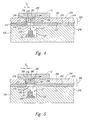
- FIG. 4 is a schematic cross-sectional view of a planarizing pad 250 on the platen 120 in accordance with another embodiment of the invention.
- the planarizing pad 250 has a planarizing medium 260 with a backside 262 , a planarizing surface 264 , and a hole 266 that can be substantially similar to the planarizing medium 160 described above.
- the planarizing pad 250 also includes a backing member 270 having a top surface 272 adhered to the backside 262 of the planarizing medium 260 , and a bottom surface 274 adhered to the platen 120 .
- the backing member 270 can further include a number of exposed sections or lateral sections 275 extending from the sidewalls of the hole 266 to project across a portion of the hole 266 by a cover distance DC measured normal to the sidewalls of the hole 266 .
- each exposed section 275 has a first segment 277 and a second segment 278 that together define an upper surface 276 .
- the second segment 278 generally projects away from the first section 277 at an angle.
- the second segment 278 of the exposed section 275 for example, can define a lip 279 projecting normal to the first segment 277 .
- the exposed sections 275 are separated by an opening in the backing member 270 .
- the opening 273 is aligned with the optical emitter/sensor 128 to allow a 30 light beam 129 to pass through the backing member 270 . Therefore, the backing member 270 can comprise an opaque sheet or other materials that have limited optical transmitivity because these 273 provides an optical pathway for the light beam 129 to pass through the backing member 270 . Suitable opaque materials include foamed polyurethane or other compressible foams, but in other embodiments the backing member 270 can comprise optically transmissive materials or generally incompressible materials.
- the window 280 of the planarizing pad 250 can include a channel 285 configured to receive the second segment 278 of the exposed sections 275 .
- the window 280 accordingly contacts the exposed sections 275 of the backing member 270 along an interface surface to define a seal path between the window 280 and the backing member 270 .
- the seal path has a length greater than the cover distance D, because the interface between the lip 279 and the channel 285 increases the surface area that the window 280 contacts the backing member 270 .
- the window 280 is accordingly adhered to the backing pad 270 along a non-planar, tortuous seal path to prevent or at least inhibit planarizing fluid (not shown) from leaking through the planarizing pad 250 .
- FIG. 5 is a partial schematic cross-sectional view of another embodiment of the planarizing pad 250 in which the first and second segments 277 and 278 of the exposed sections 275 are separate ridges that mate with grooves 286 in the bottom of the window 280 .
- the window 280 can accordingly be attached to the backing member 270 by an adhesive applied to the first and second segments 277 and 278 of the exposed sections 275 .
- the other features of the embodiment of the planarizing pad 250 shown in FIG. 5 are the same as shown in FIG. 4 .
- the window 280 in FIG. 5 is also adhered to the backing member 270 along a non-planar, tortuous seal path.
- planarizing pad 250 illustrated in FIGS. 4 and 5 are expected to reduce leaking of planarizing solution compared to the conventional planarizing pad 50 illustrated in FIG. 3 .
- the planarizing pad 250 is expected to inhibit or eliminate the planarizing solution from leaking onto the platen because the seal path between the window 280 and the backing member 270 is a tortuous path having a length greater than the cover distance D c .
- the planarizing solution must not only pass through more adhesive in the planarizing pad 250 than the planarizing pad 50 , but the planarizing solution must also travel through a torturous path in the planarizing pad 250 that further inhibits the planarizing solution from leaking through the planarizing pad 250 .
- the planarizing pad 250 also provides enhanced design flexibility because the backing member 270 can be made from materials that have a desired compressibility or other properties without necessarily being an optically transmissive material. Therefore, the planarizing pad 250 is expected to be suitable for applications that require particular properties that are not available in optically transmissive materials.
- FIG. 6 is a partially schematic isometric view of a web-format planarizing machine 300 in accordance with another embodiment of the invention.
- the planarizing machine 300 has a support table 302 with a top panel 304 at a work station where an operative portion of a web-format planarizing pad 350 is positioned.
- the top panel 304 is generally a rigid plate that provides a flat, solid surface to which a particular section of the planarizing pad 350 may be secured during planarization.
- the planarizing machine 300 also has a plurality of rollers to guide, position and hold the planarizing pad 350 over the top panel 304 .
- the rollers can include a supply roller 320 , idler rollers 321 , guide rollers 322 , and a take-up roller 323 .
- the supply roller 320 carries an unused or pre-operative portion of the planarizing pad 350
- a take-up roller 323 carries a used or post-operative portion of the planarizing pad 350 .
- the left idler roller 321 and the upper guide roller 322 stretch the planarizing pad 350 over the top panel 304 to hold the planarizing pad 350 stationary during operation.
- a motor (not shown) generally drives the take-up roller 323 to sequentially advance the planarizing pad 350 across the top panel 304 along a pad travel path T—T, and the motor can also drive the supply roller 320 . Accordingly, a clean pre-operative section of the planarizing pad 350 may be quickly substituted for a used section to provide a consistent surface for planarizing and/or cleaning the substrate 12 .
- the web-format planarizing machine 300 also includes a carrier assembly 330 that controls and protects the substrate 12 during planarization.
- the carrier assembly 330 generally has a substrate holder 332 to pick up, hold and release the substrate 12 at appropriate stages of the planarizing cycle. Several nozzles 333 project from the substrate holder 332 to dispense a planarizing solution onto the planarizing pad 350 .
- the carrier assembly 330 also generally has a support gantry 334 carrying a drive assembly 335 that can translate along the gantry 334 .
- the drive assembly 335 generally has an actuator 336 , a drive shaft 337 coupled to the actuator 336 , and an arm 338 projecting from the drive shaft 337 .
- the arm 338 carries the substrate holder 332 via a terminal shaft 339 such that the drive assembly 335 orbits the substrate holder 332 about an axis B—B (arrow R 1 ).
- the terminal shaft 339 may also be coupled to the actuator 336 to rotate the substrate holder 332 about its central axis C—C (arrow R 2 ).
- the planarizing pad 350 shown in FIG. 6 is similar to the planarizing pad 150 shown in FIGS. 2A and 2B.
- the planarizing pad 350 can accordingly include a planarizing medium 360 having a plurality of holes 366 arranged in a line generally parallel to the pad travel path T—T.
- the planarizing pad 350 can also include a plurality of windows 380 in the holes 366 and a backing member 370 under the planarizing medium 360 .
- the planarizing medium 360 , the backing member 370 and the windows 380 can have any of the configurations illustrated above in FIGS. 2B, 4 and 5 .
- the planarizing pad 350 therefore, provides a web-format planarizing pad that prevents the planarizing solution 344 from leaking through the holes 366 .
- the planarizing machine 300 can also include an optical emitter/sensor 128 (shown in the broken lines) attached to the table 302 at an illumination site aligned with the line of windows 380 .
- the carrier assembly 330 preferably lowers the substrate 12 against the planarizing medium 360 and orbits the carrier head 332 about the axis B—B to rub the substrate 12 against the planarizing medium 360 .
- the optical emitter/sensor 128 emits a light beam 129 that passes through a window 380 aligned with the illumination site to optically monitor the status of the substrate 12 during the planarizing cycle.
- the web-format planarizing machine 300 and the planarizing pad 350 are expected to provide the same advantages as the planarizing pads 150 and 250 described above.
- the backing member and window can comprise different materials than those described above to optimize the planarizing pad for the particular optical, planarizing, durability and hardness/compressibility requirements of a particular application. Accordingly, the invention is not limited except as by the appended claims.
Abstract
Description
Claims (62)
Priority Applications (1)
| Application Number | Priority Date | Filing Date | Title |
|---|---|---|---|
| US09/595,727 US6428386B1 (en) | 2000-06-16 | 2000-06-16 | Planarizing pads, planarizing machines, and methods for mechanical and/or chemical-mechanical planarization of microelectronic-device substrate assemblies |
Applications Claiming Priority (1)
| Application Number | Priority Date | Filing Date | Title |
|---|---|---|---|
| US09/595,727 US6428386B1 (en) | 2000-06-16 | 2000-06-16 | Planarizing pads, planarizing machines, and methods for mechanical and/or chemical-mechanical planarization of microelectronic-device substrate assemblies |
Publications (1)
| Publication Number | Publication Date |
|---|---|
| US6428386B1 true US6428386B1 (en) | 2002-08-06 |
Family
ID=24384425
Family Applications (1)
| Application Number | Title | Priority Date | Filing Date |
|---|---|---|---|
| US09/595,727 Expired - Lifetime US6428386B1 (en) | 2000-06-16 | 2000-06-16 | Planarizing pads, planarizing machines, and methods for mechanical and/or chemical-mechanical planarization of microelectronic-device substrate assemblies |
Country Status (1)
| Country | Link |
|---|---|
| US (1) | US6428386B1 (en) |
Cited By (20)
| Publication number | Priority date | Publication date | Assignee | Title |
|---|---|---|---|---|
| US20010053658A1 (en) * | 2000-03-15 | 2001-12-20 | Budinger William D. | Window portion with an adjusted rate of wear |
| US20030148706A1 (en) * | 2002-02-06 | 2003-08-07 | Applied Materials, Inc. | Method and apparatus of eddy current monitoring for chemical mechanical polishing |
| US20030181136A1 (en) * | 2002-03-22 | 2003-09-25 | Billett Bruce H. | CMP pad platen with viewport |
| US20030236055A1 (en) * | 2000-05-19 | 2003-12-25 | Swedek Boguslaw A. | Polishing pad for endpoint detection and related methods |
| US20040198184A1 (en) * | 2001-08-24 | 2004-10-07 | Joslyn Michael J | Planarizing machines and methods for dispensing planarizing solutions in the processing of microelectronic workpieces |
| US20050014457A1 (en) * | 2001-08-24 | 2005-01-20 | Taylor Theodore M. | Apparatus and method for conditioning a contact surface of a processing pad used in processing microelectronic workpieces |
| US20050024040A1 (en) * | 2002-08-29 | 2005-02-03 | Martin Michael H. | Planarity diagnostic system, e.g., for microelectronic component test systems |
| US20050026555A1 (en) * | 2002-08-08 | 2005-02-03 | Terry Castor | Carrier assemblies, planarizing apparatuses including carrier assemblies, and methods for planarizing micro-device workpieces |
| US20060040588A1 (en) * | 1999-04-26 | 2006-02-23 | Elledge Jason B | Apparatus for in-situ optical endpointing on web-format planarizing machines in mechanical or chemical-mechanical planarization of microelectronic-device substrate assemblies and methods for making and using same |
| US20070049179A1 (en) * | 2005-08-31 | 2007-03-01 | Micro Technology, Inc. | Retaining rings, and associated planarizing apparatuses, and related methods for planarizing micro-device workpieces |
| US20070049172A1 (en) * | 2005-08-31 | 2007-03-01 | Micron Technology, Inc. | Apparatus and method for removing material from microfeature workpieces |
| EP2025469A1 (en) | 2003-06-17 | 2009-02-18 | Cabot Microelectronics Corporation | Multi-layer polishing pad material for CMP |
| US20100099339A1 (en) * | 2008-10-16 | 2010-04-22 | Applied Materials, Inc. | Polishing pad edge extension |
| US7708622B2 (en) | 2003-02-11 | 2010-05-04 | Micron Technology, Inc. | Apparatuses and methods for conditioning polishing pads used in polishing micro-device workpieces |
| US7754612B2 (en) | 2007-03-14 | 2010-07-13 | Micron Technology, Inc. | Methods and apparatuses for removing polysilicon from semiconductor workpieces |
| US7854644B2 (en) | 2005-07-13 | 2010-12-21 | Micron Technology, Inc. | Systems and methods for removing microfeature workpiece surface defects |
| US20110244763A1 (en) * | 2010-03-31 | 2011-10-06 | Applied Materials, Inc. | Side pad design for edge pedestal |
| US8105131B2 (en) | 2005-09-01 | 2012-01-31 | Micron Technology, Inc. | Method and apparatus for removing material from microfeature workpieces |
| US9017140B2 (en) | 2010-01-13 | 2015-04-28 | Nexplanar Corporation | CMP pad with local area transparency |
| US9156124B2 (en) | 2010-07-08 | 2015-10-13 | Nexplanar Corporation | Soft polishing pad for polishing a semiconductor substrate |
Citations (44)
| Publication number | Priority date | Publication date | Assignee | Title |
|---|---|---|---|---|
| US4200395A (en) | 1977-05-03 | 1980-04-29 | Massachusetts Institute Of Technology | Alignment of diffraction gratings |
| US4203799A (en) | 1975-05-30 | 1980-05-20 | Hitachi, Ltd. | Method for monitoring thickness of epitaxial growth layer on substrate |
| US4358338A (en) | 1980-05-16 | 1982-11-09 | Varian Associates, Inc. | End point detection method for physical etching process |
| US4367044A (en) | 1980-12-31 | 1983-01-04 | International Business Machines Corp. | Situ rate and depth monitor for silicon etching |
| US4377028A (en) | 1980-02-29 | 1983-03-22 | Telmec Co., Ltd. | Method for registering a mask pattern in a photo-etching apparatus for semiconductor devices |
| US4422764A (en) | 1980-12-12 | 1983-12-27 | The University Of Rochester | Interferometer apparatus for microtopography |
| US4640002A (en) | 1982-02-25 | 1987-02-03 | The University Of Delaware | Method and apparatus for increasing the durability and yield of thin film photovoltaic devices |
| US4660980A (en) | 1983-12-13 | 1987-04-28 | Anritsu Electric Company Limited | Apparatus for measuring thickness of object transparent to light utilizing interferometric method |
| US4717255A (en) | 1986-03-26 | 1988-01-05 | Hommelwerke Gmbh | Device for measuring small distances |
| US4879258A (en) | 1988-08-31 | 1989-11-07 | Texas Instruments Incorporated | Integrated circuit planarization by mechanical polishing |
| US5036015A (en) | 1990-09-24 | 1991-07-30 | Micron Technology, Inc. | Method of endpoint detection during chemical/mechanical planarization of semiconductor wafers |
| US5081796A (en) | 1990-08-06 | 1992-01-21 | Micron Technology, Inc. | Method and apparatus for mechanical planarization and endpoint detection of a semiconductor wafer |
| US5220405A (en) | 1991-12-20 | 1993-06-15 | International Business Machines Corporation | Interferometer for in situ measurement of thin film thickness changes |
| US5324381A (en) | 1992-05-06 | 1994-06-28 | Sumitomo Electric Industries, Ltd. | Semiconductor chip mounting method and apparatus |
| EP0623423A1 (en) | 1993-05-03 | 1994-11-09 | Motorola, Inc. | Method for polishing a substrate |
| US5369488A (en) | 1991-12-10 | 1994-11-29 | Olympus Optical Co., Ltd. | High precision location measuring device wherein a position detector and an interferometer are fixed to a movable holder |
| US5393624A (en) | 1988-07-29 | 1995-02-28 | Tokyo Electron Limited | Method and apparatus for manufacturing a semiconductor device |
| US5413941A (en) | 1994-01-06 | 1995-05-09 | Micron Technology, Inc. | Optical end point detection methods in semiconductor planarizing polishing processes |
| US5433651A (en) * | 1993-12-22 | 1995-07-18 | International Business Machines Corporation | In-situ endpoint detection and process monitoring method and apparatus for chemical-mechanical polishing |
| US5461007A (en) | 1994-06-02 | 1995-10-24 | Motorola, Inc. | Process for polishing and analyzing a layer over a patterned semiconductor substrate |
| US5465154A (en) | 1989-05-05 | 1995-11-07 | Levy; Karl B. | Optical monitoring of growth and etch rate of materials |
| US5609718A (en) | 1995-09-29 | 1997-03-11 | Micron Technology, Inc. | Method and apparatus for measuring a change in the thickness of polishing pads used in chemical-mechanical planarization of semiconductor wafers |
| US5624303A (en) | 1996-01-22 | 1997-04-29 | Micron Technology, Inc. | Polishing pad and a method for making a polishing pad with covalently bonded particles |
| US5645471A (en) | 1995-08-11 | 1997-07-08 | Minnesota Mining And Manufacturing Company | Method of texturing a substrate using an abrasive article having multiple abrasive natures |
| US5667424A (en) | 1996-09-25 | 1997-09-16 | Chartered Semiconductor Manufacturing Pte Ltd. | New chemical mechanical planarization (CMP) end point detection apparatus |
| US5738562A (en) | 1996-01-24 | 1998-04-14 | Micron Technology, Inc. | Apparatus and method for planar end-point detection during chemical-mechanical polishing |
| US5777739A (en) | 1996-02-16 | 1998-07-07 | Micron Technology, Inc. | Endpoint detector and method for measuring a change in wafer thickness in chemical-mechanical polishing of semiconductor wafers |
| US5791969A (en) | 1994-11-01 | 1998-08-11 | Lund; Douglas E. | System and method of automatically polishing semiconductor wafers |
| US5865665A (en) | 1997-02-14 | 1999-02-02 | Yueh; William | In-situ endpoint control apparatus for semiconductor wafer polishing process |
| US5893796A (en) | 1995-03-28 | 1999-04-13 | Applied Materials, Inc. | Forming a transparent window in a polishing pad for a chemical mechanical polishing apparatus |
| US5899792A (en) | 1996-12-10 | 1999-05-04 | Nikon Corporation | Optical polishing apparatus and methods |
| US5934974A (en) | 1997-11-05 | 1999-08-10 | Aplex Group | In-situ monitoring of polishing pad wear |
| US5949927A (en) * | 1992-12-28 | 1999-09-07 | Tang; Wallace T. Y. | In-situ real-time monitoring technique and apparatus for endpoint detection of thin films during chemical/mechanical polishing planarization |
| US5997384A (en) | 1997-12-22 | 1999-12-07 | Micron Technology, Inc. | Method and apparatus for controlling planarizing characteristics in mechanical and chemical-mechanical planarization of microelectronic substrates |
| US6000996A (en) | 1997-02-03 | 1999-12-14 | Dainippon Screen Mfg. Co., Ltd. | Grinding process monitoring system and grinding process monitoring method |
| US6039633A (en) | 1998-10-01 | 2000-03-21 | Micron Technology, Inc. | Method and apparatus for mechanical and chemical-mechanical planarization of microelectronic-device substrate assemblies |
| US6068539A (en) | 1998-03-10 | 2000-05-30 | Lam Research Corporation | Wafer polishing device with movable window |
| US6075606A (en) | 1996-02-16 | 2000-06-13 | Doan; Trung T. | Endpoint detector and method for measuring a change in wafer thickness in chemical-mechanical polishing of semiconductor wafers and other microelectronic substrates |
| US6102775A (en) | 1997-04-18 | 2000-08-15 | Nikon Corporation | Film inspection method |
| US6108091A (en) * | 1997-05-28 | 2000-08-22 | Lam Research Corporation | Method and apparatus for in-situ monitoring of thickness during chemical-mechanical polishing |
| US6108092A (en) * | 1996-05-16 | 2000-08-22 | Micron Technology, Inc. | Method and apparatus for detecting the endpoint in chemical-mechanical polishing of semiconductor wafers |
| US6139402A (en) | 1997-12-30 | 2000-10-31 | Micron Technology, Inc. | Method and apparatus for mechanical and chemical-mechanical planarization of microelectronic substrates |
| US6213845B1 (en) | 1999-04-26 | 2001-04-10 | Micron Technology, Inc. | Apparatus for in-situ optical endpointing on web-format planarizing machines in mechanical or chemical-mechanical planarization of microelectronic-device substrate assemblies and methods for making and using same |
| US6247998B1 (en) | 1999-01-25 | 2001-06-19 | Applied Materials, Inc. | Method and apparatus for determining substrate layer thickness during chemical mechanical polishing |
-
2000
- 2000-06-16 US US09/595,727 patent/US6428386B1/en not_active Expired - Lifetime
Patent Citations (47)
| Publication number | Priority date | Publication date | Assignee | Title |
|---|---|---|---|---|
| US4203799A (en) | 1975-05-30 | 1980-05-20 | Hitachi, Ltd. | Method for monitoring thickness of epitaxial growth layer on substrate |
| US4200395A (en) | 1977-05-03 | 1980-04-29 | Massachusetts Institute Of Technology | Alignment of diffraction gratings |
| US4377028A (en) | 1980-02-29 | 1983-03-22 | Telmec Co., Ltd. | Method for registering a mask pattern in a photo-etching apparatus for semiconductor devices |
| US4358338A (en) | 1980-05-16 | 1982-11-09 | Varian Associates, Inc. | End point detection method for physical etching process |
| US4422764A (en) | 1980-12-12 | 1983-12-27 | The University Of Rochester | Interferometer apparatus for microtopography |
| US4367044A (en) | 1980-12-31 | 1983-01-04 | International Business Machines Corp. | Situ rate and depth monitor for silicon etching |
| US4640002A (en) | 1982-02-25 | 1987-02-03 | The University Of Delaware | Method and apparatus for increasing the durability and yield of thin film photovoltaic devices |
| US4660980A (en) | 1983-12-13 | 1987-04-28 | Anritsu Electric Company Limited | Apparatus for measuring thickness of object transparent to light utilizing interferometric method |
| US4717255A (en) | 1986-03-26 | 1988-01-05 | Hommelwerke Gmbh | Device for measuring small distances |
| US5393624A (en) | 1988-07-29 | 1995-02-28 | Tokyo Electron Limited | Method and apparatus for manufacturing a semiconductor device |
| US4879258A (en) | 1988-08-31 | 1989-11-07 | Texas Instruments Incorporated | Integrated circuit planarization by mechanical polishing |
| US5465154A (en) | 1989-05-05 | 1995-11-07 | Levy; Karl B. | Optical monitoring of growth and etch rate of materials |
| US5081796A (en) | 1990-08-06 | 1992-01-21 | Micron Technology, Inc. | Method and apparatus for mechanical planarization and endpoint detection of a semiconductor wafer |
| US5036015A (en) | 1990-09-24 | 1991-07-30 | Micron Technology, Inc. | Method of endpoint detection during chemical/mechanical planarization of semiconductor wafers |
| US5369488A (en) | 1991-12-10 | 1994-11-29 | Olympus Optical Co., Ltd. | High precision location measuring device wherein a position detector and an interferometer are fixed to a movable holder |
| US5220405A (en) | 1991-12-20 | 1993-06-15 | International Business Machines Corporation | Interferometer for in situ measurement of thin film thickness changes |
| US5324381A (en) | 1992-05-06 | 1994-06-28 | Sumitomo Electric Industries, Ltd. | Semiconductor chip mounting method and apparatus |
| US5949927A (en) * | 1992-12-28 | 1999-09-07 | Tang; Wallace T. Y. | In-situ real-time monitoring technique and apparatus for endpoint detection of thin films during chemical/mechanical polishing planarization |
| EP0623423A1 (en) | 1993-05-03 | 1994-11-09 | Motorola, Inc. | Method for polishing a substrate |
| US5433651A (en) * | 1993-12-22 | 1995-07-18 | International Business Machines Corporation | In-situ endpoint detection and process monitoring method and apparatus for chemical-mechanical polishing |
| US5413941A (en) | 1994-01-06 | 1995-05-09 | Micron Technology, Inc. | Optical end point detection methods in semiconductor planarizing polishing processes |
| US5461007A (en) | 1994-06-02 | 1995-10-24 | Motorola, Inc. | Process for polishing and analyzing a layer over a patterned semiconductor substrate |
| US5791969A (en) | 1994-11-01 | 1998-08-11 | Lund; Douglas E. | System and method of automatically polishing semiconductor wafers |
| US5893796A (en) | 1995-03-28 | 1999-04-13 | Applied Materials, Inc. | Forming a transparent window in a polishing pad for a chemical mechanical polishing apparatus |
| US6045439A (en) * | 1995-03-28 | 2000-04-04 | Applied Materials, Inc. | Forming a transparent window in a polishing pad for a chemical mechanical polishing apparatus |
| US5645471A (en) | 1995-08-11 | 1997-07-08 | Minnesota Mining And Manufacturing Company | Method of texturing a substrate using an abrasive article having multiple abrasive natures |
| US5609718A (en) | 1995-09-29 | 1997-03-11 | Micron Technology, Inc. | Method and apparatus for measuring a change in the thickness of polishing pads used in chemical-mechanical planarization of semiconductor wafers |
| US5624303A (en) | 1996-01-22 | 1997-04-29 | Micron Technology, Inc. | Polishing pad and a method for making a polishing pad with covalently bonded particles |
| US5879222A (en) | 1996-01-22 | 1999-03-09 | Micron Technology, Inc. | Abrasive polishing pad with covalently bonded abrasive particles |
| US5738562A (en) | 1996-01-24 | 1998-04-14 | Micron Technology, Inc. | Apparatus and method for planar end-point detection during chemical-mechanical polishing |
| US6075606A (en) | 1996-02-16 | 2000-06-13 | Doan; Trung T. | Endpoint detector and method for measuring a change in wafer thickness in chemical-mechanical polishing of semiconductor wafers and other microelectronic substrates |
| US5777739A (en) | 1996-02-16 | 1998-07-07 | Micron Technology, Inc. | Endpoint detector and method for measuring a change in wafer thickness in chemical-mechanical polishing of semiconductor wafers |
| US6301006B1 (en) | 1996-02-16 | 2001-10-09 | Micron Technology, Inc. | Endpoint detector and method for measuring a change in wafer thickness |
| US6108092A (en) * | 1996-05-16 | 2000-08-22 | Micron Technology, Inc. | Method and apparatus for detecting the endpoint in chemical-mechanical polishing of semiconductor wafers |
| US5667424A (en) | 1996-09-25 | 1997-09-16 | Chartered Semiconductor Manufacturing Pte Ltd. | New chemical mechanical planarization (CMP) end point detection apparatus |
| US5899792A (en) | 1996-12-10 | 1999-05-04 | Nikon Corporation | Optical polishing apparatus and methods |
| US6000996A (en) | 1997-02-03 | 1999-12-14 | Dainippon Screen Mfg. Co., Ltd. | Grinding process monitoring system and grinding process monitoring method |
| US5865665A (en) | 1997-02-14 | 1999-02-02 | Yueh; William | In-situ endpoint control apparatus for semiconductor wafer polishing process |
| US6102775A (en) | 1997-04-18 | 2000-08-15 | Nikon Corporation | Film inspection method |
| US6108091A (en) * | 1997-05-28 | 2000-08-22 | Lam Research Corporation | Method and apparatus for in-situ monitoring of thickness during chemical-mechanical polishing |
| US5934974A (en) | 1997-11-05 | 1999-08-10 | Aplex Group | In-situ monitoring of polishing pad wear |
| US5997384A (en) | 1997-12-22 | 1999-12-07 | Micron Technology, Inc. | Method and apparatus for controlling planarizing characteristics in mechanical and chemical-mechanical planarization of microelectronic substrates |
| US6139402A (en) | 1997-12-30 | 2000-10-31 | Micron Technology, Inc. | Method and apparatus for mechanical and chemical-mechanical planarization of microelectronic substrates |
| US6068539A (en) | 1998-03-10 | 2000-05-30 | Lam Research Corporation | Wafer polishing device with movable window |
| US6039633A (en) | 1998-10-01 | 2000-03-21 | Micron Technology, Inc. | Method and apparatus for mechanical and chemical-mechanical planarization of microelectronic-device substrate assemblies |
| US6247998B1 (en) | 1999-01-25 | 2001-06-19 | Applied Materials, Inc. | Method and apparatus for determining substrate layer thickness during chemical mechanical polishing |
| US6213845B1 (en) | 1999-04-26 | 2001-04-10 | Micron Technology, Inc. | Apparatus for in-situ optical endpointing on web-format planarizing machines in mechanical or chemical-mechanical planarization of microelectronic-device substrate assemblies and methods for making and using same |
Non-Patent Citations (6)
| Title |
|---|
| Applied Materials, Inc. 2002, "Mira Mesa Advanced Integrated CMP," Applied Materials. Products. CMP. Mirra Mesa CMP, (2 pages). |
| Applied Materials, Inc., 2002, "About the CMP Process, " Applied Materials. Products. CMP. About the CMP Process, (1 page). |
| PCT International Search Report for International Application No. PCT/US99/09016, Aug. 18, 1999, (4 pages). |
| U.S. patent application No. 09/589,380 (Atty Docket No. 108298504US), Agarwal, filed Jun. 7, 2000. |
| U.S. patent application No. 09/651,240 (Atty. Docket No. 1082998522US), Moore, filed Aug. 30, 2000. |
| U.S. patent application No. 09/651,417 (Atty Docket No. 108298534US), Moore, filed Aug. 30, 2000. |
Cited By (45)
| Publication number | Priority date | Publication date | Assignee | Title |
|---|---|---|---|---|
| US20060040588A1 (en) * | 1999-04-26 | 2006-02-23 | Elledge Jason B | Apparatus for in-situ optical endpointing on web-format planarizing machines in mechanical or chemical-mechanical planarization of microelectronic-device substrate assemblies and methods for making and using same |
| US7479206B2 (en) * | 1999-04-26 | 2009-01-20 | Micron Technology, Inc. | Apparatus for in-situ optical endpointing on web-format planarizing machines in mechanical or chemical-mechanical planarization of microelectronic-device substrate assemblies |
| US20010053658A1 (en) * | 2000-03-15 | 2001-12-20 | Budinger William D. | Window portion with an adjusted rate of wear |
| US6860793B2 (en) * | 2000-03-15 | 2005-03-01 | Rohm And Haas Electronic Materials Cmp Holdings, Inc. | Window portion with an adjusted rate of wear |
| US7429207B2 (en) | 2000-05-19 | 2008-09-30 | Applied Materials, Inc. | System for endpoint detection with polishing pad |
| US20070077862A1 (en) * | 2000-05-19 | 2007-04-05 | Applied Materials, Inc. | System for Endpoint Detection with Polishing Pad |
| US20030236055A1 (en) * | 2000-05-19 | 2003-12-25 | Swedek Boguslaw A. | Polishing pad for endpoint detection and related methods |
| US8485862B2 (en) | 2000-05-19 | 2013-07-16 | Applied Materials, Inc. | Polishing pad for endpoint detection and related methods |
| US9333621B2 (en) | 2000-05-19 | 2016-05-10 | Applied Materials, Inc. | Polishing pad for endpoint detection and related methods |
| US7118457B2 (en) | 2000-05-19 | 2006-10-10 | Applied Materials, Inc. | Method of forming a polishing pad for endpoint detection |
| US20050124273A1 (en) * | 2000-05-19 | 2005-06-09 | Applied Materials, Inc., A Delaware Corporation | Method of forming a polishing pad for endpoint detection |
| US20050014457A1 (en) * | 2001-08-24 | 2005-01-20 | Taylor Theodore M. | Apparatus and method for conditioning a contact surface of a processing pad used in processing microelectronic workpieces |
| US20050181712A1 (en) * | 2001-08-24 | 2005-08-18 | Taylor Theodore M. | Apparatus and method for conditioning a contact surface of a processing pad used in processing microelectronic workpieces |
| US20060128279A1 (en) * | 2001-08-24 | 2006-06-15 | Micron Technology, Inc. | Apparatus and method for conditioning a contact surface of a processing pad used in processing microelectronic workpieces |
| US20040198184A1 (en) * | 2001-08-24 | 2004-10-07 | Joslyn Michael J | Planarizing machines and methods for dispensing planarizing solutions in the processing of microelectronic workpieces |
| US20050208884A1 (en) * | 2001-08-24 | 2005-09-22 | Micron Technology, Inc. | Apparatus and method for conditioning a contact surface of a processing pad used in processing microelectronic workpieces |
| US20080064301A1 (en) * | 2002-02-06 | 2008-03-13 | Applied Materials, Inc. | Method and Apparatus Of Eddy Current Monitoring For Chemical Mechanical Polishing |
| US20060025052A1 (en) * | 2002-02-06 | 2006-02-02 | Manoocher Birang | Method and apparatus of eddy current monitoring for chemical mechanical polishing |
| US7001242B2 (en) | 2002-02-06 | 2006-02-21 | Applied Materials, Inc. | Method and apparatus of eddy current monitoring for chemical mechanical polishing |
| US20030148706A1 (en) * | 2002-02-06 | 2003-08-07 | Applied Materials, Inc. | Method and apparatus of eddy current monitoring for chemical mechanical polishing |
| US7374477B2 (en) * | 2002-02-06 | 2008-05-20 | Applied Materials, Inc. | Polishing pads useful for endpoint detection in chemical mechanical polishing |
| US7591708B2 (en) | 2002-02-06 | 2009-09-22 | Applied Materials, Inc. | Method and apparatus of eddy current monitoring for chemical mechanical polishing |
| US20030148721A1 (en) * | 2002-02-06 | 2003-08-07 | Applied Materials, Inc. | Polishing pads useful for endpoint detection in chemical mechanical polishing |
| US20030181136A1 (en) * | 2002-03-22 | 2003-09-25 | Billett Bruce H. | CMP pad platen with viewport |
| US8858298B2 (en) | 2002-07-24 | 2014-10-14 | Applied Materials, Inc. | Polishing pad with two-section window having recess |
| US20050026555A1 (en) * | 2002-08-08 | 2005-02-03 | Terry Castor | Carrier assemblies, planarizing apparatuses including carrier assemblies, and methods for planarizing micro-device workpieces |
| US20070108965A1 (en) * | 2002-08-29 | 2007-05-17 | Micron Technology, Inc. | Planarity diagnostic system, e.g., for microelectronic component test systems |
| US20050024040A1 (en) * | 2002-08-29 | 2005-02-03 | Martin Michael H. | Planarity diagnostic system, e.g., for microelectronic component test systems |
| US20060125471A1 (en) * | 2002-08-29 | 2006-06-15 | Micron Technology, Inc. | Planarity diagnostic system, E.G., for microelectronic component test systems |
| US7708622B2 (en) | 2003-02-11 | 2010-05-04 | Micron Technology, Inc. | Apparatuses and methods for conditioning polishing pads used in polishing micro-device workpieces |
| US7997958B2 (en) | 2003-02-11 | 2011-08-16 | Micron Technology, Inc. | Apparatuses and methods for conditioning polishing pads used in polishing micro-device workpieces |
| EP2025469A1 (en) | 2003-06-17 | 2009-02-18 | Cabot Microelectronics Corporation | Multi-layer polishing pad material for CMP |
| US7854644B2 (en) | 2005-07-13 | 2010-12-21 | Micron Technology, Inc. | Systems and methods for removing microfeature workpiece surface defects |
| US20070049172A1 (en) * | 2005-08-31 | 2007-03-01 | Micron Technology, Inc. | Apparatus and method for removing material from microfeature workpieces |
| US7927181B2 (en) | 2005-08-31 | 2011-04-19 | Micron Technology, Inc. | Apparatus for removing material from microfeature workpieces |
| US20070049179A1 (en) * | 2005-08-31 | 2007-03-01 | Micro Technology, Inc. | Retaining rings, and associated planarizing apparatuses, and related methods for planarizing micro-device workpieces |
| US8105131B2 (en) | 2005-09-01 | 2012-01-31 | Micron Technology, Inc. | Method and apparatus for removing material from microfeature workpieces |
| US7754612B2 (en) | 2007-03-14 | 2010-07-13 | Micron Technology, Inc. | Methods and apparatuses for removing polysilicon from semiconductor workpieces |
| US8071480B2 (en) | 2007-03-14 | 2011-12-06 | Micron Technology, Inc. | Method and apparatuses for removing polysilicon from semiconductor workpieces |
| US9238293B2 (en) * | 2008-10-16 | 2016-01-19 | Applied Materials, Inc. | Polishing pad edge extension |
| US20100099339A1 (en) * | 2008-10-16 | 2010-04-22 | Applied Materials, Inc. | Polishing pad edge extension |
| US9017140B2 (en) | 2010-01-13 | 2015-04-28 | Nexplanar Corporation | CMP pad with local area transparency |
| US20110244763A1 (en) * | 2010-03-31 | 2011-10-06 | Applied Materials, Inc. | Side pad design for edge pedestal |
| US9254547B2 (en) * | 2010-03-31 | 2016-02-09 | Applied Materials, Inc. | Side pad design for edge pedestal |
| US9156124B2 (en) | 2010-07-08 | 2015-10-13 | Nexplanar Corporation | Soft polishing pad for polishing a semiconductor substrate |
Similar Documents
| Publication | Publication Date | Title |
|---|---|---|
| US6428386B1 (en) | Planarizing pads, planarizing machines, and methods for mechanical and/or chemical-mechanical planarization of microelectronic-device substrate assemblies | |
| US6932672B2 (en) | Apparatus for in-situ optical endpointing on web-format planarizing machines in mechanical or chemical-mechanical planarization of microelectronic-device substrate assemblies and methods for making and using same | |
| US7229338B2 (en) | Apparatuses and methods for in-situ optical endpointing on web-format planarizing machines in mechanical or chemical-mechanical planarization of microelectronic-device substrate assemblies | |
| KR100576890B1 (en) | Wafer Polishing Device with Movable Window | |
| US5975994A (en) | Method and apparatus for selectively conditioning a polished pad used in planarizng substrates | |
| US6350180B2 (en) | Methods for predicting polishing parameters of polishing pads, and methods and machines for planarizing microelectronic substrate assemblies in mechanical or chemical-mechanical planarization | |
| US6517414B1 (en) | Method and apparatus for controlling a pad conditioning process of a chemical-mechanical polishing apparatus | |
| US7942724B2 (en) | Polishing pad with window having multiple portions | |
| USRE39195E1 (en) | Polishing pad refurbisher for in situ, real-time conditioning and cleaning of a polishing pad used in chemical-mechanical polishing of microelectronic substrates | |
| JP3922887B2 (en) | Dresser and polishing device | |
| US6302767B1 (en) | Chemical mechanical polishing with a polishing sheet and a support sheet | |
| US6843706B2 (en) | Polishing apparatus | |
| EP1063056A2 (en) | Method and apparatus for measuring a pad profile and closed loop control of a pad conditioning process | |
| US20080076330A1 (en) | Chemical mechanical polishing with napped poromeric | |
| EP1214174B1 (en) | Windowless belt and method for in-situ wafer monitoring | |
| US6540595B1 (en) | Chemical-Mechanical polishing apparatus and method utilizing an advanceable polishing sheet | |
| EP1052061A2 (en) | System for chemical mechanical planarization | |
| US6769972B1 (en) | CMP polishing unit with gear-driven conditioning disk drive transmission | |
| WO2001058644A1 (en) | Method and apparatus for controlling a pad conditioning process of a chemical-mechanical polishing apparatus | |
| US6368186B1 (en) | Apparatus for mounting a rotational disk | |
| JPH10100062A (en) | Abrasive pad and grinding device | |
| KR20030089252A (en) | Device for sensing error operation of pad conditioner polishing device of semiconductor wafer |
Legal Events
| Date | Code | Title | Description |
|---|---|---|---|
| AS | Assignment |
Owner name: MICRON TECHNOLOGY, INC., IDAHO Free format text: ASSIGNMENT OF ASSIGNORS INTEREST;ASSIGNOR:BARTLETT, AARON T.;REEL/FRAME:010932/0763 Effective date: 20000613 |
|
| STCF | Information on status: patent grant |
Free format text: PATENTED CASE |
|
| CC | Certificate of correction | ||
| FPAY | Fee payment |
Year of fee payment: 4 |
|
| AS | Assignment |
Owner name: ROUND ROCK RESEARCH, LLC,NEW YORK Free format text: ASSIGNMENT OF ASSIGNORS INTEREST;ASSIGNOR:MICRON TECHNOLOGY, INC.;REEL/FRAME:023786/0416 Effective date: 20091223 Owner name: ROUND ROCK RESEARCH, LLC, NEW YORK Free format text: ASSIGNMENT OF ASSIGNORS INTEREST;ASSIGNOR:MICRON TECHNOLOGY, INC.;REEL/FRAME:023786/0416 Effective date: 20091223 |
|
| FPAY | Fee payment |
Year of fee payment: 8 |
|
| FPAY | Fee payment |
Year of fee payment: 12 |