US6428713B1 - MEMS sensor structure and microfabrication process therefor - Google Patents
MEMS sensor structure and microfabrication process therefor Download PDFInfo
- Publication number
- US6428713B1 US6428713B1 US09/410,713 US41071399A US6428713B1 US 6428713 B1 US6428713 B1 US 6428713B1 US 41071399 A US41071399 A US 41071399A US 6428713 B1 US6428713 B1 US 6428713B1
- Authority
- US
- United States
- Prior art keywords
- substrate
- epitaxial layer
- layer
- etch
- projections
- Prior art date
- Legal status (The legal status is an assumption and is not a legal conclusion. Google has not performed a legal analysis and makes no representation as to the accuracy of the status listed.)
- Expired - Lifetime
Links
Images


Classifications
-
- B—PERFORMING OPERATIONS; TRANSPORTING
- B81—MICROSTRUCTURAL TECHNOLOGY
- B81C—PROCESSES OR APPARATUS SPECIALLY ADAPTED FOR THE MANUFACTURE OR TREATMENT OF MICROSTRUCTURAL DEVICES OR SYSTEMS
- B81C1/00—Manufacture or treatment of devices or systems in or on a substrate
- B81C1/00015—Manufacture or treatment of devices or systems in or on a substrate for manufacturing microsystems
- B81C1/00134—Manufacture or treatment of devices or systems in or on a substrate for manufacturing microsystems comprising flexible or deformable structures
- B81C1/0019—Flexible or deformable structures not provided for in groups B81C1/00142 - B81C1/00182
-
- B—PERFORMING OPERATIONS; TRANSPORTING
- B81—MICROSTRUCTURAL TECHNOLOGY
- B81B—MICROSTRUCTURAL DEVICES OR SYSTEMS, e.g. MICROMECHANICAL DEVICES
- B81B2201/00—Specific applications of microelectromechanical systems
- B81B2201/02—Sensors
- B81B2201/0228—Inertial sensors
- B81B2201/0235—Accelerometers
-
- B—PERFORMING OPERATIONS; TRANSPORTING
- B81—MICROSTRUCTURAL TECHNOLOGY
- B81C—PROCESSES OR APPARATUS SPECIALLY ADAPTED FOR THE MANUFACTURE OR TREATMENT OF MICROSTRUCTURAL DEVICES OR SYSTEMS
- B81C2201/00—Manufacture or treatment of microstructural devices or systems
- B81C2201/01—Manufacture or treatment of microstructural devices or systems in or on a substrate
- B81C2201/0101—Shaping material; Structuring the bulk substrate or layers on the substrate; Film patterning
- B81C2201/0128—Processes for removing material
- B81C2201/013—Etching
- B81C2201/0135—Controlling etch progression
- B81C2201/014—Controlling etch progression by depositing an etch stop layer, e.g. silicon nitride, silicon oxide, metal
-
- B—PERFORMING OPERATIONS; TRANSPORTING
- B81—MICROSTRUCTURAL TECHNOLOGY
- B81C—PROCESSES OR APPARATUS SPECIALLY ADAPTED FOR THE MANUFACTURE OR TREATMENT OF MICROSTRUCTURAL DEVICES OR SYSTEMS
- B81C2201/00—Manufacture or treatment of microstructural devices or systems
- B81C2201/01—Manufacture or treatment of microstructural devices or systems in or on a substrate
- B81C2201/0174—Manufacture or treatment of microstructural devices or systems in or on a substrate for making multi-layered devices, film deposition or growing
- B81C2201/019—Bonding or gluing multiple substrate layers
Definitions
- the present invention relates to micro-electro-mechanical systems (MEMS) and in particular to an accelerometer and related microfabrication processes for the high-volume manufacture of such a device.
- MEMS micro-electro-mechanical systems
- MEMS micro-electro-mechanical systems
- MEMS devices include, for example, micro-mechanical filters, pressure micro-sensors, micro-gyroscopes, micro-resonators, actuators, rate sensors, and acceleration sensors.
- MEMS devices are created by microfabrication processes and techniques sometimes referred to as micromachining. These processes involve the formation of discrete shapes in a layer of semiconductor material by trenching into the layer with an etch medium. Because MEMS typically require movement of one or more of the formed shapes relative to others, the trenching is done in part over a cavity and in part over a substrate or bonding layer.
- MEMS technology can be used to form rotary accelerometers.
- the main structure of a typical MEMS rotary accelerometer comprises a proof mass supported by a flexure suspension that is compliant for rotation but stiff for translation.
- the suspension comprises fingers extending radially from the body straddled by inwardly projecting capacitor plates mechanically grounded to surrounding annular substrate area; see U.S. Pat. No. 5,251,484, “ROTATIONAL ACCELEROMETER” issued Oct. 12, 1993 to M. D. Mastache and assigned to Hewlett-Packard Co. of Palo Alto.
- Forming the body mass and micro-mechanical parts of the MEMS device can generally be accomplished, for example, by a process of anisotropically etching through one or more upper layers of semiconductor material(s) which are situated above a cavity previously etched into a lower semiconductor substrate.
- a process for forming the body mass and micro-mechanical suspension parts of a MEMS device is often referred to as a “bond/etch-back” process.
- Other processes, however, can instead be utilized to form and/or release the body mass and micro-mechanical parts of a MEMS device.
- Such other processes can include a through-the-wafer etch process; a lateral release etch (confined or isotropic) process; or a lateral selective undercut etch of a buried layer, a film, or a buried etch-stop layer after a MEMS delineation etch has been performed.
- electrically conductive lines are typically integrated with the structure to provide electrical communication between the structure and other microelectronic circuits. See FIG. 1 of the Mastache patent identified above. Furthermore, such a device is typically encapsulated and hermetically sealed within a microshell (i.e., a cap).
- the microshell serves many purposes, some of which include, for example, shielding the micro-mechanical parts of the MEMS device from particle (such as dust) contamination, shielding the micro-mechanical parts from corrosive environments, shielding the MEMS device from humidity (stiction) and H 2 O (in either the liquid or vapor phase), shielding the MEMS structure from mechanical damage (such as abrasion), and accommodating the need for the MEMS device to operate in a vacuum, at a particular pressure, or in a particular liquid or gas (such as, for example, dry nitrogen) environment.
- a typical MEMS device has a size on the order of less than 10 ⁇ 3 meter, and may have feature sizes of 10 ⁇ 6 to 10 ⁇ 3 meter. This poses a challenge to the structural design and microfabrication processes associated with these small-scale, intricate and precise devices in view of the desire to have fabrication repeatability, fast throughput times, and high product yields from high-volume manufacturing. However, the achievement of these goals often primarily depends upon the ability to successfully execute the critical etching process step in accordance with a desired predetermined shape of the body mass and the micro-mechanical parts of a proposed MEMS device.
- MEMS devices such as rotary accelerometers having opposing projections (fingers) which are interdigitated can present a challenge in the microfabrication processes particularly where dimensionally different but equally critical gap spacings must be etched at the same time. This is a result of the fact that wider gaps typically etch faster than narrower gaps.
- the present invention provides a micro-electro-mechanical sensor structure with an improved design comprising rigid interdigitated projections forming capacitive plate elements and, in a preferred embodiment, flexible projections forming a rotationally compliant suspension.
- the micro-electro-mechanical structure basically comprises a semi-conductor layer which is micromachined to define a proof mass suspended relative to a support substrate by one or more flexible suspension projections extending from the proof mass to a substrate-based support area. Between these suspension projections and also extending outwardly from the proof mass are sets of additional rigid, spaced apart projections which move with the proof mass according to a compliance mode established by the suspension elements, e.g., at right angles to the longitudinal axes of the finger-like projections.
- Interdigitated with such projections are complemental projections extending from the support area toward the proof mass and defining, in combination with the rigid body projections, narrow sensor gaps of uniform width and larger, parasitic capacitive gaps.
- the sensor gaps are formed to exhibit essentially constant gap widths such that the etch process is easily geared to their formation with no loss of accuracy due to different etch rates in other areas of the film.
- the proof mass is generally circular and the suspension elements and interdigitated capacitance elements are radially arranged.
- the compliance mode in this embodiment is circular or rotary. However, linear devices using the principles hereafter explained are readily designed.
- the present invention further provides an improved process for fabricating the micro-electro-mechanical structure with its improved design for opposing, interdigitated projections consistent with general bond/etch-back methods of fabrication.
- the process basically includes the steps of providing a first substrate, etching a cavity within the first substrate, and forming an isolation layer on the first substrate. Further steps include providing a second substrate, doping the top portion of the second substrate to thereby form an etch termination layer, forming al doped epitaxial layer on the etch termination layer portion of the second substrate such that the etch termination layer portion of the second substrate has a higher doping concentration than the epitaxial layer.
- the second substrate is bonded to the first substrate such that the epitaxial layer covers the cavity and is bonded to the isolation layer at the periphery of the cavity of the first substrate.
- the non-termination layer portion of the second substrate is removed from the etch termination layer portion of the second substrate, and the etch termination layer portion of the second substrate is removed from the epitaxial layer.
- a photoresist is then applied on the epitaxial layer, and the photoresist is patterned according to a predetermined shape of the micro-electro-mechanical structure.
- a step of anisotropically etching through sections of the epitaxial layer, as revealed by the patterned photoresist, is performed to thereby define and release the micro-electro-mechanical structure above the cavity,.
- the remaining patterned photoresist is then removed.
- the step of doping the top portion of the second substrate to thereby form an etch termination layer preferably includes the step of doping the top portion of the second substrate with a p-type dopant comprising boron and germanium.
- the step of forming a doped: epitaxial layer preferably includes the step of doping the layer with a p-type dopant.
- the first substrate and the second substrate preferably comprise silicon, and the isolation layer preferably comprises silicon dioxide.
- the step of applying photoresist on the epitaxial layer includes the step of utilizing a positive photoresist.
- the step of anisotropically etching through the epitaxial layer to, define and release the micro-electro-mechanical structure above the cavity preferably includes the step of contacting the epitaxial layer with a plasma comprising sulfur hexafluoride and oxygen, and the step of cooling the epitaxial layer to a cryogenic temperature of less than about 173 EK.
- the step of pattering the photoresist according to a predetermined shape preferably includes the steps of determining a minimum capacitive gap between the interdigitated projections of the micro-electro-mechanical structure which are nearest to each other, defining the predetermined shape such that each base of each projection is proximate to at least one tip of another projection by a distance substantially equal to the minimum capacitive gap, and selectively removing the photoresist to reveal bare sections of the epitaxial layer according to the predetermined shape.
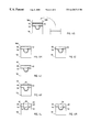
- FIG. 1 is a top view of a sensing element for a rotational accelerometer MEMS device
- FIGS. 2 (A) through 2 (D) are cross-sectional views of the structure illustrated in FIG. 1 along section lines A-A′, B-B′, C-C′ and D-D′, respectively;
- FIG. 3 is a partial top view of the structure illustrated in FIG. 1, particularly highlighting the cantilevers;
- FIGS. 4 (A) through 4 (M) illustrate the primary steps and stages of the preferred process for fabrication of a MEMS structure having opposing, interposed and interspaced projections according to the present invention.
- a rotary accelerometer sensor 40 comprises a generally circular, semiconductor mass 10 suspended relative to an annular support layer 54 by four equally spaced radially extending, flexible suspension projections 18 .
- the projections extend into the body 10 , are of relatively thin section, terminate in large-area tabs 19 and provide both rotary compliance and translational stiffness. Projections 18 form the suspension system for body 10 and do not, for all practical purposes, affect the capacitance as hereinafter explained.
- body 10 is formed to define a group of equally spaced and essentially constant width capacitive projections 20 which are integral with body 10 but extend radially outwardly therefrom. Projections 20 have rounded tips 24 which lengthen the sensor gap as hereinafter explained. The projections 20 effectively form one of two opposed capacitor plates as hereinafter explained.
- the suspension projections 18 do not form capacitor elements.
- the FIG. 1 structure further comprises a four-piece rim structure collectively defining the second capacitor plate.
- the rim structure comprises four identical quadrants each including a rim element 16 having opposite end areas adjacent but spaced from a tab 19 and tapering, triangular, inwardly-projecting capacitive projections 30 having wide base areas 32 and rounded tips 34 .
- Each projection 20 has one side lying adjacent and in closely and uniformly spaced relationship to a complemental side of a projection 30 to form a primary capacitive gap.
- the rim structure is etched such that the capacitive gap continues around the tips 24 and 34 to define an S-shape.
- the other sides of the projections 20 and 30 are more widely spaced from each other; i.e., two or three times the spacing of the primary gap, to greatly reduce the capacitive coupling therebetween.
- the circular body 10 is widely spaced from rim 16 so as to reduce capacitive coupling in the radial direction except at the tips of the projections.
- the suspension projections or tethers 18 flex to permit angular movement of the proof mass and the outwardly extending fingers 20 relative to the rim structure of the inwardly extending fingers 30 . This produces capacitive changes due to spacing variations in the primary gaps.
- the suspension elements 18 function essentially solely in a mechanical support, flexure suspension role and do not materially contribute to output signal quality.
- FIGS. 1 and 2 incorporates two structural design advantages for a MEMS device having opposing interposed and interspaced projections which will circumvent the adverse effects associated with the etch lag phenomenon.
- the projections 20 are relatively uniform in width along their lengths and have a high length to width ratio.
- the projections 30 are pyramidic in shape such that their sides are not parallel. As a result, however, one side of the first projection 20 and one side of the second projection 30 of each projection pair is substantially uniformly spaced apart from each other, along the length of the first projection 20 , by a distance substantially equal to the minimum capacitive gap.
- Projections 20 and 30 can, of course, have various shapes, e.g., straight, angled and curved, so long as the sensor gaps between them are of uniform width.
- projections 20 and 30 are prepared by the method of the invention which-avoids the over-etching associated with the etch lag phenomenon along wide trenches.
- electrical characteristics such as resistance and capacitance levels
- the electrical characteristics inherent in the thicker and wider structure of each projection.(finger) are at desired levels and are no longer adversely affected due to excess thinning of each projection due to the over-etching associated with the etch lag phenomenon.
- the tips 24 of the projections 20 are proximate to the rim 16 .
- the tips 24 are spaced from the rim 16 by a distance substantially equal to the capacitive gaps 36 .
- the rim 16 ! is preferably shaped such that the circumference of each tip 24 of each first projection 20 is substantially uniformly spaced from the rim 16 by a distance substantially equal to the primary capacitive gap.
- Such relatively close spacing between the tips 24 and the rim 16 is made possible by the method of the invention which avoids the over-etching associated with the etch lag phenomenon. The method of the invention avoids the tendency of prior art methods to excessively etch away tips 24 .
- the tips 34 of the projections 30 are proximate to the body mass 10 to circumvent the effects associated with etch lag.
- the tips 34 are spaced from the body mass 10 by a distance substantially equal to the capacitive gaps 36 .
- Such a close spacing between the tips, 34 and the body mass 10 ensures that over-etching associated with the etch lag; phenomenon will neither excessively etch away the tips 34 nor excessively etch into the body mass 10 .
- the body mass 10 is preferably shaped such that the circumference of each tip 34 of each second projection 30 is substantially uniformly spaced from the body mass 10 by a distance substantially equal to the primary capacitive gap.
- the natural structural consequence of the closer spacings between the tips 24 and the rim 16 is that at least one side of each of the bases 32 associated with the projections 30 is proximately located near one of the tips 24 by a distance substantially equal to the capacitive gap 36 .
- Such a closer spacing ensures that over-etching associated with the etch lag phenomenon will neither excessively etch into each of the bases 32 nor excessively etch away the tips 24 .
- the natural structural consequence of the closer spacings between the tips 34 and the body mass 10 is that at least one side of each of the bases 22 associated with the projections 20 is proximately located near one of the tips 34 by a distance substantially equal to the capacitive gap 36 .
- Such a closer spacing ensures that over-etching associated with the etch lag phenomenon will neither excessively etch into each of the bases 22 nor excessively etch away the tips 34 .
- the bases 22 of the projections 20 and the bases 32 of the projections 30 no longer have the tendency to be extraordinarily thin and fragile due to the etch lag phenomenon.
- the preferred structure according to the present invention helps eliminate the possibility that the projections 20 and the projections 30 may break off.
- FIGS. 2 (A) through 2 (D) are cross-sectional views of the structure illustrated in FIG. 1 positioned over a cavity 52 in a substrate 50 .
- An isolation layer 54 covers the substrate 50 as well as the lining of the cavity 52 .
- the semiconductor leer 14 is mounted on the isolation layer 54 at the periphery of the cavity 52 such that the body mass 10 is suspended above the cavity 52 via cantilever suspension projections 18 .
- Capacitive gaps 36 between the tips 24 of the first projections 20 and the rim 16 , and capacitive gaps 36 between the tips 34 of the second projections and the body 10 are particularly highlighted in FIGS. 2 (A) and 2 (B).
- the cantilevers 18 are attached to the body mass 10 at points 76 .
- the first projections 20 and the second projections 30 are defined in the semiconductor layer 14 .
- FIG. 3 is a partial top view of the structure illustrated in FIG. 1, particularly highlighting the cantilever 18 .
- the sense structure 40 has at least one cantilever 18 connected between the body 10 and the rim 16 .
- Each cantilever 18 thereby flexibly mounts the body 10 to the rim 16 such that the body 10 along with the rigid projections 20 are capable of rotational movement relative to the fixed surrounding structure including the projections 30 extending from the rim 16 .
- the ideal gap surrounding the suspension projections 18 is greater than the minimum (sensor) gap between projections 20 , 30 and equal to or smaller than the parasitic gap.
- Each cantilever 18 , the semiconductor layer 14 , the body 10 , the first projections 20 , and the second projections 30 are comprised of an electrically conductive, doped semiconductor material such that the differential capacitance between the first projections 20 and the second projections 30 can be electrically measured whenever the MEMS sense structure 40 experiences rotational acceleration caused by an external stimulus.
- the structure of a MEMS device may generally be fabricated by a bond/etch back technique.
- a first semiconductor substrate is formed and a cavity is thereafter etched into this first substrate.
- an oxidation step is carried out to thereby form an oxide layer (that is, an,isolation layer) over the surface and cavity of the first substrate.
- a second semiconductor substrate is formed separately from the first substrate.
- the top portion of this second substrate is typically very highly doped (that is, is highly concentrated) with p-type impurities, such as boron and/or germanium, to thereby create an etch termination layer (also sometimes referred to as an etch stop layer or a barrier layer).
- etching with an ICP DRIE (inductively coupled plasma deep reactive ion etch) machine through such a termination layer comprised of highly p-doped silicon, for example, is greatly attenuated.
- a lightly doped epitaxial semiconductor layer (sometimes referred to as an “epi-layer”) is grown on top of the second substrate. This epitaxial layer is to be the layer from which the structure of the MEMS device is ultimately defined and released.
- the second substrate along with its epitaxial layer is then inverted and bonded over the cavity in the first substrate such that the epitaxial layer covers the cavity and is bonded to the oxide layer (that is, isolation layer) at the periphery of the cavity.
- the oxide layer that is, isolation layer
- the epitaxial layer is thus situated directly above the cavity, and the highly p-doped portion (that is, the etch termination layer portion) of the second substrate is on top of the epitaxial layer.
- an etch process step is then typically attempted to precisely etch deep trenches through both the highly p-doped portion (the etch termination layer portion) of the second substrate and the epitaxial layer until the cavity underneath these layers is breached.
- the remaining portions of the etch termination layer portion of the second substrate and the remaining portions of the :epitaxial layer are together released and suspended above the cavity. These remaining unetched portions will then serve as the micro-machined structure of a MEMS device.
- a significant problem with the particular bond/etch back technique described above is that attempting to etch through both the highly p-doped portion (that is, the etch termination layer) of the second substrate and the lightly doped epitaxial layer simultaneously, during the same etching process step, often produces very poor and uneven sidewall profiles in the trenches being etched through these two layers. This is especially the case for the sidewalls of the trenches etched into the epitaxial layer.
- the sidewall profiles of the trenches etched into the epitaxial layer are typically not anisotropic in form.
- the sidewalls of the trenches are not substantially vertical and smooth, but are instead heavily striated or somewhat isotropic in form with undesired lateral etching into the. sidewalls of the trenches.
- the silicon (for example) of the epitaxial layer may be undesirably micro-masked as a result of the etch termination layer being incompletely etched, thereby undesirably causing silicon “spires” or “grass” to be formed on the sidewalls and bottoms within the epitaxial layer trenches.
- Such uneven etching through the epitaxial layer is most likely attributable to the disparity in the etch rates inherent in the highly p-doped portion (that is, the etch termination layer portion) of the second substrate and the lightly doped epitaxial layer.
- lateral etching into the sidewalls of: the trenches formed in the epitaxial layer ultimately produces a MEMS device structure which is malformed and rendered unfit for customer use.
- any silicon “spires” or “grass” undesirably formed within the trenches of the epitaxial layer often become particulates when the cavity underneath the epitaxial layer is breached during etching.
- FIGS. 4 (A) through 4 (M) illustrate the primary steps and stages of the preferred method/process for fabrication of the preferred MEMS structure according to the present invention.
- a first substrate 50 made from semiconductor material(s) is initially formed and provided.
- the first substrate 50 is made primarily of silicon.
- the first substrate 50 can instead be comprised with other materials as well, such as, for example, glass, ceramic, sapphire, and stainless steel.
- the first substrate 50 can be doped (or not doped at all) with either n-type or p-type impurities at any doping concentration level. This first substrate can be formed by any acceptable method known in the art.
- a cavity 52 is then etched into the first substrate 50 .
- the cavity 52 can be formed by any known conventional means, such as by a wet (chemical) etching technique or by a dry etching technique.
- an isolation layer 54 preferably comprised of silicon dioxide (commonly referred to as an “oxide layer”), is formed on the top surface of the first substrate 50 and the cavity 52 .
- Any conventional means known in the art can be used to grow the isolation layer 54 .
- One approach is to heat the first substrate 50 to a high temperature, for example, 850 to 1200 EC, in a controlled atmosphere containing either pure oxygen or water vapor. At such high temperatures, the oxygen and/or water vapor diffuse into and react with the silicon of the first substrate 50 , thereby forming the silicon dioxide layer 54 on the exposed top surface of the first substrate 50 .
- This silicon dioxide layer 54 serves as a bonding oxide, as a high-quality electrical insulator, and also as an etch termination layer.
- a second substrate 58 is formed and provided from semiconductor material(s), separately from the first substrate 50 .
- this second substrate 58 is made primarily of silicon.
- This second substrate 58 can be formed by any acceptable method known in the art.
- the top portion 58 A of the second substrate 58 is then doped with a high concentration of either n-type or p-type impurities to thereby transform the top portion 58 A of the second substrate 58 into an etch termination layer.
- the lower portion 58 B (that is, the non-termination layer portion) of the second substrate 58 is preferably left undoped. However, it is to be understood that the lower portion 58 B may alternatively be doped. In such a case, the lower portion 58 B must have a lower doping concentration than the top portion 58 A to ensure that the top portion 58 A can function as an etch termination layer.
- the top portion 58 A of the second substrate 58 is preferably doped with p-type impurities, including boron and germanium. These two p-type impurities can be introduced into the top portion 58 A of the second substrate 58 via a diffusion technique, via ion implantation, or, preferably, via in-situ doping during epitaxial silicon growth.
- a single-crystal epitaxial layer 60 preferably comprising silicon and lightly doped with a low concentration of either an n-type impurity or a p-type impurity, is grown on the etch termination layer portion 58 A of the second substrate 58 .
- this epitaxial layer 60 is lightly doped with a p-type impurity.
- This epitaxial layer 60 is formed by conventional means, preferably by a chemical vapor deposition process used to deposit additional silicon on the etch termination layer portion 58 A of the second substrate 58 and growing (that is, forming) a single-crystal silicon epitaxial layer 60 from the vapor phase (commonly referred to as “vapor-phase epitaxy”) on the etch termination layer 58 A.
- This single-crystal silicon epitaxial layer 60 can be doped with n-type impurities (such as phosphorus or arsenic) or, preferably, p-type impurities (such as, for example, boron or germanium) during the growth process by adding the impurities to the gas used during deposition of the additional silicon.
- n-type impurities such as phosphorus or arsenic
- p-type impurities such as, for example, boron or germanium
- the second substrate 58 (with the etch termination layer 58 A) along with the epitaxial layer 60 is then inverted and fusion bonded over the cavity 52 in the first substrate 50 such that the epitaxial layer 60 covers the cavity 50 and is bonded to the isolation layer 54 (preferably comprised of silicon dioxide) at the periphery of the cavity 52 .
- the isolation layer 54 preferably comprised of silicon dioxide
- the non-termination layer portion 58 B of the second substrate and then the heavily p-doped etch termination layer 58 A of the second substrate 58 are both first stripped away and entirely removed, as illustrated in FIGS. 4 (H) and 4 (I) according to the present invention, before etching through the epitaxial layer 60 is performed.
- This entire removal of the etch termination layer 58 A before etching through the epitaxial layer 60 helps to thereafter facilitate clean, anisotropic etching through the epitaxial layer 60 so that the sidewalls of the trenches etched into the epitaxial layer 60 are substantially vertical without significant lateral etching into the sidewalls, without significant vertical sidewall striations, and without the formation of silicon “grass.” Furthermore, the fact that the epitaxial layer 60 is lightly doped, as compared to the highly doped etch termination layer 58 A, helps facilitate the clean and highly selective removal of the etch termination layer 58 A from the epitaxial layer 60 . As a result of such selective removal, the thickness of the remaining epitaxial layer 60 tends to be more uniform.
- Such uniformity in the thickness of the epitaxial layer 60 helps ensure that trenches which are etched into the epitaxial layer 60 will breach the cavity 52 underneath the epitaxial layer 60 within a more predictable period of time.
- uniformity in the thickness of the epitaxial layer 60 enables process engineers, for example, to monitor the anticipated time periods for etching entirely through the epitaxial layer 60 to thereby avoid problems of over-etching and/or under-etching the epitaxial layer 60 .
- a layer of light-sensitive photoresist 62 is applied over the epitaxial layer 60 as illustrated in FIG. 4 (J).
- a positive type of photoresist should preferably be utilized instead of a negative type of photoresist.
- Positive photoresist facilitates better process control in this small-geometry structure.
- Application and formation of the photoresist layer 62 can typically be carried out by any known conventional means. This includes, for example, initially applying photoresist, in liquid form, over the epitaxial layer 60 .
- the bottom of the first substrate 50 is situated on a vacuum chuck and then spun at a high rate of speed to produce a thin layer of photoresist over the epitaxial layer 60 .
- the photoresist is then dried (sometimes referred to as “soft baking” or “pre-baking”) to improve adhesion of the photoresist layer 62 to the epitaxial layer 60 .
- the photoresist layer 62 is thereafter patterned according to a desired, predetermined shape of the structure of a MEMS device being fabricated, as illustrated in FIG. 4 (K).
- Patterning a layer of positive photoresist by conventional means typically involves the steps of, first, aligning a photomask over the photoresist layer. The photomask is pre-patterned according to the desired, predetermined shape of the MEMS structure to be fabricated. Next, some areas of the photoresist layer are selectively exposed to high-intensity ultraviolet light which is shown through the pre-patterned photomask onto the photoresist layer.
- trenches 66 are then anisotropically etched into the bare sections 64 of the epitaxial layer 60 until the cavity 52 underneath the epitaxial layer 60 is breached, as illustrated in FIG. 4 (L).
- a micromachined MEMS structure 70 is defined in the epitaxial layer 60 substantially within a single plane and is released above the cavity 52 . (Cantilevers which support and suspend the MEMS structure 70 above the cavity 52 are not shown in FIG. 4 (L)).
- the isolation layer 54 (preferably comprised of silicon dioxide) which lines the floor of the cavity 52 serves as an etch termination layer to prevent etching into the first substrate 50 once the cavity 52 is breached.
- This same isolation layer 54 also serves to both physically and electrically isolate the first substrate 50 from the epitaxial layer 60 .
- the first substrate 50 plays no role in the electrical functionality of the MEMS structure. As a result, there is no real necessity for doping the first substrate 50 , and process time, process complexity, and overall cost: is thereby reduced.
- any anisotropic etching technique may generally be utilized to etch the trenches 66 into the epitaxial layer 60 .
- the following high-precision, anisotropic etching technique may be utilized.
- the high-precision, anisotropic etching of the epitaxial layer 60 may be accomplished in an ALCATEL Comptech 602E deep silicon etch system at cryogenic temperatures (that is, temperatures less than approximately 173EK) using sulfur hexafluoride (SF 6 ) and oxygen (O 2 ) as the etch gases.
- ALCATEL Comptech is located in Fremont, Calif. and also has facilities in Annecy, Franceiand in Seoul, Korea. Preferred parameter settings for such a system which are necessary to execute such a high-precision, anisotropic etch are:
- substrate coolant flow He, 15 sccm
- the process time for etching may be varied as is appropriate for the desired etch depth and width for a given trench, as well as local and global plasma loading and diffusion effects. Ranges and variations in the above settings enable one to take into account minor adjustments in the plasma density and substrate bias to allow for the differences in the open area on the masks.
- the particular etch process parameters set forth above have produced aspect ratios of greater than 40:1 at 2 micrometer trench sizes. Furthermore, the above parameters have also produced an etch rate of 2.66 micrometers per minute in the minimum capacitive gaps of the MEMS structure illustrated in FIG. 1 .
- the particular exemplary MEMS structure in FIG. 1 is a capacitive rotational accelerometer.
- the low oxygen flow enhances performance of the etch system because,: generally, the higher the flow of oxygen, the faster the patterned photoresist mask layer 62 erodes during the etch. Since an oxygen plasma is used specifically for stripping photoresist, the low oxygen flow in the present etch system enables the deep trenches 66 to be etched into the bare sections 64 of the epitaxial layer 60 before the remaining patterned photoresist is eroded away. In this way, the deep trenches 66 can be etched into the epitaxial layer 60 by solely utilizing the patterned photoresist as an etch mask instead of also utilizing an inorganic hard mask.
- the epitaxial layer 60 is bathed with a halogen-containing plasma and a carbon compound-forming gas by any conventional means known in the art.
- Room temperature suitable for these processes is in a range of 273 EK ⁇ 25 EK.
- the oxygen in this preferred etch system functions as a passivation gas on the sidewalls of the trenches 66 .
- the oxygen reacts with the exposed silicon sidewalls to form silicon dioxide.
- the resulting thin oxide layer on the sidewalls of the trenches suffices as a passivation layer for the sidewall so that the etch through the epitaxial layer 610 remains anisotropic in nature.
- the oxygen flow is so low, the silicon etch rate is enhanced, leading to high aspect ratios of over 40: 1. Since the oxidation reaction of exposed silicon on the bottom of the deepening trench competes with the chemical and physical components of the silicon reaction with the etchant gas, a lower flow of oxygen favors the etch reaction, resulting in an enhanced etch rate.
- a properly micromachined MEMS structure that is released over the cavity 52 does not exhibit etch-related “stiction.” Stiction is a condition where smooth surfaces tend to adhere.
- stiction will render such a micromachined MEMS structure useless.
- this preferred etch method is stiction-free is a significant processing benefit.
- Photoresist removal can be accomplished by any known conventional means, such as, for example,i by utilizing conventional liquid resist strippers which cause the remaining photoresist to swell and lose adhesion to an underlying layer, in this case, the epitaxial layer 60 .
- Dry processing (sometimes referred to as “resist ashing”) or plasma ashing (a chemical reaction of O-radicals with carbon) is preferably used to remove the photoresist by oxidizing (that is, ashing) the photoresist in an oxygen plasma system.
- the electrically active elements and/or features (such as the body 10 , the projections 20 , the projections 30 , and the cantilevers 18 of FIG. 1) of the MEMS structure 70 , fabricated according to the present invention, are substantially contained within a single plane corresponding to the single-crystal, epitaxial layer 60 .
- the advantages of such are numerous, as set forth hereinbelow.
- the MEMS structure 70 can have a thicker roof height (the portion of the microshell that stands out over the active features/elements must generally be recessed into the top cap to assure no physical hindrance of rotational translation of the active features/elements). That is, in general, the thicker the roof of the top cap, the less sensitive the MEMS structure 70 is to breakage during packaging (for example, overmolding).
- utilizing a single-crystal epitaxial layer 60 is advantageous in that the inherent stress in a polysilicon film, is much harder to control than in a single-crystal epitaxial layer.
- undesired stress which is somewhat common in thick polysilicon films, can cause elastic deformation of the surface of the active elements/features or, in the worst case, can cause delamination of the film, thereby leading to imprecise gap sizes after etching.
- utilizing a substantially single-plane, single-crystal epitaxial layer avoids many of the problems typically associated with thermal expansion (such as undesirable changes in gap sizes and undesirable changes in capacitances between features separated by such gaps), and enables the simultaneous etching and delineation of both the active features/elements (including the body 10 , the projections 20 , the projections 30 , and the cantilevers 18 of FIG. 1) as well as any trenches which serve to electrically isolate active features/elements, metal lines/runners, and pads, as necessary, for proper electrical communication between the MEMS structure and any complementary circuitry or electronics.
- Such lateral release etches as are utilized in these other methods can include, but are not limited to, through-the-wafer etches; selective wet etches of an underlying layer (often an insulator, such as a buried oxide layer, which is common in SOI and SOS methods); a dry etch of an underlying layer (such as, for examples, a vapor phase hydrofluoric acid etch of a buried oxide, or a selective lateral etch of a buried layer in silicon, where the etchant species attacks a sub-surface layer selectively thereby freeing the MEMS structure from the substrate); and a set of methods where, after the vertical etch is complete, a non-selective lateral etch is performed at the bottom of the vertical etch thereby freeing the MEMS structure.
- selective wet etches of an underlying layer often an insulator, such as a buried oxide layer, which is common in SOI and SOS methods
- a dry etch of an underlying layer such as
- the lateral distances to be etched must necessarily be small. Such generally dictates that any large areas that need to be released, such as body masses, must be perforated at regular intervals to allow the lateral etch to free the area (for example, body mass) in an acceptable amount of time.
- the bond/etch-back method does not require such perforations.
- utilizing the bond/etch-back method, as uniquely implemented hereinabove is,the preferred method for fabricating MEMS structures, for it offers process advantages and saves cost.
- the lack of utilizing perforations in the bond/etch-back method allows for uni-body construction of the body mass, allows for a larger overall body mass, and thus allows for a larger rotational inertia for a same-sized body mass.
Abstract
Description
Claims (10)
Priority Applications (2)
| Application Number | Priority Date | Filing Date | Title |
|---|---|---|---|
| US09/410,713 US6428713B1 (en) | 1999-10-01 | 1999-10-01 | MEMS sensor structure and microfabrication process therefor |
| US10/141,740 US20020125208A1 (en) | 1999-10-01 | 2002-05-09 | MEMS sensor structure and microfabrication process therefor |
Applications Claiming Priority (1)
| Application Number | Priority Date | Filing Date | Title |
|---|---|---|---|
| US09/410,713 US6428713B1 (en) | 1999-10-01 | 1999-10-01 | MEMS sensor structure and microfabrication process therefor |
Related Child Applications (1)
| Application Number | Title | Priority Date | Filing Date |
|---|---|---|---|
| US10/141,740 Division US20020125208A1 (en) | 1999-10-01 | 2002-05-09 | MEMS sensor structure and microfabrication process therefor |
Publications (1)
| Publication Number | Publication Date |
|---|---|
| US6428713B1 true US6428713B1 (en) | 2002-08-06 |
Family
ID=23625922
Family Applications (2)
| Application Number | Title | Priority Date | Filing Date |
|---|---|---|---|
| US09/410,713 Expired - Lifetime US6428713B1 (en) | 1999-10-01 | 1999-10-01 | MEMS sensor structure and microfabrication process therefor |
| US10/141,740 Abandoned US20020125208A1 (en) | 1999-10-01 | 2002-05-09 | MEMS sensor structure and microfabrication process therefor |
Family Applications After (1)
| Application Number | Title | Priority Date | Filing Date |
|---|---|---|---|
| US10/141,740 Abandoned US20020125208A1 (en) | 1999-10-01 | 2002-05-09 | MEMS sensor structure and microfabrication process therefor |
Country Status (1)
| Country | Link |
|---|---|
| US (2) | US6428713B1 (en) |
Cited By (53)
| Publication number | Priority date | Publication date | Assignee | Title |
|---|---|---|---|---|
| US20020158040A1 (en) * | 2001-04-26 | 2002-10-31 | Lucak Mark A. | Method for fabricating a microelectromechanical system (MEMS) device using a pre-patterned substrate |
| US20020158039A1 (en) * | 2001-04-26 | 2002-10-31 | Harris Richard D. | Method for fabricating an isolated microelectromechanical system (MEMS) device using an internal void |
| US6487864B1 (en) * | 2002-04-23 | 2002-12-03 | Honeywell International Inc. | Cyrogenic inertial micro-electro-mechanical system (MEMS) device |
| US20030047308A1 (en) * | 2000-03-02 | 2003-03-13 | Hirsch John Michele | Wireless downwhole measurement and control for optimizing gas lift well and field performance |
| US20030060051A1 (en) * | 2001-09-26 | 2003-03-27 | Kretschmann Robert J. | Method for constructing an isolate microelectromechanical system (MEMS) device using surface fabrication techniques |
| US20030140700A1 (en) * | 2002-01-31 | 2003-07-31 | Zarabadi Seyed R. | Microfabricated linear accelerometer |
| US20030209768A1 (en) * | 2002-04-23 | 2003-11-13 | Milligan Donald J. | Micro-electromechanical actuator and methods of use and fabrication |
| US6675600B1 (en) | 2002-12-05 | 2004-01-13 | Bae Systems Information And Electronic Systems Integration Inc. | Thermal mismatch compensation technique for integrated circuit assemblies |
| US20040021403A1 (en) * | 2002-08-01 | 2004-02-05 | Georgia Tech Research Corporation | Piezoelectric on semiconductor-on-insulator microelectromechanical resonators and methods of fabrication |
| US6690178B2 (en) | 2001-10-26 | 2004-02-10 | Rockwell Automation Technologies, Inc. | On-board microelectromechanical system (MEMS) sensing device for power semiconductors |
| US6696364B2 (en) * | 2001-10-19 | 2004-02-24 | Stmicroelectronics S.R.L. | Method for manipulating MEMS devices, integrated on a wafer semiconductor and intended to be diced one from the other, and relevant support |
| US20040065940A1 (en) * | 2002-08-07 | 2004-04-08 | Farrokh Ayazi | Capacitive resonators and methods of fabrication |
| US6718826B2 (en) * | 2002-02-28 | 2004-04-13 | Delphi Technologies, Inc. | Balanced angular accelerometer |
| US20040074285A1 (en) * | 2002-10-17 | 2004-04-22 | Dimeo Frank | Apparatus and process for sensing fluoro species in semiconductor processing systems |
| US20040132227A1 (en) * | 2003-01-06 | 2004-07-08 | Horning Robert D. | Methods and structure for improving wafer bow control |
| US20040163444A1 (en) * | 2002-10-17 | 2004-08-26 | Dimeo Frank | Nickel-coated free-standing silicon carbide structure for sensing fluoro or halogen species in semiconductor processing systems, and processes of making and using same |
| US20040173575A1 (en) * | 2003-03-05 | 2004-09-09 | Ajay Kumar | Method of releasing devices from a substrate |
| US20040180464A1 (en) * | 2003-03-10 | 2004-09-16 | Horning Robert D. | Methods and systems for buried electrical feedthroughs in a glass-silicon mems process |
| US6798312B1 (en) | 1999-09-21 | 2004-09-28 | Rockwell Automation Technologies, Inc. | Microelectromechanical system (MEMS) analog electrical isolator |
| US20040187557A1 (en) * | 2002-10-17 | 2004-09-30 | Chen Philip S.H. | Apparatus and process for sensing target gas species in semiconductor processing systems |
| US20040187555A1 (en) * | 2003-03-27 | 2004-09-30 | Zarabadi Seyed R. | Self-test circuit and method for testing a microsensor |
| US20040189142A1 (en) * | 2003-03-25 | 2004-09-30 | Knieser Michael J. | Microelectromechanical isolating circuit |
| US20040246306A1 (en) * | 2000-02-03 | 2004-12-09 | Scott Adams | Electrostatic actuator for microelectromechanical systems and methods of fabrication |
| US6879016B1 (en) * | 2002-10-07 | 2005-04-12 | Zyvex Corporation | Microcomponent having intra-layer electrical isolation with mechanical robustness |
| US20050121735A1 (en) * | 2001-08-24 | 2005-06-09 | Honeywell International, Inc. | Hermetically sealed silicon micro-machined electromechanical system (MEMS) device having diffused conductors |
| US20050139967A1 (en) * | 2003-12-24 | 2005-06-30 | Honeywell International, Inc. | Signal routing in a hermetically sealed MEMS device |
| US20050235751A1 (en) * | 2004-04-27 | 2005-10-27 | Zarabadi Seyed R | Dual-axis accelerometer |
| US20050239231A1 (en) * | 2004-04-27 | 2005-10-27 | Przybyla James R | Method for making a microelectromechanical system using a flexure protection layer |
| US20050240374A1 (en) * | 2004-04-27 | 2005-10-27 | Zarabadi Seyed R | Circuit and method of processing multiple-axis sensor output signals |
| US6991957B2 (en) | 2001-08-20 | 2006-01-31 | Honeywell International, Inc. | Micro-machined electromechanical system (MEMS) accelerometer device having arcuately shaped flexures |
| US20060051883A1 (en) * | 2004-07-13 | 2006-03-09 | Mescher Mark J | Apparatus and system for suspending a chip-scale device and related methods |
| EP1659383A2 (en) | 2004-11-23 | 2006-05-24 | Delphi Technologies, Inc. | Capacitive strain gauge |
| EP1690192A2 (en) * | 2003-11-04 | 2006-08-16 | Lockheed Martin Corporation | Locomotive location system and method |
| EP1703287A1 (en) | 2005-03-16 | 2006-09-20 | Delphi Technologies, Inc. | Multiple-axis linear accelerometer |
| US20060211161A1 (en) * | 2005-03-16 | 2006-09-21 | Christenson John C | Method of making microsensor |
| US7140250B2 (en) | 2005-02-18 | 2006-11-28 | Honeywell International Inc. | MEMS teeter-totter accelerometer having reduced non-linearty |
| US7224035B1 (en) | 2002-10-07 | 2007-05-29 | Zyvex Corporation | Apparatus and fabrication methods for incorporating sub-millimeter, high-resistivity mechanical components with low-resistivity conductors while maintaining electrical isolation therebetween |
| US20070237959A1 (en) * | 2005-09-06 | 2007-10-11 | Lemaire Charles A | Apparatus and method for growing fullerene nanotube forests, and forming nanotube films, threads and composite structures therefrom |
| US20070251592A1 (en) * | 2006-05-01 | 2007-11-01 | Christenson John C | Microfluidic valve structure |
| US20070298613A1 (en) * | 2006-06-21 | 2007-12-27 | Yu-Fu Kang | Method of manufacturing suspension structure |
| US20080018012A1 (en) * | 2005-09-06 | 2008-01-24 | Lemaire Alexander B | Apparatus and method for growing fullerene nanotube forests, and forming nanotube films, threads and composite structures therefrom |
| US20080134757A1 (en) * | 2005-03-16 | 2008-06-12 | Advanced Technology Materials, Inc. | Method And Apparatus For Monitoring Plasma Conditions In An Etching Plasma Processing Facility |
| US20090031809A1 (en) * | 2007-08-03 | 2009-02-05 | Freescale Semiconductor, Inc. | Symmetrical differential capacitive sensor and method of making same |
| US7494593B1 (en) | 2004-06-28 | 2009-02-24 | Hewlett-Packard Development Company, L.P. | Method for forming a cantilever and tip |
| US20100122578A1 (en) * | 2008-11-17 | 2010-05-20 | Johannes Classen | Micromechanical component |
| US20100176466A1 (en) * | 2009-01-09 | 2010-07-15 | Denso Corporation | Semiconductor device and method of making the same |
| US20100308444A1 (en) * | 2009-06-04 | 2010-12-09 | Taiwan Semiconductor Manufacturing Company, Ltd. | Method of Manufacturing an Electronic Device |
| US20110049648A1 (en) * | 2009-08-26 | 2011-03-03 | Freescale Semiconductor, Inc. | Mems device with stress isolation and method of fabrication |
| US20120247645A1 (en) * | 2009-11-30 | 2012-10-04 | Mitsubishi Heavy Industiries, Ltd. | Bonding method, bonding apparatus, and bonding system |
| US8372677B2 (en) | 2006-05-10 | 2013-02-12 | Qualtre, Inc. | Three-axis accelerometers and fabrication methods |
| US9446938B2 (en) | 2013-05-09 | 2016-09-20 | Denso Corporation | SOI substrate, physical quantity sensor, SOI substrate manufacturing method, and physical quantity sensor manufacturing method |
| CN107867673A (en) * | 2016-09-27 | 2018-04-03 | 英飞凌科技股份有限公司 | The processing method of single crystalline substrate and micro mechanical structure |
| US9970764B2 (en) | 2009-08-31 | 2018-05-15 | Georgia Tech Research Corporation | Bulk acoustic wave gyroscope with spoked structure |
Families Citing this family (17)
| Publication number | Priority date | Publication date | Assignee | Title |
|---|---|---|---|---|
| US7335426B2 (en) * | 1999-11-19 | 2008-02-26 | Advanced Bio Prosthetic Surfaces, Ltd. | High strength vacuum deposited nitinol alloy films and method of making same |
| US6762116B1 (en) * | 2002-06-12 | 2004-07-13 | Zyvex Corporation | System and method for fabricating microcomponent parts on a substrate having pre-fabricated electronic circuitry thereon |
| US7096568B1 (en) | 2003-07-10 | 2006-08-29 | Zyvex Corporation | Method of manufacturing a microcomponent assembly |
| WO2005027785A2 (en) * | 2003-09-18 | 2005-03-31 | Advanced Bio Prosthetic Surfaces, Ltd. | Medical device having mems functionality and methods of making same |
| US20050132803A1 (en) * | 2003-12-23 | 2005-06-23 | Baldwin David J. | Low cost integrated MEMS hybrid |
| US7025619B2 (en) * | 2004-02-13 | 2006-04-11 | Zyvex Corporation | Sockets for microassembly |
| US6923669B1 (en) * | 2004-02-13 | 2005-08-02 | Zyvex Corporation | Microconnectors and non-powered microassembly therewith |
| US6956219B2 (en) * | 2004-03-12 | 2005-10-18 | Zyvex Corporation | MEMS based charged particle deflector design |
| US7081630B2 (en) * | 2004-03-12 | 2006-07-25 | Zyvex Corporation | Compact microcolumn for automated assembly |
| WO2005122217A1 (en) * | 2004-06-09 | 2005-12-22 | The Regents Of The University Of California | Thermosetting polymer bonding for micro electro-mechanical systems |
| US7314382B2 (en) | 2005-05-18 | 2008-01-01 | Zyvex Labs, Llc | Apparatus and methods of manufacturing and assembling microscale and nanoscale components and assemblies |
| JP4534041B2 (en) * | 2005-08-02 | 2010-09-01 | 株式会社デンソー | Manufacturing method of semiconductor device |
| US8008735B2 (en) | 2006-03-20 | 2011-08-30 | Semiconductor Energy Laboratory Co., Ltd. | Micromachine device with a spatial portion formed within |
| TWI305930B (en) * | 2006-06-19 | 2009-02-01 | Touch Micro System Tech | Method of fabricating suspended structure |
| US7605377B2 (en) | 2006-10-17 | 2009-10-20 | Zyvex Corporation | On-chip reflectron and ion optics |
| US20090001489A1 (en) * | 2007-06-26 | 2009-01-01 | Yue-Ming Hsin | Silicon photodetector and method for forming the same |
| US8984942B2 (en) | 2012-02-10 | 2015-03-24 | Hewlett-Packard Development Company, L.P. | Suspended masses in micro-mechanical devices |
Citations (4)
| Publication number | Priority date | Publication date | Assignee | Title |
|---|---|---|---|---|
| US5251484A (en) | 1992-04-03 | 1993-10-12 | Hewlett-Packard Company | Rotational accelerometer |
| US5447601A (en) * | 1993-04-07 | 1995-09-05 | British Aerospace Plc | Method of manufacturing a motion sensor |
| US5840199A (en) * | 1994-06-01 | 1998-11-24 | Litton Systems, Inc. | Method for purging a multi-layer sacrificial etched silicon substrate |
| US6174820B1 (en) * | 1999-02-16 | 2001-01-16 | Sandia Corporation | Use of silicon oxynitride as a sacrificial material for microelectromechanical devices |
-
1999
- 1999-10-01 US US09/410,713 patent/US6428713B1/en not_active Expired - Lifetime
-
2002
- 2002-05-09 US US10/141,740 patent/US20020125208A1/en not_active Abandoned
Patent Citations (4)
| Publication number | Priority date | Publication date | Assignee | Title |
|---|---|---|---|---|
| US5251484A (en) | 1992-04-03 | 1993-10-12 | Hewlett-Packard Company | Rotational accelerometer |
| US5447601A (en) * | 1993-04-07 | 1995-09-05 | British Aerospace Plc | Method of manufacturing a motion sensor |
| US5840199A (en) * | 1994-06-01 | 1998-11-24 | Litton Systems, Inc. | Method for purging a multi-layer sacrificial etched silicon substrate |
| US6174820B1 (en) * | 1999-02-16 | 2001-01-16 | Sandia Corporation | Use of silicon oxynitride as a sacrificial material for microelectromechanical devices |
Non-Patent Citations (3)
| Title |
|---|
| "Embedded Interconnect and Electrical Isolation for High-Aspect-Ratio, SOI Inertial Instruments" T. J. Brosnihan, J.F. Bustillo, A.P. Pisano and R.T. Howe, 1996 International Conference on Solid-State Sensors and Actuators, Chicago, Jun. 16-19, 1997, pp. 637-640. |
| "Increased Disturbance Rejection in Magnetic Disk Drives by Acceleration Feedforward Control and Parameter Adaption" M.T. White and M. Tomizuka, vol. 5, No. 6, 1997, pp. 741-751. |
| "Rejecting Rotational Disturbances on Small Disk Drives Using Rotational Accelerometers" Daniel Y. Abramovitch, 1996 IFAC World Congress in San Francisco, CA 1996, pp. 1-6. |
Cited By (111)
| Publication number | Priority date | Publication date | Assignee | Title |
|---|---|---|---|---|
| US6798312B1 (en) | 1999-09-21 | 2004-09-28 | Rockwell Automation Technologies, Inc. | Microelectromechanical system (MEMS) analog electrical isolator |
| US20040246306A1 (en) * | 2000-02-03 | 2004-12-09 | Scott Adams | Electrostatic actuator for microelectromechanical systems and methods of fabrication |
| US7261826B2 (en) * | 2000-02-03 | 2007-08-28 | Calient Networks, Inc. | Electrostatic actuator for microelectromechanical systems and methods of fabrication |
| US20030047308A1 (en) * | 2000-03-02 | 2003-03-13 | Hirsch John Michele | Wireless downwhole measurement and control for optimizing gas lift well and field performance |
| US7387737B2 (en) * | 2001-04-26 | 2008-06-17 | Rockwell Automation Technologies, Inc. | Method for fabricating an isolated microelectromechanical system (MEMS) device using an internal void |
| US6761829B2 (en) * | 2001-04-26 | 2004-07-13 | Rockwell Automation Technologies, Inc. | Method for fabricating an isolated microelectromechanical system (MEMS) device using an internal void |
| US20020158040A1 (en) * | 2001-04-26 | 2002-10-31 | Lucak Mark A. | Method for fabricating a microelectromechanical system (MEMS) device using a pre-patterned substrate |
| US20060096947A1 (en) * | 2001-04-26 | 2006-05-11 | Harris Richard D | Method for fabricating an isolated microelectromechanical system (MEMS) device using an internal void |
| US6815243B2 (en) | 2001-04-26 | 2004-11-09 | Rockwell Automation Technologies, Inc. | Method of fabricating a microelectromechanical system (MEMS) device using a pre-patterned substrate |
| US20020158039A1 (en) * | 2001-04-26 | 2002-10-31 | Harris Richard D. | Method for fabricating an isolated microelectromechanical system (MEMS) device using an internal void |
| US6991957B2 (en) | 2001-08-20 | 2006-01-31 | Honeywell International, Inc. | Micro-machined electromechanical system (MEMS) accelerometer device having arcuately shaped flexures |
| US6906395B2 (en) | 2001-08-24 | 2005-06-14 | Honeywell International, Inc. | Hermetically sealed silicon micro-machined electromechanical system (MEMS) device having diffused conductors |
| US20050121735A1 (en) * | 2001-08-24 | 2005-06-09 | Honeywell International, Inc. | Hermetically sealed silicon micro-machined electromechanical system (MEMS) device having diffused conductors |
| US20030060051A1 (en) * | 2001-09-26 | 2003-03-27 | Kretschmann Robert J. | Method for constructing an isolate microelectromechanical system (MEMS) device using surface fabrication techniques |
| US6756310B2 (en) | 2001-09-26 | 2004-06-29 | Rockwell Automation Technologies, Inc. | Method for constructing an isolate microelectromechanical system (MEMS) device using surface fabrication techniques |
| US6696364B2 (en) * | 2001-10-19 | 2004-02-24 | Stmicroelectronics S.R.L. | Method for manipulating MEMS devices, integrated on a wafer semiconductor and intended to be diced one from the other, and relevant support |
| US6690178B2 (en) | 2001-10-26 | 2004-02-10 | Rockwell Automation Technologies, Inc. | On-board microelectromechanical system (MEMS) sensing device for power semiconductors |
| US6761070B2 (en) | 2002-01-31 | 2004-07-13 | Delphi Technologies, Inc. | Microfabricated linear accelerometer |
| US20030140700A1 (en) * | 2002-01-31 | 2003-07-31 | Zarabadi Seyed R. | Microfabricated linear accelerometer |
| US6718826B2 (en) * | 2002-02-28 | 2004-04-13 | Delphi Technologies, Inc. | Balanced angular accelerometer |
| US6897083B2 (en) * | 2002-04-23 | 2005-05-24 | Hewlett-Packard Development Company, L.P. | Micro-electromechanical actuator and methods of use and fabrication |
| US6487864B1 (en) * | 2002-04-23 | 2002-12-03 | Honeywell International Inc. | Cyrogenic inertial micro-electro-mechanical system (MEMS) device |
| US20030209768A1 (en) * | 2002-04-23 | 2003-11-13 | Milligan Donald J. | Micro-electromechanical actuator and methods of use and fabrication |
| US20040021403A1 (en) * | 2002-08-01 | 2004-02-05 | Georgia Tech Research Corporation | Piezoelectric on semiconductor-on-insulator microelectromechanical resonators and methods of fabrication |
| US6909221B2 (en) | 2002-08-01 | 2005-06-21 | Georgia Tech Research Corporation | Piezoelectric on semiconductor-on-insulator microelectromechanical resonators |
| US20060273416A1 (en) * | 2002-08-07 | 2006-12-07 | Farrokh Ayazi | Capacitive resonators |
| US7023065B2 (en) | 2002-08-07 | 2006-04-04 | Georgia Tech Research Corporation | Capacitive resonators and methods of fabrication |
| US20040065940A1 (en) * | 2002-08-07 | 2004-04-08 | Farrokh Ayazi | Capacitive resonators and methods of fabrication |
| US6879016B1 (en) * | 2002-10-07 | 2005-04-12 | Zyvex Corporation | Microcomponent having intra-layer electrical isolation with mechanical robustness |
| US7224035B1 (en) | 2002-10-07 | 2007-05-29 | Zyvex Corporation | Apparatus and fabrication methods for incorporating sub-millimeter, high-resistivity mechanical components with low-resistivity conductors while maintaining electrical isolation therebetween |
| CN1705871B (en) * | 2002-10-17 | 2011-06-15 | 高级技术材料公司 | Apparatus and process for sensing fluoro species in semiconductor processing systems |
| US20040163444A1 (en) * | 2002-10-17 | 2004-08-26 | Dimeo Frank | Nickel-coated free-standing silicon carbide structure for sensing fluoro or halogen species in semiconductor processing systems, and processes of making and using same |
| US8109130B2 (en) | 2002-10-17 | 2012-02-07 | Advanced Technology Materials, Inc. | Apparatus and process for sensing fluoro species in semiconductor processing systems |
| US7228724B2 (en) | 2002-10-17 | 2007-06-12 | Advanced Technology Materials, Inc. | Apparatus and process for sensing target gas species in semiconductor processing systems |
| US7296460B2 (en) | 2002-10-17 | 2007-11-20 | Advanced Technology Materials, Inc. | Apparatus and process for sensing fluoro species in semiconductor processing systems |
| WO2004036175A2 (en) * | 2002-10-17 | 2004-04-29 | Advanced Technology Materials, Inc. | Apparatus and process for sensing fluoro species in semiconductor processing systems |
| US20040074285A1 (en) * | 2002-10-17 | 2004-04-22 | Dimeo Frank | Apparatus and process for sensing fluoro species in semiconductor processing systems |
| US7475588B2 (en) | 2002-10-17 | 2009-01-13 | Advanced Technology Materials, Inc. | Apparatus and process for sensing fluoro species in semiconductor processing systems |
| WO2004036175A3 (en) * | 2002-10-17 | 2004-06-17 | Advanced Tech Materials | Apparatus and process for sensing fluoro species in semiconductor processing systems |
| US7296458B2 (en) | 2002-10-17 | 2007-11-20 | Advanced Technology Materials, Inc | Nickel-coated free-standing silicon carbide structure for sensing fluoro or halogen species in semiconductor processing systems, and processes of making and using same |
| US20090305427A1 (en) * | 2002-10-17 | 2009-12-10 | Advanced Technology Materials, Inc. | Apparatus and process for sensing fluoro species in semiconductor processing systems |
| US7080545B2 (en) | 2002-10-17 | 2006-07-25 | Advanced Technology Materials, Inc. | Apparatus and process for sensing fluoro species in semiconductor processing systems |
| US20050199496A1 (en) * | 2002-10-17 | 2005-09-15 | Dimeo Frank Jr. | Apparatus and process for sensing fluoro species in semiconductor processing systems |
| US20050205424A1 (en) * | 2002-10-17 | 2005-09-22 | Dimeo Frank Jr | Apparatus and process for sensing fluoro species in semiconductor processing systems |
| US20040187557A1 (en) * | 2002-10-17 | 2004-09-30 | Chen Philip S.H. | Apparatus and process for sensing target gas species in semiconductor processing systems |
| US6675600B1 (en) | 2002-12-05 | 2004-01-13 | Bae Systems Information And Electronic Systems Integration Inc. | Thermal mismatch compensation technique for integrated circuit assemblies |
| US20040132227A1 (en) * | 2003-01-06 | 2004-07-08 | Horning Robert D. | Methods and structure for improving wafer bow control |
| US6770504B2 (en) | 2003-01-06 | 2004-08-03 | Honeywell International Inc. | Methods and structure for improving wafer bow control |
| US20050050971A1 (en) * | 2003-01-06 | 2005-03-10 | Horning Robert D. | Methods and structure for improving wafer bow control |
| US20040173575A1 (en) * | 2003-03-05 | 2004-09-09 | Ajay Kumar | Method of releasing devices from a substrate |
| US6905616B2 (en) | 2003-03-05 | 2005-06-14 | Applied Materials, Inc. | Method of releasing devices from a substrate |
| US20040180464A1 (en) * | 2003-03-10 | 2004-09-16 | Horning Robert D. | Methods and systems for buried electrical feedthroughs in a glass-silicon mems process |
| US6924165B2 (en) | 2003-03-10 | 2005-08-02 | Honeywell International Inc. | Methods and systems for buried electrical feedthroughs in a glass-silicon MEMS process |
| US6888233B2 (en) | 2003-03-10 | 2005-05-03 | Honeywell International Inc. | Systems for buried electrical feedthroughs in a glass-silicon MEMS process |
| US20040244484A1 (en) * | 2003-03-10 | 2004-12-09 | Horning Robert D. | Methods and systems for buried electrical feedthroughs in a glass-silicon MEMS process |
| US20040189142A1 (en) * | 2003-03-25 | 2004-09-30 | Knieser Michael J. | Microelectromechanical isolating circuit |
| US6975193B2 (en) | 2003-03-25 | 2005-12-13 | Rockwell Automation Technologies, Inc. | Microelectromechanical isolating circuit |
| US20040187555A1 (en) * | 2003-03-27 | 2004-09-30 | Zarabadi Seyed R. | Self-test circuit and method for testing a microsensor |
| US6918282B2 (en) | 2003-03-27 | 2005-07-19 | Delphi Technologies, Inc. | Self-test circuit and method for testing a microsensor |
| EP1690192A2 (en) * | 2003-11-04 | 2006-08-16 | Lockheed Martin Corporation | Locomotive location system and method |
| EP1690192A4 (en) * | 2003-11-04 | 2009-03-11 | Lockheed Corp | Locomotive location system and method |
| US20050139967A1 (en) * | 2003-12-24 | 2005-06-30 | Honeywell International, Inc. | Signal routing in a hermetically sealed MEMS device |
| US6949807B2 (en) | 2003-12-24 | 2005-09-27 | Honeywell International, Inc. | Signal routing in a hermetically sealed MEMS device |
| US7194376B2 (en) | 2004-04-27 | 2007-03-20 | Delphi Technologies, Inc. | Circuit and method of processing multiple-axis sensor output signals |
| US20050240374A1 (en) * | 2004-04-27 | 2005-10-27 | Zarabadi Seyed R | Circuit and method of processing multiple-axis sensor output signals |
| US7056759B2 (en) | 2004-04-27 | 2006-06-06 | Hewlett-Packard Development Company, L.P. | Method for making a microelectromechanical system using a flexure protection layer |
| US20050239231A1 (en) * | 2004-04-27 | 2005-10-27 | Przybyla James R | Method for making a microelectromechanical system using a flexure protection layer |
| US20050235751A1 (en) * | 2004-04-27 | 2005-10-27 | Zarabadi Seyed R | Dual-axis accelerometer |
| US7494593B1 (en) | 2004-06-28 | 2009-02-24 | Hewlett-Packard Development Company, L.P. | Method for forming a cantilever and tip |
| US20060051883A1 (en) * | 2004-07-13 | 2006-03-09 | Mescher Mark J | Apparatus and system for suspending a chip-scale device and related methods |
| US7215213B2 (en) | 2004-07-13 | 2007-05-08 | Charles Stark Draper Laboratory, Inc., The | Apparatus and system for suspending a chip-scale device and related methods |
| EP1659383A2 (en) | 2004-11-23 | 2006-05-24 | Delphi Technologies, Inc. | Capacitive strain gauge |
| US20060107768A1 (en) * | 2004-11-23 | 2006-05-25 | Johnson Jack D | Capacitive strain gauge |
| US7204162B2 (en) | 2004-11-23 | 2007-04-17 | Delphi Technologies, Inc. | Capacitive strain gauge |
| US7140250B2 (en) | 2005-02-18 | 2006-11-28 | Honeywell International Inc. | MEMS teeter-totter accelerometer having reduced non-linearty |
| EP1703287A1 (en) | 2005-03-16 | 2006-09-20 | Delphi Technologies, Inc. | Multiple-axis linear accelerometer |
| EP1702884A3 (en) * | 2005-03-16 | 2011-01-05 | Delphi Technologies, Inc. | Method of making a microsensor |
| US7293460B2 (en) | 2005-03-16 | 2007-11-13 | Delphi Technologies, Inc. | Multiple-axis linear accelerometer |
| US20080134757A1 (en) * | 2005-03-16 | 2008-06-12 | Advanced Technology Materials, Inc. | Method And Apparatus For Monitoring Plasma Conditions In An Etching Plasma Processing Facility |
| US7250322B2 (en) * | 2005-03-16 | 2007-07-31 | Delphi Technologies, Inc. | Method of making microsensor |
| US20060211161A1 (en) * | 2005-03-16 | 2006-09-21 | Christenson John C | Method of making microsensor |
| US20060207327A1 (en) * | 2005-03-16 | 2006-09-21 | Zarabadi Seyed R | Linear accelerometer |
| US9815697B2 (en) | 2005-09-06 | 2017-11-14 | Grandnano, Llc | Apparatus for growing carbon nanotube forests, and generating nanotube structures therefrom, and method |
| US20080018012A1 (en) * | 2005-09-06 | 2008-01-24 | Lemaire Alexander B | Apparatus and method for growing fullerene nanotube forests, and forming nanotube films, threads and composite structures therefrom |
| US8162643B2 (en) | 2005-09-06 | 2012-04-24 | Lemaire Alexander B | Method and apparatus for growing nanotube forests, and generating nanotube structures therefrom |
| US8845941B2 (en) | 2005-09-06 | 2014-09-30 | Grandnano, Llc | Apparatus for growing carbon nanotube forests, and generating nanotube structures therefrom, and method |
| US20070237959A1 (en) * | 2005-09-06 | 2007-10-11 | Lemaire Charles A | Apparatus and method for growing fullerene nanotube forests, and forming nanotube films, threads and composite structures therefrom |
| US8551376B2 (en) | 2005-09-06 | 2013-10-08 | Grandnano, Llc | Method for growing carbon nanotube forests, and generating nanotube structures therefrom, and apparatus |
| US7744793B2 (en) | 2005-09-06 | 2010-06-29 | Lemaire Alexander B | Apparatus and method for growing fullerene nanotube forests, and forming nanotube films, threads and composite structures therefrom |
| US7850778B2 (en) | 2005-09-06 | 2010-12-14 | Lemaire Charles A | Apparatus and method for growing fullerene nanotube forests, and forming nanotube films, threads and composite structures therefrom |
| US20070251592A1 (en) * | 2006-05-01 | 2007-11-01 | Christenson John C | Microfluidic valve structure |
| US8256465B2 (en) | 2006-05-01 | 2012-09-04 | Google Inc. | Microfluidic valve structure |
| US8372677B2 (en) | 2006-05-10 | 2013-02-12 | Qualtre, Inc. | Three-axis accelerometers and fabrication methods |
| US20070298613A1 (en) * | 2006-06-21 | 2007-12-27 | Yu-Fu Kang | Method of manufacturing suspension structure |
| US7432208B2 (en) | 2006-06-21 | 2008-10-07 | Touch Micro-System Technology Inc. | Method of manufacturing suspension structure |
| WO2009020716A1 (en) * | 2007-08-03 | 2009-02-12 | Freescale Semiconductor Inc. | Symmetrical differential capacitive sensor and method of making same |
| US7578190B2 (en) | 2007-08-03 | 2009-08-25 | Freescale Semiconductor, Inc. | Symmetrical differential capacitive sensor and method of making same |
| US20090031809A1 (en) * | 2007-08-03 | 2009-02-05 | Freescale Semiconductor, Inc. | Symmetrical differential capacitive sensor and method of making same |
| US20100122578A1 (en) * | 2008-11-17 | 2010-05-20 | Johannes Classen | Micromechanical component |
| US8806940B2 (en) * | 2008-11-17 | 2014-08-19 | Robert Bosch Gmbh | Micromechanical component |
| US20100176466A1 (en) * | 2009-01-09 | 2010-07-15 | Denso Corporation | Semiconductor device and method of making the same |
| US8283738B2 (en) * | 2009-01-09 | 2012-10-09 | Denso Corporation | Semiconductor device including sensor member and cap member and method of making the same |
| US20100308444A1 (en) * | 2009-06-04 | 2010-12-09 | Taiwan Semiconductor Manufacturing Company, Ltd. | Method of Manufacturing an Electronic Device |
| US8564103B2 (en) * | 2009-06-04 | 2013-10-22 | Taiwan Semiconductor Manufacturing Company, Ltd. | Method of manufacturing an electronic device |
| US8810030B2 (en) | 2009-08-26 | 2014-08-19 | Freescale Semiconductor, Inc. | MEMS device with stress isolation and method of fabrication |
| US8138007B2 (en) | 2009-08-26 | 2012-03-20 | Freescale Semiconductor, Inc. | MEMS device with stress isolation and method of fabrication |
| US20110049648A1 (en) * | 2009-08-26 | 2011-03-03 | Freescale Semiconductor, Inc. | Mems device with stress isolation and method of fabrication |
| US9970764B2 (en) | 2009-08-31 | 2018-05-15 | Georgia Tech Research Corporation | Bulk acoustic wave gyroscope with spoked structure |
| US20120247645A1 (en) * | 2009-11-30 | 2012-10-04 | Mitsubishi Heavy Industiries, Ltd. | Bonding method, bonding apparatus, and bonding system |
| US9446938B2 (en) | 2013-05-09 | 2016-09-20 | Denso Corporation | SOI substrate, physical quantity sensor, SOI substrate manufacturing method, and physical quantity sensor manufacturing method |
| CN107867673A (en) * | 2016-09-27 | 2018-04-03 | 英飞凌科技股份有限公司 | The processing method of single crystalline substrate and micro mechanical structure |
Also Published As
| Publication number | Publication date |
|---|---|
| US20020125208A1 (en) | 2002-09-12 |
Similar Documents
| Publication | Publication Date | Title |
|---|---|---|
| US6428713B1 (en) | MEMS sensor structure and microfabrication process therefor | |
| US5840199A (en) | Method for purging a multi-layer sacrificial etched silicon substrate | |
| US5476819A (en) | Substrate anchor for undercut silicon on insulator microstructures | |
| US5883012A (en) | Method of etching a trench into a semiconductor substrate | |
| KR100692593B1 (en) | Manufacturing method of mems structure | |
| JP5602761B2 (en) | Micro-electromechanical system device having separated microstructure and manufacturing method thereof | |
| KR100348177B1 (en) | Isolation Method for Single Crystalline Silicon Micro Machining using Deep Trench Dielectric Layer | |
| US20040099631A1 (en) | Deep reactive ion etching process and microelectromechanical devices formed thereby | |
| JP3762928B2 (en) | Micromechanical sensor and manufacturing method thereof | |
| US7122395B2 (en) | Method of forming semiconductor devices through epitaxy | |
| US6569702B2 (en) | Triple layer isolation for silicon microstructure and structures formed using the same | |
| US6916728B2 (en) | Method for forming a semiconductor structure through epitaxial growth | |
| KR100373739B1 (en) | Method for Fabrication of Electrostatic Vertical Actuators Using One Single-crystalline Silicon Wafer | |
| JPH11261079A (en) | Semiconductor element and its manufacture | |
| EP1433199B1 (en) | Method for forming a cavity structure in an soi substrate and cavity structure formed in an soi substrate | |
| KR19980070286A (en) | Silicon micromachining apparatus and manufacturing method thereof | |
| KR100817813B1 (en) | A method for fabricating a micro structures with multi differential gap on silicon substrate | |
| US6790699B2 (en) | Method for manufacturing a semiconductor device | |
| JPH11274142A (en) | Etching depth detecting method, manufacture of semiconductor device using the method, and manufacture of dynamical quantity sensor using the detecting method | |
| JPH06302834A (en) | Manufacture of thin-film structure | |
| CN218841706U (en) | Self-aligned polycrystalline silicon and monocrystalline silicon hybrid MEMS vertical comb electrode | |
| JPH11186567A (en) | Manufacture of semiconductor mechanical quantity sensor | |
| KR101539197B1 (en) | Method of micromachining having improved movement performance along z-axis and minimized structure depth variance, and accelerometer using the same | |
| CN115784143A (en) | Self-aligned polycrystalline silicon and monocrystalline silicon hybrid MEMS vertical electrode and manufacturing method thereof | |
| WO1997022140A2 (en) | Method for purging a multi-layer sacrificial etched silicon substrate |
Legal Events
| Date | Code | Title | Description |
|---|---|---|---|
| AS | Assignment |
Owner name: DELPHI TECHNOLOGIES, INC., MICHIGAN Free format text: ASSIGNMENT OF ASSIGNORS INTEREST;ASSIGNORS:CHRISTENSON, JOHN CARL;STALLER, STEVEN EDWARD;FREEMAN, JOHN EMMETT;AND OTHERS;REEL/FRAME:010400/0737;SIGNING DATES FROM 19991101 TO 19991105 |
|
| STCF | Information on status: patent grant |
Free format text: PATENTED CASE |
|
| FPAY | Fee payment |
Year of fee payment: 4 |
|
| FPAY | Fee payment |
Year of fee payment: 8 |
|
| AS | Assignment |
Owner name: GOOGLE INC., CALIFORNIA Free format text: ASSIGNMENT OF ASSIGNORS INTEREST;ASSIGNOR:DELPHI TECHNOLOGIES, INC.;REEL/FRAME:026911/0643 Effective date: 20110624 |
|
| FPAY | Fee payment |
Year of fee payment: 12 |
|
| FEPP | Fee payment procedure |
Free format text: PAT HOLDER CLAIMS SMALL ENTITY STATUS, ENTITY STATUS SET TO SMALL (ORIGINAL EVENT CODE: LTOS); ENTITY STATUS OF PATENT OWNER: SMALL ENTITY |
|
| AS | Assignment |
Owner name: 3D ROBOTICS, INC., CALIFORNIA Free format text: ASSIGNMENT OF ASSIGNORS INTEREST;ASSIGNOR:GOOGLE, INC.;REEL/FRAME:037948/0755 Effective date: 20151110 |
|
| AS | Assignment |
Owner name: P.C.H. INTERNATIONAL, IRELAND Free format text: SECURITY INTEREST;ASSIGNOR:3D ROBOTICS, INC.;REEL/FRAME:038682/0979 Effective date: 20160521 |
|
| AS | Assignment |
Owner name: SILICON VALLEY BANK, CALIFORNIA Free format text: SECURITY INTEREST - SENIOR LOAN;ASSIGNOR:3D ROBOTICS, INC.;REEL/FRAME:038805/0316 Effective date: 20151210 Owner name: SILICON VALLEY BANK, CALIFORNIA Free format text: SECURITY INTEREST - MEZZANINE LOAN;ASSIGNOR:3D ROBOTICS, INC.;REEL/FRAME:038806/0358 Effective date: 20151210 |
|
| AS | Assignment |
Owner name: GOOGLE LLC, CALIFORNIA Free format text: CHANGE OF NAME;ASSIGNOR:GOOGLE INC.;REEL/FRAME:044144/0001 Effective date: 20170929 |
|
| AS | Assignment |
Owner name: 3D ROBOTICS, INC., CALIFORNIA Free format text: RELEASE BY SECURED PARTY;ASSIGNOR:P.C.H. INTERNATIONAL UNLIMITED COMPANY;REEL/FRAME:043854/0172 Effective date: 20170301 |