US6433921B1 - Multiwavelength pumps for raman amplifier systems - Google Patents
Multiwavelength pumps for raman amplifier systems Download PDFInfo
- Publication number
- US6433921B1 US6433921B1 US09/783,395 US78339501A US6433921B1 US 6433921 B1 US6433921 B1 US 6433921B1 US 78339501 A US78339501 A US 78339501A US 6433921 B1 US6433921 B1 US 6433921B1
- Authority
- US
- United States
- Prior art keywords
- pump
- raman
- fiber
- light
- optical
- Prior art date
- Legal status (The legal status is an assumption and is not a legal conclusion. Google has not performed a legal analysis and makes no representation as to the accuracy of the status listed.)
- Expired - Lifetime
Links
Images


Classifications
-
- H—ELECTRICITY
- H01—ELECTRIC ELEMENTS
- H01S—DEVICES USING THE PROCESS OF LIGHT AMPLIFICATION BY STIMULATED EMISSION OF RADIATION [LASER] TO AMPLIFY OR GENERATE LIGHT; DEVICES USING STIMULATED EMISSION OF ELECTROMAGNETIC RADIATION IN WAVE RANGES OTHER THAN OPTICAL
- H01S3/00—Lasers, i.e. devices using stimulated emission of electromagnetic radiation in the infrared, visible or ultraviolet wave range
- H01S3/10—Controlling the intensity, frequency, phase, polarisation or direction of the emitted radiation, e.g. switching, gating, modulating or demodulating
- H01S3/102—Controlling the intensity, frequency, phase, polarisation or direction of the emitted radiation, e.g. switching, gating, modulating or demodulating by controlling the active medium, e.g. by controlling the processes or apparatus for excitation
- H01S3/1022—Controlling the intensity, frequency, phase, polarisation or direction of the emitted radiation, e.g. switching, gating, modulating or demodulating by controlling the active medium, e.g. by controlling the processes or apparatus for excitation by controlling the optical pumping
-
- H—ELECTRICITY
- H01—ELECTRIC ELEMENTS
- H01S—DEVICES USING THE PROCESS OF LIGHT AMPLIFICATION BY STIMULATED EMISSION OF RADIATION [LASER] TO AMPLIFY OR GENERATE LIGHT; DEVICES USING STIMULATED EMISSION OF ELECTROMAGNETIC RADIATION IN WAVE RANGES OTHER THAN OPTICAL
- H01S3/00—Lasers, i.e. devices using stimulated emission of electromagnetic radiation in the infrared, visible or ultraviolet wave range
- H01S3/09—Processes or apparatus for excitation, e.g. pumping
- H01S3/091—Processes or apparatus for excitation, e.g. pumping using optical pumping
- H01S3/094—Processes or apparatus for excitation, e.g. pumping using optical pumping by coherent light
- H01S3/094073—Non-polarized pump, e.g. depolarizing the pump light for Raman lasers
-
- H—ELECTRICITY
- H01—ELECTRIC ELEMENTS
- H01S—DEVICES USING THE PROCESS OF LIGHT AMPLIFICATION BY STIMULATED EMISSION OF RADIATION [LASER] TO AMPLIFY OR GENERATE LIGHT; DEVICES USING STIMULATED EMISSION OF ELECTROMAGNETIC RADIATION IN WAVE RANGES OTHER THAN OPTICAL
- H01S3/00—Lasers, i.e. devices using stimulated emission of electromagnetic radiation in the infrared, visible or ultraviolet wave range
- H01S3/09—Processes or apparatus for excitation, e.g. pumping
- H01S3/091—Processes or apparatus for excitation, e.g. pumping using optical pumping
- H01S3/094—Processes or apparatus for excitation, e.g. pumping using optical pumping by coherent light
- H01S3/094096—Multi-wavelength pumping
-
- H—ELECTRICITY
- H01—ELECTRIC ELEMENTS
- H01S—DEVICES USING THE PROCESS OF LIGHT AMPLIFICATION BY STIMULATED EMISSION OF RADIATION [LASER] TO AMPLIFY OR GENERATE LIGHT; DEVICES USING STIMULATED EMISSION OF ELECTROMAGNETIC RADIATION IN WAVE RANGES OTHER THAN OPTICAL
- H01S3/00—Lasers, i.e. devices using stimulated emission of electromagnetic radiation in the infrared, visible or ultraviolet wave range
- H01S3/09—Processes or apparatus for excitation, e.g. pumping
- H01S3/091—Processes or apparatus for excitation, e.g. pumping using optical pumping
- H01S3/094—Processes or apparatus for excitation, e.g. pumping using optical pumping by coherent light
- H01S3/0941—Processes or apparatus for excitation, e.g. pumping using optical pumping by coherent light of a laser diode
- H01S3/09415—Processes or apparatus for excitation, e.g. pumping using optical pumping by coherent light of a laser diode the pumping beam being parallel to the lasing mode of the pumped medium, e.g. end-pumping
-
- H—ELECTRICITY
- H01—ELECTRIC ELEMENTS
- H01S—DEVICES USING THE PROCESS OF LIGHT AMPLIFICATION BY STIMULATED EMISSION OF RADIATION [LASER] TO AMPLIFY OR GENERATE LIGHT; DEVICES USING STIMULATED EMISSION OF ELECTROMAGNETIC RADIATION IN WAVE RANGES OTHER THAN OPTICAL
- H01S3/00—Lasers, i.e. devices using stimulated emission of electromagnetic radiation in the infrared, visible or ultraviolet wave range
- H01S3/30—Lasers, i.e. devices using stimulated emission of electromagnetic radiation in the infrared, visible or ultraviolet wave range using scattering effects, e.g. stimulated Brillouin or Raman effects
- H01S3/302—Lasers, i.e. devices using stimulated emission of electromagnetic radiation in the infrared, visible or ultraviolet wave range using scattering effects, e.g. stimulated Brillouin or Raman effects in an optical fibre
-
- H—ELECTRICITY
- H01—ELECTRIC ELEMENTS
- H01S—DEVICES USING THE PROCESS OF LIGHT AMPLIFICATION BY STIMULATED EMISSION OF RADIATION [LASER] TO AMPLIFY OR GENERATE LIGHT; DEVICES USING STIMULATED EMISSION OF ELECTROMAGNETIC RADIATION IN WAVE RANGES OTHER THAN OPTICAL
- H01S5/00—Semiconductor lasers
- H01S5/10—Construction or shape of the optical resonator, e.g. extended or external cavity, coupled cavities, bent-guide, varying width, thickness or composition of the active region
- H01S5/14—External cavity lasers
- H01S5/141—External cavity lasers using a wavelength selective device, e.g. a grating or etalon
Definitions
- the present invention relates to fiber-optic communications networks, and more particularly, to multiwavelength pump systems for Raman amplifiers in fiber-optic communications networks.
- Fiber-optic networks are used to support voice and data communications.
- optical networks that use wavelength division multiplexing multiple wavelengths of light are used to support multiple communications channels on a single fiber.
- Optical amplifiers are used in fiber-optic networks to amplify optical signals.
- optical amplifiers may be used to amplify optical data signals that have been subject to attenuation over fiber-optic links.
- a typical amplifier may include erbium-doped fiber coils that are pumped with diode lasers.
- Raman amplifiers have also been investigated. Discrete Raman amplifiers may use coils of fiber to provide Raman gain.
- Distributed Raman amplifiers provide gain in the transmission fiber spans that are used to carry optical data signals between network nodes.
- the fiber in Raman amplifiers may be pumped by single-wavelength sources.
- the Raman gain spectrum produced by a single-wavelength source often does not have the spectral shape that is desired.
- Amplifier systems with non-flat gain spectra amplify optical signals on channels at different wavelengths by different amounts. This is often not acceptable, particularly in communications links with a number of cascaded amplifiers. Moreover, other non-flat spectral shapes may be desired.
- the gain spectrum of a Raman amplifier may be modified using a spectral filter.
- a gain equalization filter may be used to produce a relatively flat gain spectrum by introducing optical losses that compensate for the non-flat shape of the Raman gain spectrum.
- the optical losses associated with using the filter consume optical power and tend to increase the noise figure of the Raman amplifier.
- Raman pumping Raman amplifiers involves using a Raman pump source based on multiple diode laser pumps, each of which operates at a different pump wavelength. With this type of approach, the diode laser pumps are each driven at an appropriate current to provide a Raman gain contribution. The overall gain of the Raman amplifier is determined by the Raman gain contributions of each of the individual Raman pump lasers.
- the overall gain of the Raman amplifier may be made flat. Because gain equalization filters are avoided, the noise figure of the Raman amplifier may be improved. However, coupling the pump light from each of the individual diode lasers into a single fiber for use in a Raman amplifier may be complex, bulky, and costly.
- the Raman amplifiers based on the multiwavelength pumps may be used in fiber-optic communications networks having communications links that support channels operating at one or more different wavelengths.
- the Raman amplifiers may be based on distributed or discrete Raman amplifier arrangements.
- Raman gain may be provided by pumping fiber with the multiwavelength Raman pump.
- the fiber may include one or more coils of fiber such as dispersion-compensating fiber, may be a span of transmission fiber, or may be any suitable combination of coils and transmission fiber spans.
- the gain spectrum produced by pumping the fiber in a Raman amplifier with the multiwavelength Raman pump may be flat or may have another desired spectral shape.
- the Raman amplifier may have a control unit.
- the control unit may be used to control the operation of the Raman pump.
- the control unit may be used to adjust the pump power produced at each of the pump wavelengths to produce the desired spectral shape for the Raman gain.
- the control unit may be used to adjust the pump power produced at each of the pump wavelengths to produce the desired spectral Raman gain shape for different types of gain fibers.
- Optical monitoring equipment may be used to measure optical signals on the fiber-optic communications link.
- the optical signal measurements may be used by the control unit in adjusting the pump powers produced by the multiwavelength Raman pump.
- Monitoring equipment may also be used to measure the pump powers at each of the pump wavelengths.
- the optical monitoring equipment may be integrated with the pump module.
- a power amplifier stage may be used to increase the optical power from the Raman pump that is used to pump the fiber in the Raman amplifier.
- the power amplifier stage may be an external semiconductor optical amplifier or a fiber amplifier or may be a semiconductor optical amplifier stage that is integrated with the Raman pump.
- the multiwavelength Raman pump may be based on a semiconductor device.
- the device may have multiple waveguide gain sections with different distributed feedback gratings for providing optical feedback at different pump wavelengths.
- Light from each of the waveguide gain sections may be combined using a multiplexer such as a wavelength multiplexer or a simple Y-junction coupler on the semiconductor device.
- An optical coupler such as a lens and isolator arrangement or an integral fiber lens may be used to couple pump light from the multiwavelength Raman pump into a single fiber.
- the single fiber may be coupled to a fiber that is to be Raman-pumped to produce Raman gain using a pump coupler.
- the semiconductor device may be mounted on a heat sink.
- a temperature sensor may be used to monitor the heat sink temperature.
- a thermoelectric cooling element may be used to maintain the heat sink and semiconductor device at a desired temperature.
- a depolarizer may be used to depolarize the Raman pump light provided by the Raman pump. This allows unpolarized Raman gain to be produced in the Raman-pumped fiber.
- Gratings may be used to define the lasing wavelengths for the Raman pump.
- the gratings may be chirped. A relatively small number of grating periods may be used in a grating to broaden the pump linewidth.
- a number of tunable sources may be used on a single semiconductor device to provide the multiple pump wavelengths.
- Tunable sources may be based on waveguide gain sections that have multiple grating regions, each of which has a grating with a different periodicity.
- Tunable sources may also be provided that use multiple waveguide layers. The wavelength of light produced by such a layered structure may be selected by adjusting the drive current through a grating region on the structure.
- the active region on the semiconductor Raman pump device may be provided using multiple quantum wells.
- the gain spectra of the multiple quantum wells may be configured to provide gain peaks in the vicinity of each of the pump wavelengths.
- the active region on the semiconductor Raman pump device may be provided using multiple quantum wires or quantum dots.
- the gain spectra of the multiple quantum wires or quantum dots may be configured to provide gain peaks in the vicinity of each of the pump wavelengths.
- a fiber Bragg grating may be used to form an external cavity or coupled cavity arrangement for the semiconductor device.
- the fiber may have multiple gratings, each of which corresponds to a different pump wavelength.
- FIG. 1 is a schematic diagram of an illustrative fiber-optic communications link including Raman amplifier equipment in accordance with the present invention.
- FIG. 2 is a schematic diagram of illustrative amplifier equipment including a distributed Raman amplifier and an erbium-doped fiber amplifier in accordance with the present invention.
- FIG. 3 is a schematic diagram of an illustrative Raman amplifier based on discrete coils of Raman-pumped fiber in accordance with the present invention.
- FIG. 4 is a schematic diagram of illustrative amplifier equipment having an optical channel monitor in accordance with the present invention.
- FIG. 5 is a graph of an illustrative Raman gain spectrum for a Raman amplifier pumped at three wavelengths to produce a flat gain spectrum in accordance with the present invention.
- FIG. 6 is a graph of an illustrative Raman gain spectrum for a Raman amplifier pumped at three wavelengths to produce a tilted gain spectrum in accordance with the present invention.
- FIG. 7 is a diagram of an illustrative multiwavelength Raman pump based on a semiconductor device that produces pump light at multiple wavelengths in accordance with the present invention.
- FIG. 8 is a diagram of an illustrative Y-branch coupler that may be used to combine pump light at different wavelengths on the semiconductor device in accordance with the present invention.
- FIG. 9 is a diagram of an illustrative multiwavelength Raman pump semiconductor device that includes a semiconductor optical amplifier section for power amplification in accordance with the present invention.
- FIG. 10 is a diagram showing how a multiwavelength Raman pump may be based on a multiwavelength semiconductor source coupled to an external optical power amplifier in accordance with the present invention.
- FIG. 11 is a top view of an illustrative housing arrangement for a Raman pump in accordance with the present invention.
- FIG. 12 is a side view of the housing arrangement of FIG. 11 taken along the line 12 — 12 in FIG. 11 .
- FIGS. 13-15 are schematic diagrams of illustrative arrangements for depolarizing light from a multiwavelength source in accordance with the present invention.
- FIG. 16 is a top view of an illustrative semiconductor device having multiple waveguide sources, a Y-branch coupler, and an integral semiconductor amplifier section in accordance with the present invention.
- FIG. 17 is a side view of the illustrative semiconductor device of FIG. 16 taken along the line 17 — 17 in accordance with the present invention.
- FIG. 18 is a top view of an illustrative multiwavelength semiconductor source having a semiconductor optical amplifier region with a flared waveguide shape in accordance with the present invention.
- FIG. 19 is a top view of an illustrative semiconductor device in which the waveguide source regions extend to the rear facet of the device to provide back facet monitoring capabilities in accordance with the present invention.
- FIG. 20 is a top view of an illustrative semiconductor device in which the waveguide source regions extend to the rear facet of the device and are curved to provide back facet monitoring capabilities without introducing crosstalk between the source regions in accordance with the present invention.
- FIG. 21 is a diagram of an illustrative waveguide source region that provides pump light using a full length grating region in accordance with the present invention.
- FIG. 22 is a diagram of an illustrative waveguide source region that provides pump light using a partial grating region that is at the rear of the waveguide source region in accordance with the present invention.
- FIG. 23 is a diagram of an illustrative waveguide source region that provides pump light using a partial grating region that is at the output of the waveguide source region in accordance with the present invention.
- FIG. 24 is a graph showing how a chirped grating may be used in the multiwavelength semiconductor device in accordance with the present invention.
- FIG. 25 is a graph showing another type of chirped grating that may be used in the multiwavelength semiconductor device in accordance with the present invention.
- FIG. 26 is a graph showing how a grating may be provided for the multiwavelength semiconductor device using multiple grating patterns in accordance with the present invention.
- FIG. 27 is a graph showing how short gratings may be used in the semiconductor device source regions of the multiwavelength Raman pump in accordance with the present invention.
- FIG. 28 is a diagram showing how a semiconductor device for the multiple wavelength Raman pump may use multiple tunable sources in accordance with the present invention.
- FIG. 29 is a diagram of an illustrative tunable source based on two grating regions that are independently controlled in accordance with the present invention.
- FIG. 30 is a graph showing how the wavelength of light that is produced by the tunable source of FIG. 29 depends on the relative drive currents for each of the independently-controllable source regions of FIG. 29 .
- FIG. 31 is a top view of an illustrative semiconductor device having multiple waveguide source regions each of which may use a grating of a different periodicity to provide pump light at a different wavelengths in accordance with the present invention.
- FIG. 32 is a side view of an illustrative tunable source based on multiple waveguide layers in accordance with the present invention.
- FIG. 33 is a graph of an illustrative gain spectrum that may be produced by an active region that includes three different groups of multiple quantum wells in accordance with the present invention.
- FIG. 34 is a schematic diagram of an illustrative multiwavelength Raman pump based on a semiconductor device with multiple source regions and an external fiber Bragg grating filter in accordance with the present invention.
- FIG. 35 is a graph showing how the arrangement of FIG. 34 may be used to ensure that the Raman pump produces pump light at the wavelengths determined by the fiber Bragg grating in accordance with the present invention.
- FIG. 36 is a diagram showing how a wafer of multiwavelength Raman pump semiconductor devices may be fabricated in accordance with the present invention.
- FIG. 1 An illustrative optical communications network link 10 with Raman amplifier equipment in an optical communications network in accordance with the present invention is shown in FIG. 1.
- a transmitter 12 may transmit information to a receiver 14 over a series of fiber links.
- Each fiber link may include a span 16 of optical transmission fiber.
- Fiber spans 16 may be on the order of 40-160 km in length for long-haul networks or may be any other suitable length for use in signal transmission in an optical communications network.
- the communications link of FIG. 1 may be used to support wavelength division multiplexing arrangements in which multiple communications channels are provided using multiple wavelengths of light.
- the link of FIG. 1 may support a system with 40 channels, each using a different optical carrier wavelength.
- Optical channels may be modulated at, for example, approximately 10 Gbps (OC-192).
- the carrier wavelengths that are used may be in the vicinity of 1520-1565 nm. These are merely illustrative system characteristics.
- a single channel may be provided or more channels may be provided (e.g., hundreds of channels), signals may be carried on multiple wavelengths, signals may be modulated at slower or faster data rates (e.g., at approximately 2.5 Gbps for OC-48 or at approximately 40 Gbps for OC-768), and different carrier wavelengths may be supported (e.g., wavelengths in the range of 1240-1650 nm).
- Optical amplifiers 18 may be used to amplify optical signals between successive spans of fiber 16 .
- Optical amplifiers 18 may be based on erbium-doped amplifier stages or other rare-earth-doped fiber amplifier stages, may be based on semiconductor optical amplifier stages, may be based on discrete Raman amplifier stages, may be based on other suitable amplifier stages, or may be based on combinations of such stages.
- Fiber spans 16 may be Raman-pumped using multiwavelength Raman pumps 20 . This creates Raman gain in spans 16 that counteracts the attenuation normally experienced along spans 16 .
- the arrangement shown in FIG. 1 is a counterpumping arrangement, but distributed Raman amplifiers of this type may also be provided using copumping or using a combination of counterpumping and copumping.
- Raman pumps 20 may be polarized or unpolarized. An advantage of using unpolarized pumps is that such pumps do not create polarization-dependent gain in spans 16 .
- Pump light from pumps 20 may be coupled into fiber spans 16 using pump couplers 22 .
- Pump couplers 22 may be, for example, wavelength-division multiplexing (WDM) couplers or couplers based on circulators or other suitable pump coupling arrangements.
- WDM wavelength-division multiplexing
- FIG. 2 An illustrative optical amplifier 18 with an integral multiwavelength Raman pump 20 is shown in FIG. 2 .
- Raman pump 20 provides light at multiple pump wavelengths for pumping span 16 .
- Pump 20 may be controlled by control unit 23 .
- Control unit 23 may also be used to control other components in amplifier 18 .
- the arrangement of FIG. 2 is merely illustrative.
- Raman pump 20 may be provided as part of an amplifier or other suitable optical network equipment or may be provided as stand-alone equipment.
- optical input signals from span 16 are provided to input 24 and corresponding output signals that have been amplified by amplifier 18 are provided at output 26 .
- Optical gain may be provided by rare-earth-doped fiber coils such as erbium-doped fiber coils 28 and 30 . Although only two coils are shown in the example of FIG. 2, this is merely illustrative. One coil, three coils, or more coils may be used if desired.
- Coils 28 and 30 may be optically pumped by pumps 32 and 34 .
- Pumps 32 and 34 may be laser diode pumps operating at 980 nm or 1480 nm or other suitable pump wavelengths or may be any other suitable sources of pump light.
- Pump couplers 36 may be used to couple pump light from pumps 32 and 34 into coils 28 and 30 .
- coils 28 and 30 are counterpumped. If desired, such coils may be copumped or both copumped and counterpumped.
- amplifier 18 is somewhat simplified to avoid over-complicating the drawing.
- amplifier 18 may have additional components such as components 38 .
- components 38 are located in the fiber path between pump coupler 36 and coil 30 .
- Components 38 may be used at any suitable location in the fiber path in amplifier 18 .
- Components 38 may include taps for optical monitoring, filters such as gain equalization filters, wavelength-division-multiplexing couplers, circulators, isolators, attenuators, dispersion-compensating elements, etc.
- Control unit 23 may be based on any suitable control electronics and may include one or more microprocessors, microcontrollers, digital signal processors, programmable logic devices, application-specific integrated circuits, digital-to-analog converters, analog-to-digital converters, analog control circuits, memory devices, etc.
- Control unit 23 may include communications circuitry for communicating with network equipment.
- control unit 23 may include communications circuitry for communicating with a network control and management system over a communications path.
- the communications path may be a telemetry channel that uses a particular wavelength on the communications link 10 .
- the communications path may also be based on a wireless path or may be based on a communications arrangement in which the normal data channels on link 10 are modulated at a low frequency and relatively small modulation depth on top of the normal data carried on those channels.
- the network control and management system may be implemented on suitable network computer equipment.
- the network control and management system may send commands to control unit 23 that direct amplifier 18 to establish a particular gain setting or output power setting.
- the network control and management system may adjust the settings of pump 20 and may adjust other amplifier settings.
- Control unit 23 may assist in the gathering of data on the operation of amplifier 18 .
- control unit 23 may be used to gather information on the pump powers produced at the different pump wavelengths in pump 20 .
- the status and operational data collected by control unit 23 may be provided to the network control and management system by the control unit over the communications link.
- Control unit 23 may be used to suppress gain transients due to fluctuations in the input powers of the signals provided to input 24 . Any suitable gain transient suppression arrangement may be used. As an example, control unit 23 may use optical taps and monitoring circuitry to measure input and output powers in amplifier 18 . The measured input and output powers may be used to determine the amplifier gain. Control unit 23 may adjust the powers of the pumps in amplifier 18 to ensure that the gain is maintained at a constant level.
- an input tap may be used to measure input signal powers.
- the pump powers generated by the pumps in amplifier 18 may be adjusted based on the measured input power.
- gain transient control techniques may be used that involve input and output spectral filters. Such filters may modify the entire spectrum of the tapped input and output signals or may be used to make power measurements for a particular channel or channels.
- the modified measured powers or the power of the particular channel or channels may be used in a feedback control scheme or other suitable control scheme for adjusting the pump powers.
- FIG. 3 An illustrative amplifier 18 that is based on discrete Raman-pumped fiber coils is shown in FIG. 3 .
- optical signals may be amplified by Raman fiber coils 40 and 42 .
- Any suitable optical fiber may be used as Raman fiber 40 and 42 .
- fiber 40 and 42 may be small-core fiber or dispersion-compensating fiber or other suitable fiber for producing Raman gain in a coil inside an amplifier or other network equipment.
- An advantage of using dispersion-compensating fiber for fiber coils 40 and 42 is that such fiber may compensate for chromatic dispersion on communications link 10 .
- Multiwavelength Raman pumps 20 of FIG. 3 are shown as being used in pumping configurations in which coils 40 and 42 are both copumped and counterpumped. This is merely illustrative. Raman pumps 20 may also be used in counterpumped configurations or in copumped configurations. Any suitable number of Raman-pumped coils may be used. If desired, other gain stages (e.g., erbium-doped fiber gain stages, semiconductor optical amplifier gain stages, etc.) may be used in combination with Raman-pumped coils such as coils 40 and 42 .
- gain stages e.g., erbium-doped fiber gain stages, semiconductor optical amplifier gain stages, etc.
- Control unit 23 may control Raman pumps 20 to adjust the spectral shape of the Raman gain produced by pumps 20 and to suppress gain transients, as described in connection with FIG. 2 .
- Control unit 23 may also be used to control Raman pumps 20 to adjust the spectral shape of the Raman gain produced by pumps 20 for different types of fiber in coils 40 and 42 .
- an optical channel monitor may be used to measure optical signals in an amplifier 18 or elsewhere along a link 10 .
- Amplifier equipment 44 of FIG. 4 includes a multiwavelength Raman pump 20 that pumps transmission fiber 16 through pump coupler 22 .
- Optical gain for the signals on span 16 is also provided by gain stage 46 .
- Gain stage 46 may be an erbium-doped fiber amplifier or other suitable optical amplifier.
- Gain stage 46 may include discrete coils of Raman-pumped fiber that are pumped with multiwavelength Raman pumps 20 .
- Gain stage 46 and the other equipment in FIG. 4 may be provided as a stand-alone amplifier or may be part of an amplifier or other suitable equipment.
- Taps such as taps 48 and 50 may be used to tap optical signals traveling in the fiber path of equipment 44 . Tapped signals may be provided to optical channel monitor 54 over fibers 56 and 58 .
- Optical channel monitor 54 may contain spectrum analyzing equipment that measures the power of the optical signals.
- tap 48 may be used to measure the input signal powers for stage 46 and tap 50 may be used to measure output signal powers.
- optical channel monitor 54 may measure the gain spectrum of gain stage 46 and may measure the output power of the distributed Raman amplifier based on span 16 and Raman pump 20 .
- Optical channel monitor 54 may provide information on the spectrum measurements and other optical signal measurements that have been made to control unit 23 .
- Control unit 23 may be provided as part of equipment 44 as shown in FIG. 4 or may be provided as part of an amplifier 18 or other suitable equipment.
- Control unit 23 may control the pump powers produced at each of the multiple pump wavelengths provided by Raman pump 20 or Raman pumps 20 in stage 46 based on the information provided by optical channel monitor 54 .
- control unit 23 may control the pump powers of such Raman pumps to adjust the Raman gain spectrum in span 16 or stage 46 .
- FIG. 5 An illustrative Raman gain spectrum 60 that may be produced when a multiwavelength Raman pump 20 is used to pump a transmission fiber 16 or a coil of fiber is shown in FIG. 5 .
- three different pump wavelengths ⁇ P1 , ⁇ P2 , and ⁇ P3 have been used to produce spectrum 60 .
- Each pump wavelength makes a contribution 61 to the gain spectrum 60 .
- spectrum 60 may be made relatively flat, even without using gain flattening filters. Further gain flattening may be achieved by using more pump wavelengths (e.g., using 4, 5, 6, . . . 10, 11, or more different pump wavelengths).
- the different pump wavelengths are typically separated in wavelength by at least 1 nm or 2 nm or more typically by at least 5 nm, 10 nm, 20 nm, or more.
- the pump powers of the different pump wavelengths may be adjusted to provide a tilted Raman gain spectrum 60 , rather than the flat spectrum 60 of FIG. 5 .
- the tilted spectrum 60 of FIG. 6 is merely illustrative. Any suitable spectral shape may be obtained by adjusting the pump powers of pump 20 if desired. Pump power tends to be transferred from shorter wavelength pumps to longer wavelength pumps due to Raman gain. If desired, these pumping effects may be taken into account when adjusting the pump powers.
- a semiconductor device 62 may be used to generate pump light at multiple wavelengths ( ⁇ 1 , ⁇ 2 , ⁇ 3 , . . . ⁇ N ,).
- Semiconductor device 62 may be based on any suitable light-generating semiconductor material system.
- semiconductor device 62 may be based on structures formed from InP, InGaAsP, InGaAlAs or other suitable semiconductors.
- Semiconductor device 62 may have active regions based on bulk materials, multiple quantum well (MQW) structures, quantum wires, quantum dots, or any other suitable semiconductor structures for generating pump light or combinations of such structures.
- Optical confinement may be provided in the vertical dimension by controlling the index of refraction of the semiconductor layers used in device 62 . Lateral optical confinement may be provided using waveguide structures such as ridge waveguides or buried heterostructure waveguides.
- FIG. 7 is a top view of device 62 .
- Waveguides are represented by lines 64 and line 66 .
- the regions represented by lines 64 may be source regions that use gratings or other structures to produce light at particular wavelengths. The light from each of these source regions may be combined into a single path (represented by line 66 ) using an optical multiplexer or other suitable optical combiner 68 .
- Optical multiplexer 68 may be a wavelength division multiplexing (WDM) structure such as an arrayed waveguide (AWG) structure, a splitter (e.g., a multibranch Y structure), a multimode interference (MMI) structure, or any other suitable optical multiplexing structure.
- WDM wavelength division multiplexing
- AMG arrayed waveguide
- MMI multimode interference
- Multiwavelength pump light that exits device 62 at the end of path 66 may be coupled into fiber 70 using optical coupler 72 .
- Optical fiber 70 may be used to provide the pump light to an appropriate pump coupler 22 for pumping a fiber span 16 or coil of Raman-pumped fiber.
- Optical coupler 72 may be a lens, a pair of lenses with an intermediate isolator, or any other suitable lens or optical coupling system for coupling pump light exiting a waveguide at the edge of device 62 into optical fiber 70 .
- an integral fiber lens at the tip of fiber 70 may be used as the optical coupler 72 or may be used in combination with a separate optical coupler 72 such as a lens system.
- the waveguides of the source regions represented by lines 64 may extend to the back facet 74 (rear face) of semiconductor device 62 . Light may exit each of the waveguides at the back facet, as indicated by dotted lines 76 .
- a monitor 78 may be used to detect this light.
- Monitor 78 may be any suitable device for measuring the powers of the signals exiting device 62 .
- monitor 78 may be a photodiode array or other device having individual detectors 80 , each of which measures the power exiting a respective one of the source region waveguides 64 . If desired, monitor 78 may be based on a charge-coupled device or any other suitable detector arrangement.
- FIG. 8 An illustrative semiconductor device arrangement having a multiplexer 68 based on a Y-branch waveguide structure 82 is shown in FIG. 8 .
- Light is produced by the active semiconductor layers in source regions 64 .
- Two source regions are shown in FIG. 8 and some of the other drawings, but any suitable number of source regions may be used.
- Each source region 64 may produce or handle pump light at a different pump wavelength.
- Structure 82 combines light from the source regions 64 and provides the combined light to waveguide structure 66 . Light exits waveguide structure 66 at exit 84 .
- semiconductor device 62 may include an optical amplifier section 86 that amplifies the pump light signals at all pump wavelengths.
- Amplifier section 86 may be a semiconductor optical amplifier gain stage that is based on the same semiconductor active regions that are used to produce pump light in source regions 64 .
- Amplifier section 86 may be used to simultaneously increase the power of all of the pump wavelengths from source regions 64 .
- the drive currents used to control each of source regions 64 may be independently adjusted by control unit 23 . This allows the relative pump power for each wavelength in the multiwavelength pump 20 to be adjusted independently.
- the drive current for amplifier section 86 may be also be independently adjusted if desired.
- an external optical amplifier stage 86 may be used to amplify the optical signals at the different pump wavelengths that are produced by source regions 64 .
- Amplifier stage 86 may be a semiconductor optical amplifier stage, a Raman fiber amplifier stage, a rare-earth-doped fiber amplifier stage, or any other suitable amplifier stage.
- any suitable housing arrangement may be used for Raman pump 20 .
- One suitable arrangement is shown in FIGS. 11 and 12.
- the various components of pump 20 may be housed in a package case 88 .
- Case 88 may be formed of metal or other suitable materials.
- semiconductor device 62 may be mounted on a heatsink 90 .
- Heatsink 90 may be formed from copper, aluminum, alumina, silicon carbide, aluminum nitride, or any other suitable heatsink materials. Heatsink 90 removes excess heat from device 62 during operation, and allows the temperature of device 62 to be controlled.
- Monitor 78 , optical coupler 72 , and fiber 70 may also be mounted in case 88 .
- monitor 78 , device 62 , optical coupler 72 , and fiber 70 may be mounted in vertical alignment in case 88 .
- Most of the pump light from device 62 exits device 62 in the forward direction and is coupled into fiber 70 by pump coupler 72 .
- a fraction of the pump light may also exit device 62 in the backwards direction for monitoring by monitor 78 .
- thermoelectric cooling element 92 may be used to heat or cool heatsink 90 .
- a thermistor 94 or other suitable temperature sensor may be mounted on heatsink 90 or at another suitable location within the pump housing. Temperature information from thermistor 94 may be provided to control unit 23 or other suitable control electronics. This information may be used in controlling the temperature of heatsink 90 and device 62 . For example, a feedback scheme may be used in which the temperature information from thermistor 94 is used to maintain the temperature of heatsink 90 at a desired level. If desired, the thermoelectric cooler may be used to adjust the temperature of device 62 to adjust the lasing wavelengths of device 62 .
- the light exiting semiconductor device 62 may be polarized (e.g., linearly polarized). If polarized light is used to Raman pump fiber 16 or coils 40 and 42 , the Raman gain produced in the fiber may be polarization sensitive. This is generally not desired. Accordingly, a depolarization scheme may be used to depolarize the light exiting device 62 before the light is provided to fiber 70 .
- the pump light from two Raman pumps 20 may be combined with a polarization beam combiner. The combined pump light may be used to provide Raman gain with a reduced polarization dependence.
- a depolarizer 94 may be used to depolarize the light exiting device 62 .
- Depolarizer 94 may be based on polarization maintaining fiber that is oriented at 45° with respect to the angle of the linearly-polarized light exiting device 62 .
- linearly-polarized light from device 62 may be launched equally along the slow and fast axes of the polarization maintaining fiber.
- the polarization-maintaining fiber may be long enough with respect to the coherence length of semiconductor device 62 to ensure that when the light from the slow and fast axes exits the end of the polarization-maintaining fiber and is recombined, the polarization dependence of the light is removed.
- depolarizer 94 is located between device 62 and an external power amplifier stage 86 . If desired, depolarizer 94 may be located after stage 86 , as shown in FIG. 14 .
- FIG. 15 Another suitable arrangement is shown in FIG. 15 .
- power amplifier stage 86 is provided on the same semiconductor device 62 that is used to produce the pump wavelengths for pump 20 .
- Depolarizer 94 is used to produce unpolarized light from the polarized light that exits device 62 after stage 86 .
- the front and back facets of device 62 may be provided with coatings. As shown in FIG. 16, for example, the front facet 96 of device 62 may be provided with an antireflection (AR) coating 98 or other suitable low-reflectivity coating. Coating 98 may be formed from one or more dielectric layers or any other suitable coating materials. Using an AR coating 98 on front facet 96 may improve the efficiency of device 62 in providing pump light. If desired, no coating need be used on front facet 98 .
- AR antireflection
- Coating 100 may be formed from one or more dielectric layers or metal layers or any other suitable coating materials. Coating 100 may be, for example, a high-reflectivity coating that provides a broadband reflectivity of more than 80% or more than 95% or any other suitable amount of reflectivity. The high-reflectivity coating 100 may reflect light from source regions 64 back into source regions 64 . Using the high-reflectivity coating on back facet 74 may therefore improve the efficiency of device 62 in generating pump light. The high-reflectivity coating on back facet 74 may also help to broaden the spectral linewidth of the pump light. This increased linewidth may tend to reduce undesirable non-linear effects such as four-wave-mixing in the Raman amplifier.
- Contact pads 102 may be provided that allow drive currents to be applied to source regions 64 and amplifier section 86 .
- the areas underlying contact pads 102 are active semiconductor regions that generate gain when driven with a current.
- the active regions 104 are shown in the side view of FIG. 17 .
- a passive optically-transparent layer 106 may be provided.
- layer 106 may be used to optically guide pump light from the active regions 104 of sources 64 into the active region 104 of amplifier stage 86 .
- Layer 106 may be formed using any suitable technique such as by masking regions 104 , etching the masked device 62 , depositing layer 106 , and removing the masks.
- Waveguide cladding layers 108 may be provided above and below active regions 104 and layer 106 to provide vertical optical confinement.
- the index of refraction of layers 104 and 106 may be relatively constant or may be graded.
- Layers 108 may have lower indices of refraction than layers 104 and 106 .
- Layers 108 , 104 , and 106 may be based on InP, InGaAsP, InGaAlAs or other suitable semiconductor material systems.
- Layer 106 may be based on a discrete waveguide or other components that are bonded to semiconductor device 68 to guide the pump light.
- Gratings such as gratings 110 may be provided for each source region 104 .
- the gratings may be provided, for example, in cladding layers such as layers 108 .
- the gratings typically are formed at the interface between two layers with different indices of refraction.
- Gratings may also be formed by creating periodic structures in the semiconductor that modify or create gain in the semiconductor in a periodic pattern.
- the gratings 110 may be different for each source region 64 .
- the grating 110 that is associated with a particular source region helps define the wavelength of light that is produced by that source region during operation of device 62 .
- Each period in a grating 110 forms a source of feedback for light in the associated source region 64 .
- the reflection from any one period of grating 110 is relatively small, the combined effect of each of the multiple periods in grating 110 produces a substantial reflection from grating 110 at the desired wavelength for that source region 64 .
- Gratings 110 may be distributed Bragg grating reflectors, full or partial distributed feedback gratings, or any other suitable grating structures.
- semiconductor device 62 may have an amplification stage 86 that is based on an adiabatically-tapered waveguide structure or a flared gain structure 112 (e.g., a structure using a flared contact pad without using lateral waveguide confinement).
- Structure 112 may be flared by an amount (e.g., a 6 degree angle) that allows light from multiplexer region 68 to expand in horizontal dimension 114 as the light propagates from multiplexer 68 to output 84 .
- the light passing along the flared portion 112 may expand freely in lateral dimension 114 at the same or nearly the same rate as light would expand in a uniform semiconductor, because flared portion 112 need not have waveguide regions to provide lateral confinement.
- Cavity spoilers 115 may be used to block light traveling in the backwards direction.
- the ends 116 of source region 64 may abut back facet 74 at right angles, so that light exiting back facet 74 may pass to monitor 78 along paths such as the paths shown by dotted lines 118 .
- angled ends 120 may be used for source regions 64 , as shown in FIG. 20 .
- the ends of source regions 64 abut back facet 74 at oblique angles, so that light exiting back facet 74 of device 62 may pass to monitor 78 along paths such as the paths shown by dotted lines 122 to avoid crosstalk between different detector portions of monitor 78 .
- the gratings 110 that may be used to define the different pump wavelengths produced by source regions 64 may be provided along the entire length of the source regions 64 , as shown in FIG. 21 .
- the back facet 74 may be uncoated. If desired, gratings 110 may be provided at the back facet end of regions 64 , as shown in FIG. 22 .
- the back facet 74 in the FIG. 22 arrangement may be uncoated.
- Another suitable arrangement involves providing gratings 110 near the front of the source regions 64 , as shown in FIG. 23 . With this approach, back facet 74 may be uncoated or may be coated with a high-reflectivity coating 100 .
- Gratings 110 may have equal periods. Gratings may also be chirped (i.e., provided with different periods).
- a graph showing the varying periodicity of an illustrative chirped grating is shown in FIG. 24 .
- the grating depth (the vertical height of the grating perpendicular to the surface of device 62 ) is plotted as a function of the distance along the grating (parallel to the waveguide defining the associated source region 64 ).
- the period of the grating is not constant, but varies as a function of position. As a result, different wavelengths of light are reflected from different portions of grating 110 .
- a chirped grating may be provided in which multiple periods of the grating have substantially the same period.
- the period of the illustrative grating 110 of FIG. 25 is the same for each group of three periods. If desired, a larger or smaller number of periods may be repeated in grating 110 .
- FIG. 26 Another approach for providing a chirped grating characteristic is illustrated in FIG. 26 .
- one mask or interference pattern is used to etch or otherwise impress the grating pattern 124 on the grating 110 and another mask or interference pattern is used to etch or otherwise impress the grating pattern 126 on the grating 110 .
- the patterns 124 and 126 may be impressed on the grating at the same time (e.g., when the patterns result from interference patterns created by light) or sequentially (e.g., when the patterns result from using masks).
- the resulting grating 110 has a reflection characteristic that is a combination of the reflection characteristics associated with patterns 124 and 126 . Although two patterns are shown as being combined in the example of FIG. 26, any suitable number of patterns may be combined if desired.
- a grating 110 may be provided that has a relatively small number of periods (e.g., 3-30 periods). Using a grating with a relatively small number of periods may create a spectrally-broad reflection or feedback characteristic and a correspondingly broad spectrum of light may be emitted from source region 64 . Such broad spectral characteristics may be desirable for Raman pumping schemes, because sources with narrow spectral characteristics may give rise to non-linear effects in the pumped fiber such as stimulated Brillouin scattering or four-wave-mixing.
- a semiconductor device 62 for the multiple wavelength Raman pump 20 may use multiple tunable sources 64 , as shown in FIG. 28 .
- Each tunable source region 64 may be tuned to produce a different wavelength of light.
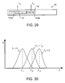
- FIG. 29 A diagram of an illustrative tunable source 64 based on two grating regions that are independently controlled is shown in FIG. 29 .
- the periodicity of the grating 110 underlying each pad 102 may be different, which allows either grating region to be activated by applying the appropriate drive current to pads 102 .
- a current I 1 may be applied to region 64 when it is desired to create gain under pad 102 a .
- a current I 2 may be applied to region 64 when it is desired to create gain under pad 102 b.
- the resulting gain spectra for source region 64 of FIG. 29 for various different combinations of currents I 1 , and I 2 is shown in FIG. 30 .
- the wavelength of light that is produced by the tunable source of FIG. 29 depends on the relative drive currents for each of the independently-controllable portions of source region 64 of FIG. 29 .
- each tunable source region 64 may be based on a grating 110 with a different periodicity or with the same periodicity.
- Light may be generated by source region 64 a by applying current to a portion of source region 64 a through contact pad 102 - 3 .
- Light may be generated by source region 64 b by applying current through contact 102 - 4 .
- the wavelengths of light that are generated by source regions 64 a and 64 b are determined by the periodicity of the corresponding grating 110 .
- the wavelengths of light that are generated by source regions 64 a and 64 b can be tuned by adjusting the current applied through pads 102 - 1 and 102 - 2 , respectively.
- Source regions 64 Although structures such as device 62 of FIG. 31 are shown with only two source regions 64 , this is merely illustrative. Any suitable number of source regions 64 may be provided if desired.
- Source region 64 may be one of source regions 64 a and 64 b in FIG. 31 or may be one of a group of source regions, each of which has a grating 110 with the same periodicity.
- a current J may be applied in the vicinity of grating 110 .
- the magnitude of current J may be adjusted to alter the index of refraction surrounding grating 110 so that light at either wavelength ⁇ 1 or ⁇ 2 is coupled from waveguide layer 128 into waveguide layer 130 by grating 110 .
- Residual light that is passing through layer 128 past grating 110 in direction 132 at the desired and undesired wavelengths is absorbed by layer 128 , because layer 128 provides optical absorption in the absence of current J.
- the light at the desired wavelength ( ⁇ 1 or ⁇ 2 ) that is coupled into waveguide layer 130 is reflected back in direction 134 by reflective coating 100 , because waveguide 130 does not absorb light at wavelengths ⁇ 1 and ⁇ 2 .
- grating 110 couples this light back from layer 130 into layer 128 .
- This light may exit device 62 through antireflection coating 98 (or other suitable low-reflectivity coating), as indicated by arrow 136 .
- the spectra produced by pump 20 may be adjusted by controlling the thicknesses and material compositions of the multiple quantum wells or other structures in each source region 64 .
- a graph of an illustrative gain spectrum that may be produced by an active region in a region 64 that includes three different groups of multiple quantum wells is shown in FIG. 33.
- a region 64 with the spectrum of FIG. 33 may be tuned to produce light at a wavelength of ⁇ 1 , ⁇ 2 , or ⁇ 3 .
- ⁇ 33 may therefore be used as the active layer in a device 62 having source regions 64 each of which has a grating or other structure that restricts the emitted light that is associated with that source region 64 to ⁇ 1 , ⁇ 2 , or ⁇ 3 , respectively.
- An external cavity or coupled-cavity arrangement may be used to selectively produce pump light at different pump wavelengths, as shown in FIG. 34 .
- light from device 62 is coupled into a fiber 138 having gratings 140 and 142 by optical coupler 72 (e.g., a lens or an optical coupler that is integral with the tip of fiber 138 ).
- Gratings 140 and 142 e.g., fiber Bragg gratings
- Multiplexer 68 directs light at each wavelength into an appropriate source region 64 .
- Light exiting each source region 64 is coupled into waveguide 66 by multiplexer 68 .
- FIG. 35 A graph showing how the arrangement of FIG. 34 may be used to ensure that Raman pump 20 produces pump light at the wavelengths ⁇ 1 , and ⁇ 2 determined by the gratings 140 and 142 is shown in FIG. 35 .
- the spectrum labeled MUX 1 corresponds to the multiplexer pass band associated with a first leg 151 of multiplexer 68 (or a set of such legs).
- the spectrum labeled MUX 2 corresponds to the pass band of a second leg 152 of multiplexer 68 (or a set of such legs).
- gratings 140 and 142 have bandwidths of ⁇ about the desired wavelengths ⁇ 1 , and ⁇ 2 . These wavelengths lie within the pass bands of the legs of multiplexer 68 .
- the wavelength selectivity of filters 140 and 142 and the wavelength selectivity of multiplexer 68 the light produced by source regions 64 a and 64 b and therefore by pump 20 is centered around ⁇ 1 and ⁇ 2 with bandwidths ⁇ .
- Semiconductor patterning techniques may be used to manufacture wafers of devices 62 with different source regions 64 .
- An example is shown in FIG. 36.
- a pattern may be formed on wafer 144 that opens mask holes 144 overlying source regions 64 - 1 .
- holes 144 may be covered and holes 146 may be opened that overlie source regions 64 - 2 .
- Gratings 110 of a different periodicity than the gratings 110 formed through holes 144 may then be formed. This approach may be repeated to form any suitable number of source regions 64 having different gratings or other structures. Any suitable masking techniques may be used to form mask holes such as holes 144 and 146 .
- holes may be formed in mask layers formed from oxides, glasses, photoresists, metals, polymers, etc.
- FIG. 36 is merely illustrative. Any suitable semiconductor fabrication techniques may be used to pattern the waveguides, gratings, contact pads, and other structures associated with devices 62 of pumps 20 .
Abstract
Description
Claims (4)
Priority Applications (1)
| Application Number | Priority Date | Filing Date | Title |
|---|---|---|---|
| US09/783,395 US6433921B1 (en) | 2001-01-12 | 2001-02-15 | Multiwavelength pumps for raman amplifier systems |
Applications Claiming Priority (2)
| Application Number | Priority Date | Filing Date | Title |
|---|---|---|---|
| US26088401P | 2001-01-12 | 2001-01-12 | |
| US09/783,395 US6433921B1 (en) | 2001-01-12 | 2001-02-15 | Multiwavelength pumps for raman amplifier systems |
Publications (1)
| Publication Number | Publication Date |
|---|---|
| US6433921B1 true US6433921B1 (en) | 2002-08-13 |
Family
ID=26948243
Family Applications (1)
| Application Number | Title | Priority Date | Filing Date |
|---|---|---|---|
| US09/783,395 Expired - Lifetime US6433921B1 (en) | 2001-01-12 | 2001-02-15 | Multiwavelength pumps for raman amplifier systems |
Country Status (1)
| Country | Link |
|---|---|
| US (1) | US6433921B1 (en) |
Cited By (52)
| Publication number | Priority date | Publication date | Assignee | Title |
|---|---|---|---|---|
| US20020102051A1 (en) * | 2001-01-31 | 2002-08-01 | Sumitomo Electric Industries, Ltd. | Optical communication system |
| US20020154390A1 (en) * | 2001-04-20 | 2002-10-24 | William Shieh | Pump assembly employing coupled radiation sources for multiple fibers |
| US20020181515A1 (en) * | 2001-05-31 | 2002-12-05 | Kennet Vilhemsson | Apparatus and method for controlling the operating wavelength of a laser diode |
| WO2002103402A2 (en) * | 2001-06-18 | 2002-12-27 | Orchid Lightwave Communications, Inc. | Electro-optic waveguide modulator method and apparatus |
| US6501886B1 (en) * | 2001-07-30 | 2002-12-31 | Agilent Technologies, Inc. | Compact optical splitter and combiner |
| US20030030890A1 (en) * | 2001-08-10 | 2003-02-13 | Fujitsu Limited | Raman amplifier |
| US6532101B2 (en) * | 2001-03-16 | 2003-03-11 | Xtera Communications, Inc. | System and method for wide band Raman amplification |
| US20030058899A1 (en) * | 1996-12-23 | 2003-03-27 | Xtera Communications, Inc., A Delaware Corporation | Optical amplification using polarization diversity pumping |
| US6577789B1 (en) * | 2001-09-26 | 2003-06-10 | Onetta, Inc. | Double-pass optical amplifiers and optical network equipment |
| US6600592B2 (en) * | 1998-03-24 | 2003-07-29 | Xtera Communications, Inc. | S+ band nonlinear polarization amplifiers |
| US6611370B2 (en) * | 1999-07-23 | 2003-08-26 | The Furukawa Electric Co., Ltd. | Raman amplifier system, apparatus and method for identifying, obtaining and maintaining an arbitrary Raman amplification performance |
| US20030174954A1 (en) * | 2002-03-14 | 2003-09-18 | Nec Corporation | Multi-mode interference waveguide-including semiconductor laser diode module, fiber-type optical amplifier, optical relay and optical communication system |
| US20030184846A1 (en) * | 2002-03-27 | 2003-10-02 | Bennett Kevin W. | Modular optical amplifier assembly and a method of assembly |
| US20030206336A1 (en) * | 2002-05-02 | 2003-11-06 | Fujitsu Limited | Variable wavelength light source apparatus and optical amplifier using same |
| US6646786B1 (en) | 2002-05-06 | 2003-11-11 | Cisco Technology, Inc. | Copropagating Raman pump unit to suppress four-wave mixing crosstalk between pump modes and WDM signals |
| US20030210913A1 (en) * | 2002-03-01 | 2003-11-13 | Motoki Kakui | Light generator, optical amplifier, and optical communication system |
| US20030210457A1 (en) * | 2002-03-15 | 2003-11-13 | The Furukawa Electric Co., Ltd. | Tunable multimode wavelength division multiplex raman pump and amplifier, and a system, method, and computer program product for controlling tunable raman pumps, and raman amplifiers |
| US6724791B1 (en) * | 2002-07-02 | 2004-04-20 | C-Cor.Net Corp. | Method and apparatus for controlling the temperature of a laser module in fiber optic transmissions |
| US6731425B1 (en) * | 2002-03-07 | 2004-05-04 | Cisco Technology, Inc. | Modular Raman pump double-multiplexer |
| US6768577B2 (en) * | 2002-03-15 | 2004-07-27 | Fitel Usa Corp. | Tunable multimode laser diode module, tunable multimode wavelength division multiplex raman pump, and amplifier, and a system, method, and computer program product for controlling tunable multimode laser diodes, raman pumps, and raman amplifiers |
| US6775055B2 (en) * | 2000-07-21 | 2004-08-10 | Sumitomo Electric Industries, Ltd. | Raman amplifier |
| US20040184816A1 (en) * | 2003-03-19 | 2004-09-23 | Alcatel | Multiwavelength depolarized Raman pumps |
| US6798945B1 (en) * | 2001-08-30 | 2004-09-28 | Cisco Technology, Inc. | Lumped raman amplifier for adaptive dispersion compensation |
| US6806999B2 (en) | 2001-12-06 | 2004-10-19 | Sumitomo Electric Industries, Ltd. | Raman amplification pumping module, Raman amplifier, and optical communication system |
| US6823107B2 (en) * | 2001-09-28 | 2004-11-23 | Fujitsu Limited | Method and device for optical amplification |
| US6831777B2 (en) * | 2001-02-07 | 2004-12-14 | Fujitsu Limited | Optical transmission system and method |
| US6859469B2 (en) * | 2001-12-11 | 2005-02-22 | Adc Telecommunications, Inc. | Method and apparatus for laser wavelength stabilization |
| US6867907B2 (en) * | 2001-06-29 | 2005-03-15 | Sumitomo Electric Industries, Ltd. | Pumping light source unit, raman amplifier, and optical transmission system |
| US6867905B1 (en) * | 2001-03-28 | 2005-03-15 | Cisco Technolog, Inc. | Reduced four-wave mixing and raman amplification architecture |
| US20050057794A1 (en) * | 2001-02-23 | 2005-03-17 | Fujitsu Limited | Raman excitation control method and optical transmission system using the same |
| US20050088725A1 (en) * | 2000-03-02 | 2005-04-28 | Nec Corporation | Optical amplifier, optical amplifying repeater and transmission apparatus of wavelength division multiplexed signal light using the same |
| US20050105165A1 (en) * | 2003-09-08 | 2005-05-19 | The Furukawa Electric Co., Ltd. | Raman amplifier, pump source for use in a raman amplifier and method for amplifying an optical signal |
| US20050135738A1 (en) * | 2003-12-23 | 2005-06-23 | Hyun-Cheol Shin | Broadband light source and broadband optical module using the same |
| FR2864358A1 (en) * | 2003-12-18 | 2005-06-24 | Saint Louis Inst | Infrared radiation generating device for e.g. use on aircraft, has diode emitting laser radiation in specific frequency range, and control unit controlling diode temperature to control wavelength of radiation emitted by diode |
| US6937389B1 (en) * | 2001-12-13 | 2005-08-30 | Corvis Corporation | Optical communication systems and optical amplifiers employing periodic combiners and methods |
| US20050265647A1 (en) * | 2002-08-02 | 2005-12-01 | Daryoosh Vakhshoori | System for amplifying optical signals |
| US6977769B2 (en) * | 2001-01-31 | 2005-12-20 | The Furukawa Electric Co., Ltd. | Pump light source device for optical Raman amplification and optical Raman amplification system using the same |
| US7038782B2 (en) | 2001-12-11 | 2006-05-02 | Adc Telecommunications, Inc. | Robust wavelength locker for control of laser wavelength |
| US7054059B1 (en) | 2003-05-14 | 2006-05-30 | Cisco Technoloy, Inc. | Lumped Raman amplification structure for very wideband applications |
| US7075656B2 (en) | 2001-12-11 | 2006-07-11 | Adc Telecommunications, Inc. | Method and algorithm for continuous wavelength locking |
| US20060159149A1 (en) * | 2005-01-18 | 2006-07-20 | Sanmina-Sci Corporation | Systems and methods for optical pumping using depolarizing filters |
| US7181095B1 (en) | 2003-07-29 | 2007-02-20 | Cisco Technology, Inc. | Low loss, noise filtering multiplexer/demultiplexer for reconfigurable OADMs |
| US20070058243A1 (en) * | 2003-03-12 | 2007-03-15 | Daryoosh Vakhshoori | Extended optical bandwidth semiconductor source |
| KR100749815B1 (en) | 2005-09-15 | 2007-08-16 | 주식회사 와이텔포토닉스 | Broadband Source System using several multi-wavelength superluminescent diode chips and 1×N optical fiber coupler |
| GB2436408A (en) * | 2006-03-21 | 2007-09-26 | Azea Networks Ltd | Depolarising a WDM signal by passing it through a differential group delay element |
| US20080157887A1 (en) * | 2005-02-14 | 2008-07-03 | Patrick Berthoud | Optical Pumping Device And Method |
| US20090323174A1 (en) * | 2004-08-11 | 2009-12-31 | Siemens Aktiengesellschaft | Method and arrangement for the rapid adjustment of the tilt of optical wdm signals |
| US20120002283A1 (en) * | 2010-06-30 | 2012-01-05 | Chongjin Xie | Method and apparatus for raman co-pumps |
| US20150015953A1 (en) * | 2012-02-28 | 2015-01-15 | Accelink Technologies Co., Ltd. | Single-pump multi-wavelength lasing semiconductor raman pump laser and pump combination apparatus |
| CN104641212A (en) * | 2012-06-29 | 2015-05-20 | 贰陆股份公司 | Method and apparatus for determining optical fibre characteristics |
| US20150340829A1 (en) * | 2013-02-08 | 2015-11-26 | Carl Zeiss Smt Gmbh | Beam Reverser Module and Optical Power Amplifier Having Such a Beam Reverser Module |
| US10523334B1 (en) * | 2018-12-07 | 2019-12-31 | Fujitsu Limited | Controlling gain modulation in optical communication networks |
Citations (40)
| Publication number | Priority date | Publication date | Assignee | Title |
|---|---|---|---|---|
| US4379289A (en) | 1979-03-08 | 1983-04-05 | Gte Laboratories Incorporated | Fiber optics security system |
| US4651317A (en) | 1982-11-24 | 1987-03-17 | Hitachi, Ltd. | Time division multiplex data transmission system |
| US4745612A (en) | 1985-07-16 | 1988-05-17 | Sharp Kabushiki Kaisha | Separate confinement heterostructure semiconductor laser device |
| US4881790A (en) | 1988-04-25 | 1989-11-21 | American Telephone And Telegraph Company, At&T Bell Laboratories | Optical communications system comprising raman amplification means |
| US5039194A (en) | 1990-01-09 | 1991-08-13 | International Business Machines Corporation | Optical fiber link card |
| US5136410A (en) | 1990-01-09 | 1992-08-04 | Ibm Corporation | Optical fiber link control safety system |
| US5189679A (en) | 1991-09-06 | 1993-02-23 | The Boeing Company | Strained quantum well laser for high temperature operation |
| US5208183A (en) | 1990-12-20 | 1993-05-04 | At&T Bell Laboratories | Method of making a semiconductor laser |
| US5218613A (en) | 1992-05-01 | 1993-06-08 | Mcdonnell Douglas Corporation | Visible diode laser |
| US5287377A (en) | 1991-12-16 | 1994-02-15 | International Business Machines Corporation | Coupled quantum well tunable laser |
| US5345456A (en) | 1993-03-11 | 1994-09-06 | National Research Council Of Canada | Spatially addressable surface emission sum frequency device |
| US5428471A (en) | 1992-07-30 | 1995-06-27 | Alcatel Network Systems, Inc. | Fail-safe automatic shut-down apparatus and method for high output power optical communications system |
| US5430759A (en) | 1992-08-20 | 1995-07-04 | Nexus 1994 Limited | Low-power frequency-hopped spread spectrum reverse paging system |
| US5623508A (en) | 1996-02-12 | 1997-04-22 | Lucent Technologies Inc. | Article comprising a counter-pumped optical fiber raman amplifier |
| US5673280A (en) | 1996-02-12 | 1997-09-30 | Lucent Technologies Inc. | Article comprising low noise optical fiber raman amplifier |
| US5920423A (en) * | 1997-12-05 | 1999-07-06 | Sdl, Inc. | Multiple pumped fiber amplifiers for WDM communication systems with adjustment for the amplifier signal gain bandwidth |
| US5936763A (en) * | 1996-11-15 | 1999-08-10 | Matsushita Electric Industrial Co., Ltd. | Optical fiber amplifier, semiconductor laser module for pumping and optical signal communication system |
| US5945668A (en) | 1997-06-20 | 1999-08-31 | Sun Microsystems, Inc. | Fiber optic system with open fiber safety interlock |
| US5946129A (en) | 1996-09-05 | 1999-08-31 | Oki Electric Industry Co., Ltd. | Wavelength conversion apparatus with improved efficiency, easy adjustability, and polarization insensitivity |
| US5959750A (en) | 1996-06-06 | 1999-09-28 | Lucent Technologies Inc. | Method of upgrading transmission capacity by Raman amplification |
| WO1999066607A2 (en) | 1998-06-16 | 1999-12-23 | Xtera Communications, Inc. | Fiber-optic compensation for dispersion, gain tilt, and band pump nonlinearity |
| US6014235A (en) | 1997-06-03 | 2000-01-11 | Lucent Technologies Inc. | Optical-loop buffer that enhances the extinction ratio of the buffered signal |
| US6028875A (en) | 1996-10-11 | 2000-02-22 | Nortel Networks Corporation | Buried heterostructure laser with quaternary current blocking layer |
| US6052222A (en) | 1996-12-26 | 2000-04-18 | Nec Corporation | Semiconductor optical amplifier |
| US6052393A (en) | 1996-12-23 | 2000-04-18 | The Regents Of The University Of Michigan | Broadband Sagnac Raman amplifiers and cascade lasers |
| WO2000049721A2 (en) | 1999-02-19 | 2000-08-24 | Corvis Corporation | Optical transmission systems including signal varying devices and methods |
| US6115174A (en) | 1998-07-21 | 2000-09-05 | Corvis Corporation | Optical signal varying devices |
| US6122306A (en) | 1995-03-31 | 2000-09-19 | Heinrich-Hertz-Institut Fuer Nachrichtentechnik Berlin Gmbh | Self-pulsing multi-section laser |
| US6141477A (en) | 1997-01-10 | 2000-10-31 | Nec Corporation | Semiconductor optical amplification element |
| US6147794A (en) | 1999-02-04 | 2000-11-14 | Lucent Technologies, Inc. | Raman amplifier with pump source for improved performance |
| US6151160A (en) | 1998-10-05 | 2000-11-21 | Tyco Submarine Systems Ltd. | Broadband Raman pre-amplifier for wavelength division multiplexed optical communication systems |
| WO2000073849A1 (en) | 1999-05-31 | 2000-12-07 | The Furukawa Electric Co., Ltd. | Raman amplification system and optical signal transmission method using the same |
| US6163636A (en) | 1999-01-19 | 2000-12-19 | Lucent Technologies Inc. | Optical communication system using multiple-order Raman amplifiers |
| US6178038B1 (en) | 1998-02-20 | 2001-01-23 | Ciena Corporation | Optical amplifier having an improved noise figure |
| US6181464B1 (en) | 1998-12-01 | 2001-01-30 | Tycom (Us) Inc. | Low noise Raman amplifier employing bidirectional pumping and an optical transmission system incorporating same |
| US6192058B1 (en) | 1998-09-18 | 2001-02-20 | Sarnoff Corporation | Multiwavelength actively mode-locked external cavity semiconductor laser |
| US6215805B1 (en) | 1996-03-29 | 2001-04-10 | Heinrich-Hertz-Institut Fuer Nachrichtentechnik Berlin Gmbh | Q-switched semiconductor laser |
| US6275313B1 (en) | 1998-02-03 | 2001-08-14 | Lucent Technologies Inc. | Raman gain tilt equalization in optical fiber communication systems |
| US6292288B1 (en) * | 1998-07-23 | 2001-09-18 | The Furukawa Electric Co., Ltd. | Raman amplifier, optical repeater, and raman amplification method |
| US6320695B1 (en) * | 1999-01-14 | 2001-11-20 | The Furukawa Electric Co., Ltd. | Optical amplifying apparatus |
-
2001
- 2001-02-15 US US09/783,395 patent/US6433921B1/en not_active Expired - Lifetime
Patent Citations (40)
| Publication number | Priority date | Publication date | Assignee | Title |
|---|---|---|---|---|
| US4379289A (en) | 1979-03-08 | 1983-04-05 | Gte Laboratories Incorporated | Fiber optics security system |
| US4651317A (en) | 1982-11-24 | 1987-03-17 | Hitachi, Ltd. | Time division multiplex data transmission system |
| US4745612A (en) | 1985-07-16 | 1988-05-17 | Sharp Kabushiki Kaisha | Separate confinement heterostructure semiconductor laser device |
| US4881790A (en) | 1988-04-25 | 1989-11-21 | American Telephone And Telegraph Company, At&T Bell Laboratories | Optical communications system comprising raman amplification means |
| US5039194A (en) | 1990-01-09 | 1991-08-13 | International Business Machines Corporation | Optical fiber link card |
| US5136410A (en) | 1990-01-09 | 1992-08-04 | Ibm Corporation | Optical fiber link control safety system |
| US5208183A (en) | 1990-12-20 | 1993-05-04 | At&T Bell Laboratories | Method of making a semiconductor laser |
| US5189679A (en) | 1991-09-06 | 1993-02-23 | The Boeing Company | Strained quantum well laser for high temperature operation |
| US5287377A (en) | 1991-12-16 | 1994-02-15 | International Business Machines Corporation | Coupled quantum well tunable laser |
| US5218613A (en) | 1992-05-01 | 1993-06-08 | Mcdonnell Douglas Corporation | Visible diode laser |
| US5428471A (en) | 1992-07-30 | 1995-06-27 | Alcatel Network Systems, Inc. | Fail-safe automatic shut-down apparatus and method for high output power optical communications system |
| US5430759A (en) | 1992-08-20 | 1995-07-04 | Nexus 1994 Limited | Low-power frequency-hopped spread spectrum reverse paging system |
| US5345456A (en) | 1993-03-11 | 1994-09-06 | National Research Council Of Canada | Spatially addressable surface emission sum frequency device |
| US6122306A (en) | 1995-03-31 | 2000-09-19 | Heinrich-Hertz-Institut Fuer Nachrichtentechnik Berlin Gmbh | Self-pulsing multi-section laser |
| US5673280A (en) | 1996-02-12 | 1997-09-30 | Lucent Technologies Inc. | Article comprising low noise optical fiber raman amplifier |
| US5623508A (en) | 1996-02-12 | 1997-04-22 | Lucent Technologies Inc. | Article comprising a counter-pumped optical fiber raman amplifier |
| US6215805B1 (en) | 1996-03-29 | 2001-04-10 | Heinrich-Hertz-Institut Fuer Nachrichtentechnik Berlin Gmbh | Q-switched semiconductor laser |
| US5959750A (en) | 1996-06-06 | 1999-09-28 | Lucent Technologies Inc. | Method of upgrading transmission capacity by Raman amplification |
| US5946129A (en) | 1996-09-05 | 1999-08-31 | Oki Electric Industry Co., Ltd. | Wavelength conversion apparatus with improved efficiency, easy adjustability, and polarization insensitivity |
| US6028875A (en) | 1996-10-11 | 2000-02-22 | Nortel Networks Corporation | Buried heterostructure laser with quaternary current blocking layer |
| US5936763A (en) * | 1996-11-15 | 1999-08-10 | Matsushita Electric Industrial Co., Ltd. | Optical fiber amplifier, semiconductor laser module for pumping and optical signal communication system |
| US6052393A (en) | 1996-12-23 | 2000-04-18 | The Regents Of The University Of Michigan | Broadband Sagnac Raman amplifiers and cascade lasers |
| US6052222A (en) | 1996-12-26 | 2000-04-18 | Nec Corporation | Semiconductor optical amplifier |
| US6141477A (en) | 1997-01-10 | 2000-10-31 | Nec Corporation | Semiconductor optical amplification element |
| US6014235A (en) | 1997-06-03 | 2000-01-11 | Lucent Technologies Inc. | Optical-loop buffer that enhances the extinction ratio of the buffered signal |
| US5945668A (en) | 1997-06-20 | 1999-08-31 | Sun Microsystems, Inc. | Fiber optic system with open fiber safety interlock |
| US5920423A (en) * | 1997-12-05 | 1999-07-06 | Sdl, Inc. | Multiple pumped fiber amplifiers for WDM communication systems with adjustment for the amplifier signal gain bandwidth |
| US6275313B1 (en) | 1998-02-03 | 2001-08-14 | Lucent Technologies Inc. | Raman gain tilt equalization in optical fiber communication systems |
| US6178038B1 (en) | 1998-02-20 | 2001-01-23 | Ciena Corporation | Optical amplifier having an improved noise figure |
| WO1999066607A2 (en) | 1998-06-16 | 1999-12-23 | Xtera Communications, Inc. | Fiber-optic compensation for dispersion, gain tilt, and band pump nonlinearity |
| US6115174A (en) | 1998-07-21 | 2000-09-05 | Corvis Corporation | Optical signal varying devices |
| US6292288B1 (en) * | 1998-07-23 | 2001-09-18 | The Furukawa Electric Co., Ltd. | Raman amplifier, optical repeater, and raman amplification method |
| US6192058B1 (en) | 1998-09-18 | 2001-02-20 | Sarnoff Corporation | Multiwavelength actively mode-locked external cavity semiconductor laser |
| US6151160A (en) | 1998-10-05 | 2000-11-21 | Tyco Submarine Systems Ltd. | Broadband Raman pre-amplifier for wavelength division multiplexed optical communication systems |
| US6181464B1 (en) | 1998-12-01 | 2001-01-30 | Tycom (Us) Inc. | Low noise Raman amplifier employing bidirectional pumping and an optical transmission system incorporating same |
| US6320695B1 (en) * | 1999-01-14 | 2001-11-20 | The Furukawa Electric Co., Ltd. | Optical amplifying apparatus |
| US6163636A (en) | 1999-01-19 | 2000-12-19 | Lucent Technologies Inc. | Optical communication system using multiple-order Raman amplifiers |
| US6147794A (en) | 1999-02-04 | 2000-11-14 | Lucent Technologies, Inc. | Raman amplifier with pump source for improved performance |
| WO2000049721A2 (en) | 1999-02-19 | 2000-08-24 | Corvis Corporation | Optical transmission systems including signal varying devices and methods |
| WO2000073849A1 (en) | 1999-05-31 | 2000-12-07 | The Furukawa Electric Co., Ltd. | Raman amplification system and optical signal transmission method using the same |
Non-Patent Citations (27)
Cited By (93)
| Publication number | Priority date | Publication date | Assignee | Title |
|---|---|---|---|---|
| US20030058899A1 (en) * | 1996-12-23 | 2003-03-27 | Xtera Communications, Inc., A Delaware Corporation | Optical amplification using polarization diversity pumping |
| US6833946B2 (en) * | 1996-12-23 | 2004-12-21 | Xtera Communications, Inc. | Optical amplification using polarization diversity pumping |
| US6600592B2 (en) * | 1998-03-24 | 2003-07-29 | Xtera Communications, Inc. | S+ band nonlinear polarization amplifiers |
| US20040032641A1 (en) * | 1999-07-23 | 2004-02-19 | The Furukawa Electric Co., Ltd. | Raman amplifier system, apparatus and method for identifying, obtaining and maintaining an arbitrary raman amplification performance |
| US6917466B2 (en) | 1999-07-23 | 2005-07-12 | The Furukawa Electric Co., Ltd. | Raman amplifier system, apparatus and method for identifying, obtaining and maintaining an arbitrary Raman amplification performance |
| US6611370B2 (en) * | 1999-07-23 | 2003-08-26 | The Furukawa Electric Co., Ltd. | Raman amplifier system, apparatus and method for identifying, obtaining and maintaining an arbitrary Raman amplification performance |
| US20050088725A1 (en) * | 2000-03-02 | 2005-04-28 | Nec Corporation | Optical amplifier, optical amplifying repeater and transmission apparatus of wavelength division multiplexed signal light using the same |
| US6775055B2 (en) * | 2000-07-21 | 2004-08-10 | Sumitomo Electric Industries, Ltd. | Raman amplifier |
| US7046428B2 (en) * | 2000-07-21 | 2006-05-16 | Sumitomo Electric Industries, Ltd. | Raman amplifier |
| US20040240039A1 (en) * | 2000-07-21 | 2004-12-02 | Sumitomo Electric Industries, Ltd. | Raman amplifier |
| US6819829B2 (en) | 2001-01-31 | 2004-11-16 | Sumitomo Electric Industries, Ltd. | Optical communication system |
| US6977769B2 (en) * | 2001-01-31 | 2005-12-20 | The Furukawa Electric Co., Ltd. | Pump light source device for optical Raman amplification and optical Raman amplification system using the same |
| US20020102051A1 (en) * | 2001-01-31 | 2002-08-01 | Sumitomo Electric Industries, Ltd. | Optical communication system |
| US6831777B2 (en) * | 2001-02-07 | 2004-12-14 | Fujitsu Limited | Optical transmission system and method |
| US20050057794A1 (en) * | 2001-02-23 | 2005-03-17 | Fujitsu Limited | Raman excitation control method and optical transmission system using the same |
| US6532101B2 (en) * | 2001-03-16 | 2003-03-11 | Xtera Communications, Inc. | System and method for wide band Raman amplification |
| US6646788B2 (en) | 2001-03-16 | 2003-11-11 | Xtera Communications, Inc. | System and method for wide band Raman amplification |
| US6867905B1 (en) * | 2001-03-28 | 2005-03-15 | Cisco Technolog, Inc. | Reduced four-wave mixing and raman amplification architecture |
| US20050157378A1 (en) * | 2001-03-28 | 2005-07-21 | Cisco Technology, Inc. | Reduced four-wave mixing and raman amplification architecture |
| US7038842B2 (en) | 2001-03-28 | 2006-05-02 | Cisco Technology, Inc. | Reduced four-wave mixing and Raman amplification architecture |
| US6618195B2 (en) * | 2001-04-20 | 2003-09-09 | Dorsal Networks Inc. | Pump assembly employing coupled radiation sources for multiple fibers |
| US20020154390A1 (en) * | 2001-04-20 | 2002-10-24 | William Shieh | Pump assembly employing coupled radiation sources for multiple fibers |
| US20040042064A1 (en) * | 2001-04-20 | 2004-03-04 | Dorsal Networks, Inc. | Pump assembly employing coupled radiation sources for multiple fibers |
| US6894831B2 (en) | 2001-04-20 | 2005-05-17 | Dorsal Networks, Inc. | Pump assembly employing coupled radiation sources for multiple fibers |
| US20020181515A1 (en) * | 2001-05-31 | 2002-12-05 | Kennet Vilhemsson | Apparatus and method for controlling the operating wavelength of a laser diode |
| WO2002103402A3 (en) * | 2001-06-18 | 2004-03-18 | Orchid Lightwave Communication | Electro-optic waveguide modulator method and apparatus |
| WO2002103402A2 (en) * | 2001-06-18 | 2002-12-27 | Orchid Lightwave Communications, Inc. | Electro-optic waveguide modulator method and apparatus |
| US6867907B2 (en) * | 2001-06-29 | 2005-03-15 | Sumitomo Electric Industries, Ltd. | Pumping light source unit, raman amplifier, and optical transmission system |
| US6501886B1 (en) * | 2001-07-30 | 2002-12-31 | Agilent Technologies, Inc. | Compact optical splitter and combiner |
| US6954304B2 (en) * | 2001-08-10 | 2005-10-11 | Fujitsu Limited | Raman amplifier |
| US20030030890A1 (en) * | 2001-08-10 | 2003-02-13 | Fujitsu Limited | Raman amplifier |
| US7231108B2 (en) * | 2001-08-30 | 2007-06-12 | Cisco Technology, Inc. | Lumped raman amplifier for adaptive dispersion compensation |
| US7024071B1 (en) | 2001-08-30 | 2006-04-04 | Cisco Technology, Inc. | Lumped Raman amplifier for adaptive dispersion compensation |
| US6798945B1 (en) * | 2001-08-30 | 2004-09-28 | Cisco Technology, Inc. | Lumped raman amplifier for adaptive dispersion compensation |
| US20060126998A1 (en) * | 2001-08-30 | 2006-06-15 | Cisco Technology, Inc. | Lumped raman amplifier for adaptive dispersion compensation |
| US6577789B1 (en) * | 2001-09-26 | 2003-06-10 | Onetta, Inc. | Double-pass optical amplifiers and optical network equipment |
| US6823107B2 (en) * | 2001-09-28 | 2004-11-23 | Fujitsu Limited | Method and device for optical amplification |
| US6806999B2 (en) | 2001-12-06 | 2004-10-19 | Sumitomo Electric Industries, Ltd. | Raman amplification pumping module, Raman amplifier, and optical communication system |
| US6859469B2 (en) * | 2001-12-11 | 2005-02-22 | Adc Telecommunications, Inc. | Method and apparatus for laser wavelength stabilization |
| US7075656B2 (en) | 2001-12-11 | 2006-07-11 | Adc Telecommunications, Inc. | Method and algorithm for continuous wavelength locking |
| US7038782B2 (en) | 2001-12-11 | 2006-05-02 | Adc Telecommunications, Inc. | Robust wavelength locker for control of laser wavelength |
| US6937389B1 (en) * | 2001-12-13 | 2005-08-30 | Corvis Corporation | Optical communication systems and optical amplifiers employing periodic combiners and methods |
| US7580183B2 (en) * | 2002-03-01 | 2009-08-25 | Sumitomo Electric Industries, Ltd. | Light generator, optical amplifier, and optical communication system |
| US20030210913A1 (en) * | 2002-03-01 | 2003-11-13 | Motoki Kakui | Light generator, optical amplifier, and optical communication system |
| US6731425B1 (en) * | 2002-03-07 | 2004-05-04 | Cisco Technology, Inc. | Modular Raman pump double-multiplexer |
| US20030174954A1 (en) * | 2002-03-14 | 2003-09-18 | Nec Corporation | Multi-mode interference waveguide-including semiconductor laser diode module, fiber-type optical amplifier, optical relay and optical communication system |
| US6768577B2 (en) * | 2002-03-15 | 2004-07-27 | Fitel Usa Corp. | Tunable multimode laser diode module, tunable multimode wavelength division multiplex raman pump, and amplifier, and a system, method, and computer program product for controlling tunable multimode laser diodes, raman pumps, and raman amplifiers |
| US7199919B2 (en) * | 2002-03-15 | 2007-04-03 | The Furukawa Electric Co., Ltd. | Tunable multimode wavelength division multiplex Raman pump and amplifier, and a system, method, and computer program product for controlling tunable Raman pumps, and Raman amplifiers |
| US20030210457A1 (en) * | 2002-03-15 | 2003-11-13 | The Furukawa Electric Co., Ltd. | Tunable multimode wavelength division multiplex raman pump and amplifier, and a system, method, and computer program product for controlling tunable raman pumps, and raman amplifiers |
| US20030184846A1 (en) * | 2002-03-27 | 2003-10-02 | Bennett Kevin W. | Modular optical amplifier assembly and a method of assembly |
| US6741390B2 (en) * | 2002-05-02 | 2004-05-25 | Fujitsu Limited | Variable wavelength light source apparatus and optical amplifier using same |
| US20030206336A1 (en) * | 2002-05-02 | 2003-11-06 | Fujitsu Limited | Variable wavelength light source apparatus and optical amplifier using same |
| US6646786B1 (en) | 2002-05-06 | 2003-11-11 | Cisco Technology, Inc. | Copropagating Raman pump unit to suppress four-wave mixing crosstalk between pump modes and WDM signals |
| US6724791B1 (en) * | 2002-07-02 | 2004-04-20 | C-Cor.Net Corp. | Method and apparatus for controlling the temperature of a laser module in fiber optic transmissions |
| US20050265647A1 (en) * | 2002-08-02 | 2005-12-01 | Daryoosh Vakhshoori | System for amplifying optical signals |
| US7215836B2 (en) * | 2002-08-02 | 2007-05-08 | Ahura Corporation | System for amplifying optical signals |
| US20070058243A1 (en) * | 2003-03-12 | 2007-03-15 | Daryoosh Vakhshoori | Extended optical bandwidth semiconductor source |
| US20040184816A1 (en) * | 2003-03-19 | 2004-09-23 | Alcatel | Multiwavelength depolarized Raman pumps |
| US7054059B1 (en) | 2003-05-14 | 2006-05-30 | Cisco Technoloy, Inc. | Lumped Raman amplification structure for very wideband applications |
| US7692850B1 (en) | 2003-05-14 | 2010-04-06 | Cisco Technology, Inc. | Lumped-Raman amplification structure for very wideband applications |
| US7706643B1 (en) | 2003-07-29 | 2010-04-27 | Cisco Technology, Inc. | Low loss, noise filtering multiplexer/demultiplexer for reconfigurable OADMs |
| US7181095B1 (en) | 2003-07-29 | 2007-02-20 | Cisco Technology, Inc. | Low loss, noise filtering multiplexer/demultiplexer for reconfigurable OADMs |
| US7542634B1 (en) | 2003-07-29 | 2009-06-02 | Cisco Technology, Inc. | Low loss, noise filtering multiplexer/demultiplexer for reconfigurable OADMs |
| US20050105165A1 (en) * | 2003-09-08 | 2005-05-19 | The Furukawa Electric Co., Ltd. | Raman amplifier, pump source for use in a raman amplifier and method for amplifying an optical signal |
| US7206123B2 (en) | 2003-09-08 | 2007-04-17 | The Furukawa Electric Co. Ltd. | Raman amplifier, pump source for use in a raman amplifier and method for amplifying an optical signal |
| FR2866488A1 (en) * | 2003-12-18 | 2005-08-19 | Saint Louis Inst | Laser radiation generating device for aircraft, has unit controlling temperature of diodes such that wavelength of radiation emitted by diodes is controlled, and Raman amplifying medium modifying frequency of amplified radiation |
| FR2864358A1 (en) * | 2003-12-18 | 2005-06-24 | Saint Louis Inst | Infrared radiation generating device for e.g. use on aircraft, has diode emitting laser radiation in specific frequency range, and control unit controlling diode temperature to control wavelength of radiation emitted by diode |
| US7602821B2 (en) * | 2003-12-18 | 2009-10-13 | Institut Franco-Allemand De Recherches De Saint-Louis | Device for generating laser radiation in the infrared |
| US20050213615A1 (en) * | 2003-12-18 | 2005-09-29 | Institut Franco-Allemand De Recherches De Saint-Louis | Device for generating laser radiation in the infrared |
| US20050135738A1 (en) * | 2003-12-23 | 2005-06-23 | Hyun-Cheol Shin | Broadband light source and broadband optical module using the same |
| US20110141554A1 (en) * | 2004-08-11 | 2011-06-16 | Nokia Siemens Networks Oy | Method and arrangement for the rapid adjustment of the tilt of optical wdm signals |
| US8937761B2 (en) | 2004-08-11 | 2015-01-20 | Xieon Networks S.A.R.L. | Method and arrangement for the rapid adjustment of the tilt of optical WDM signals |
| US20090323174A1 (en) * | 2004-08-11 | 2009-12-31 | Siemens Aktiengesellschaft | Method and arrangement for the rapid adjustment of the tilt of optical wdm signals |
| US7529287B2 (en) | 2005-01-18 | 2009-05-05 | Sanmina-Sci Corporation | Systems and methods for optical pumping using depolarizing filters |
| US20060159149A1 (en) * | 2005-01-18 | 2006-07-20 | Sanmina-Sci Corporation | Systems and methods for optical pumping using depolarizing filters |
| US20080157887A1 (en) * | 2005-02-14 | 2008-07-03 | Patrick Berthoud | Optical Pumping Device And Method |
| US7656241B2 (en) * | 2005-02-14 | 2010-02-02 | CSEM Centre Suisse d'Electronique et de Microtechniques SA — Recherche et Développement | Optical pumping device and method |
| KR100749815B1 (en) | 2005-09-15 | 2007-08-16 | 주식회사 와이텔포토닉스 | Broadband Source System using several multi-wavelength superluminescent diode chips and 1×N optical fiber coupler |
| GB2436408A (en) * | 2006-03-21 | 2007-09-26 | Azea Networks Ltd | Depolarising a WDM signal by passing it through a differential group delay element |
| GB2436693B (en) * | 2006-03-21 | 2008-04-02 | Azea Networks Ltd | A depolarised WDM source |
| GB2436693A (en) * | 2006-03-21 | 2007-10-03 | Azea Networks Ltd | Depolarising a WDM signal by passing it through a differential group delay element |
| US20120002283A1 (en) * | 2010-06-30 | 2012-01-05 | Chongjin Xie | Method and apparatus for raman co-pumps |
| US9419409B2 (en) * | 2012-02-28 | 2016-08-16 | Accelink Technologies Co., Ltd. | Single-pump multi-wavelength lasing semiconductor Raman pump laser and pump combination apparatus |
| US20150015953A1 (en) * | 2012-02-28 | 2015-01-15 | Accelink Technologies Co., Ltd. | Single-pump multi-wavelength lasing semiconductor raman pump laser and pump combination apparatus |
| CN104641212B (en) * | 2012-06-29 | 2017-09-22 | 贰陆股份公司 | Method and apparatus for determining optical fiber characteristic |
| US20150188285A1 (en) * | 2012-06-29 | 2015-07-02 | Ii-Vi Incorporated | Method and Apparatus for Determining Optical Fibre Characteristics |
| US9601900B2 (en) * | 2012-06-29 | 2017-03-21 | Ii-Vi Incorporated | Method and apparatus for determining optical fibre characteristics |
| CN104641212A (en) * | 2012-06-29 | 2015-05-20 | 贰陆股份公司 | Method and apparatus for determining optical fibre characteristics |
| US9948058B2 (en) | 2012-06-29 | 2018-04-17 | Ii-Vi Incorporated | Method and apparatus for determining optical fibre characteristics |
| US20150340829A1 (en) * | 2013-02-08 | 2015-11-26 | Carl Zeiss Smt Gmbh | Beam Reverser Module and Optical Power Amplifier Having Such a Beam Reverser Module |
| US9843153B2 (en) * | 2013-02-08 | 2017-12-12 | Carl Zeiss Smt Gmbh | Beam reverser module and optical power amplifier having such a beam reverser module |
| US10777958B2 (en) | 2013-02-08 | 2020-09-15 | Carl Zeiss Smt Gmbh | Beam reverser module and optical power amplifier having such a beam reverser module |
| US10523334B1 (en) * | 2018-12-07 | 2019-12-31 | Fujitsu Limited | Controlling gain modulation in optical communication networks |
Similar Documents
| Publication | Publication Date | Title |
|---|---|---|
| US6433921B1 (en) | Multiwavelength pumps for raman amplifier systems | |
| US6950452B2 (en) | Semiconductor laser module and method for simultaneously reducing relative intensity noise (RIN) and stimulated brillouin scattering (SBS) | |
| JP5059601B2 (en) | Coolerless integrated circuit and floating wavelength grid photonic integrated circuit (PIC) for WDM transmission networks | |
| US6680960B2 (en) | Semiconductor laser device having a diffraction grating on a light emission side | |
| US7190861B2 (en) | Monolithic semiconductor light source with spectral controllability | |
| US20050018732A1 (en) | Uncooled and high temperature long reach transmitters, and high power short reach transmitters | |
| US10522968B2 (en) | Narrow linewidth multi-wavelength light sources | |
| US7215836B2 (en) | System for amplifying optical signals | |
| US6693925B2 (en) | Modulatable multi-wavelength fiber laser source | |
| US6614823B2 (en) | Semiconductor laser device having a diffraction grating on a light reflection side | |
| US6751013B1 (en) | Gain-clamped semiconductor optical amplifiers with adjustable gain levels | |
| US6947463B2 (en) | Semiconductor laser device for use in a laser module | |
| US20030021314A1 (en) | Distributed bragg reflector semiconductor laser suitable for use in an optical amplifier | |
| JP2012169499A (en) | Semiconductor laser module | |
| CA2463545A1 (en) | An optical signal receiver photonic integrated circuit (rxpic), an associated optical signal transmitter photonic integrated circuit (txpic) and an optical transport network utilizing these circuits | |
| US6829285B2 (en) | Semiconductor laser device and method for effectively reducing facet reflectivity | |
| JP2013118315A (en) | Semiconductor laser device and semiconductor laser module | |
| De Valicourt et al. | Integrated ultra-wide band wavelength-tunable hybrid external cavity silicon-based laser | |
| JP4297321B2 (en) | Semiconductor laser device, semiconductor laser module, and Raman amplifier using the same | |
| US20040057485A1 (en) | Semiconductor laser device, semiconductor laser module, and optical fiber amplifier | |
| Gotoda et al. | Dual-output tunable laser diode array for optical transmission and coherent detection | |
| Yoffe et al. | Widely-tunable 30mW laser source with sub-500kHz linewidth using DFB array | |
| EP1233490A2 (en) | Semiconductor laser module and fiber amplifier and optical communications system using the same | |
| JP3936275B2 (en) | Optical transmission system and optical transmission method | |
| US7076130B2 (en) | Semiconductor optical device having asymmetric ridge waveguide and method of making same |
Legal Events
| Date | Code | Title | Description |
|---|---|---|---|
| AS | Assignment |
Owner name: ONETTA INC., CALIFORNIA Free format text: ASSIGNMENT OF ASSIGNORS INTEREST;ASSIGNORS:WU, YONGAN;TREYZ, VICTOR;REEL/FRAME:011579/0500 Effective date: 20010213 |
|
| STCF | Information on status: patent grant |
Free format text: PATENTED CASE |
|
| FPAY | Fee payment |
Year of fee payment: 4 |
|
| AS | Assignment |
Owner name: BOOKHAM, INC., CALIFORNIA Free format text: ASSIGNMENT OF ASSIGNORS INTEREST;ASSIGNOR:ONETTA INC.;REEL/FRAME:018026/0371 Effective date: 20060314 |
|
| AS | Assignment |
Owner name: WELLS FARGO FOOTHILL, INC.,CALIFORNIA Free format text: SECURITY AGREEMENT;ASSIGNOR:BOOKHAM TECHNOLOGY, PLC;REEL/FRAME:018524/0089 Effective date: 20060802 Owner name: WELLS FARGO FOOTHILL, INC., CALIFORNIA Free format text: SECURITY AGREEMENT;ASSIGNOR:BOOKHAM TECHNOLOGY, PLC;REEL/FRAME:018524/0089 Effective date: 20060802 |
|
| AS | Assignment |
Owner name: BOOKHAM TECHNOLOGY PLC, CALIFORNIA Free format text: RELEASE BY SECURED PARTY;ASSIGNOR:WELLS FARGO FOOTHILL, INC.;REEL/FRAME:020092/0215 Effective date: 20071109 |
|
| AS | Assignment |
Owner name: BOOKHAM TECHNOLOGY PLC, CALIFORNIA Free format text: RELEASE BY SECURED PARTY;ASSIGNOR:WELLS FARGO FOOTHILL INC.;REEL/FRAME:020196/0181 Effective date: 20071115 |
|
| AS | Assignment |
Owner name: PALUS A35, LLC, DELAWARE Free format text: ASSIGNMENT OF ASSIGNORS INTEREST;ASSIGNOR:BOOKHAM, INC.;REEL/FRAME:022520/0697 Effective date: 20071025 |
|
| FPAY | Fee payment |
Year of fee payment: 8 |
|
| FPAY | Fee payment |
Year of fee payment: 12 |
|
| AS | Assignment |
Owner name: F. POSZAT HU, L.L.C., DELAWARE Free format text: MERGER;ASSIGNOR:PALUS A35, LLC;REEL/FRAME:037379/0220 Effective date: 20150812 |
|
| AS | Assignment |
Owner name: INTELLECTUAL VENTURES ASSETS 147 LLC, DELAWARE Free format text: ASSIGNMENT OF ASSIGNORS INTEREST;ASSIGNOR:F. POSZAT HU, L.L.C.;REEL/FRAME:050884/0806 Effective date: 20191031 |
|
| AS | Assignment |
Owner name: CDN INNOVATIONS, LLC, GEORGIA Free format text: ASSIGNMENT OF ASSIGNORS INTEREST;ASSIGNOR:INTELLECTUAL VENTURES ASSETS 147 LLC;REEL/FRAME:051406/0850 Effective date: 20191115 |