US6456249B1 - Single or dual band parasitic antenna assembly - Google Patents
Single or dual band parasitic antenna assembly Download PDFInfo
- Publication number
- US6456249B1 US6456249B1 US09/837,132 US83713201A US6456249B1 US 6456249 B1 US6456249 B1 US 6456249B1 US 83713201 A US83713201 A US 83713201A US 6456249 B1 US6456249 B1 US 6456249B1
- Authority
- US
- United States
- Prior art keywords
- ground plane
- frequency resonator
- ground
- resonator element
- conductive
- Prior art date
- Legal status (The legal status is an assumption and is not a legal conclusion. Google has not performed a legal analysis and makes no representation as to the accuracy of the status listed.)
- Expired - Fee Related
Links
Images


Classifications
-
- H—ELECTRICITY
- H01—ELECTRIC ELEMENTS
- H01Q—ANTENNAS, i.e. RADIO AERIALS
- H01Q19/00—Combinations of primary active antenna elements and units with secondary devices, e.g. with quasi-optical devices, for giving the antenna a desired directional characteristic
- H01Q19/005—Patch antenna using one or more coplanar parasitic elements
-
- H—ELECTRICITY
- H01—ELECTRIC ELEMENTS
- H01Q—ANTENNAS, i.e. RADIO AERIALS
- H01Q1/00—Details of, or arrangements associated with, antennas
- H01Q1/12—Supports; Mounting means
- H01Q1/22—Supports; Mounting means by structural association with other equipment or articles
- H01Q1/24—Supports; Mounting means by structural association with other equipment or articles with receiving set
- H01Q1/241—Supports; Mounting means by structural association with other equipment or articles with receiving set used in mobile communications, e.g. GSM
- H01Q1/242—Supports; Mounting means by structural association with other equipment or articles with receiving set used in mobile communications, e.g. GSM specially adapted for hand-held use
- H01Q1/243—Supports; Mounting means by structural association with other equipment or articles with receiving set used in mobile communications, e.g. GSM specially adapted for hand-held use with built-in antennas
-
- H—ELECTRICITY
- H01—ELECTRIC ELEMENTS
- H01Q—ANTENNAS, i.e. RADIO AERIALS
- H01Q9/00—Electrically-short antennas having dimensions not more than twice the operating wavelength and consisting of conductive active radiating elements
- H01Q9/04—Resonant antennas
- H01Q9/0407—Substantially flat resonant element parallel to ground plane, e.g. patch antenna
- H01Q9/0421—Substantially flat resonant element parallel to ground plane, e.g. patch antenna with a shorting wall or a shorting pin at one end of the element
-
- H—ELECTRICITY
- H01—ELECTRIC ELEMENTS
- H01Q—ANTENNAS, i.e. RADIO AERIALS
- H01Q9/00—Electrically-short antennas having dimensions not more than twice the operating wavelength and consisting of conductive active radiating elements
- H01Q9/04—Resonant antennas
- H01Q9/0407—Substantially flat resonant element parallel to ground plane, e.g. patch antenna
- H01Q9/0442—Substantially flat resonant element parallel to ground plane, e.g. patch antenna with particular tuning means
Definitions
- the present invention relates to an antenna assembly suitable for wireless transmission of analog and/or digital data, and more particularly to a parasitic element antenna assembly for single or multiple band wireless communications devices.
- Known antenna assemblies for wireless communication devices include:
- this antenna includes an external half wave antenna operating over one or more frequency range; a typical gain of +2 dBi; negligible front-to-back ratio; and minimal specific absorption rate (SAR) reduction (SAR 2.7 mw/g typ @ 0.5 watt transmit power level).
- SAR absorption rate
- Multiple band operation is possible with this antenna by including LC (inductor and capacitor) traps used to achieve multi band resonances.
- this antenna includes an external quarter wave antenna operating over one or more frequency range; typical gain of +2 dBi; and minimal front-to-back ratio and SAR reduction.
- LC traps may also be used to achieve multi-band resonance.
- this antenna includes a quarter wave resonant conductor traces, which may be located on a planar printed circuit board; typical gain of +1-2 dBi; slight front-to-back ratio and reduced SAR (2.1 mw/g.).
- This antenna may include one or more feedpoints for multiple band operation.
- a second conductor may be necessary for additional band resonance.
- This antenna include a single or multiple resonant planar conductor; typical gain of +1.5 dBi; and front-to-back ratio and SAR values being a function of frequency.
- a dual band PIFA antenna for 824-894/1850-1990 MHz operation may exhibit 2 dB gain and present minimal front-to-back ratio and reduced SAR of 2 mw/g in the lower frequency band.
- a compact single or multiple band antenna assembly for wireless communications devices is described.
- One multi-band implementation includes a high frequency portion and a low frequency portion, both fed at a common point by a single feedline. Both portions may be formed as a single stamped metal part or metallized plastic part. The overall size is suitable for integration within a wireless device such as a cellphone.
- the low frequency portion consists of two resonant sections which are stagger tuned to achieve a wide resonant bandwidth, thus allowing greater tolerance for manufacturing variations and temperature than a single resonant section.
- This feature is useful for single band antennas as well as multi-band antennas. This feature may also be used to enhance bandwidth for both sections of a dual band antenna as well.
- the resonant sections for single or multi-band antennas operate in conjunction with a second planar conductor, which may be provided by the ground trace portion of the printed wiring board of a wireless communications device.
- An antenna assembly so formed provides a moderate front-to-back ratio of 3-12 dB and forward gain of +1 to +5 dBi.
- the front to back ratio reduces the near field toward the user of a hand held wireless communications device, thus reducing SAR (specific absorption rate) of RF energy by the body during transmit.
- Antenna pattern beamwidth and bandwidth is increased for a handset during normal user operation, as compared to a half wave dipole.
- An antenna assembly according to the present invention may provide increased beamwidth when the WCD is near the user head in the talk position, by a factor of 1.5-2.
- An object of the present invention is thus to satisfy the current trends which demand a reduction in size, weight, and cost for wireless communication devices.
- Another object of the present invention is the provision of multiple stagger-tuned resonant elements to enhance operational beamwidth and bandwidth, and providing an improved margin for manufacturing tolerances and environmental effects.
- An improved beamwidth and bandwidth of the handset may translate into improved communication by increasing the number of illuminated cell sites during operation.
- the antenna assembly may be incorporated internally within a wireless handset.
- a unique feed system without matching components is employed to couple the antenna to the RF port of the wireless handset.
- the antenna assembly requires small-area RF ground lands for mounting, and is effectively a surface mount device (SMD).
- SMD surface mount device
- the antenna assembly may be handled and soldered like any other SMD electronic component. Because the antenna is small, the danger of damage is prevented as there are no external projections out of the WCD's housing. Additionally, portions of the antenna assembly may be disposed away from the printed wiring board and components thereof, allowing components to be disposed between the antenna assembly and the printed wiring board (PWB).
- Another object of the present invention is an antenna assembly providing substantially improved electrical performance versus volume ratio, and electrical performance versus cost as compared to known antenna assemblies.
- Gain of the antenna assembly according to the present invention may be nominally equal to an external 1 ⁇ 4 wave wire antenna, with SAR level less than 1.6 mw/g achieved at 0.5 watt input for an internally mounted antenna.
- the 3 dB beamwidths are significantly higher than a dipole antenna during normal user operation.
- the performance characteristics are found across a wide range of environmental operating conditions, e.g., at temperatures ranging from ⁇ 40 to +60 degrees C.
- the antenna can be formed from a punched or etched sheet.
- the antenna may be formed from a single-piece metal stamping adaptable to high volume production.
- capacitor elements may be coupled to the antenna assembly through known high volume production techniques.
- Another object of the present invention is to provide an antenna assembly having improved operational characteristics, including an increased front-to-back ratio and a decreased specific absorption rate of RF energy to the user of an associated wireless communications device.
- the primary object of the present invention to provide an improved antenna assembly for communications devices including portable cellular telephones and PCS devices with improved directionality, broadband input impedance and increased signal strength.
- the present invention additionally reduces radio frequency radiation incident to the user's body and reduces the physical size requirements for a directional antenna assembly used on communications devices.
- the current invention provides compact, discrete antenna assembly without external appendages, such as provided by known external dipole antennas.
- FIG. 1 is a perspective view of a communication device incorporating an antenna assembly according to the present invention
- FIG. 2 is a perspective view of an antenna assembly according to the present invention.
- FIG. 3 is a perspective view of an antenna assembly according to the present invention.
- FIG. 4 is a perspective view of another embodiment of an antenna assembly according to the present invention.
- FIG. 5 is a perspective view of yet another embodiment of an antenna assembly according to the present invention including a dual band antenna circuit with parasitically coupled stagger tuned sections for the lower frequency band, and a single resonant section for the higher frequency band;
- FIG. 6 is a perspective view of yet another embodiment of an antenna assembly according to the present invention providing sections joined to facilitate construction as a single stamped part;
- FIG. 7 is a perspective view of yet another embodiment of an antenna assembly according to the present invention.
- FIG. 8 is a top plan view of an antenna assembly according to the present invention as represented in FIGS. 1-7;
- FIG. 9 is a side elevational view of the antenna assembly of FIG. 8;
- FIG. 10 is a perspective view of yet another embodiment of an antenna assembly according to the present invention.
- FIG. 11 is a perspective view of yet another embodiment of an antenna assembly according to the present invention.
- FIG. 12 is a perspective view of yet another embodiment of an antenna assembly according to the present invention.
- FIG. 13 is a perspective view of yet another embodiment of an antenna assembly according to the present invention.
- FIG. 14 is a perspective view of yet another embodiment of an antenna assembly according to the present invention.
- FIG. 15 is a perspective view of yet another embodiment of an antenna assembly according to the present invention.
- FIG. 16 is a perspective view of a hand-held communications device according to another aspect of the present invention wherein the ground plane element of the antenna assembly is extended into a flip-portion of the communications device;
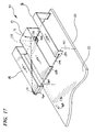
- FIG. 17 is a perspective view of another embodiment of an antenna assembly according to the present invention.
- FIG. 18 is a top plan view of the antenna assembly of FIG. 17.
- FIG. 19 is a side elevational view of the antenna assembly of FIG. 17 .
- FIG. 1 illustrates a wireless communication device 8 , such as a cellular telephone, utilizing an antenna assembly 10 according to the present invention and operating over the cell band frequency range of 824-894 MHz.
- the antenna assembly 10 may be disposed within the communication device 8 at the rear panel 14 and proximate the upper portion of the handset (away from a user's hand), as illustrated in the embodiment of FIG. 1.
- a first embodiment of an antenna assembly 10 includes a driven conductor element 16 and a parasitic conductor element 18 each disposed relative to a ground plane element 20 of the wireless communication device 8 is illustrated in FIGS. 2 and 3.
- the ground plane element 20 may be defined as a portion of the printed wiring board (PWB) 22 of the communication device 8 .
- Driven conductor element 16 includes a conductive surface 24 with first and second leg elements 26 , 28 and may be a singularly formed metallic member.
- Driven conductor element 16 may be a metallic chassis made, for example, of copper or a copper alloy.
- the driven conductor element 16 is approximately “C” shaped when viewed from its side and defines an interior region 30 disposed between the conductive surface 24 and the ground plane element 20 . Components of the communication device 8 may thus be disposed within the interior region 30 to effect a reduction in overall volume of the device.
- the conductive surface 24 is disposed a predetermined distance above the ground plane element 20 and includes a plurality of sections having different widths for effecting optimal operation over the cell band frequency range (824-894 MHz.).
- a first rectangular section 32 is approximately 0.42 inch by 0.61 inch in size for a preferred embodiment.
- a second rectangular section 34 disposed at an upper edge of the first section 32 is approximately 0.1 inch by 0.42 inch in size.
- a third rectangular section 36 disposed at an upper edge of the second section 34 is approximately 0.2 inch by 0.25 inch in size.
- a fourth rectangular section 38 disposed at an upper for a preferred embodiment of the present invention are disclosed in FIGS. 8-9 and Table 1.
- Conductive surface 24 is electrically or operatively connected at an upper edge of the fourth section 38 to a downwardly-directed, perpendicular first leg element 26 which is shorted to the ground plane 20 at foot 40 .
- One or more feet 40 may be practicable to provide for stability of the driven element 16 or routing requirements of the printed wiring board 22 of the communication device. Preferably a single foot 40 is utilized to minimize the contact requirements to the ground plane 20 and otherwise minimize physical interference with other components of the printed wiring board 22 .
- Ground plane element 20 preferably has a minimum length in a direction of polarization ‘DP’ of approximately one-quarter wavelength (for a wavelength within the range of operation). Reference may be made to FIG. 16, wherein an approach to extending the ground plane member 20 of a small hand-held communication device is provided. Driven conductor element 16 may be a single metallic formed element having a thickness within the range of 0.005 to 0.09 inch.
- Second leg element 28 includes a foot 42 which defines one side or plate of a two plate capacitor 46 . Foot 42 is spaced away from the ground plane element 20 by a dielectric element 48 so as to form a capacitor. Dielectric element 48 may have a dielectric constant of between 1-10, and preferably approximately 3.0.
- the parasitic element 18 of antenna assembly includes a ‘C’-shaped element which is spaced away from the driven element 16 .
- Parasitic element 18 includes a conductive portion 50 with first and second leg portions 52 , 54 .
- the conductive leg portions 50 , 52 , 54 of the parasitic element are substantially parallel with and correspond to conductive surfaces and the first and second leg elements 24 , 26 , 28 of the driven element 16 .
- Parasitic element 18 is supported above ground plane 20 by the second leg portion 54 which is capacitively coupled to the ground plane 20 via foot 56 and dielectric member 58 .
- the foot 56 and the dielectric element 58 of the parasitic element 18 form a two plate capacitor 60 .
- the parasitic element 18 is further supported by a first leg portion 52 which is electrically or operatively connected to the ground plane element 20 via foot 40 .
- the parasitic element 18 includes an interior region 68 similar to the interior region 30 of the driven element.
- FIG. 4 illustrates another embodiment of an antenna assembly 10 according to the present invention.
- the driven element 16 and the parasitic element 18 are coupled together via a coupling element 62 .
- the coupling element 62 includes a foot 64 for operatively coupling both the driven element 16 and the parasitic element 18 to the ground plane 20 of the communication device.
- the driven element 16 , parasitic element 18 , and coupling element 62 may be formed from as a single metal part and be fabricated, for example, using high-speed metal stamping processes. In this manner, a compact antenna assembly is provided which is suitable for incorporation within efficient, high volume production of communication devices.
- the antenna element may thus be utilized in conjunction with surface mount device (SMD) production techniques.
- SMD surface mount device
- FIG. 5 illustrates another embodiment of an antenna assembly according to the present invention.
- the antenna of FIG. 5 optimally operates over a pair of frequency ranges, for example, such as cell band (824-894 MHz.) and PCS band (1850-1990 MHz.) ranges. Operation over a higher frequency range is attained by addition of an extension element 66 to the driven conductor element 16 .
- extension element 66 is disposed at a left side edge of the third portion 36 of the driven element 16 .
- Dimensions of the extension element 66 which are sized to effectuate resonance at the higher frequency range, are provided in FIG. 8 and Table 1.
- FIG. 6 illustrates another embodiment of an antenna assembly according to the present invention.
- the driven element 16 , parasitic element 18 , and coupling element 62 are formed as a single unit and operatively connected to the ground plane member 20 at a single ground location via foot 64 .
- FIG. 7 illustrates yet another embodiment of an antenna assembly according to the present invention.
- the driven element 16 , parasitic element 18 , and coupling element 62 are disposed upon a dielectric block or substrate 72 .
- the driven element 16 , parasitic element 18 , and coupling element 62 may be a metal deposition upon the dielectric substrate 72 or formed using other known metal deposition or metal etching processes as those skilled in the relevant arts may appreciate.
- FIGS. 8 and 9, in conjunction with Table 1, disclose dimensions for preferred embodiments of an antenna assembly according to the present invention.
- FIG. 10 illustrates another embodiment of an antenna assembly according to the present invention, in particular a dual band antenna assembly suitable for operation over the cell band (824-894 MHz.) and PCS band (1850-1990 MHz.) frequency ranges.
- This antenna assembly includes low frequency and high frequency driven elements 16 , 17 and low frequency and high frequency parasitic elements 18 , 19 , and for example, all elements being formed as a single stamped metal part.
- a coupling element 62 operatively connects the driven elements 16 , 17 to the parasitic elements 18 , 19 and is formed as a portion of the stamped metal part.
- Coupling element 62 is, in turn, operatively connected to the ground plane member 20 of the communication device 8 at an upper edge thereof.
- Low frequency driven element 16 , low frequency parasitic element 18 , and high frequency parasitic element 19 are each defined by a substantially rectangular planar top surface 74 , 76 , 78 .
- the top surfaces 74 , 76 , 78 are substantially co-planar.
- the high frequency driven element 17 is defined by a substantially rectangular element 80 disposed at a side of the low frequency driven element 16 and downwardly angled toward a foot 82 . Foot 82 is disposed upon a dielectric element 84 to capacitively couple the high frequency driven element 17 to the ground plane member 20 of the communication device.
- Dielectric member 84 may be a ⁇ fraction (1/32) ⁇ inch thickness dielectric substrate having a dielectric constant between 1 and 10, and preferably about 3.0.
- Dielectric member 84 may be a dielectric substrate such as used for printed circuit boards, having a dielectric constant in the range of 1-10, or dielectric member 84 may be a chip capacitor.
- Low frequency driven element 16 and low frequency parasitic element 18 are each operatively coupled at one end to the ground plane member 20 of the communication device via a capacitive coupling 86 , 88 defined between a foot member 90 , 92 and the ground plane 20 .
- a dielectric element 94 may be disposed within each capacitive coupling 86 , 88 .
- high frequency parasitic element 19 includes a free end.
- the antenna assembly of FIG. 10 includes a feed point 12 at which a single conductor from the communication device may be coupled thereto. Operation at alternative frequency ranges may be practicable utilizing the concepts of this embodiment by scaling the relevant dimensions provided herein as those skilled in the arts will appreciate.
- FIG. 11 illustrates another embodiment a multiple band antenna assembly of the present invention.
- Driven element 16 is coupled at feed point 12 to the communication device via a single conductor.
- Driven element 16 is approximately ‘C’ shaped when view in profile and includes a top planar surface including the feed point 12 , a first leg element 26 operatively connected near the upper edge of the ground plane element 20 of the printed wiring board via foot member 40 , and a second leg element 28 capacitively coupled to the ground plane element 20 via foot 92 and capacitor element 94 .
- a parasitic element 18 is disposed relative the driven element 16 and is similarly shaped. Parasitic element 18 is directly or operatively connected at one end near the upper edge of the ground plane element 20 , and capacitively coupled at another end to the ground plane element 20 .
- a perpendicular coupling section 98 is disposed between the driven element 16 and the low frequency parasitic element 18 .
- Coupling section 98 is capacitively coupled to the driven element 16 and the low frequency parasitic element 18 via capacitor elements 96 .
- the dielectric constant of the capacitor elements 96 may range from 1 (air) to approximately 10.
- Antenna assembly of FIG. 11 further includes a high frequency parasitic element 19 directly or operatively connected at one end to the ground plane element 20 of the telecommunication device.
- High frequency parasitic element 19 may be a conductive wire element having a nominal 0.05 inch thickness and including an upper portion substantially aligned with the conductive surface and conductive portion 24 , 50 , respectively, of the driven element 16 and low frequency parasitic element 18 .
- high frequency parasitic element 19 is angled relative to the low frequency parasitic element 18 by an angle “ ⁇ ” of between approximately 5-25 degrees.
- FIG. 12 illustrates yet another embodiment of an antenna assembly 10 according to the present invention.
- the low frequency driven element 16 is directly or operatively connected at a first end to an upper portion 102 of the printed wiring board 22 , and at a lower portion 104 of the printed wiring board 22 through capacitive coupler 86 , and at feed point 12 .
- Low frequency driven element 16 includes a top planar surface 106 including first and second portions 108 , 110 , the first portion 108 defined by a substantially rectangular area and the second portion 110 defined by a relatively smaller rectangular area.
- Feed point 12 is disposed within the second portion 110 of the top planar surface 106 .
- High frequency driven element 80 is directly coupled at an edge of the low frequency driven element 16 (at the second portion 110 ) and is capacitively coupled at the other end to the ground plane 20 of the printed wiring board via foot element 82 and dielectric element 84 .
- High frequency parasitic element 19 which is defined by a substantially rectangular area, is also capacitively coupled to the ground plane member 20 through common foot element 82 and dielectric element 84 .
- the low frequency parasitic element 18 which is disposed on the opposite side of the low frequency driven element 16 , is capacitively coupled at a first end to the ground plane element 20 of the printed wiring board and at the opposite end to a coupling element 62 directly connected to the ground plane element 20 .
- Low frequency parasitic element 18 includes a top planar surface 112 having a plurality of portions defined by varying width dimension. Coupling element 62 electrically connects the low frequency parasitic element 18 to the low frequency driven element 16 .
- FIG. 13 illustrates yet another embodiment of an antenna assembly 10 according to the present invention.
- the driven element 16 is directly or operatively connected at a first end to an upper portion 102 of the printed wiring board 22 , and at a lower portion 104 of the printed wiring board 22 through capacitive coupler 86 .
- the driven element 16 includes a top planar surface including first and second portions 108 , 110 , the first portion 108 defined by a substantially rectangular area and the second portion 110 defined by a relatively smaller rectangular area.
- Driven element 16 further includes a downwardly directed conductive surface 16 a which is coupled at a lower foot surface to a feed point 12 . Operation over a higher frequency range is attained by addition of an extension element 66 to the driven conductor element 16 .
- extension element 66 is disposed at a side edge away from the parasitic element 18 .
- Extension element 66 includes a downwardly directed conductive surface 66 a which is coupled at a lower foot surface to the feed point 12 .
- the feed point 12 is preferably disposed a predetermined distance above the surface of the printed wiring board 22 .
- the foot surface defining the feedpoint 12 is illustrated as a planar surface, though alternatively, the pair of downwardly directed surfaces 16 a, 66 a could be joined without the planar foot surface.
- the parasitic element 18 which is disposed on the side of the driven element 16 opposite the extension element 66 , is capacitively coupled at a first end to the ground plane element 20 of the printed wiring board 22 and at the opposite end to a coupling element 62 directly connected to the ground plane element 20 .
- Parasitic element 18 includes a top planar surface having a plurality of portions defined by varying width dimension. Coupling element 62 electrically connects the parasitic element 18 to the low frequency driven element 16 .
- a dual band antenna includes a driven element 16 for the lower frequency band and a high frequency driven element 17 disposed away therefrom.
- the high frequency and low frequency driven elements 16 , 17 are each defined by substantially planar rectangular portions which are coupled via a conductive spacer portion 114 .
- a feed point 12 is provided between the driven elements 16 , 17 and a signal conductor from the printed wiring board 22 .
- a low frequency parasitic element 18 is disposed further away from the low frequency driven element 16 as indicated.
- FIG. 15 illustrates another preferred embodiment of an antenna assembly according to the present invention wherein the driven elements 16 , 17 and the parasitic element 18 are disposed upon an upper major surface 118 of a dielectric block element 120 .
- the driven elements 16 , 17 and parasitic element 18 may be made as metal depositions upon the dielectric block or otherwise patterned from a plated dielectric stock material.
- Dielectric block element 120 has a dielectric constant of between 1 and 10, and more preferably approximately 3.0.
- the dielectric block 120 is supported a distance away from the printed wiring board 22 of the communication device by conductive spacer elements 124 .
- the spacer elements 124 additionally operatively or directly connect the driven elements 16 , 17 and parasitic elements 19 to the ground plane member 22 at attachment points 134 .
- Low frequency driven element 16 and the parasitic element 18 are each capacitively coupled at respective ends to the ground plane 20 .
- bottom plate elements 126 are disposed upon the opposite major surface 128 of the dielectric substrate 120 and are electrically coupled to the ground plane member 20 via truncated conductive spacer elements 124 .
- a tuner element 130 is disposed at one end of high frequency driven element 17 and may be adjusted relative to the ground plane element 20 to adjust the resonant frequency of the higher frequency antenna.
- FIG. 16 illustrates another aspect of the present invention which provides for an extended ground plane element 140 for use in conjunction with the antenna assemblies disclosed herein.
- the overall length of the ground plane member 20 , 140 (the electrical length) is preferably greater than one-quarter wavelength for a preselected wavelength in the operational frequency band. Applicants have determined that the electrical length of the ground plane 20 , 140 in large part determines the gain of the antenna assembly.
- One limitation of smaller hand held communication devices is that the ground plane 20 , 140 has an electrical length which is less than optimal.
- the ground plane length 20 , 140 may be extended by coupling a conductive panel 144 of the flip panel portion 142 to the main ground plane 20 of the printed wiring board 22 .
- the conductive panel 144 may be a separate conductor element or a conductive layer disposed upon an existing surface of the flip panel portion 142 .
- the coupling device 146 may be selected from among a group of known electrical coupling techniques as appreciated by those skilled in the relevant arts.
- FIGS. 17-19 illustrate another embodiment of an antenna assembly according to the present invention, in particular a dual band antenna assembly suitable for operation over the US cell band (824-894 MHz) and PCS band (1850-1990 MHz) frequency ranges. Operation at alternative frequency ranges may be practicable utilizing the concepts of this embodiment by scaling the relevant dimensions provided herein as those skilled in the arts will appreciate.
- An antenna assembly 10 disclosed in FIGS. 17-19 consists of a voltage-fed, stagger tuned resonator 16 and parasitic resonator element 18 operating at a lower frequency band.
- the resonators 16 , 18 are stagger tuned to promote bandwidth, and are operated in conjunction with a ground plane 20 having a minimum length of 1 ⁇ 4 ⁇ .
- a second shunt fed resonator 17 for one for more higher frequency bands is disposed in operational relationship to the first resonators 16 , 18 .
- this antenna assembly includes low frequency and high frequency resonator elements 16 , 17 and a low frequency parasitic element 18 .
- elements 16 , 17 , 18 may be formed as stamped metal parts. Alternative approaches to manufacturing elements 16 , 17 , 18 would also be appreciated by those skilled in the relevant arts, e.g., plated plastic, wire form, and printed circuit board fabrication.
- Elements 16 , 17 , 18 are each defined by a substantially rectangular planar top surface 150 , 152 , 154 .
- the top surfaces 150 , 152 , 154 are substantially co-planar and disposed a predetermined distance away from the ground plane 20 .
- Elements 16 , 17 , 18 are generally C-shaped and are coupled to the ground plane 20 at one end.
- Elements 16 , 17 , 18 each include a free end 156 , 158 , 160 , respectively, disposed away from the ground connections.
- Elements 16 and 18 may optionally be capacitively coupled to ground plane 20 at respective free ends 156 , 160 by capacitive tuning elements 162 , 164 .
- Optional capacitive tuning elements 162 , 164 may be a chip capacitor, an air dielectric parallel plate capacitor, or other suitable capacitive tuning devices or networks.
- the ground plane 20 forms a portion of the antenna 10 and has a minimum electrical length of 1 ⁇ 4 at the lowest frequency of operation.
- the ground plane 20 may include ground traces of the printed wiring board of a wireless communications device.
- Ground plane 20 of FIGS. 17-19 is illustrated as generally rectangular in shape. Alternative ground plane 20 configurations or shapes may also be utilized to practice an embodiment of the present invention.
- the coupling to ground plane 20 may be made via soldering, or other known electrical coupling techniques.
- High frequency resonator element 17 and the distributed capacitance between element 17 and the ground plane 20 determine the resonant frequency of element 17 .
- Low frequency resonator element 16 and low frequency parasitic element 18 are tuned to the lower frequency band of operation, such as the US cell band, 824-894 MHz, in one preferred embodiment.
- a feed point 12 is defined upon the top surface 152 of the high frequency element 17 .
- High frequency resonator element 17 is shunt fed, with a ground connection at location 166 and a connection to the center conductor 168 of the coax signal line 170 at feed point 12 .
- a conductor 172 is connected to the center conductor 168 of coax signal line 170 .
- Conductor 172 may be an extension of the center conductor 168 of the coax signal line 170 .
- Conductor 172 is also connected to one end of a high impedance line 174 which extends away from feed point 12 and around the free ends 158 , 160 of elements 17 and 18 .
- the high impedance line 174 is connected at its other end to the free end 156 of element 16 .
- the high impedance line 174 is optimally 1 ⁇ 4 ⁇ in electrical length ( ⁇ : approximately at the mid frequency of the band), and serves to transform the 50 ohm input/output impedance to the higher impedance at the free end 156 of element 16 .
- This feed approach in conjunction with stagger tuning of resonator elements 16 , 18 , results in greater bandwidth, gain, and front-to-back ratio as compared to shunt feeding near the low impedance end of element 16 .
- the high impedance line 174 may be a single wire above the ground plane 20 as illustrated in FIG. 17, or alternative may be a microstrip transmission line (not shown).
- an antenna of FIGS. 17-19 exhibits a front to back ratio of 4.5 dB in the lower frequency range, and 6-10 dB in the high frequency range.
- the polarization in both bands is linear, along the major dimension of ground plane 20 .
- a maximum gain is generally in the direction away extending away from the ground plane 20 surface upon which the antenna 10 is disposed.
- FIG. 18 is a top plan view of the antenna assembly of FIG. 17, illustrated in reference to a printed wiring board 22 defining a ground plane 20 and illustrating dimensions of an antenna assembly operational over then particular a dual band antenna assembly suitable for operation over the US cell band (824-894 MHz) and PCS band (1850-1990 MHz) frequency ranges.
- FIG. 19 is a side elevational view of the antenna assembly of FIG. 17, illustrating dimensions of an antenna assembly operational over then particular a dual band antenna assembly suitable for operation over the US cell band (824-894 MHz) and PCS band (1850-1990 MHz) frequency ranges.
- the antenna assemblies provide improved directivity, broadband input impedance, increased signal strength, and increased battery life.
- the antenna of the present invention reduces radio frequency radiation incident to the user's body, and reduces the physical size requirements of directional antenna used in cell phone handsets, PCS devices and the like.
- the disclosed antenna also increases front-to-back ratios, reduces multipath interference, and is easily integrated into the rear panel portion of a cellular transceiver device to minimizes the risk of damage or interference. Additionally, beamwidth and bandwidth enhancement in the direction away from the user is achieved particularly when the antenna assembly is used in conjunction with hand-held wireless communication devices. Beamwidths of 1.5-2 times greater than for a dipole antenna have been recognized.
Abstract
Description
| TABLE 1 | |||
| Dimension | Inch | ||
| i. | 1.600 | ||
| j. | 1.260 | ||
| k. | .925 | ||
| l. | .775 | ||
| m. | .725 | ||
| n. | .400 | ||
| o. | .200 | ||
| p. | .395 | ||
| q. | .200 | ||
| r. | 1.330 | ||
| s. | .100 | ||
| t. | .640 | ||
| u. | .420 | ||
| v. | .360 | ||
| w. | .610 | ||
| x. | .530 | ||
| y. | .950 | ||
| z. | 1.080 | ||
| AA. | 1.200 | ||
Claims (25)
Priority Applications (1)
| Application Number | Priority Date | Filing Date | Title |
|---|---|---|---|
| US09/837,132 US6456249B1 (en) | 1999-08-16 | 2001-04-18 | Single or dual band parasitic antenna assembly |
Applications Claiming Priority (3)
| Application Number | Priority Date | Filing Date | Title |
|---|---|---|---|
| US09/374,782 US6215447B1 (en) | 1998-01-16 | 1999-08-16 | Antenna assembly for communications devices |
| US16351599P | 1999-11-04 | 1999-11-04 | |
| US09/837,132 US6456249B1 (en) | 1999-08-16 | 2001-04-18 | Single or dual band parasitic antenna assembly |
Related Parent Applications (1)
| Application Number | Title | Priority Date | Filing Date |
|---|---|---|---|
| US09/374,782 Continuation-In-Part US6215447B1 (en) | 1998-01-16 | 1999-08-16 | Antenna assembly for communications devices |
Publications (1)
| Publication Number | Publication Date |
|---|---|
| US6456249B1 true US6456249B1 (en) | 2002-09-24 |
Family
ID=26859707
Family Applications (1)
| Application Number | Title | Priority Date | Filing Date |
|---|---|---|---|
| US09/837,132 Expired - Fee Related US6456249B1 (en) | 1999-08-16 | 2001-04-18 | Single or dual band parasitic antenna assembly |
Country Status (1)
| Country | Link |
|---|---|
| US (1) | US6456249B1 (en) |
Cited By (124)
| Publication number | Priority date | Publication date | Assignee | Title |
|---|---|---|---|---|
| US6542123B1 (en) * | 2001-10-24 | 2003-04-01 | Auden Techno Corp. | Hidden wideband antenna |
| US6563467B1 (en) * | 2001-12-28 | 2003-05-13 | Motorola, Inc. | Efficient antenna pattern shaping structure and associated radio circuitry and antenna |
| WO2003041289A1 (en) * | 2001-11-07 | 2003-05-15 | Ems Technologies, Inc. | Linearly-polarized dual-band base-station antenna |
| US6639560B1 (en) * | 2002-04-29 | 2003-10-28 | Centurion Wireless Technologies, Inc. | Single feed tri-band PIFA with parasitic element |
| US20040046694A1 (en) * | 2002-03-14 | 2004-03-11 | Tantivy Communications, Inc. | Mobile communication handset with adaptive antenna array |
| US6707428B2 (en) * | 2001-05-25 | 2004-03-16 | Nokia Corporation | Antenna |
| US6714162B1 (en) * | 2002-10-10 | 2004-03-30 | Centurion Wireless Technologies, Inc. | Narrow width dual/tri ISM band PIFA for wireless applications |
| US20040075613A1 (en) * | 2002-06-21 | 2004-04-22 | Perry Jarmuszewski | Multiple-element antenna with parasitic coupler |
| US20040090375A1 (en) * | 2002-11-13 | 2004-05-13 | Dai Hsin Kuo | Wide-band antenna |
| US20040113845A1 (en) * | 2002-12-16 | 2004-06-17 | Filtronic Lk Oy | Antenna for flat radio device |
| US20040137950A1 (en) * | 2001-03-23 | 2004-07-15 | Thomas Bolin | Built-in, multi band, multi antenna system |
| US20040145526A1 (en) * | 2001-04-16 | 2004-07-29 | Carles Puente Baliarda | Dual-band dual-polarized antenna array |
| EP1447879A1 (en) * | 2003-02-14 | 2004-08-18 | Siemens Aktiengesellschaft | An extension for an antenna ground plate, an antenna ground plate, an antenna, and devices using the same |
| US20040227675A1 (en) * | 2003-02-25 | 2004-11-18 | Nec Corporation | Antenna apparatus having high receiving efficiency |
| US20040227680A1 (en) * | 2003-05-14 | 2004-11-18 | Geyi Wen | Antenna with multiple-band patch and slot structures |
| EP1487051A1 (en) * | 2003-06-12 | 2004-12-15 | Research In Motion Limited | Multiple-element antenna with electromagnetically coupled floating antenna element |
| US20040257292A1 (en) * | 2003-06-20 | 2004-12-23 | Wang Electro-Opto Corporation | Broadband/multi-band circular array antenna |
| US20050017906A1 (en) * | 2003-07-24 | 2005-01-27 | Man Ying Tong | Floating conductor pad for antenna performance stabilization and noise reduction |
| EP1507313A2 (en) * | 2003-08-14 | 2005-02-16 | Nec Corporation | Antenna device for portable terminal |
| US20050043055A1 (en) * | 2003-08-07 | 2005-02-24 | Vance Scott L. | Tunable parasitic resonators |
| US20050078037A1 (en) * | 2003-10-09 | 2005-04-14 | Daniel Leclerc | Internal antenna of small volume |
| US20050093750A1 (en) * | 2003-10-31 | 2005-05-05 | Vance Scott L. | Multi-band planar inverted-F antennas including floating parasitic elements and wireless terminals incorporating the same |
| US20050116863A1 (en) * | 2003-11-27 | 2005-06-02 | Alps Electric Co., Ltd. | Circularly polarized wave antenna device suitable for miniaturization |
| EP1538695A1 (en) * | 2003-12-05 | 2005-06-08 | Alps Electric Co., Ltd. | Miniaturized antenna-coupled module |
| US20050128162A1 (en) * | 2003-12-10 | 2005-06-16 | Matsushita Electric Industrail Co., Ltd. | Antenna |
| US6950071B2 (en) | 2001-04-12 | 2005-09-27 | Research In Motion Limited | Multiple-element antenna |
| US20050287959A1 (en) * | 2004-06-29 | 2005-12-29 | Young-Bong Park | Mobile communication terminal having dual intenna |
| US20060038721A1 (en) * | 2004-08-20 | 2006-02-23 | Mete Ozkar | Planar inverted "F" antenna and method of tuning same |
| US20060055602A1 (en) * | 2003-01-24 | 2006-03-16 | Stefan Huber | Multiband antenna array for mobile radio equipment |
| US20060103584A1 (en) * | 2004-11-18 | 2006-05-18 | Hon Hai Precision Ind. Co., Ltd. | Impedance matching means between antenna and transmission line |
| US20060132363A1 (en) * | 2003-04-04 | 2006-06-22 | Neergaard Per J | Device for shielding electronic units including a transmitting/receiving equipment, and especially for shielding mobile phones |
| US20060211373A1 (en) * | 2005-03-15 | 2006-09-21 | Chia-I Lin | Dual purpose multi-brand monopole antenna |
| US20070057849A1 (en) * | 2005-09-13 | 2007-03-15 | Samsung Electronics Co., Ltd. | Antenna for dual band operation |
| US20070159401A1 (en) * | 2004-02-26 | 2007-07-12 | Baliarda Carles P | Handset with electromagnetic bra |
| US20070188383A1 (en) * | 2004-04-27 | 2007-08-16 | Murata Manufacturing Co., Ltd. | Antenna and portable radio communication apparatus |
| US7265724B1 (en) * | 2006-03-28 | 2007-09-04 | Motorola Inc. | Communications assembly and antenna assembly with a switched tuning line |
| WO2007110250A1 (en) * | 2006-03-27 | 2007-10-04 | Siemens Aktiengesellschaft | Apparatus having a capacitively or inductively loaded planar antenna |
| CN100346531C (en) * | 2003-10-24 | 2007-10-31 | 广达电脑股份有限公司 | Multi-channel antenna |
| US20070257846A1 (en) * | 2004-05-13 | 2007-11-08 | Geyi Wen | Antenna with multiple-band patch and slot structures |
| US20070268187A1 (en) * | 2006-05-19 | 2007-11-22 | Arcadyan Technology Corporation | Inverted-F antenna and manufacturing method thereof |
| US20080036663A1 (en) * | 2005-06-27 | 2008-02-14 | Yukio Sakai | Antenna Device |
| WO2008076977A1 (en) * | 2006-12-18 | 2008-06-26 | Motorola Inc. | Communications assembly and antenna radiator assembly |
| US20080169984A1 (en) * | 2007-01-15 | 2008-07-17 | Naoyuki Takagi | Antenna |
| US20080186238A1 (en) * | 2007-02-01 | 2008-08-07 | Mitsumi Electric Co. Ltd. | Antenna apparatus |
| GB2430081B (en) * | 2004-03-05 | 2008-10-08 | Ibm | Integrated multiband antennas for computing devices |
| US20080303729A1 (en) * | 2005-10-03 | 2008-12-11 | Zlatoljub Milosavljevic | Multiband antenna system and methods |
| US7479928B2 (en) | 2006-03-28 | 2009-01-20 | Motorola, Inc. | Antenna radiator assembly and radio communications assembly |
| US20090046019A1 (en) * | 2004-10-01 | 2009-02-19 | Matsushita Electric Industrial Co., Ltd. | Antenna device and wireless terminal using the antenna device |
| US20090073052A1 (en) * | 2007-09-17 | 2009-03-19 | Hon Hai Precision Ind. Co., Ltd. | Multi-band antenna |
| US20090073055A1 (en) * | 2007-09-14 | 2009-03-19 | Motorola, Inc. | Folded Dipole Multi-Band Antenna |
| US20090080172A1 (en) * | 2007-09-21 | 2009-03-26 | Nokia Corporation | Electromagnetic band gap structures and method for making same |
| WO2009038790A1 (en) * | 2007-09-18 | 2009-03-26 | The Board Of Trustees Of The University Of Illinois | Electrically small antenna devices, systems, apparatus, and methods |
| US20090128442A1 (en) * | 2006-08-24 | 2009-05-21 | Seiken Fujita | Antenna apparatus |
| US20090135066A1 (en) * | 2005-02-08 | 2009-05-28 | Ari Raappana | Internal Monopole Antenna |
| US20090140942A1 (en) * | 2005-10-10 | 2009-06-04 | Jyrki Mikkola | Internal antenna and methods |
| US20090231201A1 (en) * | 2006-05-26 | 2009-09-17 | Petteri Annamaa | Dual Antenna and Methods |
| WO2010123733A1 (en) * | 2009-04-21 | 2010-10-28 | Molex Incorporated | Three dimensional antenna |
| US8009111B2 (en) | 1999-09-20 | 2011-08-30 | Fractus, S.A. | Multilevel antennae |
| WO2011103710A1 (en) * | 2010-02-24 | 2011-09-01 | Laird Technologies Ab | An antenna arrangement for covering a frequency band |
| US20110260939A1 (en) * | 2010-04-21 | 2011-10-27 | Heikki Korva | Distributed multiband antenna and methods |
| WO2011130838A1 (en) * | 2010-04-23 | 2011-10-27 | Psion Inc. | Multiband internal patch antenna for mobile terminals |
| US20110279331A1 (en) * | 2010-05-12 | 2011-11-17 | Qualcomm Incorporated | Apparatus providing thermal management for radio frequency devices |
| US20110312393A1 (en) * | 2010-06-18 | 2011-12-22 | Motorola, Inc. | Antenna system with parasitic element for hearing aid compliant electromagnetic emission |
| WO2012039879A1 (en) * | 2010-09-22 | 2012-03-29 | Apple Inc. | Antenna structures having resonating elements and parasitic elements within slots in conductive elements |
| US20120235871A1 (en) * | 2007-12-26 | 2012-09-20 | Murata Manufacturing Co., Ltd. | Antenna device and radio frequency ic device |
| US20120287009A1 (en) * | 2011-05-10 | 2012-11-15 | Hon Hai Precision Industry Co., Ltd. | Solid antenna |
| US8378892B2 (en) | 2005-03-16 | 2013-02-19 | Pulse Finland Oy | Antenna component and methods |
| US8466756B2 (en) | 2007-04-19 | 2013-06-18 | Pulse Finland Oy | Methods and apparatus for matching an antenna |
| US8473017B2 (en) | 2005-10-14 | 2013-06-25 | Pulse Finland Oy | Adjustable antenna and methods |
| US8531341B2 (en) | 2008-01-04 | 2013-09-10 | Apple Inc. | Antenna isolation for portable electronic devices |
| US8564485B2 (en) | 2005-07-25 | 2013-10-22 | Pulse Finland Oy | Adjustable multiband antenna and methods |
| US8618990B2 (en) | 2011-04-13 | 2013-12-31 | Pulse Finland Oy | Wideband antenna and methods |
| US8629813B2 (en) | 2007-08-30 | 2014-01-14 | Pusle Finland Oy | Adjustable multi-band antenna and methods |
| US8633863B2 (en) * | 2008-03-05 | 2014-01-21 | Ethertronics, Inc. | Modal adaptive antenna using pilot signal in CDMA mobile communication system and related signal receiving method |
| US8648752B2 (en) | 2011-02-11 | 2014-02-11 | Pulse Finland Oy | Chassis-excited antenna apparatus and methods |
| RU2519390C1 (en) * | 2013-01-11 | 2014-06-10 | Корпорация "САМСУНГ ЭЛЕКТРОНИКС Ко., Лтд." | Ultra-wideband compact antenna |
| US8786499B2 (en) * | 2005-10-03 | 2014-07-22 | Pulse Finland Oy | Multiband antenna system and methods |
| US8847833B2 (en) | 2009-12-29 | 2014-09-30 | Pulse Finland Oy | Loop resonator apparatus and methods for enhanced field control |
| US8866689B2 (en) | 2011-07-07 | 2014-10-21 | Pulse Finland Oy | Multi-band antenna and methods for long term evolution wireless system |
| US8965303B2 (en) | 2013-06-21 | 2015-02-24 | Symbol Technologies, Inc. | Quad-band tunable diversity antenna for global applications |
| US8988296B2 (en) | 2012-04-04 | 2015-03-24 | Pulse Finland Oy | Compact polarized antenna and methods |
| US9065179B2 (en) | 2011-09-14 | 2015-06-23 | Tyco Electronics Japan G.K. | Electrical conductive member and electrical conductive member assembly |
| US9123990B2 (en) | 2011-10-07 | 2015-09-01 | Pulse Finland Oy | Multi-feed antenna apparatus and methods |
| US9136601B2 (en) | 2013-05-29 | 2015-09-15 | Motorola Solutions, Inc. | Tunable multiband WAN antenna for global applications |
| US9203139B2 (en) | 2012-05-04 | 2015-12-01 | Apple Inc. | Antenna structures having slot-based parasitic elements |
| US9203137B1 (en) | 2015-03-06 | 2015-12-01 | Apple Inc. | Electronic device with isolated cavity antennas |
| US9203154B2 (en) | 2011-01-25 | 2015-12-01 | Pulse Finland Oy | Multi-resonance antenna, antenna module, radio device and methods |
| US9246210B2 (en) | 2010-02-18 | 2016-01-26 | Pulse Finland Oy | Antenna with cover radiator and methods |
| US9350081B2 (en) | 2014-01-14 | 2016-05-24 | Pulse Finland Oy | Switchable multi-radiator high band antenna apparatus |
| US9350068B2 (en) | 2014-03-10 | 2016-05-24 | Apple Inc. | Electronic device with dual clutch barrel cavity antennas |
| US20160172763A1 (en) * | 2014-12-16 | 2016-06-16 | Laird Technologies, Inc. | Antenna systems with proximity coupled annular rectangular patches |
| US9431717B1 (en) * | 2013-06-25 | 2016-08-30 | Amazon Technologies, Inc. | Wideband dual-arm antenna with parasitic element |
| US9450291B2 (en) | 2011-07-25 | 2016-09-20 | Pulse Finland Oy | Multiband slot loop antenna apparatus and methods |
| US9461371B2 (en) | 2009-11-27 | 2016-10-04 | Pulse Finland Oy | MIMO antenna and methods |
| US9484619B2 (en) | 2011-12-21 | 2016-11-01 | Pulse Finland Oy | Switchable diversity antenna apparatus and methods |
| US9531058B2 (en) | 2011-12-20 | 2016-12-27 | Pulse Finland Oy | Loosely-coupled radio antenna apparatus and methods |
| CN106299597A (en) * | 2012-12-21 | 2017-01-04 | 株式会社村田制作所 | Antenna assembly and electronic equipment |
| US9590308B2 (en) | 2013-12-03 | 2017-03-07 | Pulse Electronics, Inc. | Reduced surface area antenna apparatus and mobile communications devices incorporating the same |
| US9634383B2 (en) | 2013-06-26 | 2017-04-25 | Pulse Finland Oy | Galvanically separated non-interacting antenna sector apparatus and methods |
| US9647338B2 (en) | 2013-03-11 | 2017-05-09 | Pulse Finland Oy | Coupled antenna structure and methods |
| US9673507B2 (en) | 2011-02-11 | 2017-06-06 | Pulse Finland Oy | Chassis-excited antenna apparatus and methods |
| US9680202B2 (en) | 2013-06-05 | 2017-06-13 | Apple Inc. | Electronic devices with antenna windows on opposing housing surfaces |
| US9680212B2 (en) | 2013-11-20 | 2017-06-13 | Pulse Finland Oy | Capacitive grounding methods and apparatus for mobile devices |
| US9722308B2 (en) | 2014-08-28 | 2017-08-01 | Pulse Finland Oy | Low passive intermodulation distributed antenna system for multiple-input multiple-output systems and methods of use |
| CN104662736B (en) * | 2012-09-18 | 2017-08-25 | 艾斯特里克有限公司 | Antenna system for AF panel |
| US9761951B2 (en) | 2009-11-03 | 2017-09-12 | Pulse Finland Oy | Adjustable antenna apparatus and methods |
| US9906260B2 (en) | 2015-07-30 | 2018-02-27 | Pulse Finland Oy | Sensor-based closed loop antenna swapping apparatus and methods |
| US9914184B2 (en) | 2015-10-02 | 2018-03-13 | Te Connectivity Corporation | 3D formed LDS liner and method of manufacturing liner |
| US9948002B2 (en) | 2014-08-26 | 2018-04-17 | Pulse Finland Oy | Antenna apparatus with an integrated proximity sensor and methods |
| US9973228B2 (en) | 2014-08-26 | 2018-05-15 | Pulse Finland Oy | Antenna apparatus with an integrated proximity sensor and methods |
| US9979078B2 (en) | 2012-10-25 | 2018-05-22 | Pulse Finland Oy | Modular cell antenna apparatus and methods |
| USD824885S1 (en) * | 2017-02-25 | 2018-08-07 | Airgain Incorporated | Multiple antennas assembly |
| US10069209B2 (en) | 2012-11-06 | 2018-09-04 | Pulse Finland Oy | Capacitively coupled antenna apparatus and methods |
| US10079428B2 (en) | 2013-03-11 | 2018-09-18 | Pulse Finland Oy | Coupled antenna structure and methods |
| US20180337441A1 (en) * | 2008-03-05 | 2018-11-22 | Ethertronics, Inc. | Antenna And Method For Steering Antenna Beam Direction For Wifi Applications |
| US20190044236A1 (en) * | 2017-08-02 | 2019-02-07 | Pc-Tel, Inc. | One-piece dual-band antenna and ground plane |
| US10268236B2 (en) | 2016-01-27 | 2019-04-23 | Apple Inc. | Electronic devices having ventilation systems with antennas |
| US20190288399A1 (en) * | 2018-03-14 | 2019-09-19 | Panasonic Intellectual Property Management Co., Ltd. | Antenna device |
| US10916846B2 (en) * | 2007-08-20 | 2021-02-09 | Ethertronics, Inc. | Antenna with multiple coupled regions |
| CN112909506A (en) * | 2021-01-16 | 2021-06-04 | 深圳市睿德通讯科技有限公司 | Antenna structure and antenna array |
| US20210376478A1 (en) * | 2020-05-28 | 2021-12-02 | Avx Antenna, Inc. D/B/A Ethertronics, Inc. | Modal Antenna System Including Closed-Loop Parasitic Element |
| US11336025B2 (en) * | 2018-02-21 | 2022-05-17 | Pet Technology Limited | Antenna arrangement and associated method |
| US11942684B2 (en) | 2008-03-05 | 2024-03-26 | KYOCERA AVX Components (San Diego), Inc. | Repeater with multimode antenna |
| US11962102B2 (en) | 2022-05-17 | 2024-04-16 | Neptune Technology Group Inc. | Multi-band stamped sheet metal antenna |
Citations (7)
| Publication number | Priority date | Publication date | Assignee | Title |
|---|---|---|---|---|
| US5420596A (en) * | 1993-11-26 | 1995-05-30 | Motorola, Inc. | Quarter-wave gap-coupled tunable strip antenna |
| US5598169A (en) | 1995-03-24 | 1997-01-28 | Lucent Technologies Inc. | Detector and modulator circuits for passive microwave links |
| US5627550A (en) | 1995-06-15 | 1997-05-06 | Nokia Mobile Phones Ltd. | Wideband double C-patch antenna including gap-coupled parasitic elements |
| US5644319A (en) | 1995-05-31 | 1997-07-01 | Industrial Technology Research Institute | Multi-resonance horizontal-U shaped antenna |
| US5764190A (en) | 1996-07-15 | 1998-06-09 | The Hong Kong University Of Science & Technology | Capacitively loaded PIFA |
| US5966097A (en) * | 1996-06-03 | 1999-10-12 | Mitsubishi Denki Kabushiki Kaisha | Antenna apparatus |
| US6114996A (en) * | 1997-03-31 | 2000-09-05 | Qualcomm Incorporated | Increased bandwidth patch antenna |
-
2001
- 2001-04-18 US US09/837,132 patent/US6456249B1/en not_active Expired - Fee Related
Patent Citations (7)
| Publication number | Priority date | Publication date | Assignee | Title |
|---|---|---|---|---|
| US5420596A (en) * | 1993-11-26 | 1995-05-30 | Motorola, Inc. | Quarter-wave gap-coupled tunable strip antenna |
| US5598169A (en) | 1995-03-24 | 1997-01-28 | Lucent Technologies Inc. | Detector and modulator circuits for passive microwave links |
| US5644319A (en) | 1995-05-31 | 1997-07-01 | Industrial Technology Research Institute | Multi-resonance horizontal-U shaped antenna |
| US5627550A (en) | 1995-06-15 | 1997-05-06 | Nokia Mobile Phones Ltd. | Wideband double C-patch antenna including gap-coupled parasitic elements |
| US5966097A (en) * | 1996-06-03 | 1999-10-12 | Mitsubishi Denki Kabushiki Kaisha | Antenna apparatus |
| US5764190A (en) | 1996-07-15 | 1998-06-09 | The Hong Kong University Of Science & Technology | Capacitively loaded PIFA |
| US6114996A (en) * | 1997-03-31 | 2000-09-05 | Qualcomm Incorporated | Increased bandwidth patch antenna |
Cited By (223)
| Publication number | Priority date | Publication date | Assignee | Title |
|---|---|---|---|---|
| US9761934B2 (en) | 1999-09-20 | 2017-09-12 | Fractus, S.A. | Multilevel antennae |
| US9240632B2 (en) | 1999-09-20 | 2016-01-19 | Fractus, S.A. | Multilevel antennae |
| US8941541B2 (en) | 1999-09-20 | 2015-01-27 | Fractus, S.A. | Multilevel antennae |
| US8330659B2 (en) | 1999-09-20 | 2012-12-11 | Fractus, S.A. | Multilevel antennae |
| US8154463B2 (en) | 1999-09-20 | 2012-04-10 | Fractus, S.A. | Multilevel antennae |
| US8154462B2 (en) | 1999-09-20 | 2012-04-10 | Fractus, S.A. | Multilevel antennae |
| US9054421B2 (en) | 1999-09-20 | 2015-06-09 | Fractus, S.A. | Multilevel antennae |
| US8009111B2 (en) | 1999-09-20 | 2011-08-30 | Fractus, S.A. | Multilevel antennae |
| US9362617B2 (en) | 1999-09-20 | 2016-06-07 | Fractus, S.A. | Multilevel antennae |
| US9000985B2 (en) | 1999-09-20 | 2015-04-07 | Fractus, S.A. | Multilevel antennae |
| US8976069B2 (en) | 1999-09-20 | 2015-03-10 | Fractus, S.A. | Multilevel antennae |
| US10056682B2 (en) | 1999-09-20 | 2018-08-21 | Fractus, S.A. | Multilevel antennae |
| US20040137950A1 (en) * | 2001-03-23 | 2004-07-15 | Thomas Bolin | Built-in, multi band, multi antenna system |
| US6950071B2 (en) | 2001-04-12 | 2005-09-27 | Research In Motion Limited | Multiple-element antenna |
| US20040145526A1 (en) * | 2001-04-16 | 2004-07-29 | Carles Puente Baliarda | Dual-band dual-polarized antenna array |
| US6937206B2 (en) * | 2001-04-16 | 2005-08-30 | Fractus, S.A. | Dual-band dual-polarized antenna array |
| US6707428B2 (en) * | 2001-05-25 | 2004-03-16 | Nokia Corporation | Antenna |
| US6542123B1 (en) * | 2001-10-24 | 2003-04-01 | Auden Techno Corp. | Hidden wideband antenna |
| WO2003041289A1 (en) * | 2001-11-07 | 2003-05-15 | Ems Technologies, Inc. | Linearly-polarized dual-band base-station antenna |
| US6563467B1 (en) * | 2001-12-28 | 2003-05-13 | Motorola, Inc. | Efficient antenna pattern shaping structure and associated radio circuitry and antenna |
| US20070152892A1 (en) * | 2002-03-14 | 2007-07-05 | Ipr Licensing, Inc. | Mobile communication handset with adaptive antenna array |
| US6876331B2 (en) * | 2002-03-14 | 2005-04-05 | Ipr Licensing, Inc. | Mobile communication handset with adaptive antenna array |
| US20050156797A1 (en) * | 2002-03-14 | 2005-07-21 | Ipr Licensing, Inc. | Mobile communication handset with adaptive antenna array |
| US7190313B2 (en) | 2002-03-14 | 2007-03-13 | Ipr Licensing, Inc. | Mobile communication handset with adaptive antenna array |
| US7530180B2 (en) | 2002-03-14 | 2009-05-12 | Ipr Licensing, Inc. | Mobile communication handset with adaptive antenna array |
| US20040046694A1 (en) * | 2002-03-14 | 2004-03-11 | Tantivy Communications, Inc. | Mobile communication handset with adaptive antenna array |
| WO2003094282A3 (en) * | 2002-04-29 | 2004-03-25 | Centurion Wireless Tech Inc | Single feed tri-band pifa with parasitic element |
| WO2003094282A2 (en) * | 2002-04-29 | 2003-11-13 | Centurion Wireless Technologies, Inc. | Single feed tri-band pifa with parasitic element |
| US6639560B1 (en) * | 2002-04-29 | 2003-10-28 | Centurion Wireless Technologies, Inc. | Single feed tri-band PIFA with parasitic element |
| US20050200537A1 (en) * | 2002-06-21 | 2005-09-15 | Research In Motion Limited | Multiple-element antenna with parasitic coupler |
| US7183984B2 (en) | 2002-06-21 | 2007-02-27 | Research In Motion Limited | Multiple-element antenna with parasitic coupler |
| US20040075613A1 (en) * | 2002-06-21 | 2004-04-22 | Perry Jarmuszewski | Multiple-element antenna with parasitic coupler |
| US6891506B2 (en) * | 2002-06-21 | 2005-05-10 | Research In Motion Limited | Multiple-element antenna with parasitic coupler |
| EP1576694A4 (en) * | 2002-10-10 | 2006-01-04 | Centurion Wireless Tech Inc | Narrow width dual/tri ism band pifa for wireless applications |
| US6714162B1 (en) * | 2002-10-10 | 2004-03-30 | Centurion Wireless Technologies, Inc. | Narrow width dual/tri ISM band PIFA for wireless applications |
| WO2004034507A3 (en) * | 2002-10-10 | 2005-08-25 | Centurion Wireless Tech Inc | Narrow width dual/tri ism band pifa for wireless applications |
| US20040070537A1 (en) * | 2002-10-10 | 2004-04-15 | Kadambi Govind R. | Narrow width dual/tri ism band pifa for wireless applications |
| EP1576694A2 (en) * | 2002-10-10 | 2005-09-21 | Centurion Wireless Technologies, Inc. | Narrow width dual/tri ism band pifa for wireless applications |
| US20040090375A1 (en) * | 2002-11-13 | 2004-05-13 | Dai Hsin Kuo | Wide-band antenna |
| US7136019B2 (en) * | 2002-12-16 | 2006-11-14 | Lk Products Oy | Antenna for flat radio device |
| US20040113845A1 (en) * | 2002-12-16 | 2004-06-17 | Filtronic Lk Oy | Antenna for flat radio device |
| US20060055602A1 (en) * | 2003-01-24 | 2006-03-16 | Stefan Huber | Multiband antenna array for mobile radio equipment |
| US7999743B2 (en) * | 2003-01-24 | 2011-08-16 | Hewlett-Packard Development Company, L.P. | Multiband antenna array for mobile radio equipment |
| EP1447879A1 (en) * | 2003-02-14 | 2004-08-18 | Siemens Aktiengesellschaft | An extension for an antenna ground plate, an antenna ground plate, an antenna, and devices using the same |
| US20040227675A1 (en) * | 2003-02-25 | 2004-11-18 | Nec Corporation | Antenna apparatus having high receiving efficiency |
| US7026996B2 (en) * | 2003-02-25 | 2006-04-11 | Nec Corporation | Antenna apparatus having high receiving efficiency |
| US20060132363A1 (en) * | 2003-04-04 | 2006-06-22 | Neergaard Per J | Device for shielding electronic units including a transmitting/receiving equipment, and especially for shielding mobile phones |
| US7365700B2 (en) * | 2003-04-04 | 2008-04-29 | Hannah Zweidorff | Device for shielding electronic units including a transmitting/receiving equipment, and especially for shielding mobile phones |
| US7023387B2 (en) | 2003-05-14 | 2006-04-04 | Research In Motion Limited | Antenna with multiple-band patch and slot structures |
| US7256741B2 (en) | 2003-05-14 | 2007-08-14 | Research In Motion Limited | Antenna with multiple-band patch and slot structures |
| US20040227680A1 (en) * | 2003-05-14 | 2004-11-18 | Geyi Wen | Antenna with multiple-band patch and slot structures |
| US20080246668A1 (en) * | 2003-06-12 | 2008-10-09 | Yihong Qi | Multiple-element antenna with floating antenna element |
| US20070176835A1 (en) * | 2003-06-12 | 2007-08-02 | Yihong Qi | Multiple-element antenna with floating antenna element |
| EP1912279A1 (en) * | 2003-06-12 | 2008-04-16 | Research in Motion Limited | Multiple-element antenna with electromagnetically coupled floating antenna element |
| EP1487051A1 (en) * | 2003-06-12 | 2004-12-15 | Research In Motion Limited | Multiple-element antenna with electromagnetically coupled floating antenna element |
| US7400300B2 (en) | 2003-06-12 | 2008-07-15 | Research In Motion Limited | Multiple-element antenna with floating antenna element |
| US20050001769A1 (en) * | 2003-06-12 | 2005-01-06 | Yihong Qi | Multiple-element antenna with floating antenna element |
| US7148846B2 (en) | 2003-06-12 | 2006-12-12 | Research In Motion Limited | Multiple-element antenna with floating antenna element |
| US8018386B2 (en) | 2003-06-12 | 2011-09-13 | Research In Motion Limited | Multiple-element antenna with floating antenna element |
| US6972729B2 (en) * | 2003-06-20 | 2005-12-06 | Wang Electro-Opto Corporation | Broadband/multi-band circular array antenna |
| US20040257292A1 (en) * | 2003-06-20 | 2004-12-23 | Wang Electro-Opto Corporation | Broadband/multi-band circular array antenna |
| US6980173B2 (en) | 2003-07-24 | 2005-12-27 | Research In Motion Limited | Floating conductor pad for antenna performance stabilization and noise reduction |
| US20050017906A1 (en) * | 2003-07-24 | 2005-01-27 | Man Ying Tong | Floating conductor pad for antenna performance stabilization and noise reduction |
| US20050043055A1 (en) * | 2003-08-07 | 2005-02-24 | Vance Scott L. | Tunable parasitic resonators |
| US7162264B2 (en) * | 2003-08-07 | 2007-01-09 | Sony Ericsson Mobile Communications Ab | Tunable parasitic resonators |
| US7342552B2 (en) * | 2003-08-14 | 2008-03-11 | Nec Corporation | Antenna device for compound portable terminal |
| EP1507313A2 (en) * | 2003-08-14 | 2005-02-16 | Nec Corporation | Antenna device for portable terminal |
| EP1507313A3 (en) * | 2003-08-14 | 2005-12-21 | Nec Corporation | Antenna device for portable terminal |
| US20050078039A1 (en) * | 2003-08-14 | 2005-04-14 | Nec Corporation | Antenna device for compound portable terminal |
| US20050078037A1 (en) * | 2003-10-09 | 2005-04-14 | Daniel Leclerc | Internal antenna of small volume |
| US6903690B2 (en) | 2003-10-09 | 2005-06-07 | Amphenol Socapex | Internal antenna of small volume |
| FR2860927A1 (en) * | 2003-10-09 | 2005-04-15 | Socapex Amphenol | LOW VOLUME INTERNAL ANTENNA |
| WO2005036697A1 (en) * | 2003-10-09 | 2005-04-21 | Amphenol Socapex | Low volume internal antenna |
| CN100346531C (en) * | 2003-10-24 | 2007-10-31 | 广达电脑股份有限公司 | Multi-channel antenna |
| US20050093750A1 (en) * | 2003-10-31 | 2005-05-05 | Vance Scott L. | Multi-band planar inverted-F antennas including floating parasitic elements and wireless terminals incorporating the same |
| US6943733B2 (en) * | 2003-10-31 | 2005-09-13 | Sony Ericsson Mobile Communications, Ab | Multi-band planar inverted-F antennas including floating parasitic elements and wireless terminals incorporating the same |
| US20050116863A1 (en) * | 2003-11-27 | 2005-06-02 | Alps Electric Co., Ltd. | Circularly polarized wave antenna device suitable for miniaturization |
| US6975272B2 (en) * | 2003-11-27 | 2005-12-13 | Alps Electric Co., Ltd. | Circularly polarized wave antenna device suitable for miniaturization |
| US7123197B2 (en) * | 2003-12-05 | 2006-10-17 | Alps Electric Co., Ltd. | Miniaturized antenna-coupled module |
| US20050122268A1 (en) * | 2003-12-05 | 2005-06-09 | Alps Electric Co., Ltd. | Miniaturized antenna-coupled module |
| EP1538695A1 (en) * | 2003-12-05 | 2005-06-08 | Alps Electric Co., Ltd. | Miniaturized antenna-coupled module |
| CN100349323C (en) * | 2003-12-10 | 2007-11-14 | 松下电器产业株式会社 | Antenna |
| US7027000B2 (en) * | 2003-12-10 | 2006-04-11 | Matsushita Electric Industrial Co., Ltd. | Antenna |
| US20050128162A1 (en) * | 2003-12-10 | 2005-06-16 | Matsushita Electric Industrail Co., Ltd. | Antenna |
| US7456792B2 (en) | 2004-02-26 | 2008-11-25 | Fractus, S.A. | Handset with electromagnetic bra |
| US20070159401A1 (en) * | 2004-02-26 | 2007-07-12 | Baliarda Carles P | Handset with electromagnetic bra |
| GB2430081B (en) * | 2004-03-05 | 2008-10-08 | Ibm | Integrated multiband antennas for computing devices |
| US20070188383A1 (en) * | 2004-04-27 | 2007-08-16 | Murata Manufacturing Co., Ltd. | Antenna and portable radio communication apparatus |
| US7369089B2 (en) | 2004-05-13 | 2008-05-06 | Research In Motion Limited | Antenna with multiple-band patch and slot structures |
| US20070257846A1 (en) * | 2004-05-13 | 2007-11-08 | Geyi Wen | Antenna with multiple-band patch and slot structures |
| US20050287959A1 (en) * | 2004-06-29 | 2005-12-29 | Young-Bong Park | Mobile communication terminal having dual intenna |
| US7599725B2 (en) * | 2004-06-29 | 2009-10-06 | Pantech & Curitel Communications, Inc. | Mobile communication terminal having dual intenna |
| US20060038721A1 (en) * | 2004-08-20 | 2006-02-23 | Mete Ozkar | Planar inverted "F" antenna and method of tuning same |
| US7345634B2 (en) * | 2004-08-20 | 2008-03-18 | Kyocera Corporation | Planar inverted “F” antenna and method of tuning same |
| US20090046019A1 (en) * | 2004-10-01 | 2009-02-19 | Matsushita Electric Industrial Co., Ltd. | Antenna device and wireless terminal using the antenna device |
| US7602340B2 (en) * | 2004-10-01 | 2009-10-13 | Panasonic Corporation | Antenna device and wireless terminal using the antenna device |
| US7339545B2 (en) * | 2004-11-18 | 2008-03-04 | Hon Hai Precision Ind. Co., Ltd. | Impedance matching means between antenna and transmission line |
| US20060103584A1 (en) * | 2004-11-18 | 2006-05-18 | Hon Hai Precision Ind. Co., Ltd. | Impedance matching means between antenna and transmission line |
| US20090135066A1 (en) * | 2005-02-08 | 2009-05-28 | Ari Raappana | Internal Monopole Antenna |
| US7433725B2 (en) * | 2005-03-15 | 2008-10-07 | High Tech Computer Corp. | Dual purpose multi-brand monopole antenna |
| US20060211373A1 (en) * | 2005-03-15 | 2006-09-21 | Chia-I Lin | Dual purpose multi-brand monopole antenna |
| US8378892B2 (en) | 2005-03-16 | 2013-02-19 | Pulse Finland Oy | Antenna component and methods |
| US20080036663A1 (en) * | 2005-06-27 | 2008-02-14 | Yukio Sakai | Antenna Device |
| US8564485B2 (en) | 2005-07-25 | 2013-10-22 | Pulse Finland Oy | Adjustable multiband antenna and methods |
| US20070057849A1 (en) * | 2005-09-13 | 2007-03-15 | Samsung Electronics Co., Ltd. | Antenna for dual band operation |
| US7889143B2 (en) | 2005-10-03 | 2011-02-15 | Pulse Finland Oy | Multiband antenna system and methods |
| US20100149057A9 (en) * | 2005-10-03 | 2010-06-17 | Zlatoljub Milosavljevic | Multiband antenna system and methods |
| US8786499B2 (en) * | 2005-10-03 | 2014-07-22 | Pulse Finland Oy | Multiband antenna system and methods |
| US20080303729A1 (en) * | 2005-10-03 | 2008-12-11 | Zlatoljub Milosavljevic | Multiband antenna system and methods |
| US7903035B2 (en) | 2005-10-10 | 2011-03-08 | Pulse Finland Oy | Internal antenna and methods |
| US20090140942A1 (en) * | 2005-10-10 | 2009-06-04 | Jyrki Mikkola | Internal antenna and methods |
| US8473017B2 (en) | 2005-10-14 | 2013-06-25 | Pulse Finland Oy | Adjustable antenna and methods |
| WO2007110250A1 (en) * | 2006-03-27 | 2007-10-04 | Siemens Aktiengesellschaft | Apparatus having a capacitively or inductively loaded planar antenna |
| US7479928B2 (en) | 2006-03-28 | 2009-01-20 | Motorola, Inc. | Antenna radiator assembly and radio communications assembly |
| US7265724B1 (en) * | 2006-03-28 | 2007-09-04 | Motorola Inc. | Communications assembly and antenna assembly with a switched tuning line |
| US20070268187A1 (en) * | 2006-05-19 | 2007-11-22 | Arcadyan Technology Corporation | Inverted-F antenna and manufacturing method thereof |
| US8098202B2 (en) | 2006-05-26 | 2012-01-17 | Pulse Finland Oy | Dual antenna and methods |
| US20090231201A1 (en) * | 2006-05-26 | 2009-09-17 | Petteri Annamaa | Dual Antenna and Methods |
| US20090128442A1 (en) * | 2006-08-24 | 2009-05-21 | Seiken Fujita | Antenna apparatus |
| US8193989B2 (en) * | 2006-08-24 | 2012-06-05 | Hitachi Kokusai Electric Inc. | Antenna apparatus |
| WO2008076977A1 (en) * | 2006-12-18 | 2008-06-26 | Motorola Inc. | Communications assembly and antenna radiator assembly |
| US7528783B2 (en) * | 2007-01-15 | 2009-05-05 | Panasonic Corporation | Antenna |
| US20080169984A1 (en) * | 2007-01-15 | 2008-07-17 | Naoyuki Takagi | Antenna |
| US20080186238A1 (en) * | 2007-02-01 | 2008-08-07 | Mitsumi Electric Co. Ltd. | Antenna apparatus |
| EP1956681A1 (en) * | 2007-02-01 | 2008-08-13 | Mitsumi Electric Co., Ltd. | Antenna apparatus |
| US7649498B2 (en) | 2007-02-01 | 2010-01-19 | Mitsumi Electric Co., Ltd. | Antenna apparatus |
| US8466756B2 (en) | 2007-04-19 | 2013-06-18 | Pulse Finland Oy | Methods and apparatus for matching an antenna |
| US11764472B2 (en) | 2007-08-20 | 2023-09-19 | KYOCERA AVX Components (San Diego), Inc. | Antenna with multiple coupled regions |
| US10916846B2 (en) * | 2007-08-20 | 2021-02-09 | Ethertronics, Inc. | Antenna with multiple coupled regions |
| US8629813B2 (en) | 2007-08-30 | 2014-01-14 | Pusle Finland Oy | Adjustable multi-band antenna and methods |
| US7724196B2 (en) * | 2007-09-14 | 2010-05-25 | Motorola, Inc. | Folded dipole multi-band antenna |
| US20090073055A1 (en) * | 2007-09-14 | 2009-03-19 | Motorola, Inc. | Folded Dipole Multi-Band Antenna |
| US8120535B2 (en) * | 2007-09-17 | 2012-02-21 | Hon Hai Precision Ind. Co., Ltd | Multi-band antenna with improved connecting portion |
| US20090073052A1 (en) * | 2007-09-17 | 2009-03-19 | Hon Hai Precision Ind. Co., Ltd. | Multi-band antenna |
| US20090146893A1 (en) * | 2007-09-18 | 2009-06-11 | Mayes Paul E | Electrically small antenna devices, systems, apparatus, and methods |
| US8026860B2 (en) | 2007-09-18 | 2011-09-27 | The Board Of Trustees Of The University Of Illinois | Electrically small antenna devices, systems, apparatus, and methods |
| WO2009038790A1 (en) * | 2007-09-18 | 2009-03-26 | The Board Of Trustees Of The University Of Illinois | Electrically small antenna devices, systems, apparatus, and methods |
| US8159832B2 (en) * | 2007-09-21 | 2012-04-17 | Nokia Corporation | Electromagnetic band gap structures and method for making same |
| US20090080172A1 (en) * | 2007-09-21 | 2009-03-26 | Nokia Corporation | Electromagnetic band gap structures and method for making same |
| US8915448B2 (en) * | 2007-12-26 | 2014-12-23 | Murata Manufacturing Co., Ltd. | Antenna device and radio frequency IC device |
| US20120235871A1 (en) * | 2007-12-26 | 2012-09-20 | Murata Manufacturing Co., Ltd. | Antenna device and radio frequency ic device |
| US8531341B2 (en) | 2008-01-04 | 2013-09-10 | Apple Inc. | Antenna isolation for portable electronic devices |
| US8633863B2 (en) * | 2008-03-05 | 2014-01-21 | Ethertronics, Inc. | Modal adaptive antenna using pilot signal in CDMA mobile communication system and related signal receiving method |
| US11245179B2 (en) | 2008-03-05 | 2022-02-08 | Ethertronics, Inc. | Antenna and method for steering antenna beam direction for WiFi applications |
| US10547102B2 (en) * | 2008-03-05 | 2020-01-28 | Ethertronics, Inc. | Antenna and method for steering antenna beam direction for WiFi applications |
| US11942684B2 (en) | 2008-03-05 | 2024-03-26 | KYOCERA AVX Components (San Diego), Inc. | Repeater with multimode antenna |
| US20180337441A1 (en) * | 2008-03-05 | 2018-11-22 | Ethertronics, Inc. | Antenna And Method For Steering Antenna Beam Direction For Wifi Applications |
| WO2010123733A1 (en) * | 2009-04-21 | 2010-10-28 | Molex Incorporated | Three dimensional antenna |
| US9761951B2 (en) | 2009-11-03 | 2017-09-12 | Pulse Finland Oy | Adjustable antenna apparatus and methods |
| US9461371B2 (en) | 2009-11-27 | 2016-10-04 | Pulse Finland Oy | MIMO antenna and methods |
| US8847833B2 (en) | 2009-12-29 | 2014-09-30 | Pulse Finland Oy | Loop resonator apparatus and methods for enhanced field control |
| US9246210B2 (en) | 2010-02-18 | 2016-01-26 | Pulse Finland Oy | Antenna with cover radiator and methods |
| WO2011103710A1 (en) * | 2010-02-24 | 2011-09-01 | Laird Technologies Ab | An antenna arrangement for covering a frequency band |
| US9406998B2 (en) * | 2010-04-21 | 2016-08-02 | Pulse Finland Oy | Distributed multiband antenna and methods |
| US20110260939A1 (en) * | 2010-04-21 | 2011-10-27 | Heikki Korva | Distributed multiband antenna and methods |
| WO2011130838A1 (en) * | 2010-04-23 | 2011-10-27 | Psion Inc. | Multiband internal patch antenna for mobile terminals |
| JP2015181257A (en) * | 2010-05-12 | 2015-10-15 | クゥアルコム・インコーポレイテッドQualcomm Incorporated | Apparatus for providing heat management for wireless frequency device |
| US20110279331A1 (en) * | 2010-05-12 | 2011-11-17 | Qualcomm Incorporated | Apparatus providing thermal management for radio frequency devices |
| CN102884674B (en) * | 2010-05-12 | 2015-08-05 | 高通股份有限公司 | For radio-frequency apparatus provides the device of heat management |
| CN102884674A (en) * | 2010-05-12 | 2013-01-16 | 高通股份有限公司 | Apparatus providing thermal management for radio frequency devices |
| US8570224B2 (en) * | 2010-05-12 | 2013-10-29 | Qualcomm Incorporated | Apparatus providing thermal management for radio frequency devices |
| US20110312393A1 (en) * | 2010-06-18 | 2011-12-22 | Motorola, Inc. | Antenna system with parasitic element for hearing aid compliant electromagnetic emission |
| US8605922B2 (en) * | 2010-06-18 | 2013-12-10 | Motorola Mobility Llc | Antenna system with parasitic element for hearing aid compliant electromagnetic emission |
| US8483415B2 (en) * | 2010-06-18 | 2013-07-09 | Motorola Mobility Llc | Antenna system with parasitic element for hearing aid compliant electromagnetic emission |
| US20130273963A1 (en) * | 2010-06-18 | 2013-10-17 | Motorola Mobiltiy LLC | Antenna system with parasitic element for hearing aid compliant electromagnetic emission |
| US9531071B2 (en) | 2010-09-22 | 2016-12-27 | Apple Inc. | Antenna structures having resonating elements and parasitic elements within slots in conductive elements |
| WO2012039879A1 (en) * | 2010-09-22 | 2012-03-29 | Apple Inc. | Antenna structures having resonating elements and parasitic elements within slots in conductive elements |
| US9236648B2 (en) | 2010-09-22 | 2016-01-12 | Apple Inc. | Antenna structures having resonating elements and parasitic elements within slots in conductive elements |
| US9203154B2 (en) | 2011-01-25 | 2015-12-01 | Pulse Finland Oy | Multi-resonance antenna, antenna module, radio device and methods |
| US9673507B2 (en) | 2011-02-11 | 2017-06-06 | Pulse Finland Oy | Chassis-excited antenna apparatus and methods |
| US8648752B2 (en) | 2011-02-11 | 2014-02-11 | Pulse Finland Oy | Chassis-excited antenna apparatus and methods |
| US9917346B2 (en) | 2011-02-11 | 2018-03-13 | Pulse Finland Oy | Chassis-excited antenna apparatus and methods |
| US8618990B2 (en) | 2011-04-13 | 2013-12-31 | Pulse Finland Oy | Wideband antenna and methods |
| US20120287009A1 (en) * | 2011-05-10 | 2012-11-15 | Hon Hai Precision Industry Co., Ltd. | Solid antenna |
| US8866689B2 (en) | 2011-07-07 | 2014-10-21 | Pulse Finland Oy | Multi-band antenna and methods for long term evolution wireless system |
| US9450291B2 (en) | 2011-07-25 | 2016-09-20 | Pulse Finland Oy | Multiband slot loop antenna apparatus and methods |
| US9065179B2 (en) | 2011-09-14 | 2015-06-23 | Tyco Electronics Japan G.K. | Electrical conductive member and electrical conductive member assembly |
| US9123990B2 (en) | 2011-10-07 | 2015-09-01 | Pulse Finland Oy | Multi-feed antenna apparatus and methods |
| US9531058B2 (en) | 2011-12-20 | 2016-12-27 | Pulse Finland Oy | Loosely-coupled radio antenna apparatus and methods |
| US9484619B2 (en) | 2011-12-21 | 2016-11-01 | Pulse Finland Oy | Switchable diversity antenna apparatus and methods |
| US9509054B2 (en) | 2012-04-04 | 2016-11-29 | Pulse Finland Oy | Compact polarized antenna and methods |
| US8988296B2 (en) | 2012-04-04 | 2015-03-24 | Pulse Finland Oy | Compact polarized antenna and methods |
| US9203139B2 (en) | 2012-05-04 | 2015-12-01 | Apple Inc. | Antenna structures having slot-based parasitic elements |
| CN104662736B (en) * | 2012-09-18 | 2017-08-25 | 艾斯特里克有限公司 | Antenna system for AF panel |
| US9979078B2 (en) | 2012-10-25 | 2018-05-22 | Pulse Finland Oy | Modular cell antenna apparatus and methods |
| US10069209B2 (en) | 2012-11-06 | 2018-09-04 | Pulse Finland Oy | Capacitively coupled antenna apparatus and methods |
| CN106299597A (en) * | 2012-12-21 | 2017-01-04 | 株式会社村田制作所 | Antenna assembly and electronic equipment |
| CN106299597B (en) * | 2012-12-21 | 2019-05-17 | 株式会社村田制作所 | Antenna assembly and electronic equipment |
| RU2519390C1 (en) * | 2013-01-11 | 2014-06-10 | Корпорация "САМСУНГ ЭЛЕКТРОНИКС Ко., Лтд." | Ultra-wideband compact antenna |
| US9647338B2 (en) | 2013-03-11 | 2017-05-09 | Pulse Finland Oy | Coupled antenna structure and methods |
| US10079428B2 (en) | 2013-03-11 | 2018-09-18 | Pulse Finland Oy | Coupled antenna structure and methods |
| US9136601B2 (en) | 2013-05-29 | 2015-09-15 | Motorola Solutions, Inc. | Tunable multiband WAN antenna for global applications |
| US9680202B2 (en) | 2013-06-05 | 2017-06-13 | Apple Inc. | Electronic devices with antenna windows on opposing housing surfaces |
| US8965303B2 (en) | 2013-06-21 | 2015-02-24 | Symbol Technologies, Inc. | Quad-band tunable diversity antenna for global applications |
| US9431717B1 (en) * | 2013-06-25 | 2016-08-30 | Amazon Technologies, Inc. | Wideband dual-arm antenna with parasitic element |
| US9634383B2 (en) | 2013-06-26 | 2017-04-25 | Pulse Finland Oy | Galvanically separated non-interacting antenna sector apparatus and methods |
| US9680212B2 (en) | 2013-11-20 | 2017-06-13 | Pulse Finland Oy | Capacitive grounding methods and apparatus for mobile devices |
| US9590308B2 (en) | 2013-12-03 | 2017-03-07 | Pulse Electronics, Inc. | Reduced surface area antenna apparatus and mobile communications devices incorporating the same |
| US9350081B2 (en) | 2014-01-14 | 2016-05-24 | Pulse Finland Oy | Switchable multi-radiator high band antenna apparatus |
| US9350068B2 (en) | 2014-03-10 | 2016-05-24 | Apple Inc. | Electronic device with dual clutch barrel cavity antennas |
| US9450289B2 (en) | 2014-03-10 | 2016-09-20 | Apple Inc. | Electronic device with dual clutch barrel cavity antennas |
| US9559406B2 (en) | 2014-03-10 | 2017-01-31 | Apple Inc. | Electronic device with dual clutch barrel cavity antennas |
| US9973228B2 (en) | 2014-08-26 | 2018-05-15 | Pulse Finland Oy | Antenna apparatus with an integrated proximity sensor and methods |
| US9948002B2 (en) | 2014-08-26 | 2018-04-17 | Pulse Finland Oy | Antenna apparatus with an integrated proximity sensor and methods |
| US9722308B2 (en) | 2014-08-28 | 2017-08-01 | Pulse Finland Oy | Low passive intermodulation distributed antenna system for multiple-input multiple-output systems and methods of use |
| US20160172763A1 (en) * | 2014-12-16 | 2016-06-16 | Laird Technologies, Inc. | Antenna systems with proximity coupled annular rectangular patches |
| US9748654B2 (en) * | 2014-12-16 | 2017-08-29 | Laird Technologies, Inc. | Antenna systems with proximity coupled annular rectangular patches |
| US9203137B1 (en) | 2015-03-06 | 2015-12-01 | Apple Inc. | Electronic device with isolated cavity antennas |
| US9653777B2 (en) | 2015-03-06 | 2017-05-16 | Apple Inc. | Electronic device with isolated cavity antennas |
| US9397387B1 (en) | 2015-03-06 | 2016-07-19 | Apple Inc. | Electronic device with isolated cavity antennas |
| US9906260B2 (en) | 2015-07-30 | 2018-02-27 | Pulse Finland Oy | Sensor-based closed loop antenna swapping apparatus and methods |
| US9914184B2 (en) | 2015-10-02 | 2018-03-13 | Te Connectivity Corporation | 3D formed LDS liner and method of manufacturing liner |
| US10268236B2 (en) | 2016-01-27 | 2019-04-23 | Apple Inc. | Electronic devices having ventilation systems with antennas |
| USD824885S1 (en) * | 2017-02-25 | 2018-08-07 | Airgain Incorporated | Multiple antennas assembly |
| US20190044236A1 (en) * | 2017-08-02 | 2019-02-07 | Pc-Tel, Inc. | One-piece dual-band antenna and ground plane |
| US11336025B2 (en) * | 2018-02-21 | 2022-05-17 | Pet Technology Limited | Antenna arrangement and associated method |
| US20190288399A1 (en) * | 2018-03-14 | 2019-09-19 | Panasonic Intellectual Property Management Co., Ltd. | Antenna device |
| US10886621B2 (en) * | 2018-03-14 | 2021-01-05 | Panasonic Intellectual Property Management Co., Ltd. | Antenna device |
| US20210376478A1 (en) * | 2020-05-28 | 2021-12-02 | Avx Antenna, Inc. D/B/A Ethertronics, Inc. | Modal Antenna System Including Closed-Loop Parasitic Element |
| US11735826B2 (en) * | 2020-05-28 | 2023-08-22 | KYOCERA AVX Components (San Diego), Inc. | Modal antenna system including closed-loop parasitic element |
| CN112909506A (en) * | 2021-01-16 | 2021-06-04 | 深圳市睿德通讯科技有限公司 | Antenna structure and antenna array |
| US11183752B2 (en) * | 2021-01-16 | 2021-11-23 | Etheta Communication Technology(Shenzhen)Co.,Ltd | Antenna structure and antenna array |
| US11962102B2 (en) | 2022-05-17 | 2024-04-16 | Neptune Technology Group Inc. | Multi-band stamped sheet metal antenna |
Similar Documents
| Publication | Publication Date | Title |
|---|---|---|
| US6456249B1 (en) | Single or dual band parasitic antenna assembly | |
| US6429818B1 (en) | Single or dual band parasitic antenna assembly | |
| WO2001033665A1 (en) | Single or dual band parasitic antenna assembly | |
| US6215447B1 (en) | Antenna assembly for communications devices | |
| US6404394B1 (en) | Dual polarization slot antenna assembly | |
| US6407710B2 (en) | Compact dual frequency antenna with multiple polarization | |
| US6268831B1 (en) | Inverted-f antennas with multiple planar radiating elements and wireless communicators incorporating same | |
| US7564413B2 (en) | Multi-band antenna and mobile communication terminal having the same | |
| US6204826B1 (en) | Flat dual frequency band antennas for wireless communicators | |
| US7319431B2 (en) | Surface mount antenna apparatus having triple land structure | |
| EP1569300B1 (en) | Wireless device having antenna | |
| US8618990B2 (en) | Wideband antenna and methods | |
| US6326927B1 (en) | Capacitively-tuned broadband antenna structure | |
| US20020075187A1 (en) | Low SAR broadband antenna assembly | |
| US6229487B1 (en) | Inverted-F antennas having non-linear conductive elements and wireless communicators incorporating the same | |
| US20100060528A1 (en) | Dual-frequency antenna | |
| EP0851533A1 (en) | An inverted-E antenna | |
| EP1629569B1 (en) | Internal antenna with slots | |
| US6563466B2 (en) | Multi-frequency band inverted-F antennas with coupled branches and wireless communicators incorporating same | |
| US20020177416A1 (en) | Radio communications device | |
| US20060290575A1 (en) | Antenna integrated into a housing | |
| US6646619B2 (en) | Broadband antenna assembly of matching circuitry and ground plane conductive radiating element | |
| US6515627B2 (en) | Multiple band antenna having isolated feeds | |
| US6697023B1 (en) | Built-in multi-band mobile phone antenna with meandering conductive portions | |
| KR100972846B1 (en) | Multi bandwidth antenna for mobile phone |
Legal Events
| Date | Code | Title | Description |
|---|---|---|---|
| AS | Assignment |
Owner name: RANGESTAR WIRELESS, INC., CALIFORNIA Free format text: ASSIGNMENT OF ASSIGNORS INTEREST;ASSIGNOR:NEWMAN, BEN;REEL/FRAME:011732/0495 Effective date: 20010417 Owner name: RANGESTAR WIRELESS, INC., CALIFORNIA Free format text: ASSIGNMENT OF ASSIGNORS INTEREST;ASSIGNOR:JOHNSON, GREG;REEL/FRAME:011732/0503 Effective date: 20010417 |
|
| FPAY | Fee payment |
Year of fee payment: 4 |
|
| FPAY | Fee payment |
Year of fee payment: 8 |
|
| REMI | Maintenance fee reminder mailed | ||
| LAPS | Lapse for failure to pay maintenance fees | ||
| STCH | Information on status: patent discontinuation |
Free format text: PATENT EXPIRED DUE TO NONPAYMENT OF MAINTENANCE FEES UNDER 37 CFR 1.362 |
|
| FP | Lapsed due to failure to pay maintenance fee |
Effective date: 20140924 |