US6456279B1 - Liquid crystal display device with a touch panel - Google Patents
Liquid crystal display device with a touch panel Download PDFInfo
- Publication number
- US6456279B1 US6456279B1 US09/352,359 US35235999A US6456279B1 US 6456279 B1 US6456279 B1 US 6456279B1 US 35235999 A US35235999 A US 35235999A US 6456279 B1 US6456279 B1 US 6456279B1
- Authority
- US
- United States
- Prior art keywords
- substrate
- liquid crystal
- crystal display
- transparent
- display device
- Prior art date
- Legal status (The legal status is an assumption and is not a legal conclusion. Google has not performed a legal analysis and makes no representation as to the accuracy of the status listed.)
- Expired - Lifetime
Links
Images


Classifications
-
- G—PHYSICS
- G06—COMPUTING; CALCULATING OR COUNTING
- G06F—ELECTRIC DIGITAL DATA PROCESSING
- G06F3/00—Input arrangements for transferring data to be processed into a form capable of being handled by the computer; Output arrangements for transferring data from processing unit to output unit, e.g. interface arrangements
- G06F3/01—Input arrangements or combined input and output arrangements for interaction between user and computer
- G06F3/03—Arrangements for converting the position or the displacement of a member into a coded form
- G06F3/041—Digitisers, e.g. for touch screens or touch pads, characterised by the transducing means
-
- G—PHYSICS
- G02—OPTICS
- G02F—OPTICAL DEVICES OR ARRANGEMENTS FOR THE CONTROL OF LIGHT BY MODIFICATION OF THE OPTICAL PROPERTIES OF THE MEDIA OF THE ELEMENTS INVOLVED THEREIN; NON-LINEAR OPTICS; FREQUENCY-CHANGING OF LIGHT; OPTICAL LOGIC ELEMENTS; OPTICAL ANALOGUE/DIGITAL CONVERTERS
- G02F1/00—Devices or arrangements for the control of the intensity, colour, phase, polarisation or direction of light arriving from an independent light source, e.g. switching, gating or modulating; Non-linear optics
- G02F1/01—Devices or arrangements for the control of the intensity, colour, phase, polarisation or direction of light arriving from an independent light source, e.g. switching, gating or modulating; Non-linear optics for the control of the intensity, phase, polarisation or colour
- G02F1/13—Devices or arrangements for the control of the intensity, colour, phase, polarisation or direction of light arriving from an independent light source, e.g. switching, gating or modulating; Non-linear optics for the control of the intensity, phase, polarisation or colour based on liquid crystals, e.g. single liquid crystal display cells
- G02F1/133—Constructional arrangements; Operation of liquid crystal cells; Circuit arrangements
- G02F1/1333—Constructional arrangements; Manufacturing methods
- G02F1/13338—Input devices, e.g. touch panels
-
- G—PHYSICS
- G02—OPTICS
- G02F—OPTICAL DEVICES OR ARRANGEMENTS FOR THE CONTROL OF LIGHT BY MODIFICATION OF THE OPTICAL PROPERTIES OF THE MEDIA OF THE ELEMENTS INVOLVED THEREIN; NON-LINEAR OPTICS; FREQUENCY-CHANGING OF LIGHT; OPTICAL LOGIC ELEMENTS; OPTICAL ANALOGUE/DIGITAL CONVERTERS
- G02F1/00—Devices or arrangements for the control of the intensity, colour, phase, polarisation or direction of light arriving from an independent light source, e.g. switching, gating or modulating; Non-linear optics
- G02F1/01—Devices or arrangements for the control of the intensity, colour, phase, polarisation or direction of light arriving from an independent light source, e.g. switching, gating or modulating; Non-linear optics for the control of the intensity, phase, polarisation or colour
- G02F1/13—Devices or arrangements for the control of the intensity, colour, phase, polarisation or direction of light arriving from an independent light source, e.g. switching, gating or modulating; Non-linear optics for the control of the intensity, phase, polarisation or colour based on liquid crystals, e.g. single liquid crystal display cells
- G02F1/133—Constructional arrangements; Operation of liquid crystal cells; Circuit arrangements
- G02F1/1333—Constructional arrangements; Manufacturing methods
- G02F1/1335—Structural association of cells with optical devices, e.g. polarisers or reflectors
-
- G—PHYSICS
- G06—COMPUTING; CALCULATING OR COUNTING
- G06F—ELECTRIC DIGITAL DATA PROCESSING
- G06F3/00—Input arrangements for transferring data to be processed into a form capable of being handled by the computer; Output arrangements for transferring data from processing unit to output unit, e.g. interface arrangements
- G06F3/01—Input arrangements or combined input and output arrangements for interaction between user and computer
- G06F3/03—Arrangements for converting the position or the displacement of a member into a coded form
- G06F3/041—Digitisers, e.g. for touch screens or touch pads, characterised by the transducing means
- G06F3/0412—Digitisers structurally integrated in a display
-
- G—PHYSICS
- G06—COMPUTING; CALCULATING OR COUNTING
- G06F—ELECTRIC DIGITAL DATA PROCESSING
- G06F3/00—Input arrangements for transferring data to be processed into a form capable of being handled by the computer; Output arrangements for transferring data from processing unit to output unit, e.g. interface arrangements
- G06F3/01—Input arrangements or combined input and output arrangements for interaction between user and computer
- G06F3/03—Arrangements for converting the position or the displacement of a member into a coded form
- G06F3/041—Digitisers, e.g. for touch screens or touch pads, characterised by the transducing means
- G06F3/045—Digitisers, e.g. for touch screens or touch pads, characterised by the transducing means using resistive elements, e.g. a single continuous surface or two parallel surfaces put in contact
-
- G—PHYSICS
- G06—COMPUTING; CALCULATING OR COUNTING
- G06F—ELECTRIC DIGITAL DATA PROCESSING
- G06F3/00—Input arrangements for transferring data to be processed into a form capable of being handled by the computer; Output arrangements for transferring data from processing unit to output unit, e.g. interface arrangements
- G06F3/01—Input arrangements or combined input and output arrangements for interaction between user and computer
- G06F3/048—Interaction techniques based on graphical user interfaces [GUI]
- G06F3/0487—Interaction techniques based on graphical user interfaces [GUI] using specific features provided by the input device, e.g. functions controlled by the rotation of a mouse with dual sensing arrangements, or of the nature of the input device, e.g. tap gestures based on pressure sensed by a digitiser
- G06F3/0488—Interaction techniques based on graphical user interfaces [GUI] using specific features provided by the input device, e.g. functions controlled by the rotation of a mouse with dual sensing arrangements, or of the nature of the input device, e.g. tap gestures based on pressure sensed by a digitiser using a touch-screen or digitiser, e.g. input of commands through traced gestures
-
- G—PHYSICS
- G02—OPTICS
- G02F—OPTICAL DEVICES OR ARRANGEMENTS FOR THE CONTROL OF LIGHT BY MODIFICATION OF THE OPTICAL PROPERTIES OF THE MEDIA OF THE ELEMENTS INVOLVED THEREIN; NON-LINEAR OPTICS; FREQUENCY-CHANGING OF LIGHT; OPTICAL LOGIC ELEMENTS; OPTICAL ANALOGUE/DIGITAL CONVERTERS
- G02F1/00—Devices or arrangements for the control of the intensity, colour, phase, polarisation or direction of light arriving from an independent light source, e.g. switching, gating or modulating; Non-linear optics
- G02F1/01—Devices or arrangements for the control of the intensity, colour, phase, polarisation or direction of light arriving from an independent light source, e.g. switching, gating or modulating; Non-linear optics for the control of the intensity, phase, polarisation or colour
- G02F1/13—Devices or arrangements for the control of the intensity, colour, phase, polarisation or direction of light arriving from an independent light source, e.g. switching, gating or modulating; Non-linear optics for the control of the intensity, phase, polarisation or colour based on liquid crystals, e.g. single liquid crystal display cells
- G02F1/133—Constructional arrangements; Operation of liquid crystal cells; Circuit arrangements
- G02F1/1333—Constructional arrangements; Manufacturing methods
- G02F1/1335—Structural association of cells with optical devices, e.g. polarisers or reflectors
- G02F1/1336—Illuminating devices
- G02F1/133616—Front illuminating devices
Definitions
- the present invention relates to a liquid crystal display device and, more particularly, to a liquid crystal display device in which an illumination light source and a touch panel are stacked on a reflection type of liquid crystal panel which modulates light incident from its display-surface side and allows the modulated light to exit toward the display-surface side.
- liquid crystal display devices using liquid crystal panels have been widely used as display devices which serve as monitors for image reproducing apparatus or various information terminals.
- such a liquid crystal display device uses a passive matrix type of liquid crystal panel which is known as an STN type, or an active matrix type of liquid crystal panel using non-linear devices such as TFTS.
- liquid crystal panel are not of the self light emitting type, and so they require an illumination light source to form a visible image formed on the liquid crystal panel.
- Liquid crystal panels are divided into a transmission type and a reflection type.
- the transmission type of liquid crystal panel is widely used for the purpose of high-luminance and high-contrast display, and for this purpose a backlighting illumination light source (hereinafter referred to as a backlight) is installed on the back of the liquid crystal panel, and a visible image is formed by modulating light from this backlight to form an image on the liquid crystal panel.
- a backlighting illumination light source hereinafter referred to as a backlight
- FIG. 10 is a cross-sectional view illustrating an example of a conventional liquid crystal display device provided with a transmission type of liquid crystal panel and a backlighting illumination device, i.e., a so-called backlight.
- the conventional liquid crystal display device has a backlight stacked on the back of the transmission type of liquid crystal panel, and is constructed to modulate, with an image formed on the liquid crystal panel, illumination light which is emitted from the backlight and which passes through the liquid crystal panel.
- the modulated illumination light is caused to exit toward the obverse side of the liquid crystal panel, thereby making the image visible.
- a so-called touch panel may be stacked on the display-surface side of such a liquid crystal display device so that information can be externally inputted from the display surface of the liquid crystal panel.
- this kind of liquid crystal display device is constructed in the following manner, as seen in FIG. 10 .
- a liquid crystal panel 1 a liquid crystal layer is clamped between two transparent substrates 1 A and 1 B, and polarizers 1 C are respectively provided on the obverse-surface side and the back-surface side of the liquid crystal panel 1 .
- An illumination light. source 3 is provided, which includes an approximately rectangular transparent light guide plate 2 , a light source (a light source made of a cold cathode fluorescent tube, a light emitting diode or the like) 3 A installed along one edge of the light guide plate 2 , and a reflection sheet 3 B, and this illumination light source 3 is provided on the back surface of the liquid crystal panel 1 .
- Light from the illumination light source 3 is deflected toward the liquid crystal panel 1 at an intermediate position, while being propagated in the light guide plate 2 , and illuminates the liquid crystal panel 1 from the back surface thereof
- a light scattering area 10 formed by dot printing or the like is provided on the back surface of the light guide plate 2 .
- a reflector 11 for totally reflecting light which has exited from the light guide plate 2 on the back-surface side thereof and for returning the light to the liquid crystal panel 1 is installed on the back side of the light guide plate 2 .
- Such a backlight is stacked on the liquid crystal panel 1 with a light quantity distribution correction member such as a scattering film 12 or a prism plate (not shown), being interposed therebetween, whereby a transmission type of liquid crystal display device is constructed.
- a light quantity distribution correction member such as a scattering film 12 or a prism plate (not shown)
- the above-described liquid crystal panel is undesirably limited in reduction in power consumption because the two transparent substrates 1 A and 1 B are used and the backlight installed on the back surface of the lower transparent substrate 1 B is normally on.
- a semi-transmission type liquid crystal display device in which a lower substrate of a liquid crystal panel is formed as a semi-transmissive substrate so that light (external light) incident from the display side of the liquid crystal panel is normally reflected by the lower substrate and is made to exit toward a display surface; whereas, if the quantity of external light is insufficient, an illumination device installed on the back surface of the liquid crystal panel is turned on.
- this type of device has the disadvantage that an insufficient contrast is obtained.
- a liquid crystal display device in which a touch panel 4 is stacked on the display-surface side of the liquid crystal panel 1 so that information may be externally inputted directly from the display surface of the liquid crystal panel 1 .
- a spacer is inserted between at least two sheets or substrates which respectively have transparent conductive films formed on their inner surfaces opposed to each other, and a two-dimensional position on the liquid crystal panel is inputted by applying pressure at the position to vary the space between the two sheets or substrates.
- the above-described illumination device for a liquid crystal panel has an optimum construction as a device which illuminates a transmission or semi-transmission type of liquid crystal panel from the back surface thereof However, it is meaningless to apply the illumination device to a liquid crystal display device which uses a reflection type of liquid crystal panel positively utilizing external light in the above-described manner.
- a reflector is provided on the back surface or a reflection layer is formed on the inner surface of a lower substrate of the two substrates which constitute the liquid crystal panel.
- a touch panel for inputting information is stacked on the display surface of the liquid crystal panel, the quantity of transmitted light decreases and the screen of the liquid crystal panel becomes darker and darker.
- Japanese Patent Application No. 351794/1997 describes an arrangement in which a touch panel for inputting information and an illumination device for a liquid crystal panel are formed integrally with each other.
- Japanese Patent Application No. 351794/1997 since the surface of an illumination-and-touch panel on which a light guide is provided is not flat, the connection between electrodes of the touch panel is far from good.
- the surface on which the light guide is provided needs to be formed into a staircase-like shape so that the light of a light source is guided to the liquid crystal panel, with the result that the surface on which the light guide is provided cannot be made flat.
- One object of the present invention is to improve the coordinate recognition characteristics of an information input device (touch panel) which is provided on a liquid crystal panel.
- Another object of the present invention is to provide a reflection or semi-transmission type of liquid crystal display device in which a touch panel is stacked on the display surface of its liquid crystal panel and its entire effective display area is uniformly illuminated by a front illumination system so that a high-quality image display can be obtained and the brightness of the screen can be improved.
- the above objects are achieved by providing on a display-surface side of a reflection type of liquid crystal panel a touch panel made of a hard transparent lower substrate and a soft transparent upper substrate, providing a transparent insulation film on the lower substrate, and forming a transparent electrode on the transparent insulation film.
- a liquid crystal display device in which an illumination device made of a light guide plate and a light source and a touch panel are provided or integrated on a display-surface side of a reflection type of liquid crystal panel to uniformly illuminate its entire effective display area so that a high-quality image display can be obtained and the brightness of the screen can be improved.
- a liquid crystal display device comprises a liquid crystal display panel having a first surface for displaying an image and a second surface different from the first surface, and a position information input device provided on a first-surface side of the liquid crystal panel, wherein the position information input device is made of a first substrate and a second substrate, more easily deformable than the first substrate, a transparent insulation film is provided over a surface of the first substrate opposed to the second substrate, and a first transparent electrode is provided on the transparent insulation film.
- the first substrate of the position information input device is provided between the second substrate and the liquid crystal display panel.
- a second transparent electrode is provided over a surface of the second substrate opposed to the first substrate.
- a spacer made of an insulating material is provided between the first substrate and the second substrate.
- a recess portion is formed on the surface of the first substrate opposed to the second substrate, and the transparent insulation film covers the recess portion to reduce unevenness of the surface over which the transparent electrode is provided.
- a printed layer for partly reflecting light is formed on the surface of the first substrate opposed to the second substrate, and the transparent insulation film covers the printed layer to reduce unevenness of the surface over which the transparent electrode is provided.
- the first substrate and the second substrate are fixed to each other by double-sided adhesive tape.
- a liquid crystal display device comprises a reflection type of liquid crystal display panel, an illumination device provided over a display surface of said reflection type of liquid crystal display panel, and an input device provided over said illumination device, wherein the input device is made of a first substrate which is hard and a second substrate which is soft and is superimposed on the first hard substrate, a second transparent electrode is provided over a surface of the second substrate opposed to the first substrate, a transparent insulation film is formed over the first substrate, and a first transparent electrode is formed over the transparent insulation film.
- the first transparent electrode is made of an integral electrical resistance film which flatly spreads over an entire coordinate input area
- the second transparent electrode is made of an integral electrical resistance film which flatly spreads over the entire coordinate input area
- a line for electrically connecting the first transparent electrode and a corresponding terminal is provided at a periphery of the first transparent electrode over the first substrate, and a fixing member for fixing the first substrate and the second substrate to each other is provided in an area of the first substrate in which the line is provided.
- the first transparent electrode is made of a plurality of X electrodes arranged in a first direction
- the second transparent electrode is made of a plurality of Y electrodes arranged in a second direction.
- the liquid crystal panel has a plurality of display electrodes arranged in the first direction or the second direction, and the distance between adjacent ones of the X electrodes or the Y electrodes is made equal to the distance between adjacent ones of the display electrodes.
- a liquid crystal display device comprises a reflection type of liquid crystal panel and a touch panel stacked on a display-surface side of the liquid crystal panel, for externally inputting information
- the touch panel includes a hard lower transparent substrate opposed to the liquid crystal panel, a soft upper substrate for externally inputting information, transparent electrodes formed over inner surfaces of the lower transparent substrate and the upper substrate, respectively, and a spacer which is clamped between the lower substrate and the upper substrate and isolates the transparent electrodes from each other with a predetermined spacing, a light source being installed along at least one edge of the lower substrate, a surface-treated surface being provided over a surface of the lower substrate which is closer to the transparent electrode, the surface-treated surface reflecting and scattering light from the light source toward the liquid crystal panel and allowing light reflected from the liquid crystal panel to exit toward the display-surface side, and a transparent insulation film being provided between the surface-treated surface and the transparent electrode.
- a plurality of microprisms are formed over the surface-treated surface of the lower substrate, the transparent insulation covering the microprisms and differing in refractive index from the lower substrate.
- the distance between adjacent ones of the microprisms which are on a side of the lower substrate which is close to the light source is larger than the distance between adjacent ones of the microprisms which are on a side of the lower substrate which is far from the light source.
- those microprisms which are on a side of the lower substrate which is close to the light source are smaller in size than the microprisms which are on a side of the lower substrate which is far from the light source.
- a plurality of printed patterns are flatly formed over the surface-treated surface of the lower substrate, and the transparent insulation film covers the printed patterns to make the surface over which the transparent electrode is provided substantially flat.
- the distance between adjacent ones of the printed patterns which are on a side of the lower substrate which is close to the light source is larger than the distance between adjacent ones of the printed patterns which are on a side of the lower substrate which is far from the light source.
- those printed patterns which are on a side of the lower substrate which is close to the light source are smaller in size than the printed patterns which are on a side of the lower substrate which is far from the light source.
- a liquid crystal display device comprises a reflection type of liquid crystal panel, and a touch panel stacked on the liquid crystal panel, for externally inputting information to a display-surface side of the liquid crystal panel
- the touch panel includes a lower transparent substrate opposed to the liquid crystal panel, an upper substrate softer than the lower transparent substrate, transparent electrodes formed over inner surfaces of the touch panel, and a fixing member which secures the lower substrate and the upper substrate to each other with a predetermined spacing, a light source being installed along at least one edge of the lower substrate, a surface-treated surface being provided over a surface of the lower substrate which is closer to the transparent electrode, the surface-treated surface reflecting and scattering light from the light source toward the liquid crystal panel and allowing light reflected from the liquid crystal panel to exit toward the display-surface side, and a terminal which is electrically connected to the transparent electrode being provided on a side of the touch panel on which the light source is not provided.
- the coordinate recognition characteristics of the information input device (touch panel) provided on the liquid crystal panel are improved.
- any of the above-described liquid crystal display devices according to the present invention can be applied, irrespective of the kind of liquid crystal panel (a passive matrix, active matrix and any other types of liquid crystal panels) and the screen size thereof, so that an image of good visibility which has high luminance and is uniform over its entire effective display area can be obtained even in an environment in which the external light is insufficient.
- the above-described illumination device need not normally use the light source, but may also be provided with a switch or the like which turns on or off the light source, as required, so as to make it possible to turn off the light source if the luminance of the external light is high or to turn on the light source, as required, if the external light has a low luminance.
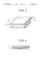
- FIG. 1 is a developed perspective view illustrating the construction of a first embodiment of the liquid crystal display device according to the present invention
- FIG. 2 is a diagrammatic cross-sectional view taken along line A—A of FIG. 1;
- FIG. 3 is a diagrammatic cross-sectional view similar to FIG. 2, illustrating the operation of an illumination light source in the first embodiment of the liquid crystal display device according to the present invention
- FIG. 4 is, a diagrammatic cross-sectional view similar to FIG. 3, illustrating another construction of the illumination light source and the operation thereof in the first embodiment of the liquid crystal display device according to the present invention
- FIG. 5 is a developed perspective view illustrating the construction of a second embodiment of the liquid crystal display device according to the present invention.
- FIG. 6 is a diagrammatic cross-sectional view taken along line B—B of FIG. 5;
- FIG. 7 is a cross-sectional view of a portion of the second embodiment, illustrating the detailed construction of the backlight in the second embodiment of the liquid crystal display device according to the present invention.
- FIG. 8 is a diagrammatic plan view illustrating one example of the arrangement of ridge-like microprisms formed on a surface of a lower transparent hard substrate of the second embodiment of the liquid crystal display device according to the present invention.
- FIG. 9 is a diagrammatic plan view illustrating a third embodiment of the liquid crystal display device according to the present invention, and illustrating one example of a light scattering reflection printed pattern formed on a surface of a lower transparent hard substrate of an illumination-and-touch panel;
- FIG. 10 is a cross-sectional view illustrating an example of a conventional liquid crystal display device provided with a transmission type of liquid crystal panel and a backlighting illumination device, i.e., a so-called backlight;
- FIG. 11 is a cross-sectional view of a liquid crystal display device according to a fourth embodiment of the present invention.
- FIG. 12 is cross-sectional view of a liquid crystal display device according to a fifth embodiment of the present invention.
- FIG. 13 is a plan view illustrating another example of the arrangement of ridge-like microprisms formed on a surface of a lower transparent hard substrate of a sixth embodiment of the liquid crystal display device according to the present invention.
- FIG. 14 is a plan view illustrating another example of the arrangement of a light scattering reflection printed pattern which is formed on a surface of a lower transparent hard substrate of a seventh embodiment of the liquid crystal display device according to the present invention.
- FIG. 15 is an exploded perspective view illustrating the structure of an input device of an eighth embodiment of the liquid crystal display device according to the present invention.
- FIG. 16 is an exploded perspective view of the structure of an input device of a ninth embodiment of the liquid crystal display device according to the present invention.
- FIG. 17 is a cross-sectional view of a liquid crystal display device according to a tenth embodiment of the present invention.
- FIG. 18 is a cross-sectional process flow diagram showing a method of manufacturing an input device of a liquid crystal display device according to an eleventh embodiment of the present invention.
- FIGS. 19 a , 19 b , 19 c , 19 d and 19 e are views showing the external appearance of a liquid crystal display device according to a twelfth embodiment of the present invention.
- FIGS. 20 a is a cross-sectional view taken along line A—A of FIG. 19 a
- FIG. 20 b is a cross-sectional view taken along line B—B of FIG. 19 a
- FIG. 20 c is a cross-sectional view taken along line C—C of FIG. 19 a
- FIG. 20 d is a cross-sectional view taken along line D—D of FIG. 19 a;
- FIG. 21 is a plan view of a liquid crystal display device according to a thirteenth embodiment of the present invention.
- FIG. 22 is a plan view of a liquid crystal display device according to a fourteenth embodiment of the present invention.
- FIG. 23 is a plan view of a liquid crystal display device according to a fifteenth embodiment of the present invention.
- FIG. 24 is a cross-sectional view of a liquid crystal display device according to a sixteenth embodiment of the present invention.
- FIG. 25 is a perspective view showing the external appearance of an information processing apparatus using the liquid crystal display device according to the present invention.
- FIG. 1 is a developed perspective view illustrating the construction of a first embodiment of the liquid crystal display device according to the present invention
- FIG. 2 is a diagrammatic cross-sectional view taken along line A—A of FIG. 1
- Reference numeral 1 denotes a reflection type of liquid crystal panel
- reference numeral 1 A denotes an upper transparent substrate
- reference numeral 1 B denotes a lower transparent substrate
- reference numeral 1 C denotes a polarizer
- reference numeral 1 D denotes a reflector.
- a transparent substrate is used as the lower substrate and the reflector is installed on the back surface of the lower substrate, but reflection processing may also be applied to the inner surface of the lower substrate.
- Reference numeral 2 denotes a light guide plate which is made of acrylic material or the like and constitutes an illumination device
- reference numeral 3 denotes an illumination device
- reference numeral 3 A denotes a linear lamp (a linear light source)
- reference numeral 3 B denotes a reflecting sheet
- reference numeral 4 denotes a touch panel
- reference numeral 4 A denotes a soft film sheet (an upper substrate)
- reference numeral 4 B denotes a hard substrate made of glass, acrylic or the like (a lower substrate; in the present embodiment, a glass plate).
- the illumination device 3 which is formed by the light guide plate 2 made of acrylic material having a of thickness 1.5 mm, the lamp 3 A and the reflecting sheet 3 B stacked on the liquid crystal panel 1 , and the touch panel 4 is stacked on the illumination device 3 .
- the liquid crystal panel 1 is not limited to the shown reflection type of display device, and a semi-transmission type panel can also be used.
- the thickness of the light guide plate 2 is preferably not greater than 1.5 mm.
- the upper surface of the light guide plate 2 i.e., the side thereof closer to the touch panel 4 , has a light-diffusing microprism-, slit- or dot-patterned unevenness or printing 5 (in the present embodiment, dot-patterned printing), and a cold cathode fluorescent tube of diameter 2.0 mm is used as the lamp 3 A which constitutes the light source of the illumination device 3 .
- the diameter of the lamp it is preferable for the diameter of the lamp to be smaller, for example, the diameter is preferably not greater than 2.0 mm.
- the diameter of the lamp 3 A is preferably between 1.6 mm and 2.0 mm if a fluorescent tube is used as the lamp 3 A.
- FIG. 3 is a cross-sectional view similar to FIG. 2, illustrating the operation of an illumination light source in the first embodiment of the liquid crystal display device according to the present invention.
- the touch panel-side surface of the light guide plate 2 which constitutes the illumination device 3 is provided with the dot-patterned printing 5 , and, as shown by arrows in FIG. 3, light from the lamp 3 A is reflected in the direction of the liquid crystal panel 1 and the light reflected from the liquid crystal panel 1 is transmitted through the touch panel 4 and exits on the display-surface side of the liquid crystal display device.
- liquid crystal panel, illumination light source and touch panel are bonded together at their ends by double coated tape.
- the illumination light source may be normally on, but if the illumination light source is to be incorporated in a so-called PDA or a portable information device, such as a notebook personal computer, whose power consumption needs to be controlled, the illumination light source can be constructed to be turned on as required.
- the light guide plate 2 since the light-reflecting pattern of the light guide plate 2 can be formed by printing, the light guide plate 2 is easy to manufacture.
- FIG. 4 is a cross-sectional view similar to FIG. 3, illustrating another construction of the illumination light source and the operation thereof in the first embodiment of the liquid crystal display device according to the present invention.
- a microprism-patterned uneven portion 6 is formed on the touch panel-side surface of the light guide plate 2 which constitutes the illumination device.
- light from the lamp 3 A is reflected and directed in the direction of the liquid crystal panel 1 by the microprism-patterned uneven portion 6 , and the light reflected from the liquid crystal panel 1 is transmitted through the touch panel 4 and exits on the display-surface side of the liquid crystal display device.
- the inclined surface of each microprism prefferably has an angle which enables total reflection of light from the lamp 3 A.
- microprisms may be formed like ridges in the width direction of the light guide plate 2 (in a direction parallel to the linear lamp). According to the present invention, it is possible to reflect the light of the lamp 3 A to the liquid crystal panel 1 with high efficiency. Since the other elements of the construction are similar to that of the first embodiment, the description thereof is omitted.
- FIG. 5 is a developed perspective view illustrating the construction of a second embodiment of the liquid crystal display device according to the present invention
- FIG. 6 is a diagrammatic cross-sectional view taken along line B—B of FIG. 5 .
- an illumination light source and a touch panel which are stacked on the liquid crystal panel 1 are integrated to reduce the thickness of the entire liquid crystal display device.
- Reference numerals which are identical to those used in FIGS. 1 and 2 denote functional portions identical to those of the first embodiment.
- Reference numeral 40 denotes an illumination-and-touch panel
- reference numeral 40 A denotes a transparent soft sheet which serves as the upper substrate of the touch panel
- reference numeral 40 B denotes a transparent hard substrate which serves as both the lower substrate of the touch panel and a light guide plate for the illumination light source.
- This transparent hard substrate 40 B is made of an acrylic plate having a thickness of 1.5 mm, and a surface thereof is processed so that it can diffuse light.
- a polyester film is used as the upper transparent soft substrate 40 A.
- FIG. 7 is cross-sectional view of the essential portion of the second embodiment, illustrating the detailed construction of the second embodiment of the liquid crystal display device according to the present invention.
- the illumination-and-touch panel includes a transparent electrode 40 C formed on the inner surface of the upper transparent soft substrate 40 A which constitutes a touch panel portion between the lower transparent hard substrate 40 B and the upper transparent soft substrate 40 A, a transparent electrode 40 D formed on the inner surface of the lower transparent hard substrate 40 B, and spacers 40 E clamped between both transparent electrodes 40 C and 40 D.
- the upper transparent soft substrate 40 A and the lower transparent hard substrate 40 B are fixed to each other at their ends by a sealing material 7 .
- the construction of the touch panel 40 shown in FIG. 7 resembles that of the liquid crystal panel 1 in that the upper substrate and the lower substrate are bonded together.
- the touch panel 40 differs from the liquid crystal panel 1 in that the lower substrate 40 B is made of a hard material and the upper substrate 40 A is made of a soft material.
- both the upper substrate and the lower substrate need to be made so as not to be easily deformable.
- the present invention also differs from the approach which involves stacking two liquid crystals 1 and using one of them in place of an optical film (to be described later).
- This approach differs from the touch panel 40 of the present invention in that in the liquid crystal used in place of an optical film, to uniformize the thickness of its liquid crystal layer, its upper substrate and its lower substrate need to be made of a material which is not easily deformable.
- An illumination light source portion includes the lower transparent hard substrate 40 B, the lamp 3 A and the reflecting sheet 3 B for effectively using light exiting from the lamp 3 A.
- This lower transparent hard substrate 40 B functions as a light guide plate, and microprisms 8 similar to those shown in FIG. 4, which illustrates the first embodiment, are formed on the upper surface of the lower transparent hard substrate 40 B (which is closer to the touch panel portion), and a transparent resin layer 40 F which is smaller in refractive index than an acrylic plate is formed over the microprisms 8 , i.e., under the transparent electrode 40 D.
- This transparent resin layer 40 F has the function of smoothing the formed surface of the transparent electrode 40 D.
- the illumination device 3 including the lamp 3 A (in the present embodiment, a cold cathode fluorescent tube) and the reflecting sheet 3 B, is installed along one side of the lower transparent hard substrate 40 B.
- This illumination-and-touch panel is stacked on the display surface of the liquid crystal panel 1 , thereby constituting the liquid crystal display device.
- Light which has been generated from the lamp 3 A propagates in the interior of the lower transparent hard substrate 40 B while being reflected in the direction of the liquid crystal panel 1 by the inclined surfaces of the microprisms 8 , as shown by arrows in FIG. 7 .
- the light reflected from the liquid crystal panel 1 is again transmitted through the lower transparent hard substrate 40 B and the illumination-and-touch panel and exits upwardly.
- each of the microprisms which is closer to the lamp 3 A to have an angle which enables total reflection of light from the lamp 3 A.
- These microprisms may be formed like ridges in the width direction of the light guide plate 40 B (in a direction parallel to the lamp). Since the other elements of the construction are similar to those of the first embodiment, the description thereof is omitted.
- the transparent hard substrate 40 B is shared by the hard substrate of the touch panel and the light guide plate of the illumination device, it is possible to reduce the thickness of the liquid crystal display device.
- FIG. 8 is a diagrammatic plan view illustrating one example of the arrangement of the ridge-like microprisms formed on the surface of the lower transparent hard substrate of the second embodiment of the liquid crystal display device according to the present invention. As shown, a multiplicity of ridge-like microprisms 8 are formed in parallel with the longitudinal direction of the lamp 3 A on the upper surface of the lower transparent hard substrate 40 B which constitutes the illumination-and-touch panel. Light from the lamp 3 A is reflected by the inclined surfaces of the ridge-like microprisms 8 and is directed in the direction of the liquid crystal panel.
- the present embodiment it is possible to reflect the light of the lamp 3 A toward the liquid crystal panel 1 with high efficiency, thereby improving the luminance of the liquid crystal-display device.
- the luminance of light with which to illuminate the liquid crystal panel is uniformized by varying the size, specifically, the width, of each of the ridge-like microprisms 8 according to their locations on the lower transparent hard substrate 40 B.
- the width d 3 of a ridge-like microprism 8 which is on a side far from the lamp 3 A is made larger than the width d 1 of a ridge-like microprism 8 which is on a side close to the lamp 3 A.
- the light reflecting surface of the ridge-like microprism 8 is wider on the side far from the lamp 3 A than on the side close to the lamp 3 A, whereby it is possible to prevent a reduction in luminance on the side far from the lamp 3 A.
- an intermediate value between d 1 and d 3 as a width d 2 of a ridge-like microprism 8 which is near the middle of the lower transparent hard substrate 40 B, it is possible to reduce the difference in luminance between the side close to the lamp 3 A, the side far from the lamp 3 A and the position near the middle.
- the distance between adjacent microprisms is constant irrespective of their locations.
- FIG. 9 is a diagrammatic plan view illustrating a third embodiment of the liquid crystal display device according to the present invention, and illustrates one example of a light scattering reflection printed pattern formed on the surface of the lower transparent hard substrate of the touch panel.
- the present embodiment is as a whole similar to the second embodiment shown in FIG. 5, and only the form of the surface treatment formed on the surface of the lower transparent hard substrate of the illumination-and-touch panel differs between the third embodiment and the second embodiment.
- a multiplicity of light scattering reflection printed patterns 9 are formed on the upper surface of the lower transparent hard substrate 40 B which constitutes the illumination-and-touch panel.
- a transparent resin film similar to that shown in FIG. 7 is formed over the light scattering reflection printed patterns 9 .
- the luminance of light with which to illuminate the liquid crystal panel is uniformized by varying the size, specifically, the diameter, of each of the light scattering reflection printed patterns 9 according to their locations on the lower transparent hard substrate 40 B.
- the width d 3 of a light scattering reflection printed pattern 9 which is on a side far from the lamp 3 A is made larger than the width d 1 of the light scattering reflection printed patterns 9 which are on a side close to the lamp 3 A.
- the light scattering surface of the light scattering reflection printed pattern 9 is wider on the side far from the lamp 3 A than on the side close to the lamp 3 A, whereby it is possible to prevent a reduction in luminance on the side far from the lamp 3 A.
- the distance between the adjacent light scattering reflection printed patterns 9 is constant irrespective of their locations.
- the touch panel or the touch panel portion in each of the above-described embodiments is an analog touch panel which identifies a coordinate position in a two-dimensional plane by detecting a variation in resistance due to contact between the transparent electrodes formed between the upper and lower substrates separated from each other by the spacers or a variation in capacitance due to a variation in the space between the transparent electrodes when the upper substrate is pressed.
- the present invention is not limited to the reflection type, and can be similarly applied to the aforementioned semi-transmission type of liquid crystal panel.
- a so-called wedge-shaped substrate whose thickness progressively decreases from a side near that on which the lamp is installed may also be used as the light guide plate which constitutes the illumination device or the lower transparent hard substrate which constitutes the illumination-and-touch panel.
- the liquid crystal panel used in the present invention may be either of a passive matrix type of liquid crystal panel and an active matrix type of liquid crystal panel.
- various kinds of light compensation members, other than the polarizer, which are stacked on the liquid crystal panel, are omitted.
- a cold cathode fluorescent tube is used as a light source which illuminates the liquid crystal panel of the liquid crystal display device
- another type of light source such as a light emitting diode
- a light emitting diode may be installed at an edge of the transparent electrode which constitutes the light guide plate or the illumination-and-touch panel. In this case, it is desirable in terms of visibility for the light emitting diode to have a white color tone.
- FIG. 11 is a cross-sectional view of a liquid crystal display device according to a fourth embodiment of the present invention.
- the linear light source 3 A such as a fluorescent lamp or an LED
- the input device 40 such as the illumination-and-touch panel made of the light guide plate 40 B and the soft film 40 A
- a passive type liquid crystal display panel in which a plurality of signal electrodes (first pixel electrodes) and a plurality of scanning electrodes (second pixel electrodes) intersect in a matrix form.
- the reflecting layer 1 D made from an aluminum thin film, a protective film 1 K made from an oxidation preventing film such as SiO2, and lower electrodes 1 E made from a transparent conductive film such as ITO (Indium Tin Oxide) are formed on the inner surface of the first lower substrate 1 B which is a lower glass substrate.
- a protective film 1 K made from an oxidation preventing film such as SiO2
- lower electrodes 1 E made from a transparent conductive film such as ITO (Indium Tin Oxide) are formed on the inner surface of the first lower substrate 1 B which is a lower glass substrate.
- a lower alignment film 1 M which covers the lower electrodes 1 E is formed over the inner surface of the first lower substrate 1 B.
- R, G, B three-color (R, G, B) color filter 1 J in which a dye or a pigment is added to an organic resin film
- a protective film 1 L made of an organic material for preventing impurities from entering into a liquid crystal layer 1 H from the color filters 1 J and for flattening the inner surface of the second substrate 1 A
- an upper electrode (scanning electrode) 1 F made from a transparent conductive film such as ITO.
- An upper alignment film 1 N which covers the upper electrodes 1 F is formed on the inner surface of the second substrate 1 A.
- a grid- or stripe-shaped light shielding film (black matrix) is formed among individual colors R, G and B which constitute the color filter 1 J, as required, and the protective film 1 L is formed over the light shielding film.
- the liquid crystal layer 1 H made of a liquid crystal composition is injected between these first and second lower substrates 1 B and 1 A and is scaled by a sealing material 1 G such as epoxy resin, thereby constituting the liquid crystal display panel.
- Spacers 1 P for uniformizing the thickness of the liquid crystal layer 1 H arc provided between the first and second lower substrates 1 B and 1 A.
- the polarizer 1 C, a first retardation film 1 S and a second retardation film 1 T are stacked on the outer (upper) surface of the second substrate 1 A which is an observer-side substrate of the liquid crystal display panel.
- An adhesive layer 1 Q made of an adhesive (for example, an epoxy- or acrylic-base adhesive) or a pressure sensitive adhesive is provided between each of the second substrate 1 A, the polarizer 1 C, the first retardation film 1 S and the second retardation film 1 T, whereby the second substrate 1 A, the polarizer 1 C, the first retardation film 1 S and the second retardation film 1 T are fixed to one another.
- pressure sensitive adhesive refers to an adhesive which can again bond together the optical films 1 C, 1 S and 1 T as well as an optical film 1 R even if they separate after having been bonded together.
- the reflecting layer 1 D it is preferable in terms of reflectance for the reflecting layer 1 D to have mirror reflection characteristics, and in the present embodiment, an aluminum film is formed by an evaporation method.
- the surface of the reflecting layer 1 D may be covered with a multi-layer film for improving reflectance, and the protective film 1 K is formed on the multi-layer film for the purposes of protecting the reflecting layer 1 D from corrosion and of flattening the surface thereof
- the reflecting layer 1 D is not limited to aluminum, and may use any film that has mirror reflection characteristics, for example, a metal film such as chromium or silver or a non-metal film.
- the protective film 1 K is not limited to a SiO2 film, and may be any insulation film that protects the reflecting layer 1 D, for example, an inorganic film such as a silicon nitride film, an organic metal film such as an organic titanium film or an organic film such as polyimide or epoxy.
- the organic film such as polyimide or epoxy is superior in terms of flatness, whereby the lower electrodes 1 E can readily be formed on the protective film 1 K. If the organic metal film such as an organic titanium film is used as the protective film 1 K, the lower electrodes 1 E can be formed at a high temperature, whereby the wiring resistance of the lower electrodes 1 E can be lowered.
- the light guide plate 40 B and the lamp 3 A which serve as an illumination device to be used when external light is insufficient are provided above the liquid crystal panel on which a multi-layer optical film 1 V is installed.
- the light guide plate 40 B is made of a transparent resin such as an acrylic resin, and a print pattern or an unevenness pattern for causing light L 4 of the lamp 3 A to exit toward the liquid crystal display panel is formed on the observer-side (upper) surface of the light guide plate 40 B.
- this illumination device is constructed integrally with the input device 40 , such as a touch panel, made of the hard substrate (light guide plate) 40 B and the soft film 40 A.
- the input device 40 detects the position being pressed and outputs a data signal to be sent to a host 50 of an information processing apparatus 47 .
- the second substrate 1 A of the liquid crystal display panel, the light guide plate 40 B and the input device 40 are fixed by double-sided adhesive tape (for example, an unwoven fabric impregnated with a pressure sensitive adhesive).
- double-sided adhesive tape for example, an unwoven fabric impregnated with a pressure sensitive adhesive.
- the lamp 3 A may be omitted.
- the lamp 3 A may be added to the liquid crystal display panel as required.
- the adhesive layer 1 R which is provided between the first retardation film 1 S and the second retardation film 1 T has a light scattering function. Specifically, a light scattering material which differs in refractive index from the adhesive of the adhesive layer 1 R is contained in the adhesive. Because the adhesive and the scattering material differ in refractive index, light is scattered in the adhesive layer 1 R.
- the adhesive and the scattering material of the adhesive layer 1 R need only differ in refractive index, and if an epoxy- or acrylic-adhesive is used as the adhesive, it is possible to use, as the scattering material, transparent organic grains such as polyethylene, polystyrene or divinylbenzene or transparent inorganic grains such as silica.
- the adhesive since the adhesive needs only to differ from the scattering material in refractive index, the previously described pressure sensitive adhesive may also be used. In this case, even if the first retardation film 1 S is mistakenly bonded to the second retardation film 1 T, it is possible to reproduce the first retardation film 1 S and the second retardation film 1 T.
- transparent inorganic or organic grains as the scattering material, it is possible to improve the reflectance or spectral characteristics of the liquid crystal display device because the amount of absorption in the visible radiation range by the transparent inorganic or organic grains is small.
- the adhesive is an organic substance, it is possible to reduce a difference in coefficient of thermal expansion by using organic grains as the scattering material, so that no cracks occur in the adhesive layer 1 R.
- External light (incident light) L 1 such as sunlight which is radiated from various directions reaches the reflecting layer 1 D through the input device 40 made of the soft film 40 A and the light guide plate 40 B, the polarizer 1 C which transmits light along only a particular axis of polarization, the adhesive layer 1 Q for fixing the polarizer 1 C to the first retardation film 1 S, the first retardation film 1 S, the adhesive layer 1 R having the light scattering function and which fixes the second retardation film 1 T to the first retardation film 1 S, the second retardation film 1 T, the adhesive layer 1 Q for fixing the second retardation film 1 T to the second substrate 1 A, the second substrate 1 A, the color filter 1 J, the upper electrodes 1 F, the liquid crystal layer 1 H and a particular pixel electrode (or a particular signal line) 1 Z.
- the external light L 1 which has reached the reflecting layer 1 D is reflected as reflected light L 2 , and the reflected light L 2 reaches the adhesive layer 1 R having the light scattering function, through the reverse path to that of the external light L 1 , i.e., via the particular pixel electrode 1 Z, the liquid crystal layer 1 H, the upper electrodes 1 F, the color filter 1 J, the second substrate 1 A, the adhesive layer 1 Q and the second retardation film 1 T which converts the reflected light L 2 into light which is easy to transmit through the polarizer 1 C, by using a double refraction effect.
- the reflected light L 2 which has entered the adhesive layer 1 R is scattered in various directions to produce scattered light L 3 .
- the direct reflected light L 2 and the scattered light L 3 which have exited from the adhesive layer 1 R are emitted from the liquid crystal display device through the first retardation film 1 S which compensates for a phase difference occurring when light passes through the liquid crystal layer 1 H, by using a double refraction effect, the adhesive layer 1 Q, the polarizer 1 C, the input device 40 made of the light guide plate 40 B and the soft film 40 A.
- An observer can recognize an image display controlled by the particular pixel electrode 1 Z, by viewing the direct reflected light L 2 or the scattered light L 3 emitted from the liquid crystal display device.
- the electrodes 1 E and 1 F of the liquid crystal display device are arranged at intervals of a particular spacing ⁇ . Accordingly, there is also a case in which the liquid crystal electrodes 1 E and 1 F optically function as a diffraction grating.
- FIG. 12 is a cross-sectional view of a liquid crystal display device according to a fifth embodiment of the present invention.
- the reference numerals used in FIG. 12 are identical to those shown in FIG. 11 which has previously been described in the fourth embodiment.
- the fifth embodiment is characterized in that an active matrix liquid crystal display panel using switching elements such as TFTs is used as a liquid crystal display panel.
- a plurality of pixels each having a thin-film transistor TFT 1 and the pixel electrode 1 Z are formed over the inside (liquid-crystal-side) surface of the first substrate 1 B.
- Each of the pixels is disposed within an area of intersection of adjacent scanning signal lines and adjacent video signal lines.
- the thin-film transistor TFT 1 includes a gate electrode GT provided on the first substrate 1 B, a gate insulation film G 1 which overlies the gate electrode GT, a first semiconductor layer (channel layer) As which overlies the gate insulation film GI, a second semiconductor layer (a semiconductor layer which contains impurities) rO which overlies the first semiconductor layer As, and a source electrode SD 1 and a drain electrode SD 2 which overly the second semiconductor layer rO.
- each of the source electrode SD 1 and the drain electrode SD 2 is formed by a multi-layer conductive film indicated at r 1 and r 2 , but may also be formed by only the single-layer conductive film r 1 .
- the relationship between the electrodes SD 1 and SD 2 is inverted so that the electrode SD 2 becomes a source electrode and the electrode SD 1 becomes a drain electrode, but in the following description, the electrodes SD 1 and SD 2 will be referred to for the sake of convenience.
- Reference numeral PSV 1 denotes a protective film made of an insulation film which protects the thin-film transistor TFT 1
- reference numeral 4 a denotes a pixel electrode
- reference numeral 1 M denotes a first alignment film which aligns the side of the liquid crystal layer 1 H that is closer to the first substrate 1 B
- reference numeral IN denotes a second alignment film which aligns the side of the liquid crystal layer 1 H that is closer to the second substrate 1 A
- reference numeral 1 F denotes an upper electrode (common electrode).
- Reference numeral BM denotes a light shielding film which shields the thin-film transistor TFT 1 from light.
- the light shielding film BM is also called a black matrix and also serves the function of shielding the portion between the pixel electrode 1 Z and an adjacent pixel electrode from light and of improving contrast.
- Symbol SIL denotes a conductive film which electrically connects the upper electrode 1 F and a terminal (made of a multi-layer metal film indicated at g 1 , g 2 , r 1 , r 2 and r 3 ) provided on the first substrate 1 B.
- the portion between the source electrode SD 1 and the drain electrode SD 2 conducts electrically and the thin-film transistor TFT 1 functions as a switch.
- the pixel electrode 4 a is electrically connected to the source electrode SD 1
- a video signal line is electrically connected to the drain electrode SD 2
- a scanning signal line is electrically connected to the gate electrode GT, whereby the particular pixel electrode 4 a is selected by a selecting voltage applied to the scanning signal line and a gray scale voltage applied to the video signal line can be supplied to the particular pixel electrode 4 a .
- Symbol Cst denotes a capacitor electrode having the function of holding the gray scale voltage supplied to the pixel electrode 4 a until the next selection period.
- An active matrix type of liquid crystal display device has a number of features. For example, since a switching element such as a thin-film transistor is provided for each pixel, there is no problem of crosstalk occurring between different pixels, and there is no need to eliminate crosstalk by special driving such as an amplitude selective addressing method; it is possible to readily realize a display of multiple gray levels; and even if the number of scanning lines are increased, the contrast is not lowered.
- the particular pixel electrode 1 Z is made of a reflective metal film such as aluminum, chromium, titanium, tantalum, molybdenum or silver.
- the protective film PSV 1 is provided between the particular pixel electrode 1 Z and the thin-film transistor TFT 1 , even if the particular pixel electrode 1 Z is made sufficiently large to overlap the thin-film transistor TFT 1 , no malfunction occurs at all, whereby it is possible to realize a liquid crystal display device having high reflectance.
- the present embodiment differs from the previously-described fourth embodiment in that the first retardation film 1 S is not present and a third retardation film 1 U for improving viewing angle characteristics is provided.
- the other structural features of the optical film 1 V are identical to that of the optical film used in the fourth embodiment.
- the third retardation film 1 U is also called a viewing-angle enlarging film, and is provided for the purpose of improving the dependence of the display characteristics of the liquid crystal display device upon angles by using double refraction characteristics.
- the third retardation film 1 U can also be formed by an organic resin-film such polycarbonate, polyacrylate or polysulfone, it is possible to prevent cracks from occurring in the light scattering adhesive layer 1 R, by using the light scattering adhesive layer 1 R as an adhesive layer which secures the third retardation film 1 U to the second retardation film 1 T.
- a plurality of pixel electrodes 1 Z of the liquid crystal display device are two-dimensionally arranged at intervals of a particular spacing ⁇ , in each of the X and Y directions. Accordingly, there is a case in which the particular pixel electrode 1 Z optically functions as a diffraction grating.
- FIG. 13 is a diagrammatic plan view illustrating another example of the arrangement of the microprisms formed on the surface of the lower transparent hard substrate 40 B of the liquid crystal display device according to the present invention.
- a multiplicity of ridge-like microprisms 8 are formed in parallel with the longitudinal direction of the lamp 3 A on the upper surface of the lower transparent hard substrate 40 B which constitutes an illumination-and-touch panel.
- Light from the lamp 3 A is reflected by the inclined surfaces of the ridge-like microprisms 8 and is directed in the direction of the liquid crystal panel.
- the luminance of light used to illuminate the liquid crystal panel is uniformized by varying the distance between the adjacent ridge-like microprisms 8 according to their locations on the lower transparent hard substrate 40 B.
- a distance ⁇ 3 between ridge-like microprisms 8 which are on a side far from the lamp 3 A is made smaller than a distance ⁇ 1 between microprisms 8 which are on a side close to the lamp 3 A.
- the density of the ridge-like microprisms 8 is higher on the side far from the lamp 3 A than on the side close to the lamp 3 A, it is possible to prevent a reduction in luminance on the side far from the lamp 3 A.
- FIG. 13 there is shown an example in which the ridge-like mnicroprisms 8 have a constant size at any location on the lower transparent hard substrate 40 B.
- the ridge-like microprisms 8 of the lower transparent hard substrate 40 B cause interference fringes between the liquid crystal electrodes 1 E and 1 F, but by setting the distance between the ridge-like microprisms 8 to a value in a range in which no interference fringes occur, and furthermore by varying the ridge-like microprisms 8 in size to adjust the brightness, it is possible to obtain a display with uniform brightness free of interference fringes.
- the other structural features of the sixth embodiment are identical to those of the previously described second embodiment.
- FIG. 14 is a diagrammatic plan view illustrating another example of the arrangement of a light scattering reflection printed pattern which is formed on the surface of the lower transparent hard substrate 40 B of the liquid crystal display device according to the present invention. As shown, a multiplicity of light scattering reflection printed patterns 9 are formed on the upper surface of the lower transparent hard substrate 40 B which constitutes the illumination-and-touch panel. Light from the lamp 3 A is reflected by the light scattering reflection printed patterns 9 and is directed in the direction of the liquid crystal panel.
- the luminance of light used to illuminate the liquid crystal panel is uniformized by varying the distance between the adjacent light scattering reflection printed patterns 9 according to their locations on the lower transparent hard substrate 40 B.
- a distance ⁇ 3 between adjacent light scattering reflection printed patterns 9 which are on a side far from the lamp 3 A is made smaller than a distance ⁇ 1 between adjacent light scattering reflection printed patterns 9 which are on a side close to the lamp 3 A.
- the density of the light scattering reflection printed patterns 9 is higher on the side far from the lamp 3 A than on the side close to the lamp 3 A, it is possible to prevent a reduction in luminance on the side far from the lamp 3 A.
- FIG. 14 there is shown an example in which the light scattering reflection printed patterns 9 have a constant size at any location on the lower transparent hard substrate 40 B.
- the light scattering reflection printed patterns 9 of the lower transparent hard substrate 40 B cause interference fringes between the liquid crystal electrodes 1 E and 1 F, but by setting the distance between the light scattering reflection printed patterns 9 to a value in a range in which no interference fringes occur, and furthermore by varying the size of each of the light scattering reflection printed patterns 9 to adjust brightness, it is possible to obtain a display with uniform brightness free of interference fringes.
- FIG. 15 is an exploded perspective view of a specific input device 40 which constitutes one example of the present invention.
- Reference numeral 40 C denotes second transparent electrodes (Y electrodes) which are formed on the lower surface of the transparent soft sheet 40 A.
- Reference numeral 40 D denotes first electrodes (X electrodes) which are formed on the upper surface of the transparent hard substrate 40 B.
- the Y electrodes 40 C and the X electrodes 40 D are respectively two-dimensionally disposed in orthogonal directions to form XY matrix.
- Reference numeral 7 denotes a fixing member which secures the transparent soft sheet 40 A and the transparent hard substrate 40 B to each other, and a double-sided adhesive tape or an adhesive are used as the fixing member 7 .
- Reference numeral 40 G denotes the terminal of each of the Y electrodes 40 C
- reference numeral 40 H denotes the terminal of each of the X electrodes 40 D.
- the Y electrode terminals 40 G and the X electrode terminals 40 H are respectively connected to terminals 14 C of corresponding flexible connectors 14 , and the input device 40 is connected to the host computer 50 , shown in FIG. 25, via the flexible connectors 14 .
- the host computer 50 can recognize the position coordinates of the pressed point on the transparent soft sheet 40 A.
- the Y electrodes 40 C of the input device 40 are arranged at intervals of a constant spacing ⁇ 5 , the Y electrodes 40 C are regarded as a diffraction grating and may cause interference fringes between the liquid crystal electrodes 1 E or 1 F.
- it is possible to prevent the occurrence of interference fringes by making the spacing ⁇ 5 between the adjacent Y electrodes 40 C equal to the spacing ⁇ , between the adjacent liquid crystal electrodes 1 E or 1 F.
- the X electrodes 40 D of the transparent hard substrate 40 B are arranged at intervals of a constant space ⁇ 4 , the X electrodes 40 D are regarded as a diffraction grating and may cause interference fringes between the liquid crystal electrodes 1 E or 1 F.
- it is possible to prevent the occurrence of interference fringes by making the spacing ⁇ 4 between the adjacent X electrodes 40 D equal to the spacing ⁇ between the adjacent liquid crystal electrodes 1 E or 1 F.
- the input device 40 can also be used as an illumination device.
- Reference numeral 3 C denotes a cable for applying a voltage to the fluorescent lamp 3 A
- reference numeral 3 D denotes a connector for connecting the cable 3 C to an inverter power supply 54 which is shown in FIG. 25 .
- the input device and the illumination device can be integrated in a manner similar to that described previously in connection with the second embodiment.
- terminals 40 T of the input device are preferably provided on a side different from the side on which the light source 3 A of the illumination device is provided.
- the light source 3 A can be positioned without being hindered by the flexible connector 14 .
- FIG. 16 is an exploded perspective view of a specific input device 40 which constitutes one example of the present invention.
- Reference numeral 40 C denotes a second transparent electrode which is formed on the lower surface of the transparent soft sheet 40 A.
- Reference numeral 40 D denotes a first transparent electrode which is formed on the upper surface of the transparent hard substrate 40 B.
- each of the second transparent electrode 40 C and the first transparent electrode 40 D is an integrated resistance film which two-dimensionally covers the whole of a coordinate input area (or display area) 1 S.
- a transparent conductive film such as ITO (Indium Tin Oxide) is used as the resistance film of each of the second transparent electrode 40 C and the first transparent electrode 40 D.
- Reference numerals 40 J and 40 K denote terminals of the first transparent electrode 40 D
- reference numerals 40 L and 40 M denote a terminal of the second transparent electrode 40 C.
- Reference numerals 40 N and 40 P denote lines provided on the transparent hard substrate 40 B, respectively.
- Reference numeral 40 N denotes a line which electrically connects the terminal 40 J and one side which extends in a first direction (X direction) of the first transparent electrode 40 D
- reference numeral 40 P denotes a line which electrically connects the terminal 40 K and the opposite side which extends in the first direction (X direction) of the first transparent electrode 40 D.
- Reference numerals 40 Q and 40 R denote lines provided on the transparent soft sheet 40 A, respectively.
- Reference numeral 40 Q denotes a line which electrically connects the terminal 40 L and one side which extends in a second direction (Y direction) of the second transparent electrode 40 C
- reference numeral 40 R denotes a line which electrically connects the terminal 40 M and the opposite side which extends in the second direction (X direction) of the second transparent electrode 40 C.
- the terminals 40 L and 40 M are provided on the transparent hard substrate 40 B, the line 40 Q and the terminal 40 L as well as the line 40 R and the terminal 40 M are electrically connected to each other by a conductive member such as silver paste.
- the terminals 40 L and 40 M may also be provided on the transparent soft sheet 40 A on which the lines 40 Q and 40 R are provided.
- Conductive films such as silver paste, aluminum, chromium or molybdenum can be used as the lines 40 N and 40 P of the transparent hard substrate 40 B and the lines 40 Q and 40 R of the transparent soft sheet 40 A.
- Conductive films such as silver paste, aluminum, chromium or molybdenum can be used as the lines 40 N and 40 P of the transparent hard substrate 40 B and the lines 40 Q and 40 R of the transparent soft sheet 40 A.
- by forming the patterns of the lines 40 N, 40 P, 40 Q and 40 R by a printing method using silver paste it is possible to facilitate the manufacture of the input device 40 .
- Reference numeral 7 denotes a fixing member which secures the transparent soft sheet 40 A and the transparent hard substrate 40 B to each other, and a double-sided adhesive tape or an adhesive is used as the fixing member 7 .
- the patterns of the lines 40 N, 40 P, 40 Q and 40 R are provided in an area in which the fixing member 7 is provided, it is possible to reduce the peripheral area of the input device 40 and it is also possible to reduce an area (flame area) which does not contribute to the display produced by the liquid crystal display device.
- the first transparent electrode terminals 40 J and 40 K as well as the first transparent electrode terminals 40 L and 40 M are connected to the terminal 14 C of the flexible connector 14 , and the input device 40 is connected to the host computer 50 shown in FIG. 25, via the flexible connector 14 .
- the second transparent electrode 40 C and the first transparent electrode 40 D are electrically connected to each other at the corresponding position, whereby the host computer 50 can recognize the position coordinates of the pressed point on the transparent soft sheet 40 A by measuring the relationship between resistance values R 1 , R 2 , R 3 and R 4 between the connection point and the respective terminals ( 40 J, 40 K, 40 L and 40 M).
- the lines 40 N and 40 P of the transparent hard substrate are respectively connected to the entire corresponding sides of the first transparent electrode 40 D, while the lines 40 Q and 40 R of the transparent soft sheet are respectively connected to the entire corresponding sides of the second transparent electrode 40 C. Accordingly, a difference does not occur in connection resistance between the electrodes and the lines according to the position of a pressed point, whereby the position coordinates of the pressed point can be accurately measured.
- the input device 40 is easy to manufacture.
- the input device 40 can also be used as an illumination device.
- the light source 3 A is provided in the form of a light emitting diode 3 E and a light guide 3 F which guides light emitted from the light emitting diode 3 E and forms a linear light source.
- Reference numeral 3 C denotes a cable for applying a voltage to the light emitting diode 3 E
- reference numeral 3 D denotes a connector for connecting the cable 3 C to a direct-current power supply or a battery 52 , which is shown in FIG. 25 .
- the input device and the illumination device can be integrated in a manner similar to that described previously in connection with the second embodiment.
- the terminal 40 T of the input device is preferably provided on a side different from the side on which the light source 3 A of the illumination device is provided.
- the first transparent electrode terminals 40 J and 40 K and the first transparent electrode terminals 40 L and 40 M are respectively provided on sides different from the side on which the light source 3 A of the input device 40 is provided, the light source 3 A can be positioned without being hindered by the flexible connector 14 .
- FIG. 17 shows another embodiment in which the lamp 3 A and the reflecting sheet 3 B are removed from the second embodiment shown in FIG. 7 .
- the illumination-and-touch panel 40 can be used as a touch panel if the light source such as the lamp 3 A is removed, whereby constituent parts can be made common to illumination-and-touch panels and touch panels.
- FIG. 18 is a process flow diagram showing one example of a method of manufacturing the illumination-and-touch panel 40 of the second embodiment shown in FIG. 7 .
- the uneven pattern 8 for reflecting light is formed on one surface of the transparent hard substrate 40 B.
- acrylic resin, glass or the like may be used for the transparent hard substrate 40 B, acrylic resin is preferable in terms of the easiness of processing thereof.
- Polyethylene terephthalate (PET) can also be used for the transparent hard substrate 40 B if the transparent hard substrate 40 B is made thick to improve the strength thereof.
- the uneven pattern 8 may have recesses, projections or any other shape that is capable of reflecting the light of the lamp 3 A toward the liquid crystal panel (downwardly, in FIG. 18 ).
- the uneven pattern 8 may be formed by press working, cutting or resin molding.
- the transparent resin layer 40 F is formed over the surface of the transparent hard substrate 40 B on which the uneven pattern 8 is formed. Since light is reflected by the uneven pattern 8 , the transparent resin layer 40 F has a refractive index different from that of the transparent hard substrate 40 B. One reason why the transparent resin layer 40 F is provided is to improve the adhesion of the first transparent electrode 40 D to be formed later. Another reason why the transparent resin layer 40 F is provided is to flatten the surface on which the uneven pattern 8 is formed and improve the flatness of the first transparent electrode 40 D, thereby improving the connectivity of the touch panel.
- the material of the transparent resin layer 40 F preferably has good adhesion to the transparent hard substrate 40 B, good transparency, and a refractive index different from that of the transparent hard substrate 40 B.
- an epoxy-base resin, a polyimide-base resin or the like can be used.
- a transparent conductive film such as ITO is formed on the transparent resin layer 40 F, and the transparent conductive film is patterned to form the first transparent electrode 40 D (the first transparent electrode).
- the lines 40 N and 40 P and the terminals 40 J, 40 K, 40 L and 40 M are formed as shown in FIG. 16 .
- Evaporation, low-temperature sputtering and ion plating are available as the method of forming the transparent conductive film over the transparent hard substrate 40 B and the transparent resin layer 40 F, but ion plating is advantageous in terms of manufacturing costs. If acrylic resin is used for the transparent hard substrate 40 B, low-temperature sputtering and ion plating both of which can form an ITO film at a low temperature are available in terms of the problem of heat resistance.
- photoetching is advantageous in terms of the accuracy of the patterns.
- the spacers 40 E are sprayed over the first transparent electrode 40 D.
- Plastic spacers which are insulating substances easily deformable by pressure are used as the spacers 40 E.
- the material of the plastic spacers is polyethylene, polystyrene, divinylbenzene, benzoguanamine resin or the like.
- a method of spraying the spacers 40 E over the transparent hard substrate 40 B and the first transparent electrode 40 D there are a method of mixing the spacers 40 E with a volatile solvent such as alcohol and applying the spacers 40 E (a wet method) and a method of blowing the spacers 40 E by high-pressure air and making the spacers 40 E adhere to the substrate (a dry method).
- a volatile solvent such as alcohol
- the transparent soft sheet 40 A is prepared.
- the material of the transparent soft sheet 40 A may be an insulating substance which is transparent and soft.
- PET polyvinylidene chloride or polyvinyl chloride can be used, PET is advantageous because a subsequent transparent conductive film can easily be formed.
- a transparent conductive film such as ITO is formed on the transparent soft sheet 40 A, and the transparent conductive film is patterned to form the second transparent electrode 40 C (the second transparent electrode).
- the lines 40 Q and 40 R are formed as shown in FIG. 16 .
- Evaporation, low-temperature sputtering and ion plating are available as the method of forming the transparent conductive film over the transparent soft sheet 40 A, but ion plating is advantageous in terms of manufacturing costs.
- photoetching is advantageous in terms of the accuracy of the patterns.
- the transparent hard substrate 40 B and the transparent soft sheet 40 A are superimposed on each other with the first transparent electrode 40 D and the second transparent electrode 40 C being opposed to each other, and are fixed to each other by the fixing member 7 , thereby finishing the input device 40 .
- Double-sided adhesive tape and various adhesives are available as the fixing member 7 , but double-sided adhesive tape is advantageous in terms of the easiness of assembly.
- Double-sided adhesive tape is an unwoven fabric impregnated with an epoxy-base adhesive.
- the lamp 3 A and the reflecting sheet 3 B which are shown in FIG. 7 are attached to the input device 40 , whereby a member in which the input device 40 and the illumination device 3 are integrated is finished.
- FIG. 19 a is a front elevational view of a liquid crystal display device 46 which is assembled and finished, as viewed from the display side thereof
- FIG. 19 b is a front side view
- FIG. 19 c is a rear side view
- FIG. 19 d is a left side view
- FIG. 19 c is a right side view.
- reference numeral 18 denotes an upper case (shield case) made from a metal plate such as stainless steel, iron or aluminum
- reference numeral 20 denotes a first aperture which is formed in the upper case 18 as a display window
- Reference numeral 19 denotes a lower case made from a metal plate such as stainless steel, iron or aluminum, or made of plastics such as polycarbonate or ABS resin.
- Reference numeral 21 denotes claws provided on the upper case 18 and reference numeral 22 denotes hooks provided on the upper case 18 , and the upper case 18 is joined to the lower case 19 with the lower case 19 being fixed by the claws 21 and the hooks 22 .
- Reference numeral 3 A denotes a light source such as a fluorescent lamp or an LED (Light Emitting Diode).
- Reference numeral 40 B denotes a light guide which is made of a transparent material such as acrylic resin or glass and serves to illuminate the liquid crystal display panel with the light of the lamp 3 A.
- the light source 3 A and the light guide 40 B constitutes an illumination device (front light) for supplying light to the liquid crystal display device 46 when external light is insufficient.
- Reference numeral 40 A denotes a soft film.
- the soft film 40 A and the hard substrate (light guide) 40 B constitute the input device (touch panel) 40 for inputting data to be sent to a host (information processing part) connected to the liquid crystal display device 46 .
- Reference numeral 1 V denotes an optical film including the adhesive layer 1 R, the polarizer 1 C, the first retardation film 1 S, the second retardation film 1 T and the like which are provided over the display part of the liquid crystal display device 46 .
- the optical film 1 V is accommodated in the first aperture 20 of the upper case 18 so that the thickness of the liquid crystal display device 46 is reduced.
- FIG. 20 a is a cross-sectional view taken along line A—A of FIG. 19 a
- FIG. 20 b is a cross-sectional view taken along line B—B of FIG. 19 a
- FIG. 20 c is a cross-sectional view taken along fine C—C of FIG. 19 a
- FIG. 20 d is a cross-sectional view taken along line D—D of FIG. 19 a.
- the liquid crystal display panel (liquid crystal cell) is formed by bonding the first substrate 1 B and the second substrate 1 A together.
- a seal member 31 for sealing an injection hole after the liquid crystal layer 1 H is injected into the liquid crystal cell is provided on side walls of the first substrate 1 B and the second substrate 1 A.
- a second aperture 23 is provided in the portion of the upper case 18 which corresponds to the seal member 31 , whereby even if the seal member 31 projects, the external dimensions of the liquid crystal display device can be made small.
- the optical film 1 V including the above-described various layers are fixed to the external (upper) surface of the second substrate 1 A.
- a driving circuit for the liquid crystal display panel which includes a scanning line driving printed circuit board (scanning line driving PCB) 30 , a scanning line driving IC chip 28 , a flexible printed circuit board (TCP) 29 , a signal line driving IC chip 32 and a signal line driving printed circuit board (signal line driving PCB) 33 , is provided at the periphery of the first substrate 1 B and the second substrate 1 A.
- a signal line driving circuit is formed by the signal line driving IC chip 32 , the TCP 29 and the signal line driving PCB 33 , and is connected to the signal lines 1 E of the first substrate 1 B.
- a scanning line driving circuit is formed by the scanning line driving PCB 30 , the scanning line driving IC chip 28 and the TCP 29 , and in the case of a matrix type liquid crystal display device using an amplitude selective addressing method, the scanning line driving circuit is connected to the scanning signal lines 1 F of the second substrate 1 A.
- the scanning line driving circuit is connected to the first substrate 1 B.
- Reference numeral 24 denotes an interface connector for electrically connecting the liquid crystal display device 46 to the host 50 which is an external circuit.
- the interface connector 24 is provided on the scanning line driving PCB 30
- the interface connector 24 may also be provided on the signal line driving PCB 33 .
- the scanning line driving PCB 30 and the signal line driving PCB 33 are electrically connected to each other by connection means.
- Reference numeral 26 denotes a spacer for securing the scanning line driving PCB 30 .
- Reference numeral 27 denotes a spacer for securing the portion for connection between the liquid crystal display panel and the scanning line driving circuit as well as the signal line driving circuit, and the spacer 27 is made of an insulating elastic material such as rubber.
- Reference numeral 25 denotes double-sided adhesive tape, and, for example, an unwoven fabric impregnated with an epoxy-base adhesive can be used as the double-sided adhesive tape 25 .
- the liquid crystal display panel is fixed to the upper case 18 by the double-sided adhesive tape 25 .
- the double-sided adhesive tape 25 is also used for fixing the light guide 40 B and the soft film 40 A of the illumination-and-input device 40 to the upper case 18 .
- the assembly of the liquid crystal display device is made easy so that even if the individual members are erroneously fixed, they can be readjusted, and so the manufacturing yield of the liquid crystal display device is improved.
- An uneven pattern for securing the liquid crystal panel is formed on the lower case 19 .
- FIG. 21 shows an example in which the light source 3 A is used as a fluorescent tube in the previously-described twelfth embodiment.
- the light source 3 A is provided on a shorter side of the input device 40 .
- Reference numeral 3 C′ denotes a lower-voltage cable of the light source 3 A
- reference numeral 3 C′′ denotes a higher-voltage cable of the light source 3 A
- reference numeral 3 D denotes a connector for the cables 3 C′ and 3 C′′.
- the terminal 40 T and the connector 14 for a touch panel are provided on the side of the light guide plate 40 on which the light source 3 A is not provided.
- FIG. 22 shows an example in which the light emitting diode 3 E is used as a light source in the previously-described twelfth embodiment.
- Reference numeral 3 F denotes a light guide for converting the light of the light emitting diode 3 E into linear light.
- the light guide 3 F for the light emitting diode 3 E is provided on a shorter side of the light guide plate 40 .
- Reference numeral 3 C′ denotes a lower-voltage cable of the light emitting diode 3 E
- reference numeral 3 C′′ denotes a higher-voltage cable of the light emitting diode 3 E.
- the interface connector 24 can also be used as a connector for the light emitting diode 3 E.
- the terminal 40 T and the connector 14 for a touch panel are provided on the side of the light guide plate 40 B on which neither the light emitting diode 3 E nor the light guide 3 F is provided.
- FIG. 23 shows another example in which the light emitting diode 3 E is used as a light source in the previously-described twelfth embodiment.
- Reference numeral 3 F denotes a light guide for converting the light of the light emitting diode 3 E into a linear light source.
- the light guide 3 F for the light emitting diode 3 E is provided on a longer side of the light guide plate 40 B.
- Reference numeral 3 C′ denotes a lower-voltage cable of the light emitting diode 3 E
- reference numeral 3 C′′ denotes a higher-voltage cable of the light emitting diode 3 E.
- the interface connector 24 can also be used as a connector for the light emitting diode 3 E.
- the terminal 40 T and the connector 14 for a touch panel are provided on the side of the light guide plate 40 B on which neither the light emitting diode 3 E nor the light guide 3 F is provided.
- the light guide 3 F for the light emitting diode 3 E is provided on a side of the light guide plate 40 B which is different from the side adjacent to the interface connector 24 . Accordingly, in the present embodiment, terminals can be provided on the side adjacent to the interface connector 24 , and the terminal 40 T of the input device 40 and a data terminal 35 of the interface connector 24 can be connected to each other by a flexible connector, whereby the interface connector 24 can be used as connection means common to a liquid crystal driving circuit and the input device 40 .
- the interface connector 24 is also used as the connector for the light emitting diode 3 E, the connection between an information processing apparatus and the host 50 can be realized by the interface connector 24 alone, whereby the size and reliability of the information processing apparatus can be improved.
- FIG. 24 shows an embodiment of a liquid crystal display device in which the input device 40 manufactured by the method shown in FIG. 18 as the eleventh embodiment, the illumination device 3 manufactured separately from the input device 40 , and the liquid crystal panel 1 are assembled in a superimposed manner.
- the illumination-and-input device 40 can be used as a touch panel if a light source such as the light source 3 A is removed, the illumination device 3 manufactured separately and the liquid crystal panel 1 can be superimposed on each other to realize a liquid crystal display device having an illumination device and an input device.
- Double-sided adhesive tape can be used as the means 7 for fixing the individual members.
- the effect of integrating the input device and the illumination device is not obtained, but since the transparent resin layer 40 F is provided between the transparent hard substrate 40 B such as acrylic resin and the first transparent electrode 40 D made of ITO or the like, it is possible to obtain the effect of flattening the surface of the transparent electrode 40 D, the effect of uniformizing the film thickness of the transparent electrode 40 D and also uniformizing the electrical resistivity thereof, and the effect of preventing the transparent electrode 40 D from peeling off. Accordingly, in the present embodiment, the input device 40 having high reliability can be used with the liquid crystal display device.
- the transparent electrode 40 D is provided on a flat surface of the transparent resin layer 40 F provided on the transparent hard substrate 40 B, the film thickness of the transparent electrode 40 D can be uniformized and also the electrical resistivity thereof can be uniformized.
- the accuracy of recognition of position coordinates becomes higher.
- the input device 40 since the input device 40 is not used as an illumination device, neither the uneven pattern 8 nor the reflection printed pattern 9 is provided on the transparent hard substrate 40 B.
- the uneven pattern 8 or the reflection printed pattern 9 is provided on the light guide plate 2 of the illumination device 3 . Furthermore, if a second transparent resin layer 40 S is provided over the uneven pattern 8 or the reflection printed pattern 9 of the light guide plate 2 , the reflectance of the light guide plate 2 is improved and the luminance of the liquid crystal display device is improved.
- the material of the second transparent resin layer 40 S may be any material that has a refractive index different from that of the light guide plate 2 . If the light guide plate 2 is formed of an acrylic resin, a polyimide resin or an acrylic-base resin can be used.
- FIG. 25 is a perspective view showing the external appearance of the information processing apparatus 47 using the liquid crystal display device 46 according to the present invention.
- Reference numeral 48 denotes a display part of the information processing apparatus 47
- reference numeral 49 denotes a keyboard part
- reference numeral 50 denotes a host which performs information processing for the information processing apparatus 47
- reference numeral 51 denotes a microprocessor
- reference numeral 52 denotes a battery
- reference numeral 53 denotes an interface cable which connects the liquid crystal display device 46 and the host computer 50
- reference numeral 54 denotes an inverter power supply for an illumination device
- reference numeral 55 denotes a cable which connects the inverter power supply 54 and a light source 14 of the illumination device
- reference numeral 56 denotes a mobile telephone
- reference numeral 61 denotes a cable which connects the mobile telephone 60 and the information processing apparatus 47 .
- the liquid crystal display device 46 is provided in the display part 48 of the information processing apparatus 47 .
- characters 58 can be inputted or an icon 59 can be selected to execute a function of the software, by pressing a predetermined portion with the pen 56 or a finger.
- the liquid crystal display device 46 of the present applied example is of a reflection type, the power consumption can be reduced by turning off the switch of the inverter power supply 54 when there is external light such as sunlight, so that a consumption of the power of the battery 52 can be lessened.
- the liquid crystal display device 46 can be made thin, small and light-weight
- the information processing apparatus 47 can also be made thin, small and light-weight.
- a reflection or stylus type of liquid crystal display device in which a touch panel is stacked on the display surface of its liquid crystal panel and its entire effective display area, is uniformly illuminated by a front illumination system so that a high-quality image display can be obtained and the brightness of a screen is improved.
Abstract
Description
Claims (15)
Priority Applications (1)
| Application Number | Priority Date | Filing Date | Title |
|---|---|---|---|
| US10/102,911 US7068261B2 (en) | 1998-07-14 | 2002-03-22 | Liquid crystal display device with a touch panel |
Applications Claiming Priority (2)
| Application Number | Priority Date | Filing Date | Title |
|---|---|---|---|
| JP19899898 | 1998-07-14 | ||
| JP10-198998 | 1998-07-14 |
Related Child Applications (1)
| Application Number | Title | Priority Date | Filing Date |
|---|---|---|---|
| US10/102,911 Continuation US7068261B2 (en) | 1998-07-14 | 2002-03-22 | Liquid crystal display device with a touch panel |
Publications (1)
| Publication Number | Publication Date |
|---|---|
| US6456279B1 true US6456279B1 (en) | 2002-09-24 |
Family
ID=16400409
Family Applications (2)
| Application Number | Title | Priority Date | Filing Date |
|---|---|---|---|
| US09/352,359 Expired - Lifetime US6456279B1 (en) | 1998-07-14 | 1999-07-13 | Liquid crystal display device with a touch panel |
| US10/102,911 Expired - Fee Related US7068261B2 (en) | 1998-07-14 | 2002-03-22 | Liquid crystal display device with a touch panel |
Family Applications After (1)
| Application Number | Title | Priority Date | Filing Date |
|---|---|---|---|
| US10/102,911 Expired - Fee Related US7068261B2 (en) | 1998-07-14 | 2002-03-22 | Liquid crystal display device with a touch panel |
Country Status (4)
| Country | Link |
|---|---|
| US (2) | US6456279B1 (en) |
| JP (1) | JP2000215747A (en) |
| KR (2) | KR100316194B1 (en) |
| TW (1) | TW523627B (en) |
Cited By (85)
| Publication number | Priority date | Publication date | Assignee | Title |
|---|---|---|---|---|
| US20010005200A1 (en) * | 1999-12-22 | 2001-06-28 | Daisuke Suzuki | Resistance film type touch panel with short circuit preventing structure |
| US20020001400A1 (en) * | 2000-04-26 | 2002-01-03 | Shunpei Yamazaki | System for identifying an individual, a method for identifying an individual or a business method |
| US20020005922A1 (en) * | 2000-05-12 | 2002-01-17 | Nitto Denko Corporation | Reflection type liquid-crystal display device |
| US20020049714A1 (en) * | 2000-05-11 | 2002-04-25 | Shunpei Yamazaki | Communication system |
| US20020052192A1 (en) * | 2000-05-09 | 2002-05-02 | Shunpei Yamazaki | User identity authentication system and user identity authenication method and mobile telephonic device |
| US20020054261A1 (en) * | 2000-09-18 | 2002-05-09 | Kanetaka Sekiguchi | Liquid crystal display device |
| US20020085131A1 (en) * | 2000-12-29 | 2002-07-04 | Peter Sladen | Display window and assembly |
| US20020106182A1 (en) * | 2001-02-02 | 2002-08-08 | Minebea Co., Ltd. | Spread illuminating apparatus with cover provided over transparent substrate |
| US20030011720A1 (en) * | 2001-07-13 | 2003-01-16 | Satoshi Kawashima | Touch panel for display device with pet film having transparent gel layer |
| US6529188B1 (en) * | 2000-03-06 | 2003-03-04 | Hitachi, Ltd. | Touch panel and screen input type liquid crystal display device |
| US20030043315A1 (en) * | 2001-08-22 | 2003-03-06 | Nitto Denko Corporation | Liquid-crystal dispaly device |
| US20030048597A1 (en) * | 2001-09-07 | 2003-03-13 | Shih-Chieh Wang | Personal digital assistant with waterproof and dustproof functions |
| US6538644B1 (en) * | 1999-11-19 | 2003-03-25 | Fujitsu Takamisawa Component Ltd. | Touch panel |
| US20030122801A1 (en) * | 2001-12-27 | 2003-07-03 | Lg.Philips Lcd Co., Ltd. | Liquid crystal panel device having a touch panel and method of fabricating the same |
| US20030147041A1 (en) * | 2001-12-27 | 2003-08-07 | Lg.Philips Lcd Co., Ltd | Method of fabricating liquid crystal display apparatus integrated with film type touch panel |
| US20030184514A1 (en) * | 2002-03-28 | 2003-10-02 | Henry Grosfeld | Information input display device |
| US6639632B2 (en) * | 2001-07-25 | 2003-10-28 | Huang-Chung Cheng | Backlight module of liquid crystal display |
| US20030227446A1 (en) * | 2002-06-10 | 2003-12-11 | Smk Corporation | Touch-type input apparatus |
| US6665037B2 (en) | 2000-06-15 | 2003-12-16 | Seiko Epson Corporation | Electro-optic device and electronic apparatus |
| US6680448B2 (en) * | 2001-01-18 | 2004-01-20 | Minebea Co., Ltd. | Touch panel for display device |
| US20040032401A1 (en) * | 2002-08-19 | 2004-02-19 | Fujitsu Limited | Touch panel device |
| US20040080483A1 (en) * | 2000-12-28 | 2004-04-29 | Yoshitaka Chosa | Touch panel-integrated reflection type lcd device and electronic device |
| US6738118B2 (en) * | 2001-03-17 | 2004-05-18 | Samsung Electronics Co., Ltd. | Liquid crystal display device |
| US20040109171A1 (en) * | 2002-11-29 | 2004-06-10 | Huang Chuan De | Locating device for measuring distances between dots of a light guide plate and method for using same |
| US20040125430A1 (en) * | 2002-07-04 | 2004-07-01 | Yasushi Kasajima | Display device and electronic equipment having the same |
| US6768259B2 (en) * | 2000-06-13 | 2004-07-27 | Sony Corporation | Display apparatus |
| US20040174694A1 (en) * | 2003-03-04 | 2004-09-09 | Wei-Hsiang Huang | Planar-light apparatus with a non -straight direction light module and a light-guiding plate |
| US20040246743A1 (en) * | 2001-06-30 | 2004-12-09 | Lee Moon-Gyu | Backlight using planar hologram for flat display device |
| US20050030728A1 (en) * | 2001-11-09 | 2005-02-10 | Satoshi Kawashima | Touch panel assembly |
| US20050068291A1 (en) * | 2003-09-30 | 2005-03-31 | International Business Machines Corporation | On demand calibration of imaging displays |
| US6894738B2 (en) * | 2001-03-05 | 2005-05-17 | Nec Lcd Technologies, Ltd. | Lamp unit, light guide plate, liquid crystal display, and method for assembling them |
| US20050140835A1 (en) * | 2002-11-29 | 2005-06-30 | Fujitsu Limited | Illuminating device and liquid crystal display apparatus |
| US20050200772A1 (en) * | 2004-02-27 | 2005-09-15 | Heyg-Kyu Song | Front lighted micro-LCD |
| US20050259082A1 (en) * | 2002-08-13 | 2005-11-24 | Fujitsu Siemens Computers Gmbh | Display device |
| US6972753B1 (en) | 1998-10-02 | 2005-12-06 | Semiconductor Energy Laboratory Co., Ltd. | Touch panel, display device provided with touch panel and electronic equipment provided with display device |
| US6982432B2 (en) * | 2000-01-31 | 2006-01-03 | Nitto Denko Corporation | Touch type liquid-crystal display device and input detecting method |
| US20060008578A1 (en) * | 2004-07-09 | 2006-01-12 | Jin-Shou Fang | Method of fabricating electrode structure of field-emission display |
| US20070002192A1 (en) * | 2005-06-29 | 2007-01-04 | Casio Computer Co., Ltd. | Liquid crystal display apparatus including touch panel |
| US7268770B1 (en) * | 1998-01-09 | 2007-09-11 | Nissha Printing Co., Ltd. | Liquid crystal display of touch input type, and method of manufacture |
| US20080018838A1 (en) * | 2006-07-24 | 2008-01-24 | Nec Lcd Technologies, Ltd. | Color filter substrate, color liquid crystal display device using the same, and method for repairing the same |
| US20080055270A1 (en) * | 2006-09-05 | 2008-03-06 | Jong-Whan Cho | Touch screen display having touch panel, and method of manufacture |
| US20080129647A1 (en) * | 2000-11-30 | 2008-06-05 | Palm, Inc. | Multi-sided display for portable computer |
| US20080316769A1 (en) * | 2007-06-22 | 2008-12-25 | Minebea Co., Ltd. | Spread illuminating apparatus |
| US20090011197A1 (en) * | 2007-06-26 | 2009-01-08 | Tsutomu Matsuhira | Electronic device |
| US7498533B1 (en) * | 2008-02-27 | 2009-03-03 | Silitek Electronic(Guangzhou)Co.,Ltd. | Keypad device |
| US20090161060A1 (en) * | 2007-12-25 | 2009-06-25 | Wintek Corporation | Touch panel and driving method thereof |
| US20090296194A1 (en) * | 2004-09-27 | 2009-12-03 | Idc, Llc | Optical films for directing light towards active areas of displays |
| US7706050B2 (en) | 2004-03-05 | 2010-04-27 | Qualcomm Mems Technologies, Inc. | Integrated modulator illumination |
| US7719747B2 (en) | 2004-09-27 | 2010-05-18 | Qualcomm Mems Technologies, Inc. | Method and post structures for interferometric modulation |
| US7733439B2 (en) | 2007-04-30 | 2010-06-08 | Qualcomm Mems Technologies, Inc. | Dual film light guide for illuminating displays |
| US7750886B2 (en) | 2004-09-27 | 2010-07-06 | Qualcomm Mems Technologies, Inc. | Methods and devices for lighting displays |
| US7766498B2 (en) | 2006-06-21 | 2010-08-03 | Qualcomm Mems Technologies, Inc. | Linear solid state illuminator |
| US7777954B2 (en) | 2007-01-30 | 2010-08-17 | Qualcomm Mems Technologies, Inc. | Systems and methods of providing a light guiding layer |
| US7807488B2 (en) | 2004-09-27 | 2010-10-05 | Qualcomm Mems Technologies, Inc. | Display element having filter material diffused in a substrate of the display element |
| US7845841B2 (en) | 2006-08-28 | 2010-12-07 | Qualcomm Mems Technologies, Inc. | Angle sweeping holographic illuminator |
| US7852430B1 (en) * | 2001-11-29 | 2010-12-14 | Palm, Inc. | Light guide spacers for backlighting a reflective display |
| US7855827B2 (en) | 2006-10-06 | 2010-12-21 | Qualcomm Mems Technologies, Inc. | Internal optical isolation structure for integrated front or back lighting |
| US7859518B1 (en) | 2001-06-04 | 2010-12-28 | Palm, Inc. | Interface for interaction with display visible from both sides |
| US7864395B2 (en) | 2006-10-27 | 2011-01-04 | Qualcomm Mems Technologies, Inc. | Light guide including optical scattering elements and a method of manufacture |
| US7933475B2 (en) | 2006-02-17 | 2011-04-26 | Qualcomm Mems Technologies, Inc. | Method and apparatus for providing back-lighting in a display device |
| US20110128256A1 (en) * | 2009-11-27 | 2011-06-02 | Coretronic Corporation | Light guide apparatus and optical touch display apparatus |
| US20110157093A1 (en) * | 2009-12-29 | 2011-06-30 | Qualcomm Mems Technologies, Inc. | Illumination device with metalized light-turning features |
| US20110193790A1 (en) * | 2010-02-11 | 2011-08-11 | Teh-Zheng Lin | Touch panel module with illumination function |
| US20110234525A1 (en) * | 2001-01-30 | 2011-09-29 | Gettemy Shawn R | Single piece top surface display layer and integrated front cover for an electronic device |
| US20110248922A1 (en) * | 2010-04-09 | 2011-10-13 | Microsoft Corporation | Adaptive keyboard light pillar |
| US8040589B2 (en) | 2008-02-12 | 2011-10-18 | Qualcomm Mems Technologies, Inc. | Devices and methods for enhancing brightness of displays using angle conversion layers |
| US8045252B2 (en) | 2004-02-03 | 2011-10-25 | Qualcomm Mems Technologies, Inc. | Spatial light modulator with integrated optical compensation structure |
| US8049951B2 (en) | 2008-04-15 | 2011-11-01 | Qualcomm Mems Technologies, Inc. | Light with bi-directional propagation |
| US8107155B2 (en) | 2006-10-06 | 2012-01-31 | Qualcomm Mems Technologies, Inc. | System and method for reducing visual artifacts in displays |
| US8134534B1 (en) | 2001-05-22 | 2012-03-13 | Hewlett-Packard Development Company, L.P. | High transparency integrated enclosure touch screen assembly for a portable hand held device |
| US20120113027A1 (en) * | 2010-11-08 | 2012-05-10 | Song Sung-Hoon | Liquid crystal display integrated touch screen panel |
| US20130021297A1 (en) * | 2011-07-18 | 2013-01-24 | Michael Lee | Touch panel |
| US8384674B1 (en) | 2001-01-30 | 2013-02-26 | Hewlett-Packard Development Company, L.P. | Integrated enclosure/touch screen assembly |
| US20130127784A1 (en) * | 2011-11-22 | 2013-05-23 | Qualcomm Mems Technologies, Inc. | Methods and apparatuses for hiding optical contrast features |
| US8692948B2 (en) | 2010-05-21 | 2014-04-08 | Apple Inc. | Electric field shielding for in-cell touch type thin-film-transistor liquid crystal displays |
| US8798425B2 (en) | 2007-12-07 | 2014-08-05 | Qualcomm Mems Technologies, Inc. | Decoupled holographic film and diffuser |
| US8848294B2 (en) | 2010-05-20 | 2014-09-30 | Qualcomm Mems Technologies, Inc. | Method and structure capable of changing color saturation |
| US8872085B2 (en) | 2006-10-06 | 2014-10-28 | Qualcomm Mems Technologies, Inc. | Display device having front illuminator with turning features |
| US8902484B2 (en) | 2010-12-15 | 2014-12-02 | Qualcomm Mems Technologies, Inc. | Holographic brightness enhancement film |
| US8979349B2 (en) | 2009-05-29 | 2015-03-17 | Qualcomm Mems Technologies, Inc. | Illumination devices and methods of fabrication thereof |
| US9019183B2 (en) | 2006-10-06 | 2015-04-28 | Qualcomm Mems Technologies, Inc. | Optical loss structure integrated in an illumination apparatus |
| US9025235B2 (en) | 2002-12-25 | 2015-05-05 | Qualcomm Mems Technologies, Inc. | Optical interference type of color display having optical diffusion layer between substrate and electrode |
| US20150205033A1 (en) * | 2014-01-23 | 2015-07-23 | Qualcomm Mems Technologies, Inc. | Integrating color filters into frontlight for reflective display |
| USD742841S1 (en) * | 2013-03-26 | 2015-11-10 | Sony Corporation | Touch sensitive device |
| EP3486757A3 (en) * | 2017-11-15 | 2019-07-10 | Fujitsu Component Limited | Film and input device |
Families Citing this family (73)
| Publication number | Priority date | Publication date | Assignee | Title |
|---|---|---|---|---|
| JP2002189151A (en) * | 2000-10-11 | 2002-07-05 | Matsushita Electric Ind Co Ltd | Optical receiving module, optical transmitting and receiving module, and method for manufacturing |
| JP3962579B2 (en) * | 2001-03-19 | 2007-08-22 | シャープ株式会社 | Illumination device and reflective liquid crystal display device including the same |
| JP3484497B2 (en) * | 2001-08-10 | 2004-01-06 | ミネベア株式会社 | Planar lighting device |
| KR100416198B1 (en) * | 2001-11-06 | 2004-01-31 | 주식회사 이너텍 | Apparatus of LCD back light |
| US7242393B2 (en) * | 2001-11-20 | 2007-07-10 | Touchsensor Technologies Llc | Touch sensor with integrated decoration |
| KR100443834B1 (en) * | 2001-12-27 | 2004-08-09 | 엘지.필립스 엘시디 주식회사 | Liquid Crystal Display Module Integrated Touch Panel Using the Double Top Case And Assembling Method Thereof |
| CN101261339A (en) * | 2002-03-14 | 2008-09-10 | 日本电气株式会社 | Optical modulating/display device, production method therefor and display apparatus equipped with the optical modulating/displaying device |
| JP2003335464A (en) * | 2002-05-20 | 2003-11-25 | Toshiba Elevator Co Ltd | Elevator operation panel and elevator equipped with it |
| JP4063591B2 (en) | 2002-05-29 | 2008-03-19 | Nec液晶テクノロジー株式会社 | Reflective liquid crystal display |
| US20040017347A1 (en) * | 2002-07-29 | 2004-01-29 | Hougham Gareth G. | Method for fabricating color pixels without light filters |
| KR100457087B1 (en) * | 2002-09-11 | 2004-11-12 | 현대모비스 주식회사 | structure for breaking refracted light and preventing VFD from moving |
| JP4126610B2 (en) * | 2002-12-26 | 2008-07-30 | エルジー ディスプレイ カンパニー リミテッド | Liquid crystal display |
| TWI341983B (en) * | 2003-02-12 | 2011-05-11 | Nissha Printing | Touch panel |
| US20040264192A1 (en) * | 2003-05-06 | 2004-12-30 | Seiko Epson Corporation | Light source apparatus, method of manufacture therefor, and projection-type display apparatus |
| KR100981630B1 (en) * | 2003-11-17 | 2010-09-10 | 삼성전자주식회사 | Liquid crystal display apparatus |
| EP1738250A2 (en) * | 2004-04-14 | 2007-01-03 | Koninklijke Philips Electronics N.V. | Touch sensitive display |
| EP1807162A2 (en) * | 2004-11-05 | 2007-07-18 | Mattel, Inc. | Multi-user touch-responsive entertainment device |
| KR20060116102A (en) * | 2005-05-09 | 2006-11-14 | 삼성전자주식회사 | Back light assembly and display device having the same |
| KR100629053B1 (en) | 2005-05-19 | 2006-09-26 | 삼성전자주식회사 | Key-pad assembly |
| KR100683791B1 (en) * | 2005-07-30 | 2007-02-20 | 삼성에스디아이 주식회사 | Thin film transistor substrate and flat panel display apparatus |
| JP4917840B2 (en) * | 2006-06-05 | 2012-04-18 | シチズン電子株式会社 | Seat switch module |
| US20080030484A1 (en) * | 2006-08-07 | 2008-02-07 | Samsung Electronics Co., Ltd. | Dual liquid crystal display having touch screen |
| KR100805154B1 (en) * | 2006-09-15 | 2008-02-21 | 삼성에스디아이 주식회사 | Organic light emitting display and method of manufacturing the same |
| JP4775247B2 (en) * | 2006-12-21 | 2011-09-21 | 三菱電機株式会社 | Position detection device |
| KR101330697B1 (en) * | 2006-12-21 | 2013-11-18 | 삼성디스플레이 주식회사 | Display device |
| JP5134327B2 (en) * | 2007-09-26 | 2013-01-30 | 株式会社ジャパンディスプレイイースト | Display device |
| JP5024793B2 (en) * | 2007-10-19 | 2012-09-12 | Nltテクノロジー株式会社 | Display device |
| CN101464763B (en) * | 2007-12-21 | 2010-09-29 | 清华大学 | Production method of touch screen |
| US8574393B2 (en) * | 2007-12-21 | 2013-11-05 | Tsinghua University | Method for making touch panel |
| JP2009193233A (en) * | 2008-02-13 | 2009-08-27 | Hitachi Displays Ltd | Display device having touch panel |
| DE102008029567A1 (en) * | 2008-06-21 | 2010-01-07 | Preh Gmbh | Illuminated capacitive proximity sensor |
| PL2141809T3 (en) | 2008-07-03 | 2020-03-31 | Somfy Activites Sa | Electrical switchgear such as a terminal for construction comprising an electrical component |
| FR2933554B1 (en) * | 2008-07-03 | 2012-08-31 | Somfy Sas | ELECTRONIC SWITCH CONTROLLING A DOMOTIC DEVICE |
| TW201003498A (en) * | 2008-07-04 | 2010-01-16 | Wintek Corp | Resistive touch panel with multi-touch recognition ability |
| JP2011222120A (en) * | 2008-08-13 | 2011-11-04 | Sunarrow Ltd | Illuminated key sheet |
| US20100103140A1 (en) * | 2008-10-27 | 2010-04-29 | Sony Ericsson Mobile Communications Ab | Touch sensitive device using optical gratings |
| TWI398810B (en) * | 2008-11-04 | 2013-06-11 | Wintek Corp | Multi-touch resistive touch panel and detecting method and electronic device using the same |
| TW201024820A (en) * | 2008-12-24 | 2010-07-01 | Coretronic Corp | Light-guiding plate and backlight module |
| US8730212B2 (en) * | 2009-08-21 | 2014-05-20 | Microsoft Corporation | Illuminator for touch- and object-sensitive display |
| US8854313B2 (en) * | 2009-12-28 | 2014-10-07 | Polymatech Co., Ltd. | Sensor-integrated illuminated key sheet |
| CN102243544B (en) * | 2010-05-12 | 2013-08-14 | 群康科技(深圳)有限公司 | Touch screen, touch screen manufacturing method and touch display device |
| KR101084848B1 (en) * | 2010-08-26 | 2011-11-21 | 삼성전기주식회사 | Touch screen |
| KR101226936B1 (en) * | 2010-11-10 | 2013-01-30 | 주식회사 엘지화학 | Optical member and method for manufacturing the same and backlight using the optical member, and method for manufacturing the same |
| US9223445B2 (en) | 2010-12-02 | 2015-12-29 | Atmel Corporation | Position-sensing and force detection panel |
| KR20130128439A (en) * | 2010-12-21 | 2013-11-26 | 쓰리엠 이노베이티브 프로퍼티즈 컴파니 | Articles having optical adhesives and method of making same |
| KR101328398B1 (en) | 2011-01-03 | 2013-11-13 | 크루셜텍 (주) | Pointing Device using Radio Frequency |
| JP2012256558A (en) * | 2011-06-10 | 2012-12-27 | Meitaku Kogyo Kk | Large-size surface light source device |
| US20130141341A1 (en) * | 2011-12-06 | 2013-06-06 | Htc Corporation | Handheld electronic device |
| WO2013089161A1 (en) * | 2011-12-13 | 2013-06-20 | 日立化成株式会社 | Liquid curable resin composition, method for manufacturing image display device using same, and image display device |
| TWI451312B (en) * | 2011-12-19 | 2014-09-01 | Pixart Imaging Inc | Optical touch device and light source assembly |
| TWI450153B (en) * | 2012-06-22 | 2014-08-21 | Wintek Corp | Touch panel device |
| US9036109B2 (en) | 2012-08-20 | 2015-05-19 | Apple Inc. | Electronic device with thermally matched light guide plate |
| US9041686B2 (en) * | 2012-08-30 | 2015-05-26 | Amazon Technologies, Inc. | Electronic device component stack |
| KR101552994B1 (en) * | 2012-08-31 | 2015-09-15 | 엘지디스플레이 주식회사 | Organic Emitting Display Device and Method for Manufacturing the Same |
| TWI463477B (en) * | 2012-12-26 | 2014-12-01 | Univ Nat Cheng Kung | Bin allocation method of point light sources for constructing light source sets and computer program product thereof |
| US20140184522A1 (en) * | 2012-12-28 | 2014-07-03 | Wintek Corporation | Touch-sensitive display panel |
| US20140192006A1 (en) * | 2013-01-04 | 2014-07-10 | Amazon Technologies, Inc. | Touch sensor integrated with a light guide |
| US9423897B2 (en) * | 2013-04-01 | 2016-08-23 | Apple Inc. | Electronic device display with shielding layer |
| US9731477B1 (en) * | 2013-08-28 | 2017-08-15 | Amazon Technologies, Inc. | Display stack formed to minimize substrate warping |
| US9134763B2 (en) * | 2013-11-11 | 2015-09-15 | Symbol Technologies, Llc | Externally mounted display device |
| WO2015083030A1 (en) * | 2013-12-02 | 2015-06-11 | Semiconductor Energy Laboratory Co., Ltd. | Touch panel and method for manufacturing touch panel |
| US9457544B1 (en) * | 2013-12-12 | 2016-10-04 | Amazon Technologies, Inc. | Display stack fabrication |
| CN104793773B (en) * | 2014-01-17 | 2018-10-23 | 道县华顺通科技有限公司 | Touch LCD screen, touch screen cover board and its manufacturing method |
| CN104849793A (en) | 2014-02-19 | 2015-08-19 | 广州奥翼电子科技有限公司 | Electronic paper display screen light-guiding plate and electronic paper display screen |
| CN104777935B (en) * | 2015-04-13 | 2017-09-19 | 深圳市华星光电技术有限公司 | Touch-control sensing panel and its touch control inducing method, preparation method |
| CN104765500B (en) * | 2015-04-20 | 2018-07-17 | 合肥京东方光电科技有限公司 | Color membrane substrates and preparation method thereof, display device |
| CN104808391B (en) * | 2015-05-26 | 2018-05-29 | 京东方科技集团股份有限公司 | Integrated preposition light source and preparation method thereof, reflective display |
| GB201609878D0 (en) | 2016-06-06 | 2016-07-20 | Microsoft Technology Licensing Llc | Redundancy in a display comprising autonomous pixels |
| JP6821962B2 (en) * | 2016-06-10 | 2021-01-27 | 凸版印刷株式会社 | Display device and display method |
| DE102017003036A1 (en) * | 2017-03-29 | 2018-10-04 | Singulus Technologies Ag | illuminant |
| JP2019139996A (en) * | 2018-02-13 | 2019-08-22 | シャープ株式会社 | Lighting device |
| CN110390904B (en) * | 2018-04-13 | 2021-05-14 | 比亚迪半导体股份有限公司 | Electronic device and driving device and method of LED array |
| KR102493621B1 (en) * | 2018-05-28 | 2023-01-31 | 삼성디스플레이 주식회사 | Display device |
Citations (25)
| Publication number | Priority date | Publication date | Assignee | Title |
|---|---|---|---|---|
| US2761056A (en) * | 1953-02-13 | 1956-08-28 | Lazo John | Instrument illuminating means |
| US4011001A (en) * | 1974-03-15 | 1977-03-08 | Kabushiki Kaisha Daini Seikosha | Liquid crystal device |
| US4672153A (en) * | 1985-01-16 | 1987-06-09 | Alps Electric Co., Ltd. | Touch panel |
| US4811507A (en) * | 1986-04-18 | 1989-03-14 | Blanchet Pierre A | Apparatus for the display of illuminated translucent documents |
| JPH01245220A (en) | 1988-03-28 | 1989-09-29 | Tosoh Corp | Liquid crystal display device |
| US4897511A (en) * | 1987-06-17 | 1990-01-30 | Gunze Limited | Method of detection of the contacting position in touch panel sensor |
| US5127050A (en) * | 1988-10-14 | 1992-06-30 | Hitachi, Ltd. | Information processing apparatus separably combined with telephone unit |
| JPH05158034A (en) | 1991-12-03 | 1993-06-25 | Sharp Corp | Liquid crystal display device |
| JPH06123885A (en) | 1992-10-09 | 1994-05-06 | Enplas Corp | Surface light source device |
| JPH06194525A (en) | 1992-05-11 | 1994-07-15 | Meitaku Syst:Kk | Lightconductor and its production |
| US5341231A (en) | 1991-12-03 | 1994-08-23 | Sharp Kabushiki Kaisha | Liquid crystal display device with edge lit lightguide reflecting light to back reflector by total internal reflection |
| US5584556A (en) | 1991-11-28 | 1996-12-17 | Enplas Corporation | Surface light source device |
| US5670755A (en) * | 1994-04-21 | 1997-09-23 | Samsung Display Devices Co., Ltd. | Information input apparatus having functions of both touch panel and digitizer, and driving method thereof |
| JPH09274536A (en) | 1996-02-09 | 1997-10-21 | Seiko Instr Kk | Display device, production of the same and electronic device |
| US5774107A (en) * | 1995-10-31 | 1998-06-30 | Sharp Kabushiki Kaisha | Display apparatus with input-functions |
| JPH10198497A (en) | 1996-11-14 | 1998-07-31 | Seiko Epson Corp | Input tablet and liquid crystal display device using the tablet |
| JPH11110131A (en) | 1997-09-29 | 1999-04-23 | Casio Comput Co Ltd | Liquid crystal display device |
| WO1999063394A1 (en) | 1998-06-02 | 1999-12-09 | Nissha Printing Co., Ltd. | Touch screen with front lighting |
| JPH11344695A (en) | 1998-06-02 | 1999-12-14 | Nissha Printing Co Ltd | Front light integrated touch panel |
| US6020944A (en) * | 1995-12-05 | 2000-02-01 | Canon Kabushiki Kaisha | Illumination device and liquid crystal apparatus including same |
| US6088074A (en) * | 1998-03-05 | 2000-07-11 | Minebea Co., Ltd. | Transparent and spread illuminating apparatus |
| US6147732A (en) * | 1994-08-26 | 2000-11-14 | Omron Corporation | Dot matrix-type display device with optical low-pass filter fixed to a member via an adhesive bonding |
| US6199995B1 (en) * | 1998-02-26 | 2001-03-13 | Nitto Denko Corporation | Light guide plate, planer light source unit and reflection-type liquid-crystal display device |
| US6204896B1 (en) | 1996-02-09 | 2001-03-20 | Seiko Instruments Inc. | Display unit, manufacturing method thereof and electronic device equipped with same |
| US6264343B1 (en) | 1996-11-14 | 2001-07-24 | Seiko Epson Corporation | Input tablet and liquid crystal display device utilizing such tablet |
Family Cites Families (8)
| Publication number | Priority date | Publication date | Assignee | Title |
|---|---|---|---|---|
| JP3151090B2 (en) * | 1993-09-16 | 2001-04-03 | シャープ株式会社 | Manufacturing method of liquid crystal display device with touch panel |
| US6265343B1 (en) * | 1994-03-07 | 2001-07-24 | Degussa Corporation | Catalyst and method for the synthesis of chlorine dioxide, and method of making catalyst for the synthesis of chlorine dioxide |
| KR960024536A (en) * | 1994-12-31 | 1996-07-20 | 엄길용 | Touch Panel Liquid Crystal Display |
| KR0137847Y1 (en) * | 1995-02-09 | 1999-04-01 | 구자홍 | Information input / output device using touch panel |
| JPH08272530A (en) * | 1995-03-31 | 1996-10-18 | Nitto Denko Corp | Touch panel |
| KR19980053666A (en) * | 1996-12-27 | 1998-09-25 | 김영환 | Touch panel |
| KR200228376Y1 (en) * | 1998-03-20 | 2001-07-19 | 김순택 | LCD with Touch Panel |
| CN1262755A (en) * | 1998-04-09 | 2000-08-09 | 平板展示(Fpd)有限公司 | Touch sensor display |
-
1999
- 1999-06-29 TW TW088111015A patent/TW523627B/en not_active IP Right Cessation
- 1999-07-13 US US09/352,359 patent/US6456279B1/en not_active Expired - Lifetime
- 1999-07-13 KR KR1019990028163A patent/KR100316194B1/en not_active IP Right Cessation
-
2000
- 2000-02-09 KR KR10-2000-0006004A patent/KR100505191B1/en not_active IP Right Cessation
- 2000-02-16 JP JP2000037438A patent/JP2000215747A/en active Pending
-
2002
- 2002-03-22 US US10/102,911 patent/US7068261B2/en not_active Expired - Fee Related
Patent Citations (25)
| Publication number | Priority date | Publication date | Assignee | Title |
|---|---|---|---|---|
| US2761056A (en) * | 1953-02-13 | 1956-08-28 | Lazo John | Instrument illuminating means |
| US4011001A (en) * | 1974-03-15 | 1977-03-08 | Kabushiki Kaisha Daini Seikosha | Liquid crystal device |
| US4672153A (en) * | 1985-01-16 | 1987-06-09 | Alps Electric Co., Ltd. | Touch panel |
| US4811507A (en) * | 1986-04-18 | 1989-03-14 | Blanchet Pierre A | Apparatus for the display of illuminated translucent documents |
| US4897511A (en) * | 1987-06-17 | 1990-01-30 | Gunze Limited | Method of detection of the contacting position in touch panel sensor |
| JPH01245220A (en) | 1988-03-28 | 1989-09-29 | Tosoh Corp | Liquid crystal display device |
| US5127050A (en) * | 1988-10-14 | 1992-06-30 | Hitachi, Ltd. | Information processing apparatus separably combined with telephone unit |
| US5584556A (en) | 1991-11-28 | 1996-12-17 | Enplas Corporation | Surface light source device |
| JPH05158034A (en) | 1991-12-03 | 1993-06-25 | Sharp Corp | Liquid crystal display device |
| US5341231A (en) | 1991-12-03 | 1994-08-23 | Sharp Kabushiki Kaisha | Liquid crystal display device with edge lit lightguide reflecting light to back reflector by total internal reflection |
| JPH06194525A (en) | 1992-05-11 | 1994-07-15 | Meitaku Syst:Kk | Lightconductor and its production |
| JPH06123885A (en) | 1992-10-09 | 1994-05-06 | Enplas Corp | Surface light source device |
| US5670755A (en) * | 1994-04-21 | 1997-09-23 | Samsung Display Devices Co., Ltd. | Information input apparatus having functions of both touch panel and digitizer, and driving method thereof |
| US6147732A (en) * | 1994-08-26 | 2000-11-14 | Omron Corporation | Dot matrix-type display device with optical low-pass filter fixed to a member via an adhesive bonding |
| US5774107A (en) * | 1995-10-31 | 1998-06-30 | Sharp Kabushiki Kaisha | Display apparatus with input-functions |
| US6020944A (en) * | 1995-12-05 | 2000-02-01 | Canon Kabushiki Kaisha | Illumination device and liquid crystal apparatus including same |
| JPH09274536A (en) | 1996-02-09 | 1997-10-21 | Seiko Instr Kk | Display device, production of the same and electronic device |
| US6204896B1 (en) | 1996-02-09 | 2001-03-20 | Seiko Instruments Inc. | Display unit, manufacturing method thereof and electronic device equipped with same |
| JPH10198497A (en) | 1996-11-14 | 1998-07-31 | Seiko Epson Corp | Input tablet and liquid crystal display device using the tablet |
| US6264343B1 (en) | 1996-11-14 | 2001-07-24 | Seiko Epson Corporation | Input tablet and liquid crystal display device utilizing such tablet |
| JPH11110131A (en) | 1997-09-29 | 1999-04-23 | Casio Comput Co Ltd | Liquid crystal display device |
| US6199995B1 (en) * | 1998-02-26 | 2001-03-13 | Nitto Denko Corporation | Light guide plate, planer light source unit and reflection-type liquid-crystal display device |
| US6088074A (en) * | 1998-03-05 | 2000-07-11 | Minebea Co., Ltd. | Transparent and spread illuminating apparatus |
| WO1999063394A1 (en) | 1998-06-02 | 1999-12-09 | Nissha Printing Co., Ltd. | Touch screen with front lighting |
| JPH11344695A (en) | 1998-06-02 | 1999-12-14 | Nissha Printing Co Ltd | Front light integrated touch panel |
Cited By (139)
| Publication number | Priority date | Publication date | Assignee | Title |
|---|---|---|---|---|
| US7268770B1 (en) * | 1998-01-09 | 2007-09-11 | Nissha Printing Co., Ltd. | Liquid crystal display of touch input type, and method of manufacture |
| US7656391B2 (en) | 1998-10-02 | 2010-02-02 | Semiconductor Energy Laboratory Co., Ltd. | Touch panel, display device provided with touch panel and electronic equipment provided with display device |
| US20060066537A1 (en) * | 1998-10-02 | 2006-03-30 | Semiconductor Energy Laboratory Co., Ltd. | Touch panel, display device provided with touch panel and electronic equipment provided with display device |
| US6972753B1 (en) | 1998-10-02 | 2005-12-06 | Semiconductor Energy Laboratory Co., Ltd. | Touch panel, display device provided with touch panel and electronic equipment provided with display device |
| US20100134435A1 (en) * | 1998-10-02 | 2010-06-03 | Semiconductor Energy Laboratory Co., Ltd. | Touch panel, display device provided with touch panel and electronic equipment provided with display device |
| US6538644B1 (en) * | 1999-11-19 | 2003-03-25 | Fujitsu Takamisawa Component Ltd. | Touch panel |
| US6791535B2 (en) * | 1999-12-22 | 2004-09-14 | Nec Corporation | Resistance film type touch panel with short circuit preventing structure |
| US20010005200A1 (en) * | 1999-12-22 | 2001-06-28 | Daisuke Suzuki | Resistance film type touch panel with short circuit preventing structure |
| US6982432B2 (en) * | 2000-01-31 | 2006-01-03 | Nitto Denko Corporation | Touch type liquid-crystal display device and input detecting method |
| US6529188B1 (en) * | 2000-03-06 | 2003-03-04 | Hitachi, Ltd. | Touch panel and screen input type liquid crystal display device |
| US20020001400A1 (en) * | 2000-04-26 | 2002-01-03 | Shunpei Yamazaki | System for identifying an individual, a method for identifying an individual or a business method |
| US7836491B2 (en) | 2000-04-26 | 2010-11-16 | Semiconductor Energy Laboratory Co., Ltd. | System for identifying an individual, a method for identifying an individual or a business method |
| US20110035798A1 (en) * | 2000-04-26 | 2011-02-10 | Semiconductor Energy Laboratory Co., Ltd. | System for identifying an individual, a method for identifying an individual or a business method |
| US7068254B2 (en) * | 2000-05-09 | 2006-06-27 | Semiconductor Energy Laboratory Co., Ltd. | User identity authentication system and user identity authentication method and mobile telephonic device |
| US20060232546A1 (en) * | 2000-05-09 | 2006-10-19 | Semiconductor Energy Laboratory Co., Ltd. | User identity authentication system and user identity authentication method and mobile telephonic device |
| US7365750B2 (en) | 2000-05-09 | 2008-04-29 | Semiconductor Energy Laboratory Co., Ltd. | User identity authentication system and user identity authentication method and mobile telephonic device |
| US20020052192A1 (en) * | 2000-05-09 | 2002-05-02 | Shunpei Yamazaki | User identity authentication system and user identity authenication method and mobile telephonic device |
| US20090239580A1 (en) * | 2000-05-11 | 2009-09-24 | Semiconductor Energy Laboratory Co., Ltd. | Communication system |
| US8601009B2 (en) | 2000-05-11 | 2013-12-03 | Semiconductor Energy Laboratory Co., Ltd. | Communication system |
| US20020049714A1 (en) * | 2000-05-11 | 2002-04-25 | Shunpei Yamazaki | Communication system |
| US20020005922A1 (en) * | 2000-05-12 | 2002-01-17 | Nitto Denko Corporation | Reflection type liquid-crystal display device |
| US7502081B2 (en) * | 2000-05-12 | 2009-03-10 | Nitto Denko Corporation | Reflection type liquid-crystal display device |
| US6768259B2 (en) * | 2000-06-13 | 2004-07-27 | Sony Corporation | Display apparatus |
| US6829030B2 (en) | 2000-06-15 | 2004-12-07 | Seiko Epson Corporation | Electro-optic device and electronic apparatus |
| US20040105064A1 (en) * | 2000-06-15 | 2004-06-03 | Takeshi Hagiwara | Electro-optic device and electronic apparatus |
| US6963384B2 (en) | 2000-06-15 | 2005-11-08 | Seiko Epson Corporation | Electro-optical device and electronic apparatus |
| US6665037B2 (en) | 2000-06-15 | 2003-12-16 | Seiko Epson Corporation | Electro-optic device and electronic apparatus |
| US6771327B2 (en) * | 2000-09-18 | 2004-08-03 | Citizen Watch Co., Ltd. | Liquid crystal display device with an input panel |
| US20020054261A1 (en) * | 2000-09-18 | 2002-05-09 | Kanetaka Sekiguchi | Liquid crystal display device |
| US20100045633A1 (en) * | 2000-11-30 | 2010-02-25 | Palm, Inc. | Input detection system for a portable electronic device |
| US9489018B2 (en) | 2000-11-30 | 2016-11-08 | Qualcomm Incorporated | Input detection system for a portable electronic device |
| US20080129647A1 (en) * | 2000-11-30 | 2008-06-05 | Palm, Inc. | Multi-sided display for portable computer |
| US20100045628A1 (en) * | 2000-11-30 | 2010-02-25 | Palm, Inc. | Input detection system for a portable electronic device |
| US20040080483A1 (en) * | 2000-12-28 | 2004-04-29 | Yoshitaka Chosa | Touch panel-integrated reflection type lcd device and electronic device |
| US7113232B2 (en) * | 2000-12-29 | 2006-09-26 | Nokia Corporation | Display window and assembly |
| US20020085131A1 (en) * | 2000-12-29 | 2002-07-04 | Peter Sladen | Display window and assembly |
| US6680448B2 (en) * | 2001-01-18 | 2004-01-20 | Minebea Co., Ltd. | Touch panel for display device |
| US8384674B1 (en) | 2001-01-30 | 2013-02-26 | Hewlett-Packard Development Company, L.P. | Integrated enclosure/touch screen assembly |
| US20110234525A1 (en) * | 2001-01-30 | 2011-09-29 | Gettemy Shawn R | Single piece top surface display layer and integrated front cover for an electronic device |
| US6895163B2 (en) * | 2001-02-02 | 2005-05-17 | Minebea Co., Ltd. | Spread illuminating apparatus with cover provided over transparent substrate |
| US20020106182A1 (en) * | 2001-02-02 | 2002-08-08 | Minebea Co., Ltd. | Spread illuminating apparatus with cover provided over transparent substrate |
| US6894738B2 (en) * | 2001-03-05 | 2005-05-17 | Nec Lcd Technologies, Ltd. | Lamp unit, light guide plate, liquid crystal display, and method for assembling them |
| US20050024565A1 (en) * | 2001-03-17 | 2005-02-03 | In-Sun Hwang | Liquid crystal display device |
| US6738118B2 (en) * | 2001-03-17 | 2004-05-18 | Samsung Electronics Co., Ltd. | Liquid crystal display device |
| US7327413B2 (en) | 2001-03-17 | 2008-02-05 | Samsung Electronics Co., Ltd. | Liquid crystal display device |
| US8134534B1 (en) | 2001-05-22 | 2012-03-13 | Hewlett-Packard Development Company, L.P. | High transparency integrated enclosure touch screen assembly for a portable hand held device |
| US7859518B1 (en) | 2001-06-04 | 2010-12-28 | Palm, Inc. | Interface for interaction with display visible from both sides |
| US7253799B2 (en) * | 2001-06-30 | 2007-08-07 | Samsung Electronics Co., Ltd. | Backlight using planar hologram for flat display device |
| US20040246743A1 (en) * | 2001-06-30 | 2004-12-09 | Lee Moon-Gyu | Backlight using planar hologram for flat display device |
| US6784948B2 (en) * | 2001-07-13 | 2004-08-31 | Minebea Co., Ltd. | Touch panel for display device with pet film having transparent gel layer |
| US20030011720A1 (en) * | 2001-07-13 | 2003-01-16 | Satoshi Kawashima | Touch panel for display device with pet film having transparent gel layer |
| US6639632B2 (en) * | 2001-07-25 | 2003-10-28 | Huang-Chung Cheng | Backlight module of liquid crystal display |
| US7030945B2 (en) | 2001-08-22 | 2006-04-18 | Nitto Denko Corporation | Liquid-crystal display device |
| US20030043315A1 (en) * | 2001-08-22 | 2003-03-06 | Nitto Denko Corporation | Liquid-crystal dispaly device |
| US20030048597A1 (en) * | 2001-09-07 | 2003-03-13 | Shih-Chieh Wang | Personal digital assistant with waterproof and dustproof functions |
| US7237937B2 (en) * | 2001-11-09 | 2007-07-03 | Minebea Co., Ltd. | Touch panel assembly |
| US20050030728A1 (en) * | 2001-11-09 | 2005-02-10 | Satoshi Kawashima | Touch panel assembly |
| US7852430B1 (en) * | 2001-11-29 | 2010-12-14 | Palm, Inc. | Light guide spacers for backlighting a reflective display |
| US20030147041A1 (en) * | 2001-12-27 | 2003-08-07 | Lg.Philips Lcd Co., Ltd | Method of fabricating liquid crystal display apparatus integrated with film type touch panel |
| US6972750B2 (en) * | 2001-12-27 | 2005-12-06 | Lg.Philips Lcd Co., Ltd. | Liquid crystal panel device having a touch panel and method of fabricating the same |
| US20030122801A1 (en) * | 2001-12-27 | 2003-07-03 | Lg.Philips Lcd Co., Ltd. | Liquid crystal panel device having a touch panel and method of fabricating the same |
| US6897852B2 (en) * | 2002-03-28 | 2005-05-24 | Symbol Technologies, Inc. | Information input display device |
| US20030184514A1 (en) * | 2002-03-28 | 2003-10-02 | Henry Grosfeld | Information input display device |
| US20030227446A1 (en) * | 2002-06-10 | 2003-12-11 | Smk Corporation | Touch-type input apparatus |
| US7138986B2 (en) * | 2002-06-10 | 2006-11-21 | Smk Corporation | Touch-type input apparatus |
| US7268841B2 (en) | 2002-07-04 | 2007-09-11 | Seiko Epson Corporation | Display device and electronic equipment having the same comprising a region for reflecting a polarized light and a region for absorbing the polarized light |
| US20040125430A1 (en) * | 2002-07-04 | 2004-07-01 | Yasushi Kasajima | Display device and electronic equipment having the same |
| US7388577B2 (en) * | 2002-08-13 | 2008-06-17 | Fujitsu Siemens Computers Gmbh | Display apparatus with a touch-sensitive layer and an antireflection lattice |
| US20050259082A1 (en) * | 2002-08-13 | 2005-11-24 | Fujitsu Siemens Computers Gmbh | Display device |
| US7489304B2 (en) * | 2002-08-19 | 2009-02-10 | Fujitsu Limited | Touch panel device |
| US20040032401A1 (en) * | 2002-08-19 | 2004-02-19 | Fujitsu Limited | Touch panel device |
| US7497609B2 (en) * | 2002-11-29 | 2009-03-03 | Fujitsu Limited | Illuminating device and liquid crystal display apparatus |
| US7236218B2 (en) * | 2002-11-29 | 2007-06-26 | Hon Hai Precision Ind. Co., Ltd. | Locating device for measuring distances between dots of a light guide plate and method for using same |
| US20040109171A1 (en) * | 2002-11-29 | 2004-06-10 | Huang Chuan De | Locating device for measuring distances between dots of a light guide plate and method for using same |
| US20050140835A1 (en) * | 2002-11-29 | 2005-06-30 | Fujitsu Limited | Illuminating device and liquid crystal display apparatus |
| US9025235B2 (en) | 2002-12-25 | 2015-05-05 | Qualcomm Mems Technologies, Inc. | Optical interference type of color display having optical diffusion layer between substrate and electrode |
| US20040174694A1 (en) * | 2003-03-04 | 2004-09-09 | Wei-Hsiang Huang | Planar-light apparatus with a non -straight direction light module and a light-guiding plate |
| US7508387B2 (en) * | 2003-09-30 | 2009-03-24 | International Business Machines Corporation | On demand calibration of imaging displays |
| US20050068291A1 (en) * | 2003-09-30 | 2005-03-31 | International Business Machines Corporation | On demand calibration of imaging displays |
| US9542910B2 (en) | 2003-09-30 | 2017-01-10 | International Business Machines Corporation | On demand calibration of imaging displays |
| US8339385B2 (en) | 2003-09-30 | 2012-12-25 | International Business Machines Corporation | On demand calibration of imaging displays |
| US20090109293A1 (en) * | 2003-09-30 | 2009-04-30 | International Business Machines Corporation | On demand calibration of imaging displays |
| US9019590B2 (en) | 2004-02-03 | 2015-04-28 | Qualcomm Mems Technologies, Inc. | Spatial light modulator with integrated optical compensation structure |
| US8111445B2 (en) | 2004-02-03 | 2012-02-07 | Qualcomm Mems Technologies, Inc. | Spatial light modulator with integrated optical compensation structure |
| US8045252B2 (en) | 2004-02-03 | 2011-10-25 | Qualcomm Mems Technologies, Inc. | Spatial light modulator with integrated optical compensation structure |
| US20050200772A1 (en) * | 2004-02-27 | 2005-09-15 | Heyg-Kyu Song | Front lighted micro-LCD |
| US7706050B2 (en) | 2004-03-05 | 2010-04-27 | Qualcomm Mems Technologies, Inc. | Integrated modulator illumination |
| US20060008578A1 (en) * | 2004-07-09 | 2006-01-12 | Jin-Shou Fang | Method of fabricating electrode structure of field-emission display |
| US7807488B2 (en) | 2004-09-27 | 2010-10-05 | Qualcomm Mems Technologies, Inc. | Display element having filter material diffused in a substrate of the display element |
| US7986451B2 (en) | 2004-09-27 | 2011-07-26 | Qualcomm Mems Technologies, Inc. | Optical films for directing light towards active areas of displays |
| US20090296194A1 (en) * | 2004-09-27 | 2009-12-03 | Idc, Llc | Optical films for directing light towards active areas of displays |
| US7750886B2 (en) | 2004-09-27 | 2010-07-06 | Qualcomm Mems Technologies, Inc. | Methods and devices for lighting displays |
| US7719747B2 (en) | 2004-09-27 | 2010-05-18 | Qualcomm Mems Technologies, Inc. | Method and post structures for interferometric modulation |
| US20070002192A1 (en) * | 2005-06-29 | 2007-01-04 | Casio Computer Co., Ltd. | Liquid crystal display apparatus including touch panel |
| US7933475B2 (en) | 2006-02-17 | 2011-04-26 | Qualcomm Mems Technologies, Inc. | Method and apparatus for providing back-lighting in a display device |
| US7766498B2 (en) | 2006-06-21 | 2010-08-03 | Qualcomm Mems Technologies, Inc. | Linear solid state illuminator |
| US20080018838A1 (en) * | 2006-07-24 | 2008-01-24 | Nec Lcd Technologies, Ltd. | Color filter substrate, color liquid crystal display device using the same, and method for repairing the same |
| US7845841B2 (en) | 2006-08-28 | 2010-12-07 | Qualcomm Mems Technologies, Inc. | Angle sweeping holographic illuminator |
| US20080055270A1 (en) * | 2006-09-05 | 2008-03-06 | Jong-Whan Cho | Touch screen display having touch panel, and method of manufacture |
| US8872085B2 (en) | 2006-10-06 | 2014-10-28 | Qualcomm Mems Technologies, Inc. | Display device having front illuminator with turning features |
| US8107155B2 (en) | 2006-10-06 | 2012-01-31 | Qualcomm Mems Technologies, Inc. | System and method for reducing visual artifacts in displays |
| US7855827B2 (en) | 2006-10-06 | 2010-12-21 | Qualcomm Mems Technologies, Inc. | Internal optical isolation structure for integrated front or back lighting |
| US9019183B2 (en) | 2006-10-06 | 2015-04-28 | Qualcomm Mems Technologies, Inc. | Optical loss structure integrated in an illumination apparatus |
| US7864395B2 (en) | 2006-10-27 | 2011-01-04 | Qualcomm Mems Technologies, Inc. | Light guide including optical scattering elements and a method of manufacture |
| US7777954B2 (en) | 2007-01-30 | 2010-08-17 | Qualcomm Mems Technologies, Inc. | Systems and methods of providing a light guiding layer |
| US7733439B2 (en) | 2007-04-30 | 2010-06-08 | Qualcomm Mems Technologies, Inc. | Dual film light guide for illuminating displays |
| US7758230B2 (en) * | 2007-06-22 | 2010-07-20 | Minebea Co., Ltd. | Spread illuminating apparatus |
| US20080316769A1 (en) * | 2007-06-22 | 2008-12-25 | Minebea Co., Ltd. | Spread illuminating apparatus |
| US20090011197A1 (en) * | 2007-06-26 | 2009-01-08 | Tsutomu Matsuhira | Electronic device |
| CN101334490B (en) * | 2007-06-26 | 2012-07-04 | 精工电子有限公司 | Electronic device |
| US8798425B2 (en) | 2007-12-07 | 2014-08-05 | Qualcomm Mems Technologies, Inc. | Decoupled holographic film and diffuser |
| US8154673B2 (en) * | 2007-12-25 | 2012-04-10 | Wintek Corporation | Touch panel and driving method thereof |
| US20090161060A1 (en) * | 2007-12-25 | 2009-06-25 | Wintek Corporation | Touch panel and driving method thereof |
| US8040589B2 (en) | 2008-02-12 | 2011-10-18 | Qualcomm Mems Technologies, Inc. | Devices and methods for enhancing brightness of displays using angle conversion layers |
| US7498533B1 (en) * | 2008-02-27 | 2009-03-03 | Silitek Electronic(Guangzhou)Co.,Ltd. | Keypad device |
| US8049951B2 (en) | 2008-04-15 | 2011-11-01 | Qualcomm Mems Technologies, Inc. | Light with bi-directional propagation |
| US8979349B2 (en) | 2009-05-29 | 2015-03-17 | Qualcomm Mems Technologies, Inc. | Illumination devices and methods of fabrication thereof |
| US9121979B2 (en) | 2009-05-29 | 2015-09-01 | Qualcomm Mems Technologies, Inc. | Illumination devices and methods of fabrication thereof |
| US20110128256A1 (en) * | 2009-11-27 | 2011-06-02 | Coretronic Corporation | Light guide apparatus and optical touch display apparatus |
| US9817534B2 (en) | 2009-12-29 | 2017-11-14 | Snaptrack, Inc. | Illumination device with metalized light-turning features |
| US9182851B2 (en) | 2009-12-29 | 2015-11-10 | Qualcomm Mems Technologies, Inc. | Illumination device with metalized light-turning features |
| US8810528B2 (en) | 2009-12-29 | 2014-08-19 | Qualcomm Mems Technologies, Inc. | Illumination device with metalized light-turning features |
| US8866757B2 (en) | 2009-12-29 | 2014-10-21 | Qualcomm Mems Technologies, Inc. | Coated light-turning feature with auxiliary structure |
| US20110157093A1 (en) * | 2009-12-29 | 2011-06-30 | Qualcomm Mems Technologies, Inc. | Illumination device with metalized light-turning features |
| US20110157058A1 (en) * | 2009-12-29 | 2011-06-30 | Qualcomm Mems Technologies, Inc. | Coated light-turning feature with auxiliary structure |
| US20110193790A1 (en) * | 2010-02-11 | 2011-08-11 | Teh-Zheng Lin | Touch panel module with illumination function |
| US20110248922A1 (en) * | 2010-04-09 | 2011-10-13 | Microsoft Corporation | Adaptive keyboard light pillar |
| US8848294B2 (en) | 2010-05-20 | 2014-09-30 | Qualcomm Mems Technologies, Inc. | Method and structure capable of changing color saturation |
| US8692948B2 (en) | 2010-05-21 | 2014-04-08 | Apple Inc. | Electric field shielding for in-cell touch type thin-film-transistor liquid crystal displays |
| US20120113027A1 (en) * | 2010-11-08 | 2012-05-10 | Song Sung-Hoon | Liquid crystal display integrated touch screen panel |
| US9348448B2 (en) * | 2010-11-08 | 2016-05-24 | Samsung Display Co., Ltd. | Liquid crystal display integrated touch screen panel |
| US8902484B2 (en) | 2010-12-15 | 2014-12-02 | Qualcomm Mems Technologies, Inc. | Holographic brightness enhancement film |
| US20130021297A1 (en) * | 2011-07-18 | 2013-01-24 | Michael Lee | Touch panel |
| US20130127784A1 (en) * | 2011-11-22 | 2013-05-23 | Qualcomm Mems Technologies, Inc. | Methods and apparatuses for hiding optical contrast features |
| CN103959129A (en) * | 2011-11-22 | 2014-07-30 | 高通Mems科技公司 | Methods and apparatuses for hiding optical contrast features |
| USD742841S1 (en) * | 2013-03-26 | 2015-11-10 | Sony Corporation | Touch sensitive device |
| US20150205033A1 (en) * | 2014-01-23 | 2015-07-23 | Qualcomm Mems Technologies, Inc. | Integrating color filters into frontlight for reflective display |
| EP3486757A3 (en) * | 2017-11-15 | 2019-07-10 | Fujitsu Component Limited | Film and input device |
| US10747381B2 (en) | 2017-11-15 | 2020-08-18 | Fujitsu Component Limited | Film and input device |
Also Published As
| Publication number | Publication date |
|---|---|
| US20020101399A1 (en) | 2002-08-01 |
| KR20000011672A (en) | 2000-02-25 |
| KR100505191B1 (en) | 2005-08-03 |
| US7068261B2 (en) | 2006-06-27 |
| KR20000030026A (en) | 2000-05-25 |
| KR100316194B1 (en) | 2001-12-12 |
| JP2000215747A (en) | 2000-08-04 |
| TW523627B (en) | 2003-03-11 |
Similar Documents
| Publication | Publication Date | Title |
|---|---|---|
| US6456279B1 (en) | Liquid crystal display device with a touch panel | |
| JP5085882B2 (en) | Liquid crystal display | |
| US9992862B2 (en) | Display device with overlapping flexible printed circuits | |
| KR100334470B1 (en) | Liquid crystal display | |
| KR100424427B1 (en) | Screen input type display device | |
| US7667789B2 (en) | Backlight unit and liquid crystal display device having the same | |
| TWI403802B (en) | Backlight assembly provided with an improved light guiding plate and a display device provided with the same | |
| US7480016B2 (en) | Electro-optical device and electronic apparatus with reflective polarizer | |
| US20080030484A1 (en) | Dual liquid crystal display having touch screen | |
| KR20020001638A (en) | The touch panel, method for manufacturing the same, and screen input type display unit using the same | |
| JP3347302B2 (en) | Liquid crystal display | |
| US6812974B1 (en) | Liquid crystal device and electronic equipment | |
| KR20060134538A (en) | Substrate assembly and display device having the same | |
| CN101685213B (en) | Display apparatus and method of manufacturing optical sheet for the same | |
| KR101378344B1 (en) | Image display device | |
| KR20080029069A (en) | Liquid crystal display device | |
| JP2001051256A (en) | Liquid crystal display device | |
| KR102637199B1 (en) | Borderless display device | |
| KR20080014430A (en) | Electro phoretic display | |
| TW522275B (en) | Liquid crystal display device | |
| KR20120075115A (en) | Light guide plate, backlight unit having the same and liquid crystal display device and method thereof | |
| KR20070015988A (en) | Back light assembly and display device having the same | |
| JP2001125091A (en) | Liquid crystal display device | |
| WO2000057240A1 (en) | Liquid crystal display | |
| KR20150066320A (en) | Liquid crystal display device and method for fabricating the same |
Legal Events
| Date | Code | Title | Description |
|---|---|---|---|
| AS | Assignment |
Owner name: HITACHI DEVICE ENGINEERING CO., LTD., JAPAN Free format text: ASSIGNMENT OF ASSIGNORS INTEREST;ASSIGNORS:KUBO, KIICHIRO;NAGASHIMA, YOSHIKUNI;SUZUKI, MASARU;AND OTHERS;REEL/FRAME:010123/0786 Effective date: 19990610 Owner name: HITACHI, LTD., JAPAN Free format text: ASSIGNMENT OF ASSIGNORS INTEREST;ASSIGNORS:KUBO, KIICHIRO;NAGASHIMA, YOSHIKUNI;SUZUKI, MASARU;AND OTHERS;REEL/FRAME:010123/0786 Effective date: 19990610 |
|
| STCF | Information on status: patent grant |
Free format text: PATENTED CASE |
|
| FEPP | Fee payment procedure |
Free format text: PAYOR NUMBER ASSIGNED (ORIGINAL EVENT CODE: ASPN); ENTITY STATUS OF PATENT OWNER: LARGE ENTITY |
|
| FPAY | Fee payment |
Year of fee payment: 4 |
|
| FPAY | Fee payment |
Year of fee payment: 8 |
|
| AS | Assignment |
Owner name: HITACHI DISPLAYS, LTD., JAPAN Free format text: MERGER;ASSIGNOR:HITACHI DEVICE ENGINEERING CO., LTD.;REEL/FRAME:026481/0032 Effective date: 20030701 |
|
| AS | Assignment |
Owner name: PANASONIC LIQUID CRYSTAL DISPLAY CO., LTD., JAPAN Free format text: MERGER/CHANGE OF NAME;ASSIGNOR:IPS ALPHA SUPPORT CO., LTD.;REEL/FRAME:027363/0315 Effective date: 20101001 Owner name: HITACHI DISPLAYS, LTD., JAPAN Free format text: COMPANY SPLIT PLAN TRANSFERRING ONE HUNDRED (100) PERCENT SHARE OF PATENT AND PATENT APPLICATIONS;ASSIGNOR:HITACHI, LTD.;REEL/FRAME:027362/0612 Effective date: 20021001 Owner name: IPS ALPHA SUPPORT CO., LTD., JAPAN Free format text: COMPANY SPLIT PLAN TRANSFERRING FIFTY (50) PERCENT SHARE OF PATENTS AND PATENT APPLICATIONS;ASSIGNOR:HITACHI DISPLAYS, LTD.;REEL/FRAME:027362/0466 Effective date: 20100630 |
|
| FPAY | Fee payment |
Year of fee payment: 12 |