US6465276B2 - Power semiconductor package and method for making the same - Google Patents
Power semiconductor package and method for making the same Download PDFInfo
- Publication number
- US6465276B2 US6465276B2 US09/879,367 US87936701A US6465276B2 US 6465276 B2 US6465276 B2 US 6465276B2 US 87936701 A US87936701 A US 87936701A US 6465276 B2 US6465276 B2 US 6465276B2
- Authority
- US
- United States
- Prior art keywords
- power semiconductor
- metal sheet
- terminal
- contact
- semiconductor package
- Prior art date
- Legal status (The legal status is an assumption and is not a legal conclusion. Google has not performed a legal analysis and makes no representation as to the accuracy of the status listed.)
- Expired - Lifetime
Links
Images


Classifications
-
- H—ELECTRICITY
- H01—ELECTRIC ELEMENTS
- H01L—SEMICONDUCTOR DEVICES NOT COVERED BY CLASS H10
- H01L24/00—Arrangements for connecting or disconnecting semiconductor or solid-state bodies; Methods or apparatus related thereto
- H01L24/01—Means for bonding being attached to, or being formed on, the surface to be connected, e.g. chip-to-package, die-attach, "first-level" interconnects; Manufacturing methods related thereto
- H01L24/34—Strap connectors, e.g. copper straps for grounding power devices; Manufacturing methods related thereto
- H01L24/39—Structure, shape, material or disposition of the strap connectors after the connecting process
- H01L24/40—Structure, shape, material or disposition of the strap connectors after the connecting process of an individual strap connector
-
- H—ELECTRICITY
- H01—ELECTRIC ELEMENTS
- H01L—SEMICONDUCTOR DEVICES NOT COVERED BY CLASS H10
- H01L23/00—Details of semiconductor or other solid state devices
- H01L23/02—Containers; Seals
- H01L23/04—Containers; Seals characterised by the shape of the container or parts, e.g. caps, walls
- H01L23/043—Containers; Seals characterised by the shape of the container or parts, e.g. caps, walls the container being a hollow construction and having a conductive base as a mounting as well as a lead for the semiconductor body
- H01L23/051—Containers; Seals characterised by the shape of the container or parts, e.g. caps, walls the container being a hollow construction and having a conductive base as a mounting as well as a lead for the semiconductor body another lead being formed by a cover plate parallel to the base plate, e.g. sandwich type
-
- H—ELECTRICITY
- H01—ELECTRIC ELEMENTS
- H01L—SEMICONDUCTOR DEVICES NOT COVERED BY CLASS H10
- H01L23/00—Details of semiconductor or other solid state devices
- H01L23/48—Arrangements for conducting electric current to or from the solid state body in operation, e.g. leads, terminal arrangements ; Selection of materials therefor
- H01L23/488—Arrangements for conducting electric current to or from the solid state body in operation, e.g. leads, terminal arrangements ; Selection of materials therefor consisting of soldered or bonded constructions
- H01L23/495—Lead-frames or other flat leads
- H01L23/49541—Geometry of the lead-frame
- H01L23/49562—Geometry of the lead-frame for devices being provided for in H01L29/00
-
- H—ELECTRICITY
- H01—ELECTRIC ELEMENTS
- H01L—SEMICONDUCTOR DEVICES NOT COVERED BY CLASS H10
- H01L24/00—Arrangements for connecting or disconnecting semiconductor or solid-state bodies; Methods or apparatus related thereto
- H01L24/01—Means for bonding being attached to, or being formed on, the surface to be connected, e.g. chip-to-package, die-attach, "first-level" interconnects; Manufacturing methods related thereto
- H01L24/34—Strap connectors, e.g. copper straps for grounding power devices; Manufacturing methods related thereto
- H01L24/39—Structure, shape, material or disposition of the strap connectors after the connecting process
- H01L24/41—Structure, shape, material or disposition of the strap connectors after the connecting process of a plurality of strap connectors
-
- H—ELECTRICITY
- H01—ELECTRIC ELEMENTS
- H01L—SEMICONDUCTOR DEVICES NOT COVERED BY CLASS H10
- H01L24/00—Arrangements for connecting or disconnecting semiconductor or solid-state bodies; Methods or apparatus related thereto
- H01L24/80—Methods for connecting semiconductor or other solid state bodies using means for bonding being attached to, or being formed on, the surface to be connected
- H01L24/84—Methods for connecting semiconductor or other solid state bodies using means for bonding being attached to, or being formed on, the surface to be connected using a strap connector
-
- H—ELECTRICITY
- H01—ELECTRIC ELEMENTS
- H01L—SEMICONDUCTOR DEVICES NOT COVERED BY CLASS H10
- H01L2224/00—Indexing scheme for arrangements for connecting or disconnecting semiconductor or solid-state bodies and methods related thereto as covered by H01L24/00
- H01L2224/01—Means for bonding being attached to, or being formed on, the surface to be connected, e.g. chip-to-package, die-attach, "first-level" interconnects; Manufacturing methods related thereto
- H01L2224/02—Bonding areas; Manufacturing methods related thereto
- H01L2224/04—Structure, shape, material or disposition of the bonding areas prior to the connecting process
- H01L2224/06—Structure, shape, material or disposition of the bonding areas prior to the connecting process of a plurality of bonding areas
- H01L2224/0601—Structure
- H01L2224/0603—Bonding areas having different sizes, e.g. different heights or widths
-
- H—ELECTRICITY
- H01—ELECTRIC ELEMENTS
- H01L—SEMICONDUCTOR DEVICES NOT COVERED BY CLASS H10
- H01L2224/00—Indexing scheme for arrangements for connecting or disconnecting semiconductor or solid-state bodies and methods related thereto as covered by H01L24/00
- H01L2224/01—Means for bonding being attached to, or being formed on, the surface to be connected, e.g. chip-to-package, die-attach, "first-level" interconnects; Manufacturing methods related thereto
- H01L2224/26—Layer connectors, e.g. plate connectors, solder or adhesive layers; Manufacturing methods related thereto
- H01L2224/31—Structure, shape, material or disposition of the layer connectors after the connecting process
- H01L2224/32—Structure, shape, material or disposition of the layer connectors after the connecting process of an individual layer connector
- H01L2224/321—Disposition
- H01L2224/32151—Disposition the layer connector connecting between a semiconductor or solid-state body and an item not being a semiconductor or solid-state body, e.g. chip-to-substrate, chip-to-passive
- H01L2224/32221—Disposition the layer connector connecting between a semiconductor or solid-state body and an item not being a semiconductor or solid-state body, e.g. chip-to-substrate, chip-to-passive the body and the item being stacked
- H01L2224/32245—Disposition the layer connector connecting between a semiconductor or solid-state body and an item not being a semiconductor or solid-state body, e.g. chip-to-substrate, chip-to-passive the body and the item being stacked the item being metallic
-
- H—ELECTRICITY
- H01—ELECTRIC ELEMENTS
- H01L—SEMICONDUCTOR DEVICES NOT COVERED BY CLASS H10
- H01L2224/00—Indexing scheme for arrangements for connecting or disconnecting semiconductor or solid-state bodies and methods related thereto as covered by H01L24/00
- H01L2224/01—Means for bonding being attached to, or being formed on, the surface to be connected, e.g. chip-to-package, die-attach, "first-level" interconnects; Manufacturing methods related thereto
- H01L2224/34—Strap connectors, e.g. copper straps for grounding power devices; Manufacturing methods related thereto
- H01L2224/39—Structure, shape, material or disposition of the strap connectors after the connecting process
- H01L2224/40—Structure, shape, material or disposition of the strap connectors after the connecting process of an individual strap connector
- H01L2224/4005—Shape
- H01L2224/4009—Loop shape
- H01L2224/40095—Kinked
-
- H—ELECTRICITY
- H01—ELECTRIC ELEMENTS
- H01L—SEMICONDUCTOR DEVICES NOT COVERED BY CLASS H10
- H01L2224/00—Indexing scheme for arrangements for connecting or disconnecting semiconductor or solid-state bodies and methods related thereto as covered by H01L24/00
- H01L2224/01—Means for bonding being attached to, or being formed on, the surface to be connected, e.g. chip-to-package, die-attach, "first-level" interconnects; Manufacturing methods related thereto
- H01L2224/34—Strap connectors, e.g. copper straps for grounding power devices; Manufacturing methods related thereto
- H01L2224/39—Structure, shape, material or disposition of the strap connectors after the connecting process
- H01L2224/40—Structure, shape, material or disposition of the strap connectors after the connecting process of an individual strap connector
- H01L2224/401—Disposition
- H01L2224/40151—Connecting between a semiconductor or solid-state body and an item not being a semiconductor or solid-state body, e.g. chip-to-substrate, chip-to-passive
- H01L2224/40221—Connecting between a semiconductor or solid-state body and an item not being a semiconductor or solid-state body, e.g. chip-to-substrate, chip-to-passive the body and the item being stacked
- H01L2224/40245—Connecting between a semiconductor or solid-state body and an item not being a semiconductor or solid-state body, e.g. chip-to-substrate, chip-to-passive the body and the item being stacked the item being metallic
-
- H—ELECTRICITY
- H01—ELECTRIC ELEMENTS
- H01L—SEMICONDUCTOR DEVICES NOT COVERED BY CLASS H10
- H01L2224/00—Indexing scheme for arrangements for connecting or disconnecting semiconductor or solid-state bodies and methods related thereto as covered by H01L24/00
- H01L2224/01—Means for bonding being attached to, or being formed on, the surface to be connected, e.g. chip-to-package, die-attach, "first-level" interconnects; Manufacturing methods related thereto
- H01L2224/34—Strap connectors, e.g. copper straps for grounding power devices; Manufacturing methods related thereto
- H01L2224/39—Structure, shape, material or disposition of the strap connectors after the connecting process
- H01L2224/41—Structure, shape, material or disposition of the strap connectors after the connecting process of a plurality of strap connectors
- H01L2224/4101—Structure
- H01L2224/4103—Connectors having different sizes
-
- H—ELECTRICITY
- H01—ELECTRIC ELEMENTS
- H01L—SEMICONDUCTOR DEVICES NOT COVERED BY CLASS H10
- H01L2224/00—Indexing scheme for arrangements for connecting or disconnecting semiconductor or solid-state bodies and methods related thereto as covered by H01L24/00
- H01L2224/01—Means for bonding being attached to, or being formed on, the surface to be connected, e.g. chip-to-package, die-attach, "first-level" interconnects; Manufacturing methods related thereto
- H01L2224/42—Wire connectors; Manufacturing methods related thereto
- H01L2224/44—Structure, shape, material or disposition of the wire connectors prior to the connecting process
- H01L2224/45—Structure, shape, material or disposition of the wire connectors prior to the connecting process of an individual wire connector
- H01L2224/45001—Core members of the connector
- H01L2224/45099—Material
- H01L2224/451—Material with a principal constituent of the material being a metal or a metalloid, e.g. boron (B), silicon (Si), germanium (Ge), arsenic (As), antimony (Sb), tellurium (Te) and polonium (Po), and alloys thereof
- H01L2224/45138—Material with a principal constituent of the material being a metal or a metalloid, e.g. boron (B), silicon (Si), germanium (Ge), arsenic (As), antimony (Sb), tellurium (Te) and polonium (Po), and alloys thereof the principal constituent melting at a temperature of greater than or equal to 950°C and less than 1550°C
- H01L2224/45144—Gold (Au) as principal constituent
-
- H—ELECTRICITY
- H01—ELECTRIC ELEMENTS
- H01L—SEMICONDUCTOR DEVICES NOT COVERED BY CLASS H10
- H01L2224/00—Indexing scheme for arrangements for connecting or disconnecting semiconductor or solid-state bodies and methods related thereto as covered by H01L24/00
- H01L2224/01—Means for bonding being attached to, or being formed on, the surface to be connected, e.g. chip-to-package, die-attach, "first-level" interconnects; Manufacturing methods related thereto
- H01L2224/42—Wire connectors; Manufacturing methods related thereto
- H01L2224/47—Structure, shape, material or disposition of the wire connectors after the connecting process
- H01L2224/48—Structure, shape, material or disposition of the wire connectors after the connecting process of an individual wire connector
- H01L2224/481—Disposition
- H01L2224/48151—Connecting between a semiconductor or solid-state body and an item not being a semiconductor or solid-state body, e.g. chip-to-substrate, chip-to-passive
- H01L2224/48221—Connecting between a semiconductor or solid-state body and an item not being a semiconductor or solid-state body, e.g. chip-to-substrate, chip-to-passive the body and the item being stacked
- H01L2224/48245—Connecting between a semiconductor or solid-state body and an item not being a semiconductor or solid-state body, e.g. chip-to-substrate, chip-to-passive the body and the item being stacked the item being metallic
- H01L2224/48247—Connecting between a semiconductor or solid-state body and an item not being a semiconductor or solid-state body, e.g. chip-to-substrate, chip-to-passive the body and the item being stacked the item being metallic connecting the wire to a bond pad of the item
-
- H—ELECTRICITY
- H01—ELECTRIC ELEMENTS
- H01L—SEMICONDUCTOR DEVICES NOT COVERED BY CLASS H10
- H01L2224/00—Indexing scheme for arrangements for connecting or disconnecting semiconductor or solid-state bodies and methods related thereto as covered by H01L24/00
- H01L2224/73—Means for bonding being of different types provided for in two or more of groups H01L2224/10, H01L2224/18, H01L2224/26, H01L2224/34, H01L2224/42, H01L2224/50, H01L2224/63, H01L2224/71
- H01L2224/732—Location after the connecting process
- H01L2224/73201—Location after the connecting process on the same surface
- H01L2224/73221—Strap and wire connectors
-
- H—ELECTRICITY
- H01—ELECTRIC ELEMENTS
- H01L—SEMICONDUCTOR DEVICES NOT COVERED BY CLASS H10
- H01L2224/00—Indexing scheme for arrangements for connecting or disconnecting semiconductor or solid-state bodies and methods related thereto as covered by H01L24/00
- H01L2224/80—Methods for connecting semiconductor or other solid state bodies using means for bonding being attached to, or being formed on, the surface to be connected
- H01L2224/83—Methods for connecting semiconductor or other solid state bodies using means for bonding being attached to, or being formed on, the surface to be connected using a layer connector
- H01L2224/838—Bonding techniques
- H01L2224/8385—Bonding techniques using a polymer adhesive, e.g. an adhesive based on silicone, epoxy, polyimide, polyester
-
- H—ELECTRICITY
- H01—ELECTRIC ELEMENTS
- H01L—SEMICONDUCTOR DEVICES NOT COVERED BY CLASS H10
- H01L2224/00—Indexing scheme for arrangements for connecting or disconnecting semiconductor or solid-state bodies and methods related thereto as covered by H01L24/00
- H01L2224/80—Methods for connecting semiconductor or other solid state bodies using means for bonding being attached to, or being formed on, the surface to be connected
- H01L2224/84—Methods for connecting semiconductor or other solid state bodies using means for bonding being attached to, or being formed on, the surface to be connected using a strap connector
- H01L2224/8434—Bonding interfaces of the connector
- H01L2224/84345—Shape, e.g. interlocking features
-
- H—ELECTRICITY
- H01—ELECTRIC ELEMENTS
- H01L—SEMICONDUCTOR DEVICES NOT COVERED BY CLASS H10
- H01L2224/00—Indexing scheme for arrangements for connecting or disconnecting semiconductor or solid-state bodies and methods related thereto as covered by H01L24/00
- H01L2224/80—Methods for connecting semiconductor or other solid state bodies using means for bonding being attached to, or being formed on, the surface to be connected
- H01L2224/84—Methods for connecting semiconductor or other solid state bodies using means for bonding being attached to, or being formed on, the surface to be connected using a strap connector
- H01L2224/8438—Bonding interfaces outside the semiconductor or solid-state body
- H01L2224/84385—Shape, e.g. interlocking features
-
- H—ELECTRICITY
- H01—ELECTRIC ELEMENTS
- H01L—SEMICONDUCTOR DEVICES NOT COVERED BY CLASS H10
- H01L2224/00—Indexing scheme for arrangements for connecting or disconnecting semiconductor or solid-state bodies and methods related thereto as covered by H01L24/00
- H01L2224/80—Methods for connecting semiconductor or other solid state bodies using means for bonding being attached to, or being formed on, the surface to be connected
- H01L2224/84—Methods for connecting semiconductor or other solid state bodies using means for bonding being attached to, or being formed on, the surface to be connected using a strap connector
- H01L2224/848—Bonding techniques
- H01L2224/8485—Bonding techniques using a polymer adhesive, e.g. an adhesive based on silicone, epoxy, polyimide, polyester
-
- H—ELECTRICITY
- H01—ELECTRIC ELEMENTS
- H01L—SEMICONDUCTOR DEVICES NOT COVERED BY CLASS H10
- H01L24/00—Arrangements for connecting or disconnecting semiconductor or solid-state bodies; Methods or apparatus related thereto
- H01L24/01—Means for bonding being attached to, or being formed on, the surface to be connected, e.g. chip-to-package, die-attach, "first-level" interconnects; Manufacturing methods related thereto
- H01L24/42—Wire connectors; Manufacturing methods related thereto
- H01L24/44—Structure, shape, material or disposition of the wire connectors prior to the connecting process
- H01L24/45—Structure, shape, material or disposition of the wire connectors prior to the connecting process of an individual wire connector
-
- H—ELECTRICITY
- H01—ELECTRIC ELEMENTS
- H01L—SEMICONDUCTOR DEVICES NOT COVERED BY CLASS H10
- H01L24/00—Arrangements for connecting or disconnecting semiconductor or solid-state bodies; Methods or apparatus related thereto
- H01L24/01—Means for bonding being attached to, or being formed on, the surface to be connected, e.g. chip-to-package, die-attach, "first-level" interconnects; Manufacturing methods related thereto
- H01L24/42—Wire connectors; Manufacturing methods related thereto
- H01L24/47—Structure, shape, material or disposition of the wire connectors after the connecting process
- H01L24/48—Structure, shape, material or disposition of the wire connectors after the connecting process of an individual wire connector
-
- H—ELECTRICITY
- H01—ELECTRIC ELEMENTS
- H01L—SEMICONDUCTOR DEVICES NOT COVERED BY CLASS H10
- H01L2924/00—Indexing scheme for arrangements or methods for connecting or disconnecting semiconductor or solid-state bodies as covered by H01L24/00
- H01L2924/0001—Technical content checked by a classifier
- H01L2924/00014—Technical content checked by a classifier the subject-matter covered by the group, the symbol of which is combined with the symbol of this group, being disclosed without further technical details
-
- H—ELECTRICITY
- H01—ELECTRIC ELEMENTS
- H01L—SEMICONDUCTOR DEVICES NOT COVERED BY CLASS H10
- H01L2924/00—Indexing scheme for arrangements or methods for connecting or disconnecting semiconductor or solid-state bodies as covered by H01L24/00
- H01L2924/01—Chemical elements
- H01L2924/01023—Vanadium [V]
-
- H—ELECTRICITY
- H01—ELECTRIC ELEMENTS
- H01L—SEMICONDUCTOR DEVICES NOT COVERED BY CLASS H10
- H01L2924/00—Indexing scheme for arrangements or methods for connecting or disconnecting semiconductor or solid-state bodies as covered by H01L24/00
- H01L2924/01—Chemical elements
- H01L2924/01033—Arsenic [As]
-
- H—ELECTRICITY
- H01—ELECTRIC ELEMENTS
- H01L—SEMICONDUCTOR DEVICES NOT COVERED BY CLASS H10
- H01L2924/00—Indexing scheme for arrangements or methods for connecting or disconnecting semiconductor or solid-state bodies as covered by H01L24/00
- H01L2924/01—Chemical elements
- H01L2924/01047—Silver [Ag]
-
- H—ELECTRICITY
- H01—ELECTRIC ELEMENTS
- H01L—SEMICONDUCTOR DEVICES NOT COVERED BY CLASS H10
- H01L2924/00—Indexing scheme for arrangements or methods for connecting or disconnecting semiconductor or solid-state bodies as covered by H01L24/00
- H01L2924/01—Chemical elements
- H01L2924/01079—Gold [Au]
-
- H—ELECTRICITY
- H01—ELECTRIC ELEMENTS
- H01L—SEMICONDUCTOR DEVICES NOT COVERED BY CLASS H10
- H01L2924/00—Indexing scheme for arrangements or methods for connecting or disconnecting semiconductor or solid-state bodies as covered by H01L24/00
- H01L2924/01—Chemical elements
- H01L2924/01082—Lead [Pb]
-
- H—ELECTRICITY
- H01—ELECTRIC ELEMENTS
- H01L—SEMICONDUCTOR DEVICES NOT COVERED BY CLASS H10
- H01L2924/00—Indexing scheme for arrangements or methods for connecting or disconnecting semiconductor or solid-state bodies as covered by H01L24/00
- H01L2924/10—Details of semiconductor or other solid state devices to be connected
- H01L2924/11—Device type
- H01L2924/12—Passive devices, e.g. 2 terminal devices
- H01L2924/1204—Optical Diode
- H01L2924/12042—LASER
-
- H—ELECTRICITY
- H01—ELECTRIC ELEMENTS
- H01L—SEMICONDUCTOR DEVICES NOT COVERED BY CLASS H10
- H01L2924/00—Indexing scheme for arrangements or methods for connecting or disconnecting semiconductor or solid-state bodies as covered by H01L24/00
- H01L2924/10—Details of semiconductor or other solid state devices to be connected
- H01L2924/11—Device type
- H01L2924/13—Discrete devices, e.g. 3 terminal devices
- H01L2924/1304—Transistor
- H01L2924/1306—Field-effect transistor [FET]
- H01L2924/13091—Metal-Oxide-Semiconductor Field-Effect Transistor [MOSFET]
Definitions
- This invention relates to a power semiconductor package and a method for making the same, more particularly to a power semiconductor package with a power MOSFET die and a method for making the same.
- FIG. 1 illustrates a conventional power semiconductor package.
- the power semiconductor package includes a semiconductor die 11 , such as a power MOSFET die, which has a bottom surface defining a drain contact (not shown), and a top surface that includes a first metallized region defining a source contact 111 and a second metallized region defining a gate contact 112 .
- the power semiconductor package further includes a bottom metal plate 121 coupled to and electrically connected to the drain contact, a plurality of drain terminals 122 extending outwardly from the bottom metal plate 121 to be electrically connected to the drain contact, a plurality of spaced apart source terminals 123 electrically connected to the source contact 111 via a plurality of gold wires 125 , and a gate terminal 124 electrically connected to the gate contact 112 via a gold wire 126 .
- the aforesaid power semiconductor package is disadvantageous in that in order to reduce the electrical resistance from the source contact 111 to the source terminals 123 , a large number of the gold wires 125 are required to be employed in the power semiconductor package. Since the gold wires 125 are very expensive and can only be stitch bonded to the source contact 111 and the source terminal 123 one at a time, such number of the gold wires 125 will increase the production cost and the manufacturing time considerably. In addition, the reduction of the electrical resistance is still poor, due to a relatively small increase in the cross-sectional area of the gold wires 125 when a large number of the gold wires 125 is employed. Moreover, the gold wires 125 may not be able to provide sufficient surface area for dissipating a large amount of heat generated by the semiconductor die 11 , particularly by a high current power MOSFET die, during operation.
- FIG. 2 illustrates another conventional power semiconductor package that employs a metal plate 23 to replace the gold wires 125 so as to reduce the aforesaid electrical resistance and to increase the surface area as required to dissipate the aforementioned heat, and to reduce the manufacturing time due to elimination of the wire bonding operation for the gold wires 125 .
- the power semiconductor package of this type is disadvantageous in that two bonding apparatuses are needed for stitch bonding the gold wire 126 to the gate contact 112 and the gate terminal 124 and for bonding the metal plate 23 to the source contact 111 and the source terminals 123 in the production of the power semiconductor package.
- the size of the metal plate 23 employed in the power semiconductor package is preferably as large as possible to cover the source contact 111 without extending to the gate contact 112 .
- the metal plate 23 is normally coupled to the source contact 111 via a conductive material, such as a conductive epoxy or a conductive paste, which can overflow and interfere with the surface of the gate contact 112 upon curing or reflowing of the conductive material.
- the gate contact 112 may be contaminated with the conductive material, and the gold wire 26 may be poorly stitch bonded to the gate contact 112 because of the aforesaid contamination.
- the object of the present invention is to provide a method for bonding a power semiconductor die to a lead frame via a metal sheet that is capable of overcoming the aforementioned problems.
- Another object of the present invention is to provide a power semiconductor package that includes a power MOSFET die, a metal sheet coupled to a source contact on the power MOSFET die, and a terminal having a V-shaped end portion which is able to facilitate connection of the terminal to the metal sheet.
- a method for bonding a power semiconductor die to a lead frame comprises the steps of: providing a power semiconductor die that has a bottom surface defining a drain contact, and a top surface which includes a first metallized region defining a source contact, and a second metallized region defining a gate contact; providing a lead frame that has first, second, and third terminals; providing a metal sheet that has first and second contacting portions and a bridging portion interconnecting the first and second contacting portions; mounting the power semiconductor die on the lead frame such that the drain contact is coupled to and is electrically connected to the first terminal; attaching the metal sheet to the top surface of the power semiconductor die and the second and third terminals of the lead frame such that the source contact and the second terminal are coupled to and are electrically connected to the first contacting portion, and such that the gate contact and the third terminal are coupled to and are electrically connected to the second contacting portion; and cutting the bridging portion for disconnecting electrically the first and second contacting portions.
- a power semiconductor package comprises: a power MOSFET die that has a bottom surface defining a drain contact, and a top surface which includes a first metallized region defining a source contact, and a second metallized region defining a gate contact; a first metal sheet that is coupled to and that is electrically connected to the source contact, and that has one end extending outwardly from the power MOSFET die; a second metal sheet that is coupled to and that is electrically connected to the gate contact; a first terminal disposed adjacent to the power MOSFET die and coupled to and electrically connected to the drain contact; a second terminal disposed adjacent to the power MOSFET die and having a substantially V-shaped end portion that confines a substantially V-shaped groove to receive said one end of the first metal sheet, the V-shaped end portion of the second terminal being coupled to and being electrically connected to said one end of the first metal sheet; and a third terminal disposed adjacent to the power MOSFET die and coupled to and electrically connected to the second metal
- FIG. 1 is a schematic top view of a conventional power semiconductor package
- FIG. 2 is schematic top view of another conventional power semiconductor package
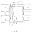
- FIG. 3 is a schematic top view of a power semiconductor package embodying this invention.
- FIG. 4 is a schematic top view to illustrate a metal sheet in an uncut state before forming the power semiconductor package of FIG. 3;
- FIG. 5 is a schematic cross-sectional side view of the power semiconductor package of FIG. 4 taken along line V—V to illustrate connection of a source terminal and a first contacting portion of the metal sheet;
- FIG. 6 is a schematic side view of the power semiconductor package of FIG. 4 taken along line VI—VI to illustrate connection of a gate terminal and a second contacting portion of the metal sheet.
- FIGS. 3, 5 and 6 illustrate a power semiconductor package embodying this invention.
- the power semiconductor package includes a power MOSFET die 41 , a first metal sheet 432 , a second metal sheet 431 , a plurality of aligned first terminals 422 , a plurality of aligned second terminals 423 , and a third terminal 424 .
- the power MOSFET die 41 has a bottom surface defining a drain contact (not shown), and a top surface which includes a first metallized region defining a source contact 411 , and a second metallized region defining a gate contact 412 .
- the first metal sheet 432 is coupled to and is electrically connected to the source contact 411 via a conductive material (not shown), such as a conductive paste or a conductive epoxy, and has one end extending outwardly from the power MOSFET die 41 .
- the second metal sheet 431 is coupled to and is electrically connected to the gate contact 412 via the conductive material (not shown), and has one end extending outwardly from the power MOSFET die 41 .
- the first terminals 422 are disposed adjacent to the power MOSFET die 41 , and are coupled to and are electrically connected to the drain contact via another conductive material (not shown), such as a conductive epoxy or a conductive paste that contains silver.
- the second terminals 423 are disposed adjacent to the power MOSFET die 41 , and respectively have substantially V-shaped end portions 4231 that respectively confine substantially V-shaped grooves 4232 to receive said one end of the first metal sheet 432 , and that are coupled to and are electrically connected to said one end of the first metal sheet 432 via the conductive material 441 .
- the third terminal 424 is disposed adjacent to the power MOSFET die 41 , and has a substantially V-shaped end portion 4241 that confines a substantially V-shaped groove 4242 to receive said one end of the second metal sheet 431 , and that is coupled to and electrically connected to said one end of the second metal sheet 431 via the conductive material 441 .
- the power semiconductor package of this invention is made by a method that comprises the steps of: providing the aforesaid power MOSFET die 41 , providing a lead frame 42 that includes the aforesaid first, second, and third terminals 422 , 423 , 424 , providing a metal sheet 43 that includes first and second contacting portions which define respectively the aforesaid first and second metal sheets 432 , 431 , and a bridging portion 433 which interconnects the first and second contacting portions, mounting the power MOSFET die 41 on the lead frame 42 such that the drain contact is coupled to and is electrically connected to the first terminal 422 via a conductive material (not shown), attaching the metal sheet 43 to the top surface of the power MOSFET die 41 and the second and third terminals 423 , 424 of the lead frame 42 such that the source contact 411 and the V-shaped end portions 4231 of the second terminals 423 are coupled to and are electrically
- the connections of the source contact 411 to the second terminals 423 and the gate contact 411 to the third terminal 424 in the production of the power semiconductor package of this invention can be accomplished simultaneously via a bonding apparatus, thereby eliminating the use of two bonding apparatuses and the contamination problem associated with the prior art.
- the designs of the V-shaped end portions 4231 of the second terminals 423 and the V-shaped end portions 4241 of the third terminal 423 are able to facilitate and to improve qualitatively the bonding of the metal sheet 43 to the source and gate terminals 423 , 424 .
Abstract
A power semiconductor die has a drain contact, a source contact, and a gate contact. A lead frame has first, second, and third terminals. A metal sheet has first and second contacting portions and a bridging portion interconnecting the first and second contacting portions. The power semiconductor die is mounted on the lead frame such that the drain contact is connected to the first terminal. The metal sheet is attached to the top surface of the power semiconductor die and the second and third terminals of the lead frame such that the source contact and the second terminal are connected to the first contacting portion, and such that the gate contact and the third terminal are connected to the second contacting portion. The bridging portion is subsequently cut for disconnecting electrically the first and second contacting portions.
Description
1. Field of the Invention
This invention relates to a power semiconductor package and a method for making the same, more particularly to a power semiconductor package with a power MOSFET die and a method for making the same.
2. Description of the Related Art
FIG. 1 illustrates a conventional power semiconductor package. The power semiconductor package includes a semiconductor die 11, such as a power MOSFET die, which has a bottom surface defining a drain contact (not shown), and a top surface that includes a first metallized region defining a source contact 111 and a second metallized region defining a gate contact 112. The power semiconductor package further includes a bottom metal plate 121 coupled to and electrically connected to the drain contact, a plurality of drain terminals 122 extending outwardly from the bottom metal plate 121 to be electrically connected to the drain contact, a plurality of spaced apart source terminals 123 electrically connected to the source contact 111 via a plurality of gold wires 125, and a gate terminal 124 electrically connected to the gate contact 112 via a gold wire 126.
The aforesaid power semiconductor package is disadvantageous in that in order to reduce the electrical resistance from the source contact 111 to the source terminals 123, a large number of the gold wires 125 are required to be employed in the power semiconductor package. Since the gold wires 125 are very expensive and can only be stitch bonded to the source contact 111 and the source terminal 123 one at a time, such number of the gold wires 125 will increase the production cost and the manufacturing time considerably. In addition, the reduction of the electrical resistance is still poor, due to a relatively small increase in the cross-sectional area of the gold wires 125 when a large number of the gold wires 125 is employed. Moreover, the gold wires 125 may not be able to provide sufficient surface area for dissipating a large amount of heat generated by the semiconductor die 11, particularly by a high current power MOSFET die, during operation.
FIG. 2 illustrates another conventional power semiconductor package that employs a metal plate 23 to replace the gold wires 125 so as to reduce the aforesaid electrical resistance and to increase the surface area as required to dissipate the aforementioned heat, and to reduce the manufacturing time due to elimination of the wire bonding operation for the gold wires 125. However, the power semiconductor package of this type is disadvantageous in that two bonding apparatuses are needed for stitch bonding the gold wire 126 to the gate contact 112 and the gate terminal 124 and for bonding the metal plate 23 to the source contact 111 and the source terminals 123 in the production of the power semiconductor package. Moreover, the size of the metal plate 23 employed in the power semiconductor package is preferably as large as possible to cover the source contact 111 without extending to the gate contact 112. However, the metal plate 23 is normally coupled to the source contact 111 via a conductive material, such as a conductive epoxy or a conductive paste, which can overflow and interfere with the surface of the gate contact 112 upon curing or reflowing of the conductive material. As a consequence, the gate contact 112 may be contaminated with the conductive material, and the gold wire 26 may be poorly stitch bonded to the gate contact 112 because of the aforesaid contamination.
Therefore, the object of the present invention is to provide a method for bonding a power semiconductor die to a lead frame via a metal sheet that is capable of overcoming the aforementioned problems.
Another object of the present invention is to provide a power semiconductor package that includes a power MOSFET die, a metal sheet coupled to a source contact on the power MOSFET die, and a terminal having a V-shaped end portion which is able to facilitate connection of the terminal to the metal sheet.
According to one aspect of the present invention, a method for bonding a power semiconductor die to a lead frame comprises the steps of: providing a power semiconductor die that has a bottom surface defining a drain contact, and a top surface which includes a first metallized region defining a source contact, and a second metallized region defining a gate contact; providing a lead frame that has first, second, and third terminals; providing a metal sheet that has first and second contacting portions and a bridging portion interconnecting the first and second contacting portions; mounting the power semiconductor die on the lead frame such that the drain contact is coupled to and is electrically connected to the first terminal; attaching the metal sheet to the top surface of the power semiconductor die and the second and third terminals of the lead frame such that the source contact and the second terminal are coupled to and are electrically connected to the first contacting portion, and such that the gate contact and the third terminal are coupled to and are electrically connected to the second contacting portion; and cutting the bridging portion for disconnecting electrically the first and second contacting portions.
According to another aspect of the present invention, a power semiconductor package comprises: a power MOSFET die that has a bottom surface defining a drain contact, and a top surface which includes a first metallized region defining a source contact, and a second metallized region defining a gate contact; a first metal sheet that is coupled to and that is electrically connected to the source contact, and that has one end extending outwardly from the power MOSFET die; a second metal sheet that is coupled to and that is electrically connected to the gate contact; a first terminal disposed adjacent to the power MOSFET die and coupled to and electrically connected to the drain contact; a second terminal disposed adjacent to the power MOSFET die and having a substantially V-shaped end portion that confines a substantially V-shaped groove to receive said one end of the first metal sheet, the V-shaped end portion of the second terminal being coupled to and being electrically connected to said one end of the first metal sheet; and a third terminal disposed adjacent to the power MOSFET die and coupled to and electrically connected to the second metal sheet.
In drawings which illustrate an embodiment of the invention,
FIG. 1 is a schematic top view of a conventional power semiconductor package;
FIG. 2 is schematic top view of another conventional power semiconductor package;
FIG. 3 is a schematic top view of a power semiconductor package embodying this invention;
FIG. 4 is a schematic top view to illustrate a metal sheet in an uncut state before forming the power semiconductor package of FIG. 3;
FIG. 5 is a schematic cross-sectional side view of the power semiconductor package of FIG. 4 taken along line V—V to illustrate connection of a source terminal and a first contacting portion of the metal sheet; and
FIG. 6 is a schematic side view of the power semiconductor package of FIG. 4 taken along line VI—VI to illustrate connection of a gate terminal and a second contacting portion of the metal sheet.
FIGS. 3, 5 and 6 illustrate a power semiconductor package embodying this invention. The power semiconductor package includes a power MOSFET die 41, a first metal sheet 432, a second metal sheet 431, a plurality of aligned first terminals 422, a plurality of aligned second terminals 423, and a third terminal 424. The power MOSFET die 41 has a bottom surface defining a drain contact (not shown), and a top surface which includes a first metallized region defining a source contact 411, and a second metallized region defining a gate contact 412. The first metal sheet 432 is coupled to and is electrically connected to the source contact 411 via a conductive material (not shown), such as a conductive paste or a conductive epoxy, and has one end extending outwardly from the power MOSFET die 41. The second metal sheet 431 is coupled to and is electrically connected to the gate contact 412 via the conductive material (not shown), and has one end extending outwardly from the power MOSFET die 41. The first terminals 422 are disposed adjacent to the power MOSFET die 41, and are coupled to and are electrically connected to the drain contact via another conductive material (not shown), such as a conductive epoxy or a conductive paste that contains silver. The second terminals 423 are disposed adjacent to the power MOSFET die 41, and respectively have substantially V-shaped end portions 4231 that respectively confine substantially V-shaped grooves 4232 to receive said one end of the first metal sheet 432, and that are coupled to and are electrically connected to said one end of the first metal sheet 432 via the conductive material 441. The third terminal 424 is disposed adjacent to the power MOSFET die 41, and has a substantially V-shaped end portion 4241 that confines a substantially V-shaped groove 4242 to receive said one end of the second metal sheet 431, and that is coupled to and electrically connected to said one end of the second metal sheet 431 via the conductive material 441.
Referring now to FIG. 4, in combination with FIGS. 3, 5 and 6, the power semiconductor package of this invention is made by a method that comprises the steps of: providing the aforesaid power MOSFET die 41, providing a lead frame 42 that includes the aforesaid first, second, and third terminals 422, 423, 424, providing a metal sheet 43 that includes first and second contacting portions which define respectively the aforesaid first and second metal sheets 432, 431, and a bridging portion 433 which interconnects the first and second contacting portions, mounting the power MOSFET die 41 on the lead frame 42 such that the drain contact is coupled to and is electrically connected to the first terminal 422 via a conductive material (not shown), attaching the metal sheet 43 to the top surface of the power MOSFET die 41 and the second and third terminals 423, 424 of the lead frame 42 such that the source contact 411 and the V-shaped end portions 4231 of the second terminals 423 are coupled to and are electrically connected to the first contacting portion of the metal sheet 43 via the conductive material 411, and such that the gate contact 412 and the V-shaped end portion 4241 of the third terminal 424 are coupled to and are electrically connected to the second contacting portion of the metal sheet 43 via the conductive material 411, and cutting the bridging portion 433 for disconnecting electrically the first and second contacting portions of the metal sheet 43 via a cutter (not shown), such as a laser cutter.
With the metal sheet 43 as a bonding medium, the connections of the source contact 411 to the second terminals 423 and the gate contact 411 to the third terminal 424 in the production of the power semiconductor package of this invention can be accomplished simultaneously via a bonding apparatus, thereby eliminating the use of two bonding apparatuses and the contamination problem associated with the prior art. Moreover, the designs of the V-shaped end portions 4231 of the second terminals 423 and the V-shaped end portions 4241 of the third terminal 423 are able to facilitate and to improve qualitatively the bonding of the metal sheet 43 to the source and gate terminals 423, 424.
With the invention thus explained, it is apparent that various modifications and variations can be made without departing from the spirit of the present invention. It is therefore intended that the invention be limited only as recited in the appended claims.
Claims (3)
1. A method for bonding a power semiconductor die to a lead frame, comprising the steps of:
providing a power semiconductor die that has a bottom surface defining a drain contact, and a top surface which includes a first metallized region defining a source contact, and a second metallized region defining a gate contact;
providing a lead frame that has first, second, and third terminals;
providing a metal sheet that has first and second contacting portions and a bridging portion interconnecting the first and second contacting portions;
mounting the power semiconductor die on the lead frame such that the drain contact is coupled to and is electrically connected to the first terminal;
attaching the metal sheet to the top surface of the power semiconductor die and the second and third terminals of the lead frame such that the source contact and the second terminal are coupled to and are electrically connected to the first contacting portion, and such that the gate contact and the third terminal are coupled to and are electrically connected to the second contacting portion; and
cutting the bridging portion for disconnecting electrically the first and second contacting portions.
2. The method of claim 1 , wherein the first and second contacting portions and the bridging portion of the metal sheet are integrally formed.
3. The method of claim 1 , wherein the power semiconductor die is a MOSFET die.
Applications Claiming Priority (2)
| Application Number | Priority Date | Filing Date | Title |
|---|---|---|---|
| TW089109555A TW451392B (en) | 2000-05-18 | 2000-05-18 | Leadframe connecting method of power transistor |
| TW089109555 | 2000-05-18 |
Publications (2)
| Publication Number | Publication Date |
|---|---|
| US20010044167A1 US20010044167A1 (en) | 2001-11-22 |
| US6465276B2 true US6465276B2 (en) | 2002-10-15 |
Family
ID=21659773
Family Applications (1)
| Application Number | Title | Priority Date | Filing Date |
|---|---|---|---|
| US09/879,367 Expired - Lifetime US6465276B2 (en) | 2000-05-18 | 2001-06-12 | Power semiconductor package and method for making the same |
Country Status (2)
| Country | Link |
|---|---|
| US (1) | US6465276B2 (en) |
| TW (1) | TW451392B (en) |
Cited By (18)
| Publication number | Priority date | Publication date | Assignee | Title |
|---|---|---|---|---|
| US20050130350A1 (en) * | 2000-04-13 | 2005-06-16 | Estacio Maria Cristina B. | Flip clip attach and copper clip attach on MOSFET device |
| US20050212101A1 (en) * | 2001-04-18 | 2005-09-29 | Norihide Funato | Semiconductor device and method of manufacturing the same |
| US20060145319A1 (en) * | 2004-12-31 | 2006-07-06 | Ming Sun | Flip chip contact (FCC) power package |
| US20060226498A1 (en) * | 2005-01-06 | 2006-10-12 | Hvvi Semiconductors,Inc. | Power semiconductor device and method therefor |
| US20060226451A1 (en) * | 2004-01-10 | 2006-10-12 | Hvvi Semiconductors, Inc. | Power semiconductor device and method therefor |
| US20060252253A1 (en) * | 2003-02-28 | 2006-11-09 | Norbert Seliger | Internal connection system for power semiconductors comprising large-area terminals |
| US20070114352A1 (en) * | 2005-11-18 | 2007-05-24 | Victor R Cruz Erwin | Semiconductor die package using leadframe and clip and method of manufacturing |
| DE102005057401A1 (en) * | 2005-11-30 | 2007-05-31 | Infineon Technologies Ag | Semiconductor component and production process for power uses has semiconductor element with chip island having two contact strips in separate planes above the semiconductor element |
| US20070155058A1 (en) * | 2006-01-05 | 2007-07-05 | Jereza Armand Vincent C | Clipless and wireless semiconductor die package and method for making the same |
| US20080173991A1 (en) * | 2007-01-24 | 2008-07-24 | Erwin Victor Cruz | Pre-molded clip structure |
| US20090091010A1 (en) * | 2007-10-09 | 2009-04-09 | Paul Armand Calo | Wireless semiconductor package for efficient heat dissipation |
| US20090160036A1 (en) * | 2007-12-19 | 2009-06-25 | David Grey | Package with multiple dies |
| US20090179313A1 (en) * | 2008-01-10 | 2009-07-16 | Maria Clemens Quinones | Flex clip connector for semiconductor device |
| US20090294934A1 (en) * | 2008-05-30 | 2009-12-03 | Alpha & Omega Semiconductor, Ltd. | Conductive clip for semiconductor device package |
| US20100164078A1 (en) * | 2008-12-31 | 2010-07-01 | Ruben Madrid | Package assembly for semiconductor devices |
| US7843048B2 (en) | 2008-05-05 | 2010-11-30 | Fairchild Semiconductor Corporation | Multi-chip discrete devices in semiconductor packages |
| DE102015103555A1 (en) * | 2014-03-19 | 2015-10-08 | Infineon Technologies Austria Ag | Electronic component and leadframe |
| US11444010B2 (en) * | 2019-10-21 | 2022-09-13 | Renesas Electronics Corporation | Semiconductor device |
Families Citing this family (13)
| Publication number | Priority date | Publication date | Assignee | Title |
|---|---|---|---|---|
| US6593527B1 (en) * | 2002-04-17 | 2003-07-15 | Delphi Technologies, Inc. | Integrated circuit assembly with bar bond attachment |
| DE10301091B4 (en) * | 2003-01-14 | 2015-01-22 | Infineon Technologies Ag | Power semiconductor device and method for connecting semiconductor devices associated with a common substrate carrier |
| DE10303463B4 (en) * | 2003-01-29 | 2006-06-14 | Infineon Technologies Ag | Semiconductor device having at least two integrated in a housing and contacted by a common contact clip chips |
| DE102004041088B4 (en) * | 2004-08-24 | 2009-07-02 | Infineon Technologies Ag | Semiconductor component in flat conductor technology with a semiconductor chip and method for its production |
| JP2007165714A (en) * | 2005-12-15 | 2007-06-28 | Renesas Technology Corp | Semiconductor device |
| FR2901408A1 (en) * | 2006-09-27 | 2007-11-23 | Siemens Vdo Automotive Sas | Conductive substrate e.g. lead frame, and electronic component e.g. power module, connecting device, has conductive substrate circulating high power currents and including thin part i.e. tongue, formed in substrate in form of loop |
| US8299394B2 (en) * | 2007-06-15 | 2012-10-30 | Sv Probe Pte Ltd. | Approach for assembling and repairing probe assemblies using laser welding |
| US7902657B2 (en) * | 2007-08-28 | 2011-03-08 | Fairchild Semiconductor Corporation | Self locking and aligning clip structure for semiconductor die package |
| JP4865829B2 (en) * | 2009-03-31 | 2012-02-01 | シャープ株式会社 | Semiconductor device and manufacturing method thereof |
| DE102012019391A1 (en) * | 2012-10-02 | 2014-04-03 | Infineon Technologies Ag | Conductive semiconductor housing with redundant functionality |
| KR102123263B1 (en) * | 2016-01-07 | 2020-06-16 | 주식회사 쏠리드 | Communication module assembly |
| CN112259516A (en) * | 2019-07-22 | 2021-01-22 | 无锡华润华晶微电子有限公司 | Semiconductor packaging structure |
| CN116072647B (en) * | 2023-03-28 | 2023-07-18 | 深圳市深鸿盛电子有限公司 | MOS chip packaging structure and packaging method thereof |
Citations (6)
| Publication number | Priority date | Publication date | Assignee | Title |
|---|---|---|---|---|
| US5105536A (en) * | 1989-07-03 | 1992-04-21 | General Electric Company | Method of packaging a semiconductor chip in a low inductance package |
| US5637922A (en) * | 1994-02-07 | 1997-06-10 | General Electric Company | Wireless radio frequency power semiconductor devices using high density interconnect |
| US6040626A (en) * | 1998-09-25 | 2000-03-21 | International Rectifier Corp. | Semiconductor package |
| US6165820A (en) * | 1994-12-22 | 2000-12-26 | Pace; Benedict G. | Package for electronic devices |
| US6307755B1 (en) * | 1999-05-27 | 2001-10-23 | Richard K. Williams | Surface mount semiconductor package, die-leadframe combination and leadframe therefor and method of mounting leadframes to surfaces of semiconductor die |
| US6319755B1 (en) * | 1999-12-01 | 2001-11-20 | Amkor Technology, Inc. | Conductive strap attachment process that allows electrical connector between an integrated circuit die and leadframe |
-
2000
- 2000-05-18 TW TW089109555A patent/TW451392B/en not_active IP Right Cessation
-
2001
- 2001-06-12 US US09/879,367 patent/US6465276B2/en not_active Expired - Lifetime
Patent Citations (6)
| Publication number | Priority date | Publication date | Assignee | Title |
|---|---|---|---|---|
| US5105536A (en) * | 1989-07-03 | 1992-04-21 | General Electric Company | Method of packaging a semiconductor chip in a low inductance package |
| US5637922A (en) * | 1994-02-07 | 1997-06-10 | General Electric Company | Wireless radio frequency power semiconductor devices using high density interconnect |
| US6165820A (en) * | 1994-12-22 | 2000-12-26 | Pace; Benedict G. | Package for electronic devices |
| US6040626A (en) * | 1998-09-25 | 2000-03-21 | International Rectifier Corp. | Semiconductor package |
| US6307755B1 (en) * | 1999-05-27 | 2001-10-23 | Richard K. Williams | Surface mount semiconductor package, die-leadframe combination and leadframe therefor and method of mounting leadframes to surfaces of semiconductor die |
| US6319755B1 (en) * | 1999-12-01 | 2001-11-20 | Amkor Technology, Inc. | Conductive strap attachment process that allows electrical connector between an integrated circuit die and leadframe |
Cited By (55)
| Publication number | Priority date | Publication date | Assignee | Title |
|---|---|---|---|---|
| US7052938B2 (en) | 2000-04-13 | 2006-05-30 | Fairchild Semiconductor Corporation | Flip clip attach and copper clip attach on MOSFET device |
| US20050130350A1 (en) * | 2000-04-13 | 2005-06-16 | Estacio Maria Cristina B. | Flip clip attach and copper clip attach on MOSFET device |
| US20070052075A1 (en) * | 2001-04-18 | 2007-03-08 | Norihide Funato | Semiconductor device and method of manufacturing the same |
| US20050212101A1 (en) * | 2001-04-18 | 2005-09-29 | Norihide Funato | Semiconductor device and method of manufacturing the same |
| US7364950B2 (en) | 2001-04-18 | 2008-04-29 | Kabushiki Kaisha Toshiba | Semiconductor device and method of manufacturing the same |
| US7230322B2 (en) * | 2001-04-18 | 2007-06-12 | Kabushiki Kaisha Toshiba | Semiconductor device and method of manufacturing the same |
| US20060252253A1 (en) * | 2003-02-28 | 2006-11-09 | Norbert Seliger | Internal connection system for power semiconductors comprising large-area terminals |
| US7427532B2 (en) | 2003-02-28 | 2008-09-23 | Siemens Aktiengesellschaft | Method of manufacturing a device having a contacting structure |
| US8471378B2 (en) | 2004-01-10 | 2013-06-25 | Estivation Properties Llc | Power semiconductor device and method therefor |
| US20100032750A1 (en) * | 2004-01-10 | 2010-02-11 | Hvvi Semiconductors, Inc. | Power Semiconductor Device And Method Therefor |
| US9865590B2 (en) | 2004-01-10 | 2018-01-09 | Xenogenic Development Limited Liability Company | Power semiconductor device and method therefor |
| US20060226451A1 (en) * | 2004-01-10 | 2006-10-12 | Hvvi Semiconductors, Inc. | Power semiconductor device and method therefor |
| US9177866B2 (en) | 2004-01-10 | 2015-11-03 | Estivation Properties Llc | Power semiconductor device and method therefor |
| US7847369B2 (en) | 2004-01-10 | 2010-12-07 | Hvvi Semiconductors, Inc. | Radio frequency power semiconductor device comprising matrix of cavities as dielectric isolation structure |
| US7898057B2 (en) | 2004-01-10 | 2011-03-01 | Hvvi Semiconductors, Inc. | Radio frequency power semiconductor device package comprising dielectric platform and shielding plate |
| US20070090434A1 (en) * | 2004-01-10 | 2007-04-26 | Hvvi Semiconductors, Inc. | Power semiconductor device and method therefor |
| US9029946B2 (en) | 2004-01-10 | 2015-05-12 | Estivation Properties Llc | Power semiconductor device and method therefor |
| US20060145319A1 (en) * | 2004-12-31 | 2006-07-06 | Ming Sun | Flip chip contact (FCC) power package |
| US8530963B2 (en) | 2005-01-06 | 2013-09-10 | Estivation Properties Llc | Power semiconductor device and method therefor |
| US20060226498A1 (en) * | 2005-01-06 | 2006-10-12 | Hvvi Semiconductors,Inc. | Power semiconductor device and method therefor |
| US20080044946A1 (en) * | 2005-11-18 | 2008-02-21 | Cruz Erwin Victor R | Semiconductor die package using leadframe and clip and method of manufacturing |
| US8058107B2 (en) | 2005-11-18 | 2011-11-15 | Cruz Erwin Victor R | Semiconductor die package using leadframe and clip and method of manufacturing |
| US7285849B2 (en) | 2005-11-18 | 2007-10-23 | Fairchild Semiconductor Corporation | Semiconductor die package using leadframe and clip and method of manufacturing |
| US20070114352A1 (en) * | 2005-11-18 | 2007-05-24 | Victor R Cruz Erwin | Semiconductor die package using leadframe and clip and method of manufacturing |
| US20070145573A1 (en) * | 2005-11-30 | 2007-06-28 | Ralf Otremba | Semiconductor Device And Method For Producing The Same |
| US7745929B2 (en) | 2005-11-30 | 2010-06-29 | Infineon Technologies Ag | Semiconductor device and method for producing the same |
| DE102005057401B4 (en) * | 2005-11-30 | 2009-10-08 | Infineon Technologies Ag | Semiconductor component and method for its production |
| DE102005057401A1 (en) * | 2005-11-30 | 2007-05-31 | Infineon Technologies Ag | Semiconductor component and production process for power uses has semiconductor element with chip island having two contact strips in separate planes above the semiconductor element |
| US20070155058A1 (en) * | 2006-01-05 | 2007-07-05 | Jereza Armand Vincent C | Clipless and wireless semiconductor die package and method for making the same |
| US7371616B2 (en) | 2006-01-05 | 2008-05-13 | Fairchild Semiconductor Corporation | Clipless and wireless semiconductor die package and method for making the same |
| US7768105B2 (en) | 2007-01-24 | 2010-08-03 | Fairchild Semiconductor Corporation | Pre-molded clip structure |
| US20080173991A1 (en) * | 2007-01-24 | 2008-07-24 | Erwin Victor Cruz | Pre-molded clip structure |
| US8513059B2 (en) * | 2007-01-24 | 2013-08-20 | Fairchild Semiconductor Corporation | Pre-molded clip structure |
| US20110272794A1 (en) * | 2007-01-24 | 2011-11-10 | Erwin Victor Cruz | Pre-molded clip structure |
| WO2008091742A2 (en) * | 2007-01-24 | 2008-07-31 | Fairchild Semiconductor Corporation | Pre-molded clip structure |
| US20100258924A1 (en) * | 2007-01-24 | 2010-10-14 | Erwin Victor Cruz | Pre-molded clip structure |
| CN101595560B (en) * | 2007-01-24 | 2012-07-04 | 费查尔德半导体有限公司 | Pre-molded clip structure |
| US7838340B2 (en) | 2007-01-24 | 2010-11-23 | Fairchild Semiconductor Corporation | Pre-molded clip structure |
| WO2008091742A3 (en) * | 2007-01-24 | 2008-11-20 | Fairchild Semiconductor | Pre-molded clip structure |
| US8008759B2 (en) * | 2007-01-24 | 2011-08-30 | Fairchild Semiconductor Corporation | Pre-molded clip structure |
| US7586179B2 (en) | 2007-10-09 | 2009-09-08 | Fairchild Semiconductor Corporation | Wireless semiconductor package for efficient heat dissipation |
| US20090091010A1 (en) * | 2007-10-09 | 2009-04-09 | Paul Armand Calo | Wireless semiconductor package for efficient heat dissipation |
| US20090160036A1 (en) * | 2007-12-19 | 2009-06-25 | David Grey | Package with multiple dies |
| US7781872B2 (en) | 2007-12-19 | 2010-08-24 | Fairchild Semiconductor Corporation | Package with multiple dies |
| US7824966B2 (en) | 2008-01-10 | 2010-11-02 | Fairchild Semiconductor Corporation | Flex chip connector for semiconductor device |
| US20090179313A1 (en) * | 2008-01-10 | 2009-07-16 | Maria Clemens Quinones | Flex clip connector for semiconductor device |
| US20090311832A1 (en) * | 2008-01-10 | 2009-12-17 | Quinones Maria Clemens Y | Flex Chip Connector For Semiconductor Device |
| US7626249B2 (en) | 2008-01-10 | 2009-12-01 | Fairchild Semiconductor Corporation | Flex clip connector for semiconductor device |
| US7843048B2 (en) | 2008-05-05 | 2010-11-30 | Fairchild Semiconductor Corporation | Multi-chip discrete devices in semiconductor packages |
| US8680658B2 (en) | 2008-05-30 | 2014-03-25 | Alpha And Omega Semiconductor Incorporated | Conductive clip for semiconductor device package |
| US20090294934A1 (en) * | 2008-05-30 | 2009-12-03 | Alpha & Omega Semiconductor, Ltd. | Conductive clip for semiconductor device package |
| US20100164078A1 (en) * | 2008-12-31 | 2010-07-01 | Ruben Madrid | Package assembly for semiconductor devices |
| DE102015103555A1 (en) * | 2014-03-19 | 2015-10-08 | Infineon Technologies Austria Ag | Electronic component and leadframe |
| DE102015103555B4 (en) | 2014-03-19 | 2022-03-24 | Infineon Technologies Austria Ag | electronic component |
| US11444010B2 (en) * | 2019-10-21 | 2022-09-13 | Renesas Electronics Corporation | Semiconductor device |
Also Published As
| Publication number | Publication date |
|---|---|
| TW451392B (en) | 2001-08-21 |
| US20010044167A1 (en) | 2001-11-22 |
Similar Documents
| Publication | Publication Date | Title |
|---|---|---|
| US6465276B2 (en) | Power semiconductor package and method for making the same | |
| US7906375B2 (en) | Compact co-packaged semiconductor dies with elevation-adaptive interconnection plates | |
| EP3226292B1 (en) | Lead frame, semiconductor device, method for manufacturing lead frame, and method for manufacturing semiconductor device | |
| US7449774B1 (en) | Semiconductor power module having an electrically insulating heat sink and method of manufacturing the same | |
| US8324726B2 (en) | Semiconductor device, electrode member and electrode member fabrication method | |
| EP2306513A2 (en) | IC chip package with directly connected leads | |
| JP3146452B2 (en) | Surface mount type LED element and method of manufacturing the same | |
| US6794736B1 (en) | Semiconductor device | |
| US9433075B2 (en) | Electric power semiconductor device | |
| CN104485321A (en) | Semiconductor die package and method for making the same | |
| US10586755B2 (en) | Semiconductor device, and method for manufacturing semiconductor device | |
| US8569871B2 (en) | Semiconductor device having a molded package | |
| US11742279B2 (en) | Semiconductor device | |
| JP4100332B2 (en) | Electronic device and manufacturing method thereof | |
| US6593527B1 (en) | Integrated circuit assembly with bar bond attachment | |
| JPH11191561A (en) | Manufacture of semiconductor device | |
| US5324890A (en) | Direct bond copper-output footprint | |
| JP2006310609A (en) | Semiconductor device | |
| EP1271648A1 (en) | Power semiconductor package and method for making the same | |
| JP2968198B2 (en) | Surface mount type semiconductor package | |
| US6441472B1 (en) | Semiconductor device and method of manufacturing the same | |
| CN112635411A (en) | Semiconductor package with top or bottom side cooling | |
| JP2005051109A (en) | Power semiconductor module | |
| CN111192860A (en) | Gallium nitride device and packaging method thereof | |
| WO2021220357A1 (en) | Semiconductor device |
Legal Events
| Date | Code | Title | Description |
|---|---|---|---|
| AS | Assignment |
Owner name: SILICONX (TAIWAN) LTD., TAIWAN Free format text: ASSIGNMENT OF ASSIGNORS INTEREST;ASSIGNOR:KUO, FRANK;REEL/FRAME:011900/0556 Effective date: 20010514 |
|
| STCF | Information on status: patent grant |
Free format text: PATENTED CASE |
|
| FPAY | Fee payment |
Year of fee payment: 4 |
|
| FPAY | Fee payment |
Year of fee payment: 8 |
|
| FPAY | Fee payment |
Year of fee payment: 12 |