US6471526B1 - Electrical connector with strain relief feature - Google Patents
Electrical connector with strain relief feature Download PDFInfo
- Publication number
- US6471526B1 US6471526B1 US09/465,164 US46516499A US6471526B1 US 6471526 B1 US6471526 B1 US 6471526B1 US 46516499 A US46516499 A US 46516499A US 6471526 B1 US6471526 B1 US 6471526B1
- Authority
- US
- United States
- Prior art keywords
- contacts
- group
- substrate
- connector
- bodies
- Prior art date
- Legal status (The legal status is an assumption and is not a legal conclusion. Google has not performed a legal analysis and makes no representation as to the accuracy of the status listed.)
- Expired - Lifetime
Links
- 239000000758 substrate Substances 0.000 claims abstract description 61
- 239000004020 conductor Substances 0.000 claims abstract description 20
- 239000011159 matrix material Substances 0.000 claims description 17
- 230000002093 peripheral effect Effects 0.000 claims description 3
- 229910000679 solder Inorganic materials 0.000 description 58
- 238000001514 detection method Methods 0.000 description 12
- 230000013011 mating Effects 0.000 description 9
- 238000000034 method Methods 0.000 description 8
- 238000013459 approach Methods 0.000 description 5
- 230000011664 signaling Effects 0.000 description 3
- 239000003351 stiffener Substances 0.000 description 3
- 229920000106 Liquid crystal polymer Polymers 0.000 description 2
- 239000004977 Liquid-crystal polymers (LCPs) Substances 0.000 description 2
- 238000010586 diagram Methods 0.000 description 2
- 238000005516 engineering process Methods 0.000 description 2
- 238000004519 manufacturing process Methods 0.000 description 2
- 238000012986 modification Methods 0.000 description 2
- 230000004048 modification Effects 0.000 description 2
- 229920002799 BoPET Polymers 0.000 description 1
- 239000005041 Mylar™ Substances 0.000 description 1
- 239000004642 Polyimide Substances 0.000 description 1
- 238000004891 communication Methods 0.000 description 1
- 230000003247 decreasing effect Effects 0.000 description 1
- 239000012634 fragment Substances 0.000 description 1
- 239000004033 plastic Substances 0.000 description 1
- 229920003223 poly(pyromellitimide-1,4-diphenyl ether) Polymers 0.000 description 1
- 229920006267 polyester film Polymers 0.000 description 1
- 229920001721 polyimide Polymers 0.000 description 1
- 239000007787 solid Substances 0.000 description 1
Images


Classifications
-
- H—ELECTRICITY
- H05—ELECTRIC TECHNIQUES NOT OTHERWISE PROVIDED FOR
- H05K—PRINTED CIRCUITS; CASINGS OR CONSTRUCTIONAL DETAILS OF ELECTRIC APPARATUS; MANUFACTURE OF ASSEMBLAGES OF ELECTRICAL COMPONENTS
- H05K7/00—Constructional details common to different types of electric apparatus
- H05K7/02—Arrangements of circuit components or wiring on supporting structure
- H05K7/10—Plug-in assemblages of components, e.g. IC sockets
- H05K7/1053—Plug-in assemblages of components, e.g. IC sockets having interior leads
- H05K7/1061—Plug-in assemblages of components, e.g. IC sockets having interior leads co-operating by abutting
Definitions
- the present invention relates to an electrical connector. More specifically, the present invention relates to high input/output density connectors, such as surface mount connectors using ball grid array (BGA) technology.
- BGA ball grid array
- BGA connectors have become a reliable and efficient technique for mounting high density electrical connectors on substrates using SMT.
- BGA connectors have an insulative connector housing. One side of the connector housing has a matrix of spherical solder balls, positioned to engage the conductive paths of a circuit substrate. The opposite side of the connector housing has a corresponding matrix of contact terminals, which extend through the connector housing and connect electrically to the solder balls. These contact terminals are designed to engage another BGA connector, similarly connected to another substrate, thus permitting board-to-board interconnection.
- BGA connectors may be used to interconnect a number of various types of circuit substrates, including flexible circuits.
- a flexible circuit is a pliable electrical conductor device in which conductive tracings are photolithographed on a base sheet of polyimide or polyester film, such as manufactured and sold by E. I. du Pont de Nemours & Co. under the trademarks “Kapton” (U.S. Pat. No. 3,781,596) or “Mylar.” Because of their light weight and ability to bend and adapt to confined locations, flexible circuits are used in a variety of applications, including portable computers and portable communication devices. In addition, because of their ability to flex resiliently, flexible circuits are used on moving devices, like hard disk drives and compact disk pick-ups. Flexible circuits may be interconnected either to conventional circuit board substrates or to other flexible circuit substrates.
- the BGA connector has overcome the problem associated with low terminal density. As a result, the BGA connector has been used in flexible circuit applications. However, because of the dynamic environment of a flexible circuit, the BGA connector was also used in conjunction with a stiffener to be able to withstand the significant mechanical forces between it and the flexible substrate. Notably, these mechanical forces may be of concern when using BGA connectors to interconnect non-flexible circuit substrates as well.
- a first body of reflowable, electrically conductive material is placed on a contact, in order to provide an electrical path between the connector and the substrate.
- a second body of reflowable, electrically conductive material is placed on another contact. This second body provides mechanical strain relief between the connector and the substrate.
- the contacts of the electrical connector may be arranged in a matrix array.
- the second body may be disposed on adjacent contacts forming one or more rows or columns in the array.
- the second body may be disposed on adjacent contacts located in one or more corners of the array.
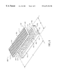
- FIG. 1 is a perspective view of one embodiment of the present invention in which a plurality of contacts form a matrix array
- FIG. 2 is a perspective view of the embodiment depicted in FIG. 1 in a mated, closed condition
- FIG. 3 is a side view of the embodiment depicted in FIG. 2;
- FIG. 4 is a side cross-sectional view in fragment of the alternative embodiment
- FIG. 5 is a plan view of a preferred embodiment according to the invention.
- FIG. 6 is a plan view of another preferred embodiment according to the invention.
- FIG. 7 is a plan view of another preferred embodiment according to the invention.
- FIG. 8 is a plan view of another preferred embodiment according to the invention.
- FIG. 9 is a block diagram of a detection device coupled to at least one contact in a preferred embodiment.
- the present invention is a board-to-board electrical connector system, wherein an electrical connector is attached to a corresponding board by a plurality of solder balls, some of which provide mechanical strain relief to the connector system.
- FIGS. 1-3 show various views of one embodiment of the invention.
- An electrical connector 100 includes a plug 104 and a receptacle 103 ; Plug 104 and receptacle 103 are removably engageable.
- Plug 104 and receptacle 103 each may have generally planar insulative housings 105 and 106 , respectively. These housings. 105 , 106 are preferably manufactured from an electrically non-conductive plastic, such as liquid crystal polymer (LCP).
- Plug 104 has a first edge 115 , a second edge 117 , a first side 111 , and a second side 113 .
- receptacle 103 has a first edge 116 , a second edge 118 , a first side 112 , and a second side 114 .
- Connector 100 has an overall length l and an overall width w.
- Receptacle 103 and plug 104 typically have a peripheral wall to protect the contacts and to provide rough alignment of receptacle 103 and plug 104 during mating.
- Connector 100 preferably interconnects two substrates 301 , 302 (as shown in FIG. 3 ), such as flexible printed circuit boards.
- Housing 105 has a mounting end 107 facing substrate 301 and a mating end 108 facing receptacle 103 .
- receptacle 103 has a housing 106 that has a mounting end 110 facing substrate 302 and a mating end 109 facing plug 104 .
- a plurality of contacts 102 extend generally perpendicular from mating end 109 of receptacle 103 .
- a plurality of contacts 401 extend generally perpendicular from mating end 108 of plug 104 .
- Contacts 102 which mate with contacts 401 may be any one of a number of different types, including blade-type and round pin contacts.
- contacts 102 , 401 may include several different types of contacts in a single plug or receptacle.
- Plurality of contacts 102 on receptacle 103 extend through housing 106 from mating end 109 to mounting end 110 . Fusible elements, such as solder balls 303 , attach to contacts 102 on mounting end 110 of housing 106 .
- plurality of contacts 401 (shown in FIG. 4) extend through housing 105 from mating end 108 to mounting end 107 . Fusible elements, such as solder balls 101 , attach to contacts 401 on mounting end 107 of housing 105 .
- contacts 102 , 401 form a matrix array of contacts, as shown in FIGS. 1 and 2. Consequently, solder balls 101 , 303 also preferably form a matrix array.
- a column refers to a group of solder balls 101 , 303 that extend along length l of connector 100 .
- a row refers to a group of solder balls 101 , 303 that extend along width w of connector 100 .
- plug 104 mounts to substrate 301 via solder balls 101 , preferably with present reflow techniques used in Ball Grid Array (BGA) technology.
- receptacle 103 mounts to substrate 302 via solder balls 303 . Because contacts 102 and 401 are electrically connected to solder balls 303 and 101 , respectively, when connector 100 is in a closed, mated position (as shown in FIGS. 2 - 4 ), substrate 301 is electrically interconnected to substrate 302 .
- substrates 301 and 302 are flexible circuit substrates.
- contacts 102 reside within apertures 404 of housing 106 .
- Contacts 102 are held within apertures 404 by interference fit and extend generally perpendicular to mating end 108 of housing 105 .
- contacts 401 reside within apertures 403 of housing 105 , and are held within apertures 403 by interference fit.
- Contacts 401 extend generally perpendicular to mating end 109 of housing 106 .
- Contacts 102 and contacts 401 have tail portions 405 and 406 , respectively. Tail portions 405 and 406 extend into recesses 415 and 416 , respectively.
- Tail portions 405 and 406 provide an electrical connection point for solder balls 301 and 101 , respectively, which may be placed in recesses 414 and 415 of housings 105 and 106 , respectively.
- PCT Application No. PCT/US97/18066 filed Oct. 7, 1997, entitled High Density Connector and Method of Manufacture, discloses methods of securing a solder ball to a contact and of securing a solder ball to a substrate.
- Contacts 102 also have upper arms 407 and 411 , flexibly connected to tail portions 405 of contacts 102 .
- Upper arms 407 and 411 have a converging section 412 and an outwardly diverging lead-in section 413 .
- As plug 104 and receptacle 103 mate upper portions 408 of contacts 401 flexibly engage upper arms 407 and 411 of contacts 102 .
- Recess 416 permits upper arms 407 and 411 to outwardly flex and accept upper portions 408 of contacts 401 into outwardly diverging lead-in section 413 .
- contacts 102 are electrically connected to contacts 401 , and thus solder balls 303 are electrically connected to solder balls 101 .
- contacts 401 as blade-type contacts and contacts 102 as scissor-type contacts, it should be appreciated that they may be any one of a number of different type contacts, including round pin contacts.
- contacts 102 , 401 may include several different types of contacts in a single plug or receptacle.
- Solder balls 101 and 303 may provide a variety of electrical functions, including carrying a signal, ground or power. In the present invention certain of solder balls 101 and 303 have been added to provide mechanical strain relief to the connection between substrates 301 , 302 and connector 100 , at the same time the remainder of solder balls 101 and 303 function to provide electrical interconnection.
- solder balls 101 , 303 are attached to substrates 301 , 302 that are flexible circuits. This is so because flexible circuits are bendable, and thus are used in applications where high mechanic strain is often induced on the connection between substrates 301 , 302 and solder balls 101 , 303 .
- the amount and direction of the strain depend upon the particular application. The reduction of strain is unique to each application as well (depending on the operating environment and operational life requirements).
- FIGS. 5-8 show plan views of various preferred arrangements of solder balls 101 on housing 105 of plug 104 designated as mechanical strain relief solder balls 501 with respect to solder balls 101 designated as electrical signaling solder balls 502 .
- FIGS. 5-8 show the arrangement of solder balls 101 on plug 104 , it should be appreciated that the same configuration may be present for solder balls 303 on housing 106 of receptacle 103 .
- mechanical strain relief solder balls 501 located on plug 104 are shown filled-in or solid, while electrical signaling solder balls 502 are shown without fill or hollow.
- solder balls 101 designate solder balls 101 as either mechanical strain relief solder balls 501 or electrical signaling solder balls 502 it should be appreciated that a portion of solder balls 101 may have no function whatsoever.
- FIG. 4 shows solder balls 101 and 303 attached to corresponding contacts 102 and 401 , respectively, it should be appreciated that mechanical strain relief solder balls 501 may not be required to be attached to contacts 102 and 401 , but may be secured to housings 105 , 106 by other mounting techniques.
- FIG. 5 shows mechanical strain relief solder balls 501 arranged along two rows nearest second side 113 of plug 104 .
- FIG. 6 shows mechanical strain relief solder balls 501 arranged along two columns nearest first edge 115 of plug 104 and receptacle 103 .
- FIG. 7 shows mechanical strain relief solder balls 501 grouped in corners of plug 104 and receptacle 103 . Although FIG. 7 shows mechanical strain relief solder balls 501 located in every corner of plug 104 , it should be appreciated that mechanical strain relief solder balls 501 may be grouped in any one or more of the corners, depending on the specific application of the connector system (i.e., depending on the particular strain relief desired). Finally, FIG.
- FIG. 8 shows mechanical strain relief solder balls 501 located around a periphery of electrical signal solder balls 502 .
- the arrangement of mechanical strain relief solder balls 501 shown in FIG. 8 permits mechanical strain relief for the connector system in all directions. Deciding which arrangement is most preferred is determined by considering which part of the plug will undergo mechanical strain first, and placing mechanical strain relief solder balls 501 thereon.
- FIG. 9 is a block diagram of a detection device coupled to the connector system.
- a detection device 901 is coupled to mechanical strain relief solder ball 501 by a first conductor 902 .
- Detection device 901 also is coupled to substrate 301 by a second conductor 903 , at connection point 904 , which is located between substrate 301 and mechanical strain relief solder ball 501 .
- detection device 901 detects an open circuit.
- Detection device 901 may then send a signal 905 over a third conductor 908 to a warning device 906 , so as to notify a user that mechanical strain soon may cause electrical signal solder balls 502 to separate from substrate 301 as well, thus allowing the user to prevent a board-to-board electrical disconnection.
- FIG. 9 shows detection device 901 external to substrate 301 , it should be appreciated that detection device 901 may be integrated on substrate 301 .
- detection device 901 is shown coupled to substrate 301 and mechanical strain relief solder ball 501 only, it should be appreciated that detection device 901 may be coupled to substrate 301 and other mechanical strain relief solder balls attached thereto (not shown).
- FIG. 9 shows detection device 901 coupled to one mechanical strain relief solder ball 501 , it should be appreciated that detection device 901 may be coupled to a plurality of mechanical strain relief solder balls 501 , as required by the specific application of the connector system.
- solder balls 101 , 303 may be placed in numerous arrangements, including the demonstrated matrix array.
- FIGS. 5-8 demonstrate just a few of the many possible configurations of mechanical strain relief solder balls 501 . It is therefore intended that the appended claims cover all such equivalent variations as fall within the true spirit and scope of the invention.
Abstract
Description
Claims (19)
Priority Applications (1)
| Application Number | Priority Date | Filing Date | Title |
|---|---|---|---|
| US09/465,164 US6471526B1 (en) | 1999-12-16 | 1999-12-16 | Electrical connector with strain relief feature |
Applications Claiming Priority (1)
| Application Number | Priority Date | Filing Date | Title |
|---|---|---|---|
| US09/465,164 US6471526B1 (en) | 1999-12-16 | 1999-12-16 | Electrical connector with strain relief feature |
Publications (1)
| Publication Number | Publication Date |
|---|---|
| US6471526B1 true US6471526B1 (en) | 2002-10-29 |
Family
ID=23846733
Family Applications (1)
| Application Number | Title | Priority Date | Filing Date |
|---|---|---|---|
| US09/465,164 Expired - Lifetime US6471526B1 (en) | 1999-12-16 | 1999-12-16 | Electrical connector with strain relief feature |
Country Status (1)
| Country | Link |
|---|---|
| US (1) | US6471526B1 (en) |
Cited By (11)
| Publication number | Priority date | Publication date | Assignee | Title |
|---|---|---|---|---|
| US20040020044A1 (en) * | 2002-07-30 | 2004-02-05 | Ashman John J. | Apparatus and method for making electrical connectors |
| US20040023524A1 (en) * | 2002-07-30 | 2004-02-05 | Ashman John J. | Electrical connectors and electrical components |
| US20040023525A1 (en) * | 2002-07-30 | 2004-02-05 | Ashman John J. | Electrical connector |
| US20040023523A1 (en) * | 2002-07-30 | 2004-02-05 | Ashman John J. | Apparatus and methods for retaining and placing electrical components |
| US6769924B1 (en) * | 2003-05-13 | 2004-08-03 | Hon Hai Precision Ind. Co., Ltd. | Electrical connector having a releasable cover |
| US6969286B1 (en) | 2004-06-28 | 2005-11-29 | Samtec, Inc. | Connector having improved contacts with fusible members |
| US20060141819A1 (en) * | 2004-12-27 | 2006-06-29 | Stoner Stuart C | Electrical connector with provisions to reduce thermally-induced stresses |
| US7097465B1 (en) * | 2005-10-14 | 2006-08-29 | Hon Hai Precision Ind. Co., Ltd. | High density connector with enhanced structure |
| US20070178736A1 (en) * | 2004-09-14 | 2007-08-02 | Fci Americas Technology Inc. | Ball Grid Array Connector |
| US20160255728A1 (en) * | 2015-02-27 | 2016-09-01 | Fujitsu Limited | Semiconductor package, electronic device, and solder mounting method |
| US10084252B1 (en) * | 2017-07-24 | 2018-09-25 | Lotes Co., Ltd | Electrical connector |
Citations (17)
| Publication number | Priority date | Publication date | Assignee | Title |
|---|---|---|---|---|
| US3781596A (en) | 1972-07-07 | 1973-12-25 | R Galli | Semiconductor chip carriers and strips thereof |
| US5186383A (en) | 1991-10-02 | 1993-02-16 | Motorola, Inc. | Method for forming solder bump interconnections to a solder-plated circuit trace |
| US5205750A (en) | 1991-12-06 | 1993-04-27 | International Business Machines Corporation | Temperature compensating strain relief connection for flexible electrical circuits |
| US5381848A (en) | 1993-09-15 | 1995-01-17 | Lsi Logic Corporation | Casting of raised bump contacts on a substrate |
| US5400950A (en) | 1994-02-22 | 1995-03-28 | Delco Electronics Corporation | Method for controlling solder bump height for flip chip integrated circuit devices |
| US5435732A (en) | 1991-08-12 | 1995-07-25 | International Business Machines Corporation | Flexible circuit member |
| US5490040A (en) | 1993-12-22 | 1996-02-06 | International Business Machines Corporation | Surface mount chip package having an array of solder ball contacts arranged in a circle and conductive pin contacts arranged outside the circular array |
| US5583376A (en) | 1995-01-03 | 1996-12-10 | Motorola, Inc. | High performance semiconductor device with resin substrate and method for making the same |
| US5641946A (en) | 1995-07-05 | 1997-06-24 | Anam Industrial Co., Ltd. | Method and circuit board structure for leveling solder balls in ball grid array semiconductor packages |
| US5702255A (en) * | 1995-11-03 | 1997-12-30 | Advanced Interconnections Corporation | Ball grid array socket assembly |
| US5722160A (en) | 1994-10-28 | 1998-03-03 | Hitachi, Ltd. | Packaging method of BGA type electronic component |
| WO1998015989A1 (en) | 1996-10-10 | 1998-04-16 | Berg Technology, Inc. | High density connector and method of manufacture |
| US5742484A (en) | 1997-02-18 | 1998-04-21 | Motorola, Inc. | Flexible connector for circuit boards |
| US5796169A (en) | 1996-11-19 | 1998-08-18 | International Business Machines Corporation | Structurally reinforced ball grid array semiconductor package and systems |
| US5859538A (en) | 1996-01-31 | 1999-01-12 | Hewlett-Packard Company | Method and apparatus for connecting a ball grid array device to a test instrument to facilitate the monitoring of individual signals or the interruption of individual signals or both |
| US6079991A (en) | 1996-10-10 | 2000-06-27 | Berg Technology, Inc. | Method for placing contact on electrical connector |
| US6116922A (en) | 1999-02-02 | 2000-09-12 | Hon Hai Precision Ind. Co., Ltd. | Electrical connector |
-
1999
- 1999-12-16 US US09/465,164 patent/US6471526B1/en not_active Expired - Lifetime
Patent Citations (17)
| Publication number | Priority date | Publication date | Assignee | Title |
|---|---|---|---|---|
| US3781596A (en) | 1972-07-07 | 1973-12-25 | R Galli | Semiconductor chip carriers and strips thereof |
| US5435732A (en) | 1991-08-12 | 1995-07-25 | International Business Machines Corporation | Flexible circuit member |
| US5186383A (en) | 1991-10-02 | 1993-02-16 | Motorola, Inc. | Method for forming solder bump interconnections to a solder-plated circuit trace |
| US5205750A (en) | 1991-12-06 | 1993-04-27 | International Business Machines Corporation | Temperature compensating strain relief connection for flexible electrical circuits |
| US5381848A (en) | 1993-09-15 | 1995-01-17 | Lsi Logic Corporation | Casting of raised bump contacts on a substrate |
| US5490040A (en) | 1993-12-22 | 1996-02-06 | International Business Machines Corporation | Surface mount chip package having an array of solder ball contacts arranged in a circle and conductive pin contacts arranged outside the circular array |
| US5400950A (en) | 1994-02-22 | 1995-03-28 | Delco Electronics Corporation | Method for controlling solder bump height for flip chip integrated circuit devices |
| US5722160A (en) | 1994-10-28 | 1998-03-03 | Hitachi, Ltd. | Packaging method of BGA type electronic component |
| US5583376A (en) | 1995-01-03 | 1996-12-10 | Motorola, Inc. | High performance semiconductor device with resin substrate and method for making the same |
| US5641946A (en) | 1995-07-05 | 1997-06-24 | Anam Industrial Co., Ltd. | Method and circuit board structure for leveling solder balls in ball grid array semiconductor packages |
| US5702255A (en) * | 1995-11-03 | 1997-12-30 | Advanced Interconnections Corporation | Ball grid array socket assembly |
| US5859538A (en) | 1996-01-31 | 1999-01-12 | Hewlett-Packard Company | Method and apparatus for connecting a ball grid array device to a test instrument to facilitate the monitoring of individual signals or the interruption of individual signals or both |
| WO1998015989A1 (en) | 1996-10-10 | 1998-04-16 | Berg Technology, Inc. | High density connector and method of manufacture |
| US6079991A (en) | 1996-10-10 | 2000-06-27 | Berg Technology, Inc. | Method for placing contact on electrical connector |
| US5796169A (en) | 1996-11-19 | 1998-08-18 | International Business Machines Corporation | Structurally reinforced ball grid array semiconductor package and systems |
| US5742484A (en) | 1997-02-18 | 1998-04-21 | Motorola, Inc. | Flexible connector for circuit boards |
| US6116922A (en) | 1999-02-02 | 2000-09-12 | Hon Hai Precision Ind. Co., Ltd. | Electrical connector |
Non-Patent Citations (1)
| Title |
|---|
| Machinery's Handbook, p. 351, 21st Edition, Industrial Press, 1979. * |
Cited By (28)
| Publication number | Priority date | Publication date | Assignee | Title |
|---|---|---|---|---|
| US20040020044A1 (en) * | 2002-07-30 | 2004-02-05 | Ashman John J. | Apparatus and method for making electrical connectors |
| US20040023524A1 (en) * | 2002-07-30 | 2004-02-05 | Ashman John J. | Electrical connectors and electrical components |
| US20040023525A1 (en) * | 2002-07-30 | 2004-02-05 | Ashman John J. | Electrical connector |
| US20040023523A1 (en) * | 2002-07-30 | 2004-02-05 | Ashman John J. | Apparatus and methods for retaining and placing electrical components |
| US6851954B2 (en) | 2002-07-30 | 2005-02-08 | Avx Corporation | Electrical connectors and electrical components |
| US6860741B2 (en) | 2002-07-30 | 2005-03-01 | Avx Corporation | Apparatus and methods for retaining and placing electrical components |
| US6928727B2 (en) | 2002-07-30 | 2005-08-16 | Avx Corporation | Apparatus and method for making electrical connectors |
| US6769924B1 (en) * | 2003-05-13 | 2004-08-03 | Hon Hai Precision Ind. Co., Ltd. | Electrical connector having a releasable cover |
| CN1307755C (en) * | 2003-05-13 | 2007-03-28 | 富士康(昆山)电脑接插件有限公司 | Method for producing electric connector |
| US20050287832A1 (en) * | 2004-06-28 | 2005-12-29 | Samtec, Inc. | Connector having improved contacts with fusible members |
| US6969286B1 (en) | 2004-06-28 | 2005-11-29 | Samtec, Inc. | Connector having improved contacts with fusible members |
| US20050287830A1 (en) * | 2004-06-28 | 2005-12-29 | Samtec, Inc. | Connector having improved contacts with fusible members |
| US20050287845A1 (en) * | 2004-06-28 | 2005-12-29 | Samtec Inc. | Connector having improved contacts with fusible members |
| US20050287879A1 (en) * | 2004-06-28 | 2005-12-29 | Samtec, Inc. | Connector having improved contacts with fusible members |
| US6979238B1 (en) | 2004-06-28 | 2005-12-27 | Samtec, Inc. | Connector having improved contacts with fusible members |
| US20050287831A1 (en) * | 2004-06-28 | 2005-12-29 | Samtec, Inc. | Connector having improved contacts with fusible members |
| US7052337B2 (en) | 2004-06-28 | 2006-05-30 | Samtec, Inc. | Connector having improved contacts with fusible members |
| US20050287844A1 (en) * | 2004-06-28 | 2005-12-29 | Samtec Inc. | Connector having improved contacts with fusible members |
| US7178232B2 (en) | 2004-06-28 | 2007-02-20 | Samtec, Inc. | Connector having improved contacts with fusible members |
| US7125293B2 (en) | 2004-06-28 | 2006-10-24 | Samtec, Inc. | Connector having improved contacts with fusible members |
| US7159312B2 (en) | 2004-06-28 | 2007-01-09 | Samtec, Inc. | Connector having improved contacts with fusible members |
| US20070178736A1 (en) * | 2004-09-14 | 2007-08-02 | Fci Americas Technology Inc. | Ball Grid Array Connector |
| US20060141819A1 (en) * | 2004-12-27 | 2006-06-29 | Stoner Stuart C | Electrical connector with provisions to reduce thermally-induced stresses |
| US7204699B2 (en) | 2004-12-27 | 2007-04-17 | Fci Americas Technology, Inc. | Electrical connector with provisions to reduce thermally-induced stresses |
| US7097465B1 (en) * | 2005-10-14 | 2006-08-29 | Hon Hai Precision Ind. Co., Ltd. | High density connector with enhanced structure |
| US20160255728A1 (en) * | 2015-02-27 | 2016-09-01 | Fujitsu Limited | Semiconductor package, electronic device, and solder mounting method |
| US10137518B2 (en) * | 2015-02-27 | 2018-11-27 | Fujitsu Limited | Semiconductor package, electronic device, and solder mounting method |
| US10084252B1 (en) * | 2017-07-24 | 2018-09-25 | Lotes Co., Ltd | Electrical connector |
Similar Documents
| Publication | Publication Date | Title |
|---|---|---|
| US6364713B1 (en) | Electrical connector adapter assembly | |
| US7303403B2 (en) | Electrical connecting member capable of achieving stable connection with a simple structure and connector using the same | |
| US5947764A (en) | Connector assembly with a connecting means to board and arranging method for the same | |
| US6435882B1 (en) | Socketable flexible circuit based electronic device module and a socket for the same | |
| US6155848A (en) | Auxiliary device for ZIF electrical connector | |
| US20060089018A1 (en) | Mounting structure of connector | |
| WO2004025773A3 (en) | Coaxial elastomeric connector system | |
| US6471526B1 (en) | Electrical connector with strain relief feature | |
| US6176743B1 (en) | Electrical adapter | |
| US5409406A (en) | Connector for high density electronic assemblies | |
| US7445462B2 (en) | Method of connecting signal lines, a printed circuit board assembly and electronic apparatus having the same | |
| US6731516B1 (en) | Land grid array connector having movable engagement of electrical contacts thereinto | |
| US6558170B1 (en) | Strain relief for BGA connector | |
| US7341460B1 (en) | Electrical connector | |
| US6261106B1 (en) | IC card connector apparatus | |
| US6116923A (en) | Electrical connector | |
| US6210174B1 (en) | Electrical connection assembly | |
| US5895281A (en) | High density board to board connector | |
| US5709573A (en) | Connector for high density electronic assemblies | |
| US20070218738A1 (en) | Electrical Connector | |
| US6322392B1 (en) | Ground plate structure for a PC card connector assembly | |
| US6435892B1 (en) | Electrical connector with a supporting mechanism | |
| US6551113B1 (en) | Connector for signal channel | |
| US7445463B2 (en) | Land grid array electrical connector | |
| EP0643448B1 (en) | Coaxial connector for connection to a printed circuit board |
Legal Events
| Date | Code | Title | Description |
|---|---|---|---|
| AS | Assignment |
Owner name: BERG TECHNOLOGY, INC., NEVADA Free format text: ASSIGNMENT OF ASSIGNORS INTEREST;ASSIGNOR:HARPER, DONALD K. JR.;REEL/FRAME:010466/0816 Effective date: 19991210 |
|
| AS | Assignment |
Owner name: FCI AMERICAS TECHNOLOGY, INC., NEVADA Free format text: CHANGE OF NAME;ASSIGNOR:BERG TECHNOLOGY, INC.;REEL/FRAME:012746/0747 Effective date: 19990610 |
|
| STCF | Information on status: patent grant |
Free format text: PATENTED CASE |
|
| FPAY | Fee payment |
Year of fee payment: 4 |
|
| FPAY | Fee payment |
Year of fee payment: 8 |
|
| AS | Assignment |
Owner name: FCI AMERICAS TECHNOLOGY LLC, NEVADA Free format text: CONVERSION TO LLC;ASSIGNOR:FCI AMERICAS TECHNOLOGY, INC.;REEL/FRAME:025957/0432 Effective date: 20090930 |
|
| AS | Assignment |
Owner name: WILMINGTON TRUST (LONDON) LIMITED, UNITED KINGDOM Free format text: SECURITY AGREEMENT;ASSIGNOR:FCI AMERICAS TECHNOLOGY LLC;REEL/FRAME:031896/0696 Effective date: 20131227 |
|
| FPAY | Fee payment |
Year of fee payment: 12 |
|
| AS | Assignment |
Owner name: FCI AMERICAS TECHNOLOGY LLC, NEVADA Free format text: RELEASE BY SECURED PARTY;ASSIGNOR:WILMINGTON TRUST (LONDON) LIMITED;REEL/FRAME:037484/0169 Effective date: 20160108 |