US6479863B2 - Method and apparatus for injecting charge onto the floating gate of a nonvolatile memory cell - Google Patents

Method and apparatus for injecting charge onto the floating gate of a nonvolatile memory cell Download PDF

Info

Publication number
US6479863B2
US6479863B2 US09/731,942 US73194200A US6479863B2 US 6479863 B2 US6479863 B2 US 6479863B2 US 73194200 A US73194200 A US 73194200A US 6479863 B2 US6479863 B2 US 6479863B2
Authority
US
United States
Prior art keywords
electrode
grid
nonvolatile memory
floating gate
injector
Prior art date
Legal status (The legal status is an assumption and is not a legal conclusion. Google has not performed a legal analysis and makes no representation as to the accuracy of the status listed.)
Expired - Lifetime, expires
Application number
US09/731,942
Other versions
US20010019151A1 (en
Inventor
John M. Caywood
Current Assignee (The listed assignees may be inaccurate. Google has not performed a legal analysis and makes no representation or warranty as to the accuracy of the list.)
JOHN MILLARD AND PAMELA ANN CAYWOOD 1989 REVOCABLE LIVING TRUST AGREETMENT
Original Assignee
JOHN MILLARD AND PAMELA ANN CAYWOOD 1989 REVOCABLE LIVING TRUST AGREETMENT
Priority date (The priority date is an assumption and is not a legal conclusion. Google has not performed a legal analysis and makes no representation as to the accuracy of the date listed.)
Filing date
Publication date
Application filed by JOHN MILLARD AND PAMELA ANN CAYWOOD 1989 REVOCABLE LIVING TRUST AGREETMENT filed Critical JOHN MILLARD AND PAMELA ANN CAYWOOD 1989 REVOCABLE LIVING TRUST AGREETMENT
Priority to US09/731,942 priority Critical patent/US6479863B2/en
Priority to US09/942,338 priority patent/US20040021170A1/en
Publication of US20010019151A1 publication Critical patent/US20010019151A1/en
Assigned to JOHN MILLARD AND PAMELA ANN CAYWOOD 1989 REVOCABLE LIVING TRUST AGREETMENT reassignment JOHN MILLARD AND PAMELA ANN CAYWOOD 1989 REVOCABLE LIVING TRUST AGREETMENT ASSIGNMENT OF ASSIGNORS INTEREST (SEE DOCUMENT FOR DETAILS). Assignors: CAYWOOD, JOHN MILLARD
Application granted granted Critical
Publication of US6479863B2 publication Critical patent/US6479863B2/en
Adjusted expiration legal-status Critical
Expired - Lifetime legal-status Critical Current

Links

Images

Classifications

    • HELECTRICITY
    • H10SEMICONDUCTOR DEVICES; ELECTRIC SOLID-STATE DEVICES NOT OTHERWISE PROVIDED FOR
    • H10BELECTRONIC MEMORY DEVICES
    • H10B41/00Electrically erasable-and-programmable ROM [EEPROM] devices comprising floating gates
    • H10B41/30Electrically erasable-and-programmable ROM [EEPROM] devices comprising floating gates characterised by the memory core region
    • HELECTRICITY
    • H01ELECTRIC ELEMENTS
    • H01LSEMICONDUCTOR DEVICES NOT COVERED BY CLASS H10
    • H01L29/00Semiconductor devices adapted for rectifying, amplifying, oscillating or switching, or capacitors or resistors with at least one potential-jump barrier or surface barrier, e.g. PN junction depletion layer or carrier concentration layer; Details of semiconductor bodies or of electrodes thereof  ; Multistep manufacturing processes therefor
    • H01L29/66Types of semiconductor device ; Multistep manufacturing processes therefor
    • H01L29/68Types of semiconductor device ; Multistep manufacturing processes therefor controllable by only the electric current supplied, or only the electric potential applied, to an electrode which does not carry the current to be rectified, amplified or switched
    • H01L29/76Unipolar devices, e.g. field effect transistors
    • H01L29/772Field effect transistors
    • H01L29/78Field effect transistors with field effect produced by an insulated gate
    • H01L29/788Field effect transistors with field effect produced by an insulated gate with floating gate
    • H01L29/7881Programmable transistors with only two possible levels of programmation
    • H01L29/7883Programmable transistors with only two possible levels of programmation charging by tunnelling of carriers, e.g. Fowler-Nordheim tunnelling
    • HELECTRICITY
    • H10SEMICONDUCTOR DEVICES; ELECTRIC SOLID-STATE DEVICES NOT OTHERWISE PROVIDED FOR
    • H10BELECTRONIC MEMORY DEVICES
    • H10B69/00Erasable-and-programmable ROM [EPROM] devices not provided for in groups H10B41/00 - H10B63/00, e.g. ultraviolet erasable-and-programmable ROM [UVEPROM] devices

Definitions

  • the present invention relates to nonvolatile memory. More particularly, the present invention relates to methods and apparatus for injecting electrons and holes onto the floating gate of a floating gate MOS transistor nonvolatile memory cell.
  • Nonvolatile memories employing floating gate technology have found wide use in a variety of applications, and have become an increasingly important implementation of semiconductor nonvolatile memory.
  • a floating gate nonvolatile memory the floating gate electrode of an MOS transistor is electrically isolated from neighboring electrodes by a high quality dielectric that surrounds the floating gate.
  • the state of memory, whether a ‘0’ or a ‘1’, is determined by the amount of charge on the floating gate.
  • electrons are commonly added to the floating gate by a process of hot electron injection that is controlled by the bias applied to various elements of the floating gate transistor.
  • To remove electrons from the floating gate electrons tunnel from the floating gate to surrounding electrodes under the influence of a high electric field.
  • the electrons are caused to tunnel from the floating gate to an underlying silicon region by applying a bias across a relatively thin layer of silicon dioxide.
  • the tunneling operate in what is referred to by those of ordinary skill in the art as the Fowler-Nordheim mode so that the current under cell storage and read conditions is very low, typically less than 10 ⁇ 15 A/cm 2 .
  • the oxide through which the electrons tunnel should be thicker than about 5 nanometers.
  • Naruke, K., et al “Stress Induced Leakage Current Limiting to Scale Down EEPROM Tunnel Oxide Thickness”, IEDM Tech. Digest, pp. 424-7 (1988).
  • the 5 nm lower bound is not a practical limit because the act of applying the voltage across the oxide to cause tunneling damages the oxide.
  • the minimum oxide thickness should be increased from the lower bound of about 5 nm to about 8 nm.
  • CMOS circuits As integrated circuit (IC) dimensions are scaled below 0.25 ⁇ m, the operating voltages of CMOS circuits have also been scaled down. Unfortunately, it has been demonstrated that the applied voltages typically employed to inject electrons onto and tunnel off of the floating gate of an EEPROM (electrically erasable programmable read only memory) are not capable of being scaled down to the same degree as the operating voltages of below 0.25 ⁇ m processes. Yoshikawa, K. et al, “Flash EEPROM Cell Scaling Based on Tunnel Oxide Thinning Limitations”, Symp. on VLSI Technol. Dig. Tech. Papers, pp.
  • a tunneling charge injector that includes a conducting injector electrode, a grid insulator disposed adjacent to the conducting injector electrode, a grid electrode disposed adjacent to the grid insulator, a retention insulator disposed adjacent to the grid electrode, and a floating gate electrode disposed adjacent to the retention insulator may be employed to inject charge from the conducting injector electrode onto the floating gate.
  • the tunneling charge injector may be employed to inject both electrons and holes onto the floating gate electrode. Electrons are injected onto the floating gate when the conducting injector electrode is sufficiently negatively biased with respect to the grid electrode and the floating gate is biased to collect electrons from the grid. Holes are injected onto the floating gate when the conducting injector electrode is sufficiently positively biased with respect to the grid electrode and the floating gate is biased to collect holes from the grid.
  • separate tunneling electron and hole injectors may be employed to inject electrons or holes onto the floating gate. Electrons are injected onto the floating gate when the conducting injector electrode is sufficiently negatively biased with respect to the grid electrode and the floating gate is biased to collect electrons from the grid. Holes are injected onto the floating gate when the conducting injector electrode is sufficiently positively biased with respect to the grid electrode and the floating gate is biased to collect holes from the grid.
  • the tunneling charge injector may be employed in a nonvolatile memory cell having a nonvolatile memory element with a floating gate such as a floating gate MOS transistor.
  • the floating gate of the tnnneling charge injector is coupled to or forms a part of the floating gate of the nonvolatile memory element.
  • the tunneling charge injector is employed to inject charge onto the floating gate of the nonvolatile memory element.
  • separate tunneling electron and hole injectors may be employed in a nonvolatile memory cell having a nonvolatile memory element with a floating gate such as a floating gate MOS transistor.
  • the floating gates of the separate tunneling electron and hole injectors are coupled to or form a part of the floating gate of the nonvolatile memory element
  • the tunneling electron injector is employed to inject electrons onto the floating gate of the nonvolatile memory element
  • the tunneling hole injector is employed to inject holes onto the floating gate of the nonvolatile memory element.
  • a memory device includes an array of nonvolatile memory cells wherein each of the memory cells comprises a nonvolatile memory element with a floating gate such as a floating gate MOS transistor and a tunneling charge injector having a floating gate that is either coupled to the floating gate of the nonvolatile memory element or forms a portion of the floating gate of the nonvolatile memory element.
  • a floating gate such as a floating gate MOS transistor
  • a tunneling charge injector having a floating gate that is either coupled to the floating gate of the nonvolatile memory element or forms a portion of the floating gate of the nonvolatile memory element.
  • a memory device includes an array of nonvolatile memory cells wherein each of the memory cells comprises a nonvolatile memory element with a floating gate such as a floating gate MOS transistor, a tunneling electron injector having a floating gate that is either coupled to the floating gate of the nonvolatile memory element or forms a portion of the floating gate of the nonvolatile memory element, and a tunneling hole injector having a floating gate that is either coupled to the floating gate of the nonvolatile memory element or forms a portion of the floating gate of the nonvolatile memory element.
  • a floating gate such as a floating gate MOS transistor
  • a tunneling electron injector having a floating gate that is either coupled to the floating gate of the nonvolatile memory element or forms a portion of the floating gate of the nonvolatile memory element
  • a tunneling hole injector having a floating gate that is either coupled to the floating gate of the nonvolatile memory element or forms a portion of the floating gate of the nonvolatile memory element.
  • FIGS. 1 a, 1 b and 1 c are, respectively, electrical schematic symbols a for tunneling charge injector, a tunneling electron injector, and a tunneling hole injector, in accordance with the present invention.
  • FIGS. 2 a, 2 b and 2 c are, respectively, band diagrams of a tunneling charge injector in the (a) flat band condition and (b) under bias for injection of electrons and (c) holes in accordance with a specific embodiment of the present invention.
  • FIGS. 3 a and 3 b are, respectively, band diagrams of a tunneling electron injector in the (a) flat band condition and (b) under bias for injection of electrons in accordance with a specific embodiment of the present invention.
  • FIGS. 4 a and 4 b are, respectively, band diagrams of a tunneling hole injector in the (a) flat band condition and (b) under bias for injection of holes in accordance with a first embodiment of the present invention.
  • FIGS. 5 a and 5 b are, respectively, band diagrams of a tunneling hole injector in the (a) flat band condition and (b) under bias for injection of holes in accordance with a second embodiment of the present invention.
  • FIG. 6 a is an electrical schematic diagram illustrating a tunneling charge injector coupled to a floating gate MOS transistor to form a nonvolatile memory element in accordance with a specific embodiment of the present invention.
  • FIG. 6 b is an electrical schematic diagram illustrating a tunneling electron injector and a tunneling hole injector coupled to a floating gate MOS transistor to form a nonvolatile memory element in accordance with a specific embodiment of the present invention.
  • FIG. 7 is an electrical schematic diagram illustrating a portion of an array of the nonvolatile memory elements depicted in FIG. 6 a in accordance with a specific embodiment of the present invention.
  • FIG. 8 is an electrical schematic diagram illustrating a portion of an array of nonvolatile memory elements depicted in FIG. 6 b in accordance with a specific embodiment of the present invention.
  • FIGS. 9 a , 9 b , 10 a - 10 b , 11 a - 11 d , 12 a - 12 d , 13 a - 13 d , 14 a - 14 d , 15 a - 15 d , 16 a - 16 d , 17 a - 17 e , and 18 a - 18 e illustrate selected steps in the fabrication of a portion of the array of nonvolatile memory elements depicted in FIG. 8 in accordance with a specific embodiment of the present invention.
  • FIG. 1 a the circuit symbol for a tunneling charge injector 10 , according to the present invention, suitable for delivering either electrons or holes to the floating gate of a nonvolatile memory is illustrated.
  • FIG. 1 b the circuit symbol for a tunneling electron injector 30 , according to the present invention, suitable for delivering electrons to the floating gate of a nonvolatile memory is illustrated.
  • FIG. 1 c the circuit symbol for a tunneling hole injector 50 , according to the present invention, suitable for delivering holes to the floating gate of a nonvolatile memory is illustrated.
  • the implementation of the tunneling charge injector 10 , tunneling electron injector 30 and tunneling hole injector 50 will be discussed in detail below.
  • the tunneling charge injector 10 has a conducting injector electrode 12 , a grid electrode 14 , and a floating gate electrode 16 , sometimes referred to herein as a floating gate. Disposed between the injector electrode 12 and the grid electrode 14 is a grid insulator 18 , and disposed between the grid electrode 14 and floating gate electrode 16 is a retention insulator 20 .
  • the tunneling electron injector 30 has a conducting injector electrode 32 , a grid electrode 34 , and a floating gate electrode 36 . Disposed between the injector electrode 32 and the grid electrode 34 is a grid insulator 38 , and disposed between the grid electrode 34 and floating gate electrode 36 is a retention insulator 40 .
  • the tunneling hole injector 50 has a conducting injector electrode 52 , a grid electrode 54 , and a floating gate electrode 56 . Disposed between the injector electrode 52 and the grid electrode 54 is a grid insulator 58 , and disposed between the grid electrode 54 and floating gate electrode 56 is a retention insulator 60 .
  • a bias is applied so that charge is emitted from the conducting injector electrode 12 with sufficient energy to pass through grid insulator 18 , grid electrode 14 , and a retention insulator 20 to be collected by the floating gate electrode 16 .
  • To charge the floating gate electrode 16 electrons are injected by tunneling into the grid electrode 14 from which they are collected on the floating gate 16 , and to discharge the floating gate electrode 16 , holes are injected by tunneling into the grid electrode 14 from which they are collected on the floating gate 16 .
  • a bias is applied so that electrons are emitted from the conducting injector electrode 32 with sufficient energy to pass through grid insulator 38 , grid electrode 34 , and the retention insulator 40 to be collected by the floating gate electrode 36 .
  • a bias is applied so that holes are emitted from the conducting injector electrode 52 with sufficient energy to pass through grid insulator 58 , grid electrode 54 and the retention insulator 60 to be collected by the floating gate electrode 56 .
  • a tunnel emission amplifier implemented with a triode structure that is somewhat similar to the tunneling charge injector 10 , the tunneling electron injector 30 , and the tunneling hole injector 50 was disclosed by Mead, “The Tunnel Emission Amplifier”, Proceedings of the IRE, Vol. 48, pp. 359-361 (March 1960).
  • a first Al layer forms an emitter
  • a layer of Al 2 O 3 is disposed on the emitter
  • a thin second Al layer disposed on the Al 2 O 3 layer forms a base
  • a layer of SiO formed on the thin Al base
  • a third Al layer disposed on the layer of SiO forms a collector.
  • a bias is applied from the emitter to the base to tunnel electrons from the emitter to the base through the first insulating layer.
  • Metals were chosen as a carrier source because the electron densities are very large.
  • the thicknesses and physical properties of the grid insulator 18 and retention insulator 20 can be separately optimized for the tunnel injection and charge retention functions, and the conducting injector electrode 12 and floating gate electrode 16 can also be chosen to optimize the efficiency of the injection phenomenon.
  • the tunneling charge injector 10 can be used to provide both holes and electrons to simplify the fabrication process, or the structures for injection and collection of electrons and holes by the tunneling electron injector 30 and tunneling hole injector 50 , respectively, can be optimized separately.
  • the floating gate 16 is composed of silicon having a conduction band edge 70 and a valence band edge 72 .
  • the retention insulator 20 is preferably formed thick enough and with a material having a large enough band gap to effectively keep charges from leaking from the floating gate 16 .
  • the retention insulator 20 is silicon oxide having a thickness of between about 8 nm and about 50 nm, and preferably between about 15 nm and about 20 nm.
  • the grid electrode 14 is formed adjacent to the retention insulator 20 to serve as an electrode for tunneling, and is preferably tin enough to m e the loss of energy of injected charge carriers, but thick enough to conduct away the charge carriers that lose energy and are thermalized in the grid electrode 14 .
  • a metal with a work function with a fermi level 78 that lies in the middle of the silicon band gap in the flat band condition is chosen for the grid electrode 14 .
  • Chromium (Cr), Nickel (Ni), Copper (Cu) and Tungsten (W) are examples of metals that approximately meet this criterion.
  • the grid electrode 14 has a thickness of about 10 nm to about 50 nm thick and is preferably in the range of about 15 nm to about 20 nm.
  • the grid insulator 18 formed adjacent the grid electrode 14 has a conduction band edge 80 and a valence band edge 82 .
  • the grid insulator 18 is silicon dioxide having a thickness in the range of about 3 nm to about 6 nm and preferably in the range of about 4 nm to about 5 nm in this preferred embodiment.
  • the thickness of the grid insulator 18 is selected to permit charge carriers to tunnel through with the application of a modest voltage in the range of about 2 V to about 6 V and preferably in the range of about 3 V to about 5 V across the grid insulator 18 .
  • the conducting injector electrode 12 formed adjacent the grid insulator layer 18 has fermi level 84 .
  • a metal employed in the conducting injector electrode 12 has a work function similar to that of the metal forming the grid electrode 14 .
  • the application of a negative bias from the injector electrode 12 with respect to the grid electrode 14 will result in electrons tunneling from the injector electrode 12 to the grid electrode 14 .
  • the injector electrode 12 is more than about 3.8 V negative with respect to the grid electrode 14 , some of the injected electrons will reach the interface between the grid electrode 14 and the retention insulator 20 with enough energy to surmount the energy barrier of the retention insulator 20 .
  • the potential of the floating gate 16 is positive with respect to the potential of the grid electrode 14 , most of the electrons that surmount the energy barrier of the retention insulator 20 will be collected on the floating gate 16 .
  • the floating gate 16 is charged negatively.
  • a potential of about 0.5 V to about 1 V between the grid electrode 14 and floating gate electrode 16 is sufficient for the collection of electrons on the floating gate electrode 16 . It should be appreciated that larger potentials have the beneficial effect of lowering the energy barrier of the retention insulator 20 .
  • FIG. 2 c when the potentials applied to the tunneling charge injector 10 depicted in FIG. 2 a are reversed in polarity, holes can be injected onto the floating gate 16 to charge the floating gate 16 positively.
  • a positive bias of about 5.8 V between grid electrode 14 and injector electrode 12 is required for the injected holes to have enough energy to surmount the grid insulator 18 .
  • the magnitude of the bias required between the floating gate electrode 16 and the grid electrode to collect holes injected over the potential barrier of the retention insulator 20 is about 0.5 V to about 1 V. This is similar to the case electron injection.
  • a total voltage drop of 7 V between the injector electrode 12 and the floating gate electrode 16 is sufficient to cause holes to be injected onto the floating gate electrode 16 .
  • the injection efficiency i.e. the fraction of carriers injected from the injector electrode 12 that reach the floating gate 16 , is expected to be between 0.1% and 1% for an electron injector and perhaps an order of magnitude lower for a hole injector. These efficiencies are several orders of magnitude greater than those of a typical channel hot electron flash EEPROM.
  • the injector conductor 12 By implementing the injector conductor 12 with materials other than those disclosed with respect to the embodiment of FIG. 2 a, the injection efficiencies may be improved and the required applied voltages may be reduced.
  • FIG. 3 a illustrates a conduction band diagram for tunneling electron injector 30 as depicted in FIG. 1 b.
  • the conduction band diagram of FIG. 3 a is similar to that of FIG. 2 a, except that the injector electrode 32 is a heavily doped n-type silicon having a conduction band edge 86 and valence band edge 88 .
  • the structure depicted in FIG. 3 a has been biased to inject electrons.
  • the bias between the injector electrode 32 and the grid electrode 34 can be reduced to about 3.2 V.
  • FIG. 4 a illustrates a conduction band diagram for tunneling hole injector 50 as depicted in FIG. 1 c.
  • the conduction band diagram of FIG. 4 a is similar to that of FIG. 2 a, except that the injector electrode 52 is a metal with a large work function such as Platinum (Pt) having a fermi level 90 . Further, Pt may be employed as a metal in the grid electrode 54 in addition to the metals disclosed for the grid electrode in FIG. 2 a.
  • FIG. 4 b the structure depicted in FIG. 4 a, has been biased to inject holes over the barrier of retention insulator into the valence band of the retention insulator. For this structure, the bias required for hole injection over the retention insulator with respect to the flat band condition is reduced to about 4.4 V.
  • FIG. 5 a illustrates a conduction band diagram for an alternative embodiment of the tunneling hole injector 30 as depicted in FIG. 1 c.
  • the conduction band diagram of FIG. 5 a is similar to that of FIG. 2 a, except that the injector electrode 52 is a heavily doped p-type silicon having a conduction band edge 92 and a valence band edge 94 .
  • the structure depicted in FIG. 5 a has been biased to inject holes.
  • the bias depicted in FIG. 5 b for injection of holes into the conduction band of the retention insulator is about 4.6 V. Similar to n-type silicon electron injector depicted in FIG.
  • the material of the grid electrode may be selected to improve the efficiency of the tunneling hole injector 50 .
  • One consideration in selecting the material is the range of the hot carrier in the grid material. It is desirable that this range be maximized.
  • Another consideration is to decrease the tunneling of unwanted electrons. As illustrated in FIG. 5 b, while tunneling holes from the valence band of the p-type silicon emitter, electrons will tunnel from near the fermi level 96 in the grid electrode 54 into the conduction band in the injector electrode 52 . This can be greatly reduced by using a grid material that has a larger work function.
  • the selection of the insulating layers may also increase the injection efficiency.
  • nitride might be beneficially employed for the retention insulator because it has a lower energy barrier to injection of both electrons and holes than silicon dioxide.
  • silicon dioxide is preferably employed as the grid insulator, it should be appreciated by those of ordinary skill in the art that other wide band gap insulators, such as aluminum oxide may be suitably employed as the grid insulator.
  • a semiconductor may be employed as the grid material.
  • electron-electron scattering is the principle loss mechanism for hot electrons in metal. The range of electrons with a few electron volts of energy may be longer in semiconductors due to a lower carrier concentration. A longer mean free path would give rise to a higher efficiency and thereby provide a lower grid current that is lower than for metals. The higher efficiency offsets the larger resistivity effects found in a semiconductor in comparison to a metal.
  • FIGS. 6 a and 6 b a typical floating gate MOS transistor 100 having a source 102 and a drain 104 formed in a semiconductor body 106 , a floating gate 108 , a control gate 110 , and first and second insulating layers 112 and 114 is illustrated.
  • the semiconductor body 106 has a doping of a first type, and the source 102 and drain 104 having a doping of a second type.
  • the source 102 and drain 104 are spaced apart to form a channel region.
  • the floating gate 108 is disposed above the channel region, and the first insulating layer 112 forming a floating gate dielectric is disposed between the floating gate 108 and the semiconductor body 106 .
  • the second insulating layer 114 forming a control gate dielectric is disposed between the control gate 110 and the floating gate 108 .
  • the control gate 110 lies at least partially over the floating gate 108 , but is separated from it by the second insulating layer 114 .
  • the potential on the floating gate 108 controls the current flow between the source 102 and drain 104 as is well known to those of ordinary skill in the art.
  • the control gate 110 is an electrode that is capacitively coupled to the floating gate 108 in order to be able to control the current flow through the floating gate MOS transistor 100 with an external bias.
  • the tunneling charge injector 10 is coupled to the floating gate 108 of the floating gate MOS transistor 100 .
  • the tunneling electron injector 30 and the tunneling hole injector 50 are both coupled to the floating gate 108 of the floating gate MOS transistor 100 .
  • the floating gate 108 of the floating gate MOS transistor 100 forms the floating gate electrodes 16 , 36 and 56 of the tunneling charge injector 10 , the tunneling electron injector 30 and the tunneling hole injector 50 , respectively.
  • FIGS. 6 a and 6 b is a generic depiction to illustrate that the tunneling charge injector 10 , tunneling electron injector and tunneling hole injector 50 of the present invention may be coupled to various alternative embodiments of floating gate MOS transistors known to those of ordinary skill in the art.
  • FIG. 7 illustrates a portion of a nonvolatile memory array 120 according to the present invention.
  • Each memory element in the array 120 is a floating gate MOS transistor 100 coupled to a tunneling charge injector 10 as depicted in FIG. 6 a.
  • the floating gate MOS transistors 100 are n-channel, those of ordinary skill in the art will readily appreciate that they could also be p-channel.
  • Each memory element is connected to a bit line 122 , a source line 124 , a word line 126 , a grid line 128 , and an injector line 130 .
  • four cells are arranged as two rows and two columns.
  • bit lines 122 - 1 and 122 - 2 There are two bit lines 122 - 1 and 122 - 2 , two source Lines 124 - 1 and 124 - 2 , two word lines 126 - 1 and 126 - 2 , two grid lines 128 - 1 and 128 - 2 , and two injector lines 130 - 1 and 130 - 2 .
  • the word line 126 is separated from the floating gate of the floating gate MOS transistor 100 on the top and two sides in the word line direction by an ONO layer with an effective oxide thickness of about 20 nm, the tunneling charge injector 10 is formed on one of the other two sides of the floating gate with the grid separated from the floating gate with an oxide layer of about 20 nm thick.
  • the gate oxide the floating gate MOS transistor 100 is about 6 nm thick, and the floating gate is 0.1 ⁇ m long, 0.1 ⁇ m wide, and 0.15 nm high. Accordingly, the floating gate MOS transistors 100 have a threshold voltage of about 0.4 to about 0.5 V.
  • some of the lines of the same type may be connected in parallel.
  • the source lines 124 are commonly connected in parallel to form one equipotential array source. It is also possible for different types of lines to be connected together.
  • the source lines 124 and injector lines 130 in the same row might share the same potential. It is preferred that the grid and injector lines 128 and 130 , respectively, be orthogonal to each other.
  • the grid and injector lines 128 and 130 are biased so that a flat band condition exists between them to prevent current flow.
  • the source lines 124 , unselected word lines 126 , grid lines 128 , and injector lines 130 are biased at ground during the read operation.
  • the selected word line 130 is biased at a reference potential of about 2..5 V.
  • the programming bias, erase bias and threshold of a neutrally charged floating gate are chosen so that both programmed and erased floating gate MOS transistors in the array 120 are nonconducting when the word line 130 to which they are coupled is grounded.
  • the erased floating gate MOS transistors in the array 120 but not the programmed transistors floating gate MOS transistors in the array 120 , should be conducting when the selected word line 130 is biased at the selected reference potential of about 2.5 V.
  • the threshold of the neutrally charged floating gate of typically about 0.4 V to about 0.5 V is related to the floating gate oxide thickness, floating gate work function, and the doping of the channel regions in the floating gate MOS transistor.
  • injector line 130 - 1 is biased at about ⁇ 3 V
  • the grid line 128 - 1 is biased at about +1 V
  • the word line 126 - 1 is biased at about 5 V.
  • the grid electrode 14 is about 4 V positive with respect to the injector electrode 12 .
  • This bias provides some electrons with enough energy to surmount the energy barrier between the grid conductor 14 (sometimes referred to as a grid electrode) and the retention insulator 20 .
  • the word line 126 - 1 is biased at 5 V
  • the floating gate 16 is coupled at a positive potential with respect to the grid electrode 14 and electrons are collected.
  • the unselected grid line 128 - 2 is biased at ⁇ 1 V so that the potential between injector electrode 12 and the grid electrode 14 is too small for essentially any electrons to surmount the energy barrier between the grid conductor 14 and the retention insulator 20 .
  • the unselected injector line 130 - 2 is also biased at ⁇ 1 V.
  • the word line bias for such a memory cell is such as to repel any electrons that are injected over the barrier between the grid conductor 14 and the retention insulator 20 .
  • the memory cells on unselected word and bit lines, 126 and 122 experience no bias between the injector electrode 12 and grid electrode 14 .
  • An erase on the memory cells of the array 120 can be performed on either an entire row of memory cells or on a single memory cell.
  • the grid lines 128 are all biased to about 6 V
  • the injector line 130 of the selected row biased at about ground
  • the word line 126 of the selected row is biased at about ⁇ 2 V.
  • the injector lines 130 are biased at about 6 V to prevent current between the injector lines 130 and the grid lines 130 .
  • the word lines 126 may also be biased to about 3 V to reduce the potential between the grid lines 130 and the floating gates 16 on the unselected word lines 126 .
  • the retention insulator 20 may be made thick enough to preclude significant leakage of charge between grid electrode 14 and floating gate 16 even with a potential of about 4 V to about 5 V between grid electrode 14 and floating gate 16 so that the word lines 126 on unselected rows may be grounded.
  • the grid lines 128 and injector lines 130 of the unselected columns and rows are biased at about 4 V to lower the potential between the injector electrode 12 and grid electrode 14 below the level necessary to provide sufficient energy to the injected holes for surmounting the energy barrier between the fermi level in the grid electrode 14 and the valence band edge in the retention insulator 20 .
  • FIG. 8 illustrates a portion of a nonvolatile memory array 140 according to another embodiment of the present invention.
  • Each memory element in the array 140 is a floating gate MOS transistor 100 coupled to a tunneling electron injector 30 and tunneling hole injector 50 as depicted in FIG. 6 b.
  • the floating gate MOS transistors 100 are n-channel, those of ordinary skill in the art will readily appreciate that they could also be p-channel.
  • Each memory element is connected to a bit line 122 , a source line 124 , a word line 126 , first and second grid lines 142 and 144 , and electron and hole injector lines 146 and 148 .
  • four cells are arranged as two rows and two columns.
  • bit lines 122 - 1 and 122 - 2 There are two bit lines 122 - 1 and 122 - 2 , two source lines 124 - 1 and 124 - 2 , two word lines 126 - 1 and 126 - 2 , two first grid lines 142 - 1 and 142 - 2 , two second grid lines 144 - 1 and 144 - 2 , two first injector lines 146 - 1 and 146 - 2 , and two second injector lines 148 - 1 and 148 - 2 .
  • the word line 126 is separated from the floating gate of the floating gate MOS transistor 100 on the top and two sides in the word line direction by an ONO layer with an effective oxide thickness of about 20 nm, the tunneling electron injector 30 and tunneling hole injector 50 are formed on opposing faces of the floating gate with the grids separated from the floating gate with an oxide layer of about 20 nm thick.
  • the gate oxide the floating gate MOS transistor 100 is about 6 nm thick, and the floating gate is 0.1 ⁇ m long, 0.1 ⁇ m wide, and 0.15 nm high. Accordingly, the floating gate MOS transistors 100 have a threshold voltage of about 0.4 to about 0.5 V.
  • each of the memory cells is erased simultaneously by applying 5 V to the hole injector lines 148 and grounding all other lines in the array.
  • the hole injector lines 148 may be biased at about 3 V, the word lines 126 biased at ⁇ 3 V, and all of the other lines at about ⁇ 1.8 V. With this set of biasing conditions, the maximum magnitude of any bias is reduced to 3 V. It should now be appreciated by those of ordinary skill in the art that there are a variety of sets of other bias conditions that will erase the cells of the array 140 .
  • the MOS memory transistors are n-channel devices. It should be appreciated, however, that they could other wise be p-channel devices.
  • a silicon body 200 is shown that is doped p-type uniformly in the direction extending along the surface of the wafer in the area of the array.
  • a thin oxide 204 that forms the gate of the floating gate MOS memory transistor in disposed on the surface of the silicon body 200 . Because oxide 204 is not exposed to high electric fields during operation, stress induced leakage current will not be generated and the gate oxide can be scaled toward the intrinsic limit of about 5 nm for retention.
  • a layer of silicon is deposited on the oxide 204 and patterned with known means to form parallel traces 206 .
  • the silicon body 200 is implanted with an n-type dopant, preferably an n-type dopant with low rate of thermal diffusion such as Arsenic (As) or Antimony (Sb), to form doped regions 202 in the spaces between the silicon traces 206 .
  • the dopant may serve to dope the silicon traces 206 , but the traces 206 serve to mask the regions under the traces 206 .
  • an oxide/nitride/oxide, ONO, dielectric 208 is formed by one of several methods known in the art. It is preferred that the method employed does not expose the n-type implant 202 to high temperature treatment.
  • a second layer of silicon 210 is deposited and doped either in situ or subsequent to deposition.
  • a layer of silicon nitride is deposited on the second layer of silicon 210 and capped with a layer of deposited oxide to form the sandwich layer 212 .
  • the oxide layer in the sandwich layer 212 should be substantially thicker than the top layer of oxide in the ONO stack, preferably about 50 nm thick.
  • the sandwich layer 212 and underlying silicon layer 210 are then patterned into a series of parallel traces 218 that run perpendicular to the traces 206 .
  • a thin layer of silicon oxide 216 preferably about 20 nm thick, is grown on the side walls of the second layer silicon traces 218 .
  • the ONO dielectric prevents oxidation of the first layer silicon traces 206 or the underlying silicon body 200 during this process.
  • FIGS. 12 a through 12 d after the sidewall oxide 216 is grown on the second layer silicon traces, the ONO and underlying first layer silicon traces 206 exposed between the traces 218 of the second layer of silicon are etched away in an anisotropic etch. An implant of boron is made into the exposed regions 220 to raise the thresholds of these regions to provide isolation between the remaining portions of the first layer silicon traces 206 in the direction perpendicular to the second layer silicon traces 218 . These remaining portions of the first layer silicon traces 206 form the floating gates of the floating gate memory transistors.
  • a layer of oxide 222 that forms a retention oxide is then deposited and annealed.
  • a grid conductor 224 is deposited on oxide 222 .
  • the grid conductor 224 may be any metal, alloy, or metallic compound that has the appropriate work function, conductivity, and range for “hot” carriers.
  • the grid conductor 224 should be thin enough to allow a desired fraction of hot carriers to pass through without losing energy.
  • the grid conductor 224 is anisotropically etched to leave it only along the sidewalls of the first and second traces of the silicon layers 206 and 218 as is seen in FIG. 14 d.
  • a tunnel layer silicon oxide 226 of about 5 nm is deposited so that it covers the grid electrode 224 .
  • silicon oxide is used in this embodiment, the tunnel insulating layer could be any one of or a combination of silicon nitride, silicon oxide, aluminum oxide, or other such insulator with a high dielectric strength that is compatible with integrated circuit processing technology.
  • the injector conductor 228 is deposited by a method which will fill the space between the silicon traces and provide a reasonably smooth surface.
  • the thickness of the injector conductor 228 should be more than 50% of the spacing between the silicon traces and preferably about 75% of this spacing. For example, if the spacing between the traces is 100 mn, the injector conductor thickness is preferably 75 nm.
  • the material of the injector conductor 228 is then etched back to expose the tops of the traces so that the material of the injector conductor 228 lying in the channels between silicon traces is isolated from material of the injector conductor 228 lying in adjacent channels.
  • an isolating layer 230 of preferably either silicon nitride layer or a sandwich layer of a tin layer of silicon nitride under silicon oxide is deposited and selectively removed from the surface above every other channel.
  • the channels that remain covered implement hole emitters.
  • a conducting layer 232 is deposited that is preferably a thin layer of titanium nitride covered with aluminum.
  • the conducting layer 232 is selectively etched into traces with the aid of a photoresist mask. While the mask is in place, exposed material of the injector conductor 228 is etched from between the traces. The traces are placed so that the islands of material of the injector conductor 228 contacting the conducting traces 232 are adjacent to floating gates. These islands are the electron injectors.
  • the second layer silicon traces 218 implement word lines
  • the diffused regions 202 implement source and drain regions of the floating gate MOS memory transistors.
  • the hole emitters run along the word lines so that individual word lines, blocks of word lines or an entire array can be erased simultaneously, depending on the biasing of the grid lines, the injector lines, and the word lines.
  • the duration required to erase a row should be on the order of ⁇ sec.
  • the traces that set the injector biases for the electron injectors run perpendicular to those that set the bias for associated grids, the electron injectors can be individually addressed to permit the programming of individual cells.
  • each cell is the minimum pitch in each direction so that the individual cell occupies an area of 4l 2 , wherein l is the minimum feature size.
  • l is the minimum feature size.
  • the cell size would be on the order of 0.01 ⁇ m 2 so that 10 8 cells could be packed into 1 mm 2 .
  • the supporting circuitry can be made compatible with scaled technology.
  • An additional advantage of this technology is that the carriers that are injected over the retention barrier are fairly tightly bunched in energy. As a result, if the bias across the retention insulator is attractive, carriers will be collected with high efficiency. If the floating gate is charged so that the field across the retention insulator is repulsive, very few carriers will be collected. This permits control of the charging of the potential on the floating gate in bands of a few tenths of a volt so that storing multiple bits per cell is feasible.

Abstract

A tunneling charge injector includes a conducting injector electrode, a grid insulator disposed adjacent the conducting injector electrode, a grid electrode disposed adjacent the grid insulator, a retention insulator disposed adjacent the grid electrode, and a floating gate electrode disposed adjacent the retention insulator. In the tunneling charge injector, charge is injected from the conducting injector electrode onto the floating gate. Electrons are injected onto the floating gate when the conducting injector electrode is negatively biased with respect to the grid electrode, and holes are injected onto the floating gate when the conducting injector electrode is positively biased with respect to the grid electrode. The tunneling charge injector is employed in a nonvolatile memory cell having a nonvolatile memory element with a floating gate such as a floating gate MOS transistor. In the nonvolatile memory cell, the floating gate of the tunneling charge injector is coupled to or forms a part of the floating gate of the nonvolatile memory element. The tunneling charge injector is employed to inject charge onto the floating gate of the nonvolatile memory element. A memory device includes an array of nonvolatile memory cells wherein each of the memory cells comprises a nonvolatile memory element with a floating gate such as a floating gate MOS transistor and a tunneling charge injector having a floating gate that is either coupled to the floating gate of the nonvolatile memory element or forms a portion of the floating gate of the nonvolatile memory element.

Description

CROSS-REFERENCE TO RELATED APPLICATIONS
This application is a continuation of co-pending U.S. patent application Ser. No. 09/522,252 filed Mar. 9, 2000, which is, in turn, a continuation of U.S. patent application Ser. No. 09/275,168 filed Mar. 24, 1999, now abandoned, in the name of inventor John M. Caywood and commonly owned herewith. The entirety of these prior application is herby incorporated by reference as if set forth fully herein.
BACKGROUND OF THE INVENTION
1. Field of the Invention
The present invention relates to nonvolatile memory. More particularly, the present invention relates to methods and apparatus for injecting electrons and holes onto the floating gate of a floating gate MOS transistor nonvolatile memory cell.
2. The Prior Art
Nonvolatile memories employing floating gate technology have found wide use in a variety of applications, and have become an increasingly important implementation of semiconductor nonvolatile memory. In a floating gate nonvolatile memory, the floating gate electrode of an MOS transistor is electrically isolated from neighboring electrodes by a high quality dielectric that surrounds the floating gate. The state of memory, whether a ‘0’ or a ‘1’, is determined by the amount of charge on the floating gate.
In a memory known to those of ordinary skill in the art as flash memory, electrons are commonly added to the floating gate by a process of hot electron injection that is controlled by the bias applied to various elements of the floating gate transistor. To remove electrons from the floating gate, electrons tunnel from the floating gate to surrounding electrodes under the influence of a high electric field. In the most common form of this technology, the electrons are caused to tunnel from the floating gate to an underlying silicon region by applying a bias across a relatively thin layer of silicon dioxide. In order that the charge be retained on the floating gate for an extended period of time, it is important that the tunneling operate in what is referred to by those of ordinary skill in the art as the Fowler-Nordheim mode so that the current under cell storage and read conditions is very low, typically less than 10−15 A/cm2.
It has been demonstrated that to restrict tunneling to the Fowler-Nordheim mode, the oxide through which the electrons tunnel should be thicker than about 5 nanometers. Naruke, K., et al, “Stress Induced Leakage Current Limiting to Scale Down EEPROM Tunnel Oxide Thickness”, IEDM Tech. Digest, pp. 424-7 (1988). Further, the 5 nm lower bound is not a practical limit because the act of applying the voltage across the oxide to cause tunneling damages the oxide. To reduce the stress induced leakage current that occurs due to the damage to the oxide, the minimum oxide thickness should be increased from the lower bound of about 5 nm to about 8 nm.
As integrated circuit (IC) dimensions are scaled below 0.25 μm, the operating voltages of CMOS circuits have also been scaled down. Unfortunately, it has been demonstrated that the applied voltages typically employed to inject electrons onto and tunnel off of the floating gate of an EEPROM (electrically erasable programmable read only memory) are not capable of being scaled down to the same degree as the operating voltages of below 0.25 μm processes. Yoshikawa, K. et al, “Flash EEPROM Cell Scaling Based on Tunnel Oxide Thinning Limitations”, Symp. on VLSI Technol. Dig. Tech. Papers, pp. 79-80 (1991); Yamaguchi, Yoshiko, et al, “ONO Interpoly Dielectric Scaling Limit for Non-volatile Memory Devices”, Symp. on VLSI Technol. Dig. Tech. Papers, pp. 85-86 (1993); Caywood, J. M. and Gary Derbenwich “Nonvolatile Memories”, in ULSI Device Technology, ed. S. M. Sze and C. Y. Chang, in press.
Because charge leakage through the tunnel oxide limits the scaling of the tunnel oxide thickness and the physics of the phenomena used for injecting charge onto the floating gate limit the scaling of the voltages, it is well understood in the art that the mismatch between the minimum physical dimensions and minimum operating voltages of the floating gate nonvolatile memories and the surrounding CMOS logic technology is becoming increasingly acute. Accordingly, what is needed are new apparatus and methods for charging and discharging the floating gate so that the physical dimensions and required voltages can be reduced to values more in line with CMOS logic technology.
BRIEF DESCRIPTION OF THE INVENTION
In the present invention, a tunneling charge injector that includes a conducting injector electrode, a grid insulator disposed adjacent to the conducting injector electrode, a grid electrode disposed adjacent to the grid insulator, a retention insulator disposed adjacent to the grid electrode, and a floating gate electrode disposed adjacent to the retention insulator may be employed to inject charge from the conducting injector electrode onto the floating gate.
According to one aspect of the present invention, the tunneling charge injector may be employed to inject both electrons and holes onto the floating gate electrode. Electrons are injected onto the floating gate when the conducting injector electrode is sufficiently negatively biased with respect to the grid electrode and the floating gate is biased to collect electrons from the grid. Holes are injected onto the floating gate when the conducting injector electrode is sufficiently positively biased with respect to the grid electrode and the floating gate is biased to collect holes from the grid.
According to another aspect of the present invention, separate tunneling electron and hole injectors may be employed to inject electrons or holes onto the floating gate. Electrons are injected onto the floating gate when the conducting injector electrode is sufficiently negatively biased with respect to the grid electrode and the floating gate is biased to collect electrons from the grid. Holes are injected onto the floating gate when the conducting injector electrode is sufficiently positively biased with respect to the grid electrode and the floating gate is biased to collect holes from the grid.
According to another aspect of the present invention, the tunneling charge injector may be employed in a nonvolatile memory cell having a nonvolatile memory element with a floating gate such as a floating gate MOS transistor. In the nonvolatile memory cell, the floating gate of the tnnneling charge injector is coupled to or forms a part of the floating gate of the nonvolatile memory element. The tunneling charge injector is employed to inject charge onto the floating gate of the nonvolatile memory element.
According to another aspect of the present invention, separate tunneling electron and hole injectors may be employed in a nonvolatile memory cell having a nonvolatile memory element with a floating gate such as a floating gate MOS transistor. In the nonvolatile memory cell, the floating gates of the separate tunneling electron and hole injectors are coupled to or form a part of the floating gate of the nonvolatile memory element The tunneling electron injector is employed to inject electrons onto the floating gate of the nonvolatile memory element, and the tunneling hole injector is employed to inject holes onto the floating gate of the nonvolatile memory element.
According to another aspect of the present invention, a memory device includes an array of nonvolatile memory cells wherein each of the memory cells comprises a nonvolatile memory element with a floating gate such as a floating gate MOS transistor and a tunneling charge injector having a floating gate that is either coupled to the floating gate of the nonvolatile memory element or forms a portion of the floating gate of the nonvolatile memory element.
According to another aspect of the present invention, a memory device includes an array of nonvolatile memory cells wherein each of the memory cells comprises a nonvolatile memory element with a floating gate such as a floating gate MOS transistor, a tunneling electron injector having a floating gate that is either coupled to the floating gate of the nonvolatile memory element or forms a portion of the floating gate of the nonvolatile memory element, and a tunneling hole injector having a floating gate that is either coupled to the floating gate of the nonvolatile memory element or forms a portion of the floating gate of the nonvolatile memory element.
BRIEF DESCRIPTION OF THE DRAWINGS
FIGS. 1a, 1 b and 1 c are, respectively, electrical schematic symbols a for tunneling charge injector, a tunneling electron injector, and a tunneling hole injector, in accordance with the present invention.
FIGS. 2a, 2 b and 2 c are, respectively, band diagrams of a tunneling charge injector in the (a) flat band condition and (b) under bias for injection of electrons and (c) holes in accordance with a specific embodiment of the present invention.
FIGS. 3a and 3 b are, respectively, band diagrams of a tunneling electron injector in the (a) flat band condition and (b) under bias for injection of electrons in accordance with a specific embodiment of the present invention.
FIGS. 4a and 4 b are, respectively, band diagrams of a tunneling hole injector in the (a) flat band condition and (b) under bias for injection of holes in accordance with a first embodiment of the present invention.
FIGS. 5a and 5 b are, respectively, band diagrams of a tunneling hole injector in the (a) flat band condition and (b) under bias for injection of holes in accordance with a second embodiment of the present invention.
FIG. 6a is an electrical schematic diagram illustrating a tunneling charge injector coupled to a floating gate MOS transistor to form a nonvolatile memory element in accordance with a specific embodiment of the present invention.
FIG. 6b is an electrical schematic diagram illustrating a tunneling electron injector and a tunneling hole injector coupled to a floating gate MOS transistor to form a nonvolatile memory element in accordance with a specific embodiment of the present invention.
FIG. 7 is an electrical schematic diagram illustrating a portion of an array of the nonvolatile memory elements depicted in FIG. 6a in accordance with a specific embodiment of the present invention.
FIG. 8 is an electrical schematic diagram illustrating a portion of an array of nonvolatile memory elements depicted in FIG. 6b in accordance with a specific embodiment of the present invention.
FIGS. 9a, 9 b, 10 a-10 b, 11 a-11 d, 12 a-12 d, 13 a-13 d, 14 a-14 d, 15 a-15 d, 16 a-16 d, 17 a-17 e, and 18 a-18 e illustrate selected steps in the fabrication of a portion of the array of nonvolatile memory elements depicted in FIG. 8 in accordance with a specific embodiment of the present invention.
DETAILED DESCRIPTION OF A PREFERRED EMBODIMENT
Those of ordinary skill in the art will realize that the following description of the present invention is illustrative only and not in any way limiting. Other embodiments of the invention will readily suggest themselves to such skilled persons having the benefit of this disclosure.
In FIG. 1a, the circuit symbol for a tunneling charge injector 10, according to the present invention, suitable for delivering either electrons or holes to the floating gate of a nonvolatile memory is illustrated. In FIG. 1b, the circuit symbol for a tunneling electron injector 30, according to the present invention, suitable for delivering electrons to the floating gate of a nonvolatile memory is illustrated. In FIG. 1c, the circuit symbol for a tunneling hole injector 50, according to the present invention, suitable for delivering holes to the floating gate of a nonvolatile memory is illustrated. The implementation of the tunneling charge injector 10, tunneling electron injector 30 and tunneling hole injector 50, according to the present invention, will be discussed in detail below.
The tunneling charge injector 10 has a conducting injector electrode 12, a grid electrode 14, and a floating gate electrode 16, sometimes referred to herein as a floating gate. Disposed between the injector electrode 12 and the grid electrode 14 is a grid insulator 18, and disposed between the grid electrode 14 and floating gate electrode 16 is a retention insulator 20. The tunneling electron injector 30 has a conducting injector electrode 32, a grid electrode 34, and a floating gate electrode 36. Disposed between the injector electrode 32 and the grid electrode 34 is a grid insulator 38, and disposed between the grid electrode 34 and floating gate electrode 36 is a retention insulator 40. The tunneling hole injector 50 has a conducting injector electrode 52, a grid electrode 54, and a floating gate electrode 56. Disposed between the injector electrode 52 and the grid electrode 54 is a grid insulator 58, and disposed between the grid electrode 54 and floating gate electrode 56 is a retention insulator 60.
In the tunneling charge injector 10, a bias is applied so that charge is emitted from the conducting injector electrode 12 with sufficient energy to pass through grid insulator 18, grid electrode 14, and a retention insulator 20 to be collected by the floating gate electrode 16. To charge the floating gate electrode 16, electrons are injected by tunneling into the grid electrode 14 from which they are collected on the floating gate 16, and to discharge the floating gate electrode 16, holes are injected by tunneling into the grid electrode 14 from which they are collected on the floating gate 16.
In the tunneling electron injector 30, a bias is applied so that electrons are emitted from the conducting injector electrode 32 with sufficient energy to pass through grid insulator 38, grid electrode 34, and the retention insulator 40 to be collected by the floating gate electrode 36.
In the tunneling hole injector 50, a bias is applied so that holes are emitted from the conducting injector electrode 52 with sufficient energy to pass through grid insulator 58, grid electrode 54 and the retention insulator 60 to be collected by the floating gate electrode 56.
A tunnel emission amplifier implemented with a triode structure that is somewhat similar to the tunneling charge injector 10, the tunneling electron injector 30, and the tunneling hole injector 50 was disclosed by Mead, “The Tunnel Emission Amplifier”, Proceedings of the IRE, Vol. 48, pp. 359-361 (March 1960). In the triode structure described by Mead, a first Al layer forms an emitter, a layer of Al2O3 is disposed on the emitter, a thin second Al layer disposed on the Al2O3 layer forms a base, a layer of SiO formed on the thin Al base, and a third Al layer disposed on the layer of SiO forms a collector. In operating this structure as a tunnel emission amplifier, a bias is applied from the emitter to the base to tunnel electrons from the emitter to the base through the first insulating layer. Metals were chosen as a carrier source because the electron densities are very large.
As will be described below, the thicknesses and physical properties of the grid insulator 18 and retention insulator 20 can be separately optimized for the tunnel injection and charge retention functions, and the conducting injector electrode 12 and floating gate electrode 16 can also be chosen to optimize the efficiency of the injection phenomenon. Further, the tunneling charge injector 10 can be used to provide both holes and electrons to simplify the fabrication process, or the structures for injection and collection of electrons and holes by the tunneling electron injector 30 and tunneling hole injector 50, respectively, can be optimized separately.
Turning now to FIG. 2a, a bandgap diagram of a, tunneling charge injector 10 according to the present invention is illustrated. In this embodiment, the floating gate 16 is composed of silicon having a conduction band edge 70 and a valence band edge 72. Formed next to the floating gate 16 is the retention insulator 20 having a conduction band edge 74 and valence band edge 76. The retention insulator 20 is preferably formed thick enough and with a material having a large enough band gap to effectively keep charges from leaking from the floating gate 16. In the preferred embodiment, the retention insulator 20 is silicon oxide having a thickness of between about 8 nm and about 50 nm, and preferably between about 15 nm and about 20 nm.
The grid electrode 14 is formed adjacent to the retention insulator 20 to serve as an electrode for tunneling, and is preferably tin enough to m e the loss of energy of injected charge carriers, but thick enough to conduct away the charge carriers that lose energy and are thermalized in the grid electrode 14. In the preferred embodiment, a metal with a work function with a fermi level 78 that lies in the middle of the silicon band gap in the flat band condition is chosen for the grid electrode 14. Chromium (Cr), Nickel (Ni), Copper (Cu) and Tungsten (W) are examples of metals that approximately meet this criterion. The grid electrode 14 has a thickness of about 10 nm to about 50 nm thick and is preferably in the range of about 15 nm to about 20 nm.
The grid insulator 18 formed adjacent the grid electrode 14 has a conduction band edge 80 and a valence band edge 82. The grid insulator 18 is silicon dioxide having a thickness in the range of about 3 nm to about 6 nm and preferably in the range of about 4 nm to about 5 nm in this preferred embodiment. The thickness of the grid insulator 18 is selected to permit charge carriers to tunnel through with the application of a modest voltage in the range of about 2 V to about 6 V and preferably in the range of about 3 V to about 5 V across the grid insulator 18.
The conducting injector electrode 12 formed adjacent the grid insulator layer 18 has fermi level 84. In the preferred embodiment, a metal employed in the conducting injector electrode 12 has a work function similar to that of the metal forming the grid electrode 14.
For the embodiment of the tunneling charge injector 10 described with respect to FIG. 2a, the application of a negative bias from the injector electrode 12 with respect to the grid electrode 14, as illustrated in FIG. 2b, will result in electrons tunneling from the injector electrode 12 to the grid electrode 14. When the injector electrode 12 is more than about 3.8 V negative with respect to the grid electrode 14, some of the injected electrons will reach the interface between the grid electrode 14 and the retention insulator 20 with enough energy to surmount the energy barrier of the retention insulator 20. When the potential of the floating gate 16 is positive with respect to the potential of the grid electrode 14, most of the electrons that surmount the energy barrier of the retention insulator 20 will be collected on the floating gate 16. In this manner, the floating gate 16 is charged negatively. A potential of about 0.5 V to about 1 V between the grid electrode 14 and floating gate electrode 16 is sufficient for the collection of electrons on the floating gate electrode 16. It should be appreciated that larger potentials have the beneficial effect of lowering the energy barrier of the retention insulator 20.
As is illustrated in FIG. 2c, when the potentials applied to the tunneling charge injector 10 depicted in FIG. 2a are reversed in polarity, holes can be injected onto the floating gate 16 to charge the floating gate 16 positively. For the preferred embodiment of FIG. 2a, a positive bias of about 5.8 V between grid electrode 14 and injector electrode 12 is required for the injected holes to have enough energy to surmount the grid insulator 18. The magnitude of the bias required between the floating gate electrode 16 and the grid electrode to collect holes injected over the potential barrier of the retention insulator 20 is about 0.5 V to about 1 V. This is similar to the case electron injection. Thus, a total voltage drop of 7 V between the injector electrode 12 and the floating gate electrode 16 is sufficient to cause holes to be injected onto the floating gate electrode 16.
The injection efficiency, i.e. the fraction of carriers injected from the injector electrode 12 that reach the floating gate 16, is expected to be between 0.1% and 1% for an electron injector and perhaps an order of magnitude lower for a hole injector. These efficiencies are several orders of magnitude greater than those of a typical channel hot electron flash EEPROM.
By implementing the injector conductor 12 with materials other than those disclosed with respect to the embodiment of FIG. 2a, the injection efficiencies may be improved and the required applied voltages may be reduced.
FIG. 3a illustrates a conduction band diagram for tunneling electron injector 30 as depicted in FIG. 1b. The conduction band diagram of FIG. 3a is similar to that of FIG. 2a, except that the injector electrode 32 is a heavily doped n-type silicon having a conduction band edge 86 and valence band edge 88. In FIG. 3b, the structure depicted in FIG. 3a, has been biased to inject electrons. In contrast to the structure of FIG. 2a, because electrons can be injected from the conduction band edge 86, the bias between the injector electrode 32 and the grid electrode 34 can be reduced to about 3.2 V. Moreover, due to the band gap of silicon, there are essentially no states available for tunneling that are more than 1 eV below the conduction band edge. This reduces the tunneling probability of lower energy electrons. This is advantageous because these lower energy electrons do not effectively contribute to the charge on the floating gate electrode 36, but rather only add to the current in the grid electrode 34.
FIG. 4a illustrates a conduction band diagram for tunneling hole injector 50 as depicted in FIG. 1c. The conduction band diagram of FIG. 4a is similar to that of FIG. 2a, except that the injector electrode 52 is a metal with a large work function such as Platinum (Pt) having a fermi level 90. Further, Pt may be employed as a metal in the grid electrode 54 in addition to the metals disclosed for the grid electrode in FIG. 2a. In FIG. 4b, the structure depicted in FIG. 4a, has been biased to inject holes over the barrier of retention insulator into the valence band of the retention insulator. For this structure, the bias required for hole injection over the retention insulator with respect to the flat band condition is reduced to about 4.4 V.
FIG. 5a illustrates a conduction band diagram for an alternative embodiment of the tunneling hole injector 30 as depicted in FIG. 1c. The conduction band diagram of FIG. 5a is similar to that of FIG. 2a, except that the injector electrode 52 is a heavily doped p-type silicon having a conduction band edge 92 and a valence band edge 94. In FIG. 5b, the structure depicted in FIG. 5a, has been biased to inject holes. The bias depicted in FIG. 5b for injection of holes into the conduction band of the retention insulator is about 4.6 V. Similar to n-type silicon electron injector depicted in FIG. 3a, there is a band gap of greater than 1 eV above the valence band edge for which there are essentially no states from which low energy holes can tunnel into the grid electrode 54 and contribute to the grid current. This leads to increased efficiency of hole injection onto the floating gate electrode 56.
Furthermore as depicted in FIG. 5b the material of the grid electrode may be selected to improve the efficiency of the tunneling hole injector 50. One consideration in selecting the material is the range of the hot carrier in the grid material. It is desirable that this range be maximized. Another consideration is to decrease the tunneling of unwanted electrons. As illustrated in FIG. 5b, while tunneling holes from the valence band of the p-type silicon emitter, electrons will tunnel from near the fermi level 96 in the grid electrode 54 into the conduction band in the injector electrode 52. This can be greatly reduced by using a grid material that has a larger work function.
From the discussion above, it should now be appreciated by those of ordinary skill in the art that the selection of the insulating layers may also increase the injection efficiency. For example, if present efforts to develop silicon nitride with a low density of traps so that Poole-Frenkel conduction is suppressed are successful, nitride might be beneficially employed for the retention insulator because it has a lower energy barrier to injection of both electrons and holes than silicon dioxide. Furthermore, although silicon dioxide is preferably employed as the grid insulator, it should be appreciated by those of ordinary skill in the art that other wide band gap insulators, such as aluminum oxide may be suitably employed as the grid insulator.
It should also be appreciated by those of ordinary, skill in the art that a semiconductor may be employed as the grid material. It is appreciated by those of ordinary skill in the art that electron-electron scattering is the principle loss mechanism for hot electrons in metal. The range of electrons with a few electron volts of energy may be longer in semiconductors due to a lower carrier concentration. A longer mean free path would give rise to a higher efficiency and thereby provide a lower grid current that is lower than for metals. The higher efficiency offsets the larger resistivity effects found in a semiconductor in comparison to a metal.
In FIGS. 6a and 6 b, a typical floating gate MOS transistor 100 having a source 102 and a drain 104 formed in a semiconductor body 106, a floating gate 108, a control gate 110, and first and second insulating layers 112 and 114 is illustrated. In the floating gate MOS transistor 100, the semiconductor body 106 has a doping of a first type, and the source 102 and drain 104 having a doping of a second type. The source 102 and drain 104 are spaced apart to form a channel region. The floating gate 108 is disposed above the channel region, and the first insulating layer 112 forming a floating gate dielectric is disposed between the floating gate 108 and the semiconductor body 106. The second insulating layer 114 forming a control gate dielectric is disposed between the control gate 110 and the floating gate 108. In most high density floating gate nonvolatile memory arrays the control gate 110 lies at least partially over the floating gate 108, but is separated from it by the second insulating layer 114.
In the operation of the floating gate MOS transistor 100, the potential on the floating gate 108 controls the current flow between the source 102 and drain 104 as is well known to those of ordinary skill in the art. The control gate 110 is an electrode that is capacitively coupled to the floating gate 108 in order to be able to control the current flow through the floating gate MOS transistor 100 with an external bias.
In FIG. 6a, the tunneling charge injector 10 is coupled to the floating gate 108 of the floating gate MOS transistor 100. In FIG. 6b, the tunneling electron injector 30 and the tunneling hole injector 50 are both coupled to the floating gate 108 of the floating gate MOS transistor 100. In embodiments according to the present invention the floating gate 108 of the floating gate MOS transistor 100 forms the floating gate electrodes 16, 36 and 56 of the tunneling charge injector 10, the tunneling electron injector 30 and the tunneling hole injector 50, respectively.
It will be readily appreciated by those of ordinary skill in the art that many subtle arrangements of the elements of the floating gate MOS transistor 100 are well known. The floating gate MOS transistor 100 illustrated in FIGS. 6a and 6 b is a generic depiction to illustrate that the tunneling charge injector 10, tunneling electron injector and tunneling hole injector 50 of the present invention may be coupled to various alternative embodiments of floating gate MOS transistors known to those of ordinary skill in the art.
FIG. 7 illustrates a portion of a nonvolatile memory array 120 according to the present invention. Each memory element in the array 120 is a floating gate MOS transistor 100 coupled to a tunneling charge injector 10 as depicted in FIG. 6a. Although the floating gate MOS transistors 100 are n-channel, those of ordinary skill in the art will readily appreciate that they could also be p-channel. Each memory element is connected to a bit line 122, a source line 124, a word line 126, a grid line 128, and an injector line 130. In the portion of a nonvolatile memory array 120, four cells are arranged as two rows and two columns. There are two bit lines 122-1 and 122-2, two source Lines 124-1 and 124-2, two word lines 126-1 and 126-2, two grid lines 128-1 and 128-2, and two injector lines 130-1 and 130-2.
In a preferred embodiment, the word line 126 is separated from the floating gate of the floating gate MOS transistor 100 on the top and two sides in the word line direction by an ONO layer with an effective oxide thickness of about 20 nm, the tunneling charge injector 10 is formed on one of the other two sides of the floating gate with the grid separated from the floating gate with an oxide layer of about 20 nm thick. The gate oxide the floating gate MOS transistor 100 is about 6 nm thick, and the floating gate is 0.1 μm long, 0.1 μm wide, and 0.15 nm high. Accordingly, the floating gate MOS transistors 100 have a threshold voltage of about 0.4 to about 0.5 V.
In some array architectures, some of the lines of the same type may be connected in parallel. For example, the source lines 124 are commonly connected in parallel to form one equipotential array source. It is also possible for different types of lines to be connected together. For example, in some array configurations, the source lines 124 and injector lines 130 in the same row might share the same potential. It is preferred that the grid and injector lines 128 and 130, respectively, be orthogonal to each other.
During a read operation performed on the memory cells of the array 120, the grid and injector lines 128 and 130, respectively, are biased so that a flat band condition exists between them to prevent current flow. For the embodiment of the tunneling charge injector 10 of FIG. 2a employed with MOS floating gate transistor 100 that is an N-channel device, the source lines 124, unselected word lines 126, grid lines 128, and injector lines 130 are biased at ground during the read operation. The selected word line 130 is biased at a reference potential of about 2..5 V.
With these conditions, the programming bias, erase bias and threshold of a neutrally charged floating gate are chosen so that both programmed and erased floating gate MOS transistors in the array 120 are nonconducting when the word line 130 to which they are coupled is grounded. The erased floating gate MOS transistors in the array 120, but not the programmed transistors floating gate MOS transistors in the array 120, should be conducting when the selected word line 130 is biased at the selected reference potential of about 2.5 V. As is well understood by those of ordinary skill in the art, the threshold of the neutrally charged floating gate of typically about 0.4 V to about 0.5 V is related to the floating gate oxide thickness, floating gate work function, and the doping of the channel regions in the floating gate MOS transistor.
To selectively program the cell in the array 120 indicated by reference numeral 132, injector line 130-1 is biased at about −3 V, the grid line 128-1 is biased at about +1 V, and the word line 126-1 is biased at about 5 V. Under these conditions, the grid electrode 14 is about 4 V positive with respect to the injector electrode 12. This bias provides some electrons with enough energy to surmount the energy barrier between the grid conductor 14 (sometimes referred to as a grid electrode) and the retention insulator 20. Because the word line 126-1 is biased at 5 V, the floating gate 16 is coupled at a positive potential with respect to the grid electrode 14 and electrons are collected.
For an unselected memory cell, indicated at reference numeral 134, the unselected grid line 128-2 is biased at −1 V so that the potential between injector electrode 12 and the grid electrode 14 is too small for essentially any electrons to surmount the energy barrier between the grid conductor 14 and the retention insulator 20. The unselected injector line 130-2 is also biased at −1 V. As a result, for memory cells on unselected rows, but having a selected bit line, there is 2 V bias between the injector electrode 12 and the grid electrode 14. The word line bias for such a memory cell is such as to repel any electrons that are injected over the barrier between the grid conductor 14 and the retention insulator 20. Finally, the memory cells on unselected word and bit lines, 126 and 122, respectively, experience no bias between the injector electrode 12 and grid electrode 14.
An erase on the memory cells of the array 120 can be performed on either an entire row of memory cells or on a single memory cell. In row selective erase case, the grid lines 128 are all biased to about 6 V, the injector line 130 of the selected row biased at about ground, and the word line 126 of the selected row is biased at about −2 V. On the unselected rows, the injector lines 130 are biased at about 6 V to prevent current between the injector lines 130 and the grid lines 130. If desired, the word lines 126 may also be biased to about 3 V to reduce the potential between the grid lines 130 and the floating gates 16 on the unselected word lines 126. It should be appreciated that the retention insulator 20 may be made thick enough to preclude significant leakage of charge between grid electrode 14 and floating gate 16 even with a potential of about 4 V to about 5 V between grid electrode 14 and floating gate 16 so that the word lines 126 on unselected rows may be grounded.
In the single cell select erase mode, the grid lines 128 and injector lines 130 of the unselected columns and rows are biased at about 4 V to lower the potential between the injector electrode 12 and grid electrode 14 below the level necessary to provide sufficient energy to the injected holes for surmounting the energy barrier between the fermi level in the grid electrode 14 and the valence band edge in the retention insulator 20.
FIG. 8 illustrates a portion of a nonvolatile memory array 140 according to another embodiment of the present invention. Each memory element in the array 140 is a floating gate MOS transistor 100 coupled to a tunneling electron injector 30 and tunneling hole injector 50 as depicted in FIG. 6b. Although the floating gate MOS transistors 100 are n-channel, those of ordinary skill in the art will readily appreciate that they could also be p-channel. Each memory element is connected to a bit line 122, a source line 124, a word line 126, first and second grid lines 142 and 144, and electron and hole injector lines 146 and 148. In the portion of a nonvolatile memory array 140, four cells are arranged as two rows and two columns. There are two bit lines 122-1 and 122-2, two source lines 124-1 and 124-2, two word lines 126-1 and 126-2, two first grid lines 142-1 and 142-2, two second grid lines 144-1 and 144-2, two first injector lines 146-1 and 146-2, and two second injector lines 148-1 and 148-2.
In a preferred embodiment, the word line 126 is separated from the floating gate of the floating gate MOS transistor 100 on the top and two sides in the word line direction by an ONO layer with an effective oxide thickness of about 20 nm, the tunneling electron injector 30 and tunneling hole injector 50 are formed on opposing faces of the floating gate with the grids separated from the floating gate with an oxide layer of about 20 nm thick. The gate oxide the floating gate MOS transistor 100 is about 6 nm thick, and the floating gate is 0.1 μm long, 0.1 μm wide, and 0.15 nm high. Accordingly, the floating gate MOS transistors 100 have a threshold voltage of about 0.4 to about 0.5 V.
In the erase mode of array 140, each of the memory cells is erased simultaneously by applying 5 V to the hole injector lines 148 and grounding all other lines in the array. Alternatively, the hole injector lines 148 may be biased at about 3 V, the word lines 126 biased at −3 V, and all of the other lines at about −1.8 V. With this set of biasing conditions, the maximum magnitude of any bias is reduced to 3 V. It should now be appreciated by those of ordinary skill in the art that there are a variety of sets of other bias conditions that will erase the cells of the array 140.
To selectively program the cell in the array 140 indicated by reference numeral 150, 4 V is applied to word line 126-1, a bias of −2.5 V is applied to electron injector line 146-1, 1 V is applied to the first grid line 142-1, and 3 V is applied to the hole injector lines 148 and the two second grid lines 144-1 and 144-2. To inhibit electron injection to unselected cells, the unselected electron injector line 146-2 is biased at 0 V and the unselected first grid line 142-2 is biased at −1 V. Under these conditions, the unselected cells have ±1 V applied between grid line 142-2 and electron injector line 146-2. These potentials are far too low to cause electron injection over the energy barrier between the grid conductor 34 and the retention oxide 40. The low biases applied between grid line 142-2 and electron injector line 146-2 permit only relatively small currents to flow between these lines in the unselected cells.
As has been discussed above, there are a great number of combinations of materials that can be used in forming the injection structures which lie within the scope of this invention. The fabrication of one particular embodiment is now described to illustrate how this invention can be implemented within an integrated circuit fabrication process using standard production techniques. In this particular embodiment, the MOS memory transistors are n-channel devices. It should be appreciated, however, that they could other wise be p-channel devices.
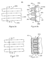
In FIGS. 9a and 9 b, a silicon body 200 is shown that is doped p-type uniformly in the direction extending along the surface of the wafer in the area of the array. A thin oxide 204 that forms the gate of the floating gate MOS memory transistor in disposed on the surface of the silicon body 200. Because oxide 204 is not exposed to high electric fields during operation, stress induced leakage current will not be generated and the gate oxide can be scaled toward the intrinsic limit of about 5 nm for retention. A layer of silicon is deposited on the oxide 204 and patterned with known means to form parallel traces 206. The silicon body 200 is implanted with an n-type dopant, preferably an n-type dopant with low rate of thermal diffusion such as Arsenic (As) or Antimony (Sb), to form doped regions 202 in the spaces between the silicon traces 206. The dopant may serve to dope the silicon traces 206, but the traces 206 serve to mask the regions under the traces 206.
In FIGS. 10A and 10B, after the implant is performed, an oxide/nitride/oxide, ONO, dielectric 208 is formed by one of several methods known in the art. It is preferred that the method employed does not expose the n-type implant 202 to high temperature treatment. A second layer of silicon 210 is deposited and doped either in situ or subsequent to deposition. A layer of silicon nitride is deposited on the second layer of silicon 210 and capped with a layer of deposited oxide to form the sandwich layer 212. The oxide layer in the sandwich layer 212 should be substantially thicker than the top layer of oxide in the ONO stack, preferably about 50 nm thick.
In FIGS. 11a through 11 d, the sandwich layer 212 and underlying silicon layer 210 are then patterned into a series of parallel traces 218 that run perpendicular to the traces 206. A thin layer of silicon oxide 216, preferably about 20 nm thick, is grown on the side walls of the second layer silicon traces 218. The ONO dielectric prevents oxidation of the first layer silicon traces 206 or the underlying silicon body 200 during this process.
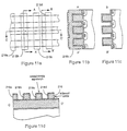
In FIGS. 12a through 12 d, after the sidewall oxide 216 is grown on the second layer silicon traces, the ONO and underlying first layer silicon traces 206 exposed between the traces 218 of the second layer of silicon are etched away in an anisotropic etch. An implant of boron is made into the exposed regions 220 to raise the thresholds of these regions to provide isolation between the remaining portions of the first layer silicon traces 206 in the direction perpendicular to the second layer silicon traces 218. These remaining portions of the first layer silicon traces 206 form the floating gates of the floating gate memory transistors.
In FIGS. 13a through 13 d, a layer of oxide 222 that forms a retention oxide is then deposited and annealed. A grid conductor 224 is deposited on oxide 222. As discussed previously, the grid conductor 224 may be any metal, alloy, or metallic compound that has the appropriate work function, conductivity, and range for “hot” carriers. The grid conductor 224 should be thin enough to allow a desired fraction of hot carriers to pass through without losing energy.
In FIGS. 14a through 14 d, the grid conductor 224 is anisotropically etched to leave it only along the sidewalls of the first and second traces of the silicon layers 206 and 218 as is seen in FIG. 14d.
In FIGS. 15a through 15 d, a tunnel layer silicon oxide 226 of about 5 nm is deposited so that it covers the grid electrode 224. Although silicon oxide is used in this embodiment, the tunnel insulating layer could be any one of or a combination of silicon nitride, silicon oxide, aluminum oxide, or other such insulator with a high dielectric strength that is compatible with integrated circuit processing technology.
In FIGS. 16a through 16 d, the injector conductor 228 is deposited by a method which will fill the space between the silicon traces and provide a reasonably smooth surface. The thickness of the injector conductor 228 should be more than 50% of the spacing between the silicon traces and preferably about 75% of this spacing. For example, if the spacing between the traces is 100 mn, the injector conductor thickness is preferably 75 nm.
In FIGS. 17a through 17 e, the material of the injector conductor 228 is then etched back to expose the tops of the traces so that the material of the injector conductor 228 lying in the channels between silicon traces is isolated from material of the injector conductor 228 lying in adjacent channels.
In FIGS. 18a through 18 e, an isolating layer 230, of preferably either silicon nitride layer or a sandwich layer of a tin layer of silicon nitride under silicon oxide is deposited and selectively removed from the surface above every other channel. The channels that remain covered implement hole emitters. After the insulator 230 is selectively removed, a conducting layer 232 is deposited that is preferably a thin layer of titanium nitride covered with aluminum. The conducting layer 232 is selectively etched into traces with the aid of a photoresist mask. While the mask is in place, exposed material of the injector conductor 228 is etched from between the traces. The traces are placed so that the islands of material of the injector conductor 228 contacting the conducting traces 232 are adjacent to floating gates. These islands are the electron injectors.
In this structure, the second layer silicon traces 218 implement word lines, the diffused regions 202 implement source and drain regions of the floating gate MOS memory transistors. The hole emitters run along the word lines so that individual word lines, blocks of word lines or an entire array can be erased simultaneously, depending on the biasing of the grid lines, the injector lines, and the word lines. The duration required to erase a row should be on the order of μsec. Further, because the traces that set the injector biases for the electron injectors run perpendicular to those that set the bias for associated grids, the electron injectors can be individually addressed to permit the programming of individual cells.
The size of each cell is the minimum pitch in each direction so that the individual cell occupies an area of 4l2, wherein l is the minimum feature size. For example, in a technology having a minimum feature size of 0.1 μm, the cell size would be on the order of 0.01 μm2 so that 108 cells could be packed into 1 mm2. Moreover, because the cells can be written with biases of about ±3.5 V, the supporting circuitry can be made compatible with scaled technology.
An additional advantage of this technology is that the carriers that are injected over the retention barrier are fairly tightly bunched in energy. As a result, if the bias across the retention insulator is attractive, carriers will be collected with high efficiency. If the floating gate is charged so that the field across the retention insulator is repulsive, very few carriers will be collected. This permits control of the charging of the potential on the floating gate in bands of a few tenths of a volt so that storing multiple bits per cell is feasible.
While embodiments and applications of this invention have been shown and described, it would be apparent to those skilled in the art that many more modifications than mentioned above are now possible without departing from the inventive concepts herein. The invention, therefore, is not to be restricted except in the spirit of the appended claims.

Claims (43)

What is claimed is:
1. A nonvolatile memory cell comprising:
a floating gate MOS transistor including:
a semiconductor body having a doping of a first type;
first and second semiconductor regions having a doping of a second type, said first and second semiconductor regions spaced apart to form a channel region in between said first and second semiconductor regions in said semiconductor body;
a floating gate disposed above said channel region in said semiconductor body;
a floating gate dielectric disposed between said floating gate and said semiconductor conductor body;
a control gate;
a control gate dielectric disposed between said control gate and said floating gate; and
a tunneling charge injector including:
a conducting injector electrode from which charge is emitted;
a grid insulator disposed adjacent to said conducting injector electrode;
a grid electrode disposed adjacent to said grid insulator; and
a retention insulator disposed adjacent to said grid electrode, wherein said floating gate is disposed adjacent to said retention insulator and said tunneling charge injector is disposed along a side of said floating gate and separated therefrom by said grid insulator, said grid electrode and said retention insulator.
2. A nonvolatile memory cell as in claim 1, wherein said floating gate comprises polysilicon.
3. A nonvolatile memory cell as in claim 1, wherein said retention insulator is formed of a layer of silicon oxide having a thickness in a range of about 8 nm to about 50 nm.
4. A nonvolatile memory cell as in claim 1, wherein said grid electrode is thin enough to minimize loss of energy of injected charge carriers and thick enough to conduct away charge carriers that lose energy and are thermalized in said grid electrode.
5. A nonvolatile memory cell as in claim 1, wherein said grid electrode has a thickness in a range of about 10 nm to about 50 nm.
6. A nonvolatile memory cell as in claim 2, wherein said grid electrode comprises a metal having a work function with a fermi level that in a flat band condition lies in approximately the middle of a band gap of said floating gate electrode.
7. A nonvolatile memory cell as in claim 1, wherein said grid electrode is formed of a metal selected from the group consisting of: Cr, Ni, Cu, and W.
8. A nonvolatile memory cell as in claim 1, wherein said grid insulator is formed of a layer of silicon oxide having a thickness in a range of about 3 nm to about 6 nm.
9. A nonvolatile memory cell as in claim 1, wherein said grid insulator has a thickness through which charge carriers will tunnel with application across the grid insulator of a bias in a range of about 2 V to about 6 V.
10. A nonvolatile memory cell as in claim 1, wherein said conducting injector electrode comprises a metal having a work function with a fermi level that in a flat band condition lies in approximately the middle of a band gap of said floating gate.
11. A nonvolatile memory cell as in claim 1, wherein said conducting injector electrode is formed of a metal selected from the group consisting of: Cr, Ni, Cu, and W.
12. A nonvolatile memory cell as in claim 1, wherein application of a negative bias from said injector electrode with respect to said grid electrode will result in electrons tunneling from said conducting injector electrode to said grid electrode.
13. A nonvolatile memory cell as in claim 1, wherein the application of a positive bias from said conducting injector electrode with respect to said grid electrode will result in holes tunneling from said injector electrode to said grid electrode.
14. A nonvolatile memory cell as in claim 1, wherein application of a negative bias from said injector electrode with respect to said grid electrode raises a fermi level of said injector electrode to cause electrons to tunnel into said grid electrode with enough energy to pass into a conduction band of said retention insulator.
15. A nonvolatile memory cell as in claim 1, wherein application of a positive bias from said conducting injector electrode with respect to said grid electrode lowers a fermi level of said injector electrode to cause holes to tunnel into said grid electrode with enough energy to pass into valence band of said retention insulator.
16. A nonvolatile memory cell comprising:
a floating gate MOS transistor including:
a semiconductor body having a doping of a first type;
first and second semiconductor regions having a doping of a second type, said first and second semiconductor regions spaced apart to form a channel region in between said first and second semiconductor regions in said semiconductor body;
a floating gate disposed above said channel region in said semiconductor body;
a floating gate dielectric disposed between said floating gate and said semiconductor body;
a control gate; and
a control gate dielectric disposed between said control gate and said floating gate;
a tunneling electron injector including:
a first conducting injector electrode from which electrons are emitted;
a first grid insulator disposed adjacent to said first conducting injector electrode;
a first grid electrode disposed adjacent to said first grid insulator; and
a first retention insulator disposed adjacent to said first grid electrode, wherein said floating gate is disposed adjacent to said first retention insulator and said tunneling electron injector is disposed along a first side of said floating gate and separated therefrom by said first grid insulator, said first grid electrode and said first retention insulator; and
a tunneling hole injector including:
a second conducting injector electrode from which holes are emitted;
a second grid insulator disposed adjacent to said second conducting injector electrode;
a second grid electrode disposed adjacent to said second grid insulator; and
a second retention insulator disposed adjacent to said second grid electrode wherein said floating gate is disposed adjacent to said second retention insulator and said tunneling hole injector is disposed along a second side of said floating gate and separated therefrom by said second grid insulator, said second grid electrode and said second retention insulator.
17. A nonvolatile memory cell as in claim 16, wherein said floating gate has a conduction band edge and a valence band edge similar to a conduction band edge and a valence band edge of said first conducting injector electrode.
18. A nonvolatile memory cell as in claim 16, wherein said floating gate comprises polysilicon.
19. A nonvolatile memory cell as in claim 16, wherein said first retention insulator is formed of a layer of silicon oxide having a thickness in a range of about 8 nm to about 50 nm.
20. A nonvolatile memory cell as in claim 16, wherein said first grid electrode is thin enough to minimize loss of energy of injected charge carriers and thick enough to conduct away charge carriers that lose energy and are thermalized in said first grid electrode.
21. A nonvolatile memory cell as in claim 16, wherein said first grid electrode has a thickness in a range of about 10 nm to 50 nm.
22. A nonvolatile memory cell as in claim 18, wherein said first grid electrode comprises a metal having a work function with a fermi level that in a flat band condition lies in approximately the middle of band gap of said floating gate.
23. A nonvolatile memory cell as in claim 16, wherein said first grid electrode is formed of a metal selected from the group consisting of Cr, Ni, Cu, and W.
24. A nonvolatile memory cell as in claim 16, wherein said first grid insulator is formed of a layer of silicon oxide having a thickness in a range of about 3 nm to about 6 nm.
25. A nonvolatile memory cell as in claim 16, wherein said first grid insulator has a thickness through which charge carriers will tunnel with application across said first grid insulator of a bias in a range of about 2 V to about 6 V.
26. A nonvolatile memory cell as in claim 16, wherein said first conducting injector electrode comprises n-type doped silicon.
27. A nonvolatile memory cell as in claim 26, wherein application of a negative bias from said first conducting injector electrode with respect to said first grid electrode will result in electrons tunneling from said first conducting injector electrode to said first grid electrode.
28. A nonvolatile memory cell as in claim 26, wherein application of a negative bias from said first conducting injector electrode with respect to said first grid electrode raises a conduction band of said first conducting injector electrode above a conduction band of said first retention insulator.
29. A nonvolatile memory cell as in claim 16, wherein said second retention insulator is formed of a layer of silicon oxide having a thickness in a range of about 8 nm to about 50 nm.
30. A nonvolatile memory cell as in claim 16, wherein said second grid electrode is thin enough to minimize loss of energy of injected charge carriers and thick enough to conduct away charge carriers that lose energy and are thermalized in said second grid electrode.
31. A nonvolatile memory cell as in claim 16, wherein said second grid electrode has a thickness in a range of about 10 nm to 50 nm.
32. A nonvolatile memory cell as in claim 16, wherein said second grid electrode comprises a metal having a work function with a fermi level that in a flat band condition lies in approximately the middle of a band gap of said floating gate.
33. A nonvolatile memory cell as in claim 16, wherein said second grid electrode is formed of a metal selected from the group consisting of: Pt, Cr, Ni, Cu, and W.
34. A nonvolatile memory cell as in claim 16, wherein said second grid insulator is formed of a layer of silicon oxide having a thickness in a range of about 3 nm to about 6 nm.
35. A nonvolatile memory cell as in claim 16, wherein said second grid insulator has a thickness through which charge carriers will tunnel with application across said second grid insulator of a bias in a range of about 2 V to about 6 V.
36. A nonvolatile memory cell as in claim 16, wherein said second conducting injector electrode comprises a metal having a work function that is greater than a work function of a metal of which said second grid electrode is comprised.
37. A nonvolatile memory cell as in claim 16, wherein application of a positive bias from said second conducting injector electrode with respect to said second grid electrode will result in holes tunneling from said second conducting injector electrode to said second grid electrode.
38. A nonvolatile memory cell as in claim 16, wherein said second conducting injector electrode comprises Pt.
39. A nonvolatile memory cell as in claim 38, wherein application of a positive bias from said second conducting injector electrode with respect to said second grid electrode lowers a fermi level of said second conducting injector electrode below a valence band of said second retention insulator.
40. A nonvolatile memory cell as in claim 16, wherein said second conducting injector electrode comprises p-type doped silicon.
41. A nonvolatile memory cell as in claim 40, wherein application of a positive bias from said second conducting injector electrode with respect to said second grid electrode lowers a valence band of said second conducting injector electrode below a valence band of said second retention insulator.
42. A nonvolatile memory device comprising:
a plurality of nonvolatile memory elements arranged in a rectangular array of rows and columns, each of said plurality of non volatile memory elements including:
a floating gate MOS transistor having a source region and a drain region formed in a semiconductor body and spaced apart by a channel region, a floating gate disposed above said channel region, and a control gate for said floating gate; and
a tunneling charge injector having a conducting injector electrode, a grid insulator disposed adjacent to said conducting injector electrode, a grid electrode disposed adjacent to said grid insulator, and a retention insulator disposed adjacent to said grid electrode, wherein said floating gate is disposed adjacent to said retention insulator and said tunneling charge injector is disposed along a side of said floating gate and separated therefrom by said grid insulator, said grid electrode and said retention insulator;
a plurality of word lines, a separate one of said plurality of word lines coupled to said control gate of each of said plurality of nonvolatile memory cells in a same row;
a plurality of bit lines, a separate one of said plurality of bit lines coupled to said drain region of each of said plurality of nonvolatile memory cells in a same column;
a plurality of source lines, at least one of said plurality of source lines coupled to said source region of each of said plurality of nonvolatile memory cells in a same row;
a plurality of injector lines, at least one of said plurality of injector lines coupled to said conducting injector electrode of each of said plurality of nonvolatile memory cells in a same row; and
a plurality of grid lines, at least one of said plurality of grid lines coupled to said grid electrode of each of said plurality of nonvolatile memory cells in a same column.
43. A nonvolatile memory device comprising:
a plurality of nonvolatile memory elements arranged in a rectangular array of rows and columns, each of said plurality of nonvolatile memory elements including:
a floating gate MOS transistor having a source region and a drain region formed in a semiconductor body and spaced apart by a channel region, a floating gate disposed above said channel region, and a control gate for said floating gate; and
a tunneling electron injector having a first conducting injector electrode, a first grid insulator disposed adjacent to said first conducting injector electrode, a first grid electrode disposed adjacent to said first grid insulator, and a first retention insulator disposed adjacent to said first grid electrode, wherein said floating gate is disposed adjacent to said first retention insulator and said tunneling electron injector is disposed along a first side of said floating gate and separated therefrom by said first grid insulator, said first grid electrode and said first retention insulator;
a tunneling hole injector having a second conducting injector electrode, a second grid insulator disposed adjacent to said second conducting injector electrode, a second grid electrode disposed adjacent to said second grid insulator, and a second retention insulator disposed adjacent to said second grid electrode, wherein said floating gate is disposed adjacent to said second retention insulator and said tunneling hole injector is disposed along a second side of said floating gate and separated therefrom by said second grid insulator, said second grid electrode and said second retention insulator;
a plurality of word lines, a separate one of said plurality of word lines coupled to said control gate of each of said plurality of nonvolatile memory cells in a same row;
a plurality of bit lines, a separate one of said plurality of bit lines coupled to said drain region of each of said plurality of nonvolatile memory cells in a same column;
a plurality of source lines, at least one of said plurality of source lines coupled to said source region of each of said plurality of nonvolatile memory cells in a same row;
a first plurality of injector lines, at least one of said first plurality of injector lines coupled to said first conducting injector electrode of each of said plurality of nonvolatile memory cells in a same row;
a first plurality of grid lines, at least one of said first plurality of grid lines coupled to said first grid electrode of each of said plurality of nonvolatile memory cells in a same column;
a second plurality of injector lines, at least one of said second plurality of injector lines coupled to said second conducting injector electrode of each of said plurality of nonvolatile memory cells in a same row; and
a second plurality of grid lines, at least one of said second plurality of grid lines coupled to said second grid electrode of each of said plurality of nonvolatile memory cells in a same column.
US09/731,942 1999-03-24 2000-12-06 Method and apparatus for injecting charge onto the floating gate of a nonvolatile memory cell Expired - Lifetime US6479863B2 (en)

Priority Applications (2)

Application Number Priority Date Filing Date Title
US09/731,942 US6479863B2 (en) 1999-03-24 2000-12-06 Method and apparatus for injecting charge onto the floating gate of a nonvolatile memory cell
US09/942,338 US20040021170A1 (en) 1999-03-24 2001-08-28 Method and apparatus for injecting charge onto the floating gate of a nonvolatile memory cell

Applications Claiming Priority (3)

Application Number Priority Date Filing Date Title
US27516899A 1999-03-24 1999-03-24
US09/522,252 US6384451B1 (en) 1999-03-24 2000-03-09 Method and apparatus for injecting charge onto the floating gate of a nonvolatile memory cell
US09/731,942 US6479863B2 (en) 1999-03-24 2000-12-06 Method and apparatus for injecting charge onto the floating gate of a nonvolatile memory cell

Related Parent Applications (1)

Application Number Title Priority Date Filing Date
US09/522,252 Continuation US6384451B1 (en) 1999-03-24 2000-03-09 Method and apparatus for injecting charge onto the floating gate of a nonvolatile memory cell

Related Child Applications (1)

Application Number Title Priority Date Filing Date
US09/552,252 Continuation US7102056B1 (en) 1997-04-29 2000-04-18 Compositions and methods for plant transformation and regeneration

Publications (2)

Publication Number Publication Date
US20010019151A1 US20010019151A1 (en) 2001-09-06
US6479863B2 true US6479863B2 (en) 2002-11-12

Family

ID=23051158

Family Applications (2)

Application Number Title Priority Date Filing Date
US09/522,252 Expired - Lifetime US6384451B1 (en) 1999-03-24 2000-03-09 Method and apparatus for injecting charge onto the floating gate of a nonvolatile memory cell
US09/731,942 Expired - Lifetime US6479863B2 (en) 1999-03-24 2000-12-06 Method and apparatus for injecting charge onto the floating gate of a nonvolatile memory cell

Family Applications Before (1)

Application Number Title Priority Date Filing Date
US09/522,252 Expired - Lifetime US6384451B1 (en) 1999-03-24 2000-03-09 Method and apparatus for injecting charge onto the floating gate of a nonvolatile memory cell

Country Status (1)

Country Link
US (2) US6384451B1 (en)

Cited By (25)

* Cited by examiner, † Cited by third party
Publication number Priority date Publication date Assignee Title
US20030206437A1 (en) * 1995-03-07 2003-11-06 California Institute Of Technology, A California Non-Profit Corporation Floating-gate semiconductor structures
US20040004863A1 (en) * 2002-07-05 2004-01-08 Chih-Hsin Wang Nonvolatile electrically alterable memory device and array made thereby
US20040021170A1 (en) * 1999-03-24 2004-02-05 Caywood John M. Method and apparatus for injecting charge onto the floating gate of a nonvolatile memory cell
US20040021166A1 (en) * 2002-05-09 2004-02-05 Impinj, Inc., A Delaware Corporation Pseudo-nonvolatile direct-tunneling floating-gate device
US20040037127A1 (en) * 2002-07-05 2004-02-26 Impinj, Inc., A Delaware Corporation Differential floating gate nonvolatile memories
US20040173842A1 (en) * 1999-04-26 2004-09-09 Akira Goda Nonvolatile semiconductor memory device and method for manufacturing the same
US20040248371A1 (en) * 2003-06-06 2004-12-09 Chih-Hsin Wang Floating-gate memory cell having trench structure with ballastic-charge injector and array of memory cells
US20050063235A1 (en) * 2002-07-05 2005-03-24 Impinj, Inc., A Delaware Corporation PFET nonvolatile memory
US20050201150A1 (en) * 2003-06-06 2005-09-15 Chih-Hsin Wang Method and apparatus for semiconductor device and semiconductor memory device
US20060262600A1 (en) * 2002-05-10 2006-11-23 Riichiro Shirota Non-Volatile semiconductor memory device
US20060289924A1 (en) * 2005-06-28 2006-12-28 Chih-Hsin Wang Low power electrically alterable nonvolatile memory cells and arrays
US20070263456A1 (en) * 2005-03-17 2007-11-15 Impinj, Inc. Inverter non-volatile memory cell and array system
US20070281425A1 (en) * 2003-06-06 2007-12-06 Chih-Hsin Wang Method and apparatus transporting charges in semiconductor device and semiconductor memory device
US7613041B2 (en) 2003-06-06 2009-11-03 Chih-Hsin Wang Methods for operating semiconductor device and semiconductor memory device
US7679957B2 (en) 2005-03-31 2010-03-16 Virage Logic Corporation Redundant non-volatile memory cell
US7759719B2 (en) 2004-07-01 2010-07-20 Chih-Hsin Wang Electrically alterable memory cell
US7796450B1 (en) 2007-04-24 2010-09-14 Virage Logic Corporation Radio frequency (RFID) tag including configurable single bit/dual bits memory
US20100259985A1 (en) * 2006-11-01 2010-10-14 Gumbo Logic, Inc. Trap-charge non-volatile switch connector for programmable logic
US8072023B1 (en) 2007-11-12 2011-12-06 Marvell International Ltd. Isolation for non-volatile memory cell array
US8077511B2 (en) 2004-04-21 2011-12-13 Synopsys, Inc. Hybrid non-volatile memory
US8102007B1 (en) 2001-08-13 2012-01-24 Synopsys, Inc. Apparatus for trimming high-resolution digital-to-analog converter
US8111558B2 (en) 2004-05-05 2012-02-07 Synopsys, Inc. pFET nonvolatile memory
US8120088B1 (en) 2007-12-07 2012-02-21 Marvell International Ltd. Non-volatile memory cell and array
US8122307B1 (en) 2006-08-15 2012-02-21 Synopsys, Inc. One time programmable memory test structures and methods
US8139411B1 (en) 2008-05-22 2012-03-20 Synopsys, Inc. pFET nonvolatile memory

Families Citing this family (13)

* Cited by examiner, † Cited by third party
Publication number Priority date Publication date Assignee Title
US6242306B1 (en) * 2000-07-28 2001-06-05 Advanced Micro Devices Dual bit isolation scheme for flash memory devices having polysilicon floating gates
US6462372B1 (en) * 2001-10-09 2002-10-08 Silicon-Based Technology Corp. Scaled stack-gate flash memory device
US6580642B1 (en) 2002-04-29 2003-06-17 Silicon Storage Technology, Inc. Method of erasing nonvolatile tunneling injector memory cell
DE10229065A1 (en) * 2002-06-28 2004-01-29 Infineon Technologies Ag Method for producing an NROM memory cell array
US6660588B1 (en) 2002-09-16 2003-12-09 Advanced Micro Devices, Inc. High density floating gate flash memory and fabrication processes therefor
US7115942B2 (en) * 2004-07-01 2006-10-03 Chih-Hsin Wang Method and apparatus for nonvolatile memory
US7145370B2 (en) * 2003-09-05 2006-12-05 Impinj, Inc. High-voltage switches in single-well CMOS processes
US7242614B2 (en) * 2004-03-30 2007-07-10 Impinj, Inc. Rewriteable electronic fuses
US7388420B2 (en) * 2004-03-30 2008-06-17 Impinj, Inc. Rewriteable electronic fuses
US7177182B2 (en) * 2004-03-30 2007-02-13 Impinj, Inc. Rewriteable electronic fuses
US20080203464A1 (en) * 2004-07-01 2008-08-28 Chih-Hsin Wang Electrically alterable non-volatile memory and array
CN100373625C (en) * 2004-12-03 2008-03-05 马维尔世界贸易股份有限公司 Erasable and programmable read-only memory element and producing and operating method
US20060197144A1 (en) * 2005-03-01 2006-09-07 Mammen Thomas Nitride storage cells with and without select gate

Citations (28)

* Cited by examiner, † Cited by third party
Publication number Priority date Publication date Assignee Title
US3778645A (en) 1972-01-31 1973-12-11 Univ Virginia Solid-state switching capacitor
US4035820A (en) 1975-12-29 1977-07-12 Texas Instruments Incorporated Adjustment of avalanche voltage in DIFMOS memory devices by control of impurity doping
US4037242A (en) 1975-12-29 1977-07-19 Texas Instruments Incorporated Dual injector, floating gate MOS electrically alterable, non-volatile semiconductor memory device
US4513397A (en) 1982-12-10 1985-04-23 Rca Corporation Electrically alterable, nonvolatile floating gate memory device
US4626887A (en) 1983-08-19 1986-12-02 Siemens Aktiengesellschaft Static storage cell
US4630081A (en) 1984-12-19 1986-12-16 Eaton Corporation MOMOM tunnel emission transistor
US4686558A (en) 1982-09-15 1987-08-11 Itt Industries, Inc. CMOS memory cell having an electrically floating storage gate
US4752912A (en) 1985-05-14 1988-06-21 Xicor, Inc. Nonvolatile electrically alterable memory and method
JPS6476766A (en) * 1987-09-17 1989-03-22 Nec Corp Superconducting field-effect transistor
US4907198A (en) 1987-12-02 1990-03-06 Mitsubishi Denki Kabushiki Kaisha Semiconductor memory device
US4907197A (en) 1987-07-13 1990-03-06 Oki Electric Industry Co., Ltd. Non-volatile semiconductor memory device
US4910565A (en) 1980-11-20 1990-03-20 Tokyo Shibaura Denki Kabushiki Kaisha Electrically erasable and electrically programmable read-only memory
US4924437A (en) 1987-12-09 1990-05-08 Texas Instruments Incorporated Erasable programmable memory including buried diffusion source/drain lines and erase lines
US4967393A (en) 1987-02-20 1990-10-30 Kabushiki Kaisha Toshiba Flash erasable and programmable nonvolatile semiconductor memory
US5101249A (en) 1979-08-31 1992-03-31 Fujitsu Limited Nonvolatile semiconductor memory device
US5111430A (en) 1989-06-22 1992-05-05 Nippon Telegraph And Telephone Corporation Non-volatile memory with hot carriers transmitted to floating gate through control gate
US5235544A (en) 1990-11-09 1993-08-10 John Caywood Flash EPROM cell and method for operating same
US5338952A (en) 1991-06-07 1994-08-16 Sharp Kabushiki Kaisha Non-volatile memory
US5347143A (en) * 1991-05-17 1994-09-13 Dornier Luftfahrt Gmbh Tunnelling barrier between two non-tunnelling superconductor-insulator-controlling superconductor-insulator-superconductor structures
US5359571A (en) 1993-01-27 1994-10-25 Yu Shih Chiang Memory array having a plurality of address partitions
US5517044A (en) * 1992-02-07 1996-05-14 Nec Corporation Non-volatile semiconductor memory device having thin film transistors equipped with floating gates
US5679970A (en) * 1992-07-03 1997-10-21 Commissariat A L'energie Atomique Triple gate flash-type EEPROM memory and its production process
US5838039A (en) 1995-07-14 1998-11-17 Matsushita Electronics Corporation Semiconductor memory having a tunneling region
US5841161A (en) 1996-04-12 1998-11-24 Lg Semicon Co., Ltd. Flash memory and method for fabricating the same
US5946240A (en) 1996-12-25 1999-08-31 Nec Corporation Nonvolatile semiconductor memory device and method of manufacturing the same
JP2964412B2 (en) 1989-06-22 1999-10-18 日本電信電話株式会社 Non-volatile memory
US5977586A (en) 1992-09-30 1999-11-02 Stmicroelectronics S.R.L. Non-volatile integrated low-doped drain device with partially overlapping gate regions
US6002152A (en) 1992-01-14 1999-12-14 Sandisk Corporation EEPROM with split gate source side injection with sidewall spacers

Patent Citations (28)

* Cited by examiner, † Cited by third party
Publication number Priority date Publication date Assignee Title
US3778645A (en) 1972-01-31 1973-12-11 Univ Virginia Solid-state switching capacitor
US4035820A (en) 1975-12-29 1977-07-12 Texas Instruments Incorporated Adjustment of avalanche voltage in DIFMOS memory devices by control of impurity doping
US4037242A (en) 1975-12-29 1977-07-19 Texas Instruments Incorporated Dual injector, floating gate MOS electrically alterable, non-volatile semiconductor memory device
US5101249A (en) 1979-08-31 1992-03-31 Fujitsu Limited Nonvolatile semiconductor memory device
US4910565A (en) 1980-11-20 1990-03-20 Tokyo Shibaura Denki Kabushiki Kaisha Electrically erasable and electrically programmable read-only memory
US4686558A (en) 1982-09-15 1987-08-11 Itt Industries, Inc. CMOS memory cell having an electrically floating storage gate
US4513397A (en) 1982-12-10 1985-04-23 Rca Corporation Electrically alterable, nonvolatile floating gate memory device
US4626887A (en) 1983-08-19 1986-12-02 Siemens Aktiengesellschaft Static storage cell
US4630081A (en) 1984-12-19 1986-12-16 Eaton Corporation MOMOM tunnel emission transistor
US4752912A (en) 1985-05-14 1988-06-21 Xicor, Inc. Nonvolatile electrically alterable memory and method
US4967393A (en) 1987-02-20 1990-10-30 Kabushiki Kaisha Toshiba Flash erasable and programmable nonvolatile semiconductor memory
US4907197A (en) 1987-07-13 1990-03-06 Oki Electric Industry Co., Ltd. Non-volatile semiconductor memory device
JPS6476766A (en) * 1987-09-17 1989-03-22 Nec Corp Superconducting field-effect transistor
US4907198A (en) 1987-12-02 1990-03-06 Mitsubishi Denki Kabushiki Kaisha Semiconductor memory device
US4924437A (en) 1987-12-09 1990-05-08 Texas Instruments Incorporated Erasable programmable memory including buried diffusion source/drain lines and erase lines
US5111430A (en) 1989-06-22 1992-05-05 Nippon Telegraph And Telephone Corporation Non-volatile memory with hot carriers transmitted to floating gate through control gate
JP2964412B2 (en) 1989-06-22 1999-10-18 日本電信電話株式会社 Non-volatile memory
US5235544A (en) 1990-11-09 1993-08-10 John Caywood Flash EPROM cell and method for operating same
US5347143A (en) * 1991-05-17 1994-09-13 Dornier Luftfahrt Gmbh Tunnelling barrier between two non-tunnelling superconductor-insulator-controlling superconductor-insulator-superconductor structures
US5338952A (en) 1991-06-07 1994-08-16 Sharp Kabushiki Kaisha Non-volatile memory
US6002152A (en) 1992-01-14 1999-12-14 Sandisk Corporation EEPROM with split gate source side injection with sidewall spacers
US5517044A (en) * 1992-02-07 1996-05-14 Nec Corporation Non-volatile semiconductor memory device having thin film transistors equipped with floating gates
US5679970A (en) * 1992-07-03 1997-10-21 Commissariat A L'energie Atomique Triple gate flash-type EEPROM memory and its production process
US5977586A (en) 1992-09-30 1999-11-02 Stmicroelectronics S.R.L. Non-volatile integrated low-doped drain device with partially overlapping gate regions
US5359571A (en) 1993-01-27 1994-10-25 Yu Shih Chiang Memory array having a plurality of address partitions
US5838039A (en) 1995-07-14 1998-11-17 Matsushita Electronics Corporation Semiconductor memory having a tunneling region
US5841161A (en) 1996-04-12 1998-11-24 Lg Semicon Co., Ltd. Flash memory and method for fabricating the same
US5946240A (en) 1996-12-25 1999-08-31 Nec Corporation Nonvolatile semiconductor memory device and method of manufacturing the same

Non-Patent Citations (7)

* Cited by examiner, † Cited by third party
Title
Dons, et al., "Direct Tunneling Diode Structure with a Multi-Layer Charge Injection Barrier", 29th IEEE Semiconductor Interface Specialists Conference (1998).
Guo, Xin, "Tunneling Leakage Current in Oxynitride: Dependence on Oxygen/Nitrogen Content", IEEE, Electron Device Letters, vol. 19, No. 6, pp. 207-209 (1998).
Huber et al, "Hot-Electron Transport in Al-Al2O3 Triodes Produced by Plasma Oxidation", Journal of Applied Physics, vol. 39, No. 11, pp. 5104-5116 (1968).
Krolikowski, "Photoemission Studies of the Noble Metals II. Gold", Physical Review B, vol. 1, No. 2, pp. 478-487 (1970).
Krolikowski, "Photoemission Studies of the Noble Metals. I. Copper", Physical Review, vol. 185, No. 3, pp. 882-900 (1969).
Mead, "Operation of Tunnel-Emission Devices", J. Appl. Phys., vol. 32, No. 4 (1961).
Mead, "The Tunnel-Emission Amplifier", Proceedings of IRE, pp. 359-361 (1960).

Cited By (54)

* Cited by examiner, † Cited by third party
Publication number Priority date Publication date Assignee Title
US7548460B2 (en) 1995-03-07 2009-06-16 California Institute Of Technology Floating-gate semiconductor structures
US6965142B2 (en) 1995-03-07 2005-11-15 Impinj, Inc. Floating-gate semiconductor structures
US7098498B2 (en) 1995-03-07 2006-08-29 California Institute Of Technology Floating-gate semiconductor structures
US20030206437A1 (en) * 1995-03-07 2003-11-06 California Institute Of Technology, A California Non-Profit Corporation Floating-gate semiconductor structures
US20050104119A1 (en) * 1995-03-07 2005-05-19 California Institute Of Technology, A California Non-Profit Corporation Floating-gate semiconductor structures
US20050099859A1 (en) * 1995-03-07 2005-05-12 California Institute Of Technology, A California Non-Profit Corporation Floating-gate semiconductor structures
US20040021170A1 (en) * 1999-03-24 2004-02-05 Caywood John M. Method and apparatus for injecting charge onto the floating gate of a nonvolatile memory cell
US20060157801A1 (en) * 1999-04-26 2006-07-20 Akira Goda Nonvolatile semiconductor memory device and method for manufacturing the same
US20040173842A1 (en) * 1999-04-26 2004-09-09 Akira Goda Nonvolatile semiconductor memory device and method for manufacturing the same
US7095085B2 (en) * 1999-04-26 2006-08-22 Kabushiki Kaisha Toshiba Nonvolatile semiconductor memory device and method for manufacturing the same
US7364951B2 (en) * 1999-04-26 2008-04-29 Kabushiki Kaisha Toshiba Nonvolatile semiconductor memory device and method for manufacturing the same
US8102007B1 (en) 2001-08-13 2012-01-24 Synopsys, Inc. Apparatus for trimming high-resolution digital-to-analog converter
US20040021166A1 (en) * 2002-05-09 2004-02-05 Impinj, Inc., A Delaware Corporation Pseudo-nonvolatile direct-tunneling floating-gate device
US20060262600A1 (en) * 2002-05-10 2006-11-23 Riichiro Shirota Non-Volatile semiconductor memory device
US20040037127A1 (en) * 2002-07-05 2004-02-26 Impinj, Inc., A Delaware Corporation Differential floating gate nonvolatile memories
US7221596B2 (en) 2002-07-05 2007-05-22 Impinj, Inc. pFET nonvolatile memory
US6950342B2 (en) 2002-07-05 2005-09-27 Impinj, Inc. Differential floating gate nonvolatile memories
US20040004863A1 (en) * 2002-07-05 2004-01-08 Chih-Hsin Wang Nonvolatile electrically alterable memory device and array made thereby
US20050063235A1 (en) * 2002-07-05 2005-03-24 Impinj, Inc., A Delaware Corporation PFET nonvolatile memory
US7550800B2 (en) 2003-06-06 2009-06-23 Chih-Hsin Wang Method and apparatus transporting charges in semiconductor device and semiconductor memory device
US7741177B2 (en) 2003-06-06 2010-06-22 Chih-Hsin Wang Method and apparatus transporting charges in semiconductor device and semiconductor memory device
US7824981B2 (en) 2003-06-06 2010-11-02 Chih-Hsin Wang Method and apparatus for semiconductor device and semiconductor memory device
US20070281425A1 (en) * 2003-06-06 2007-12-06 Chih-Hsin Wang Method and apparatus transporting charges in semiconductor device and semiconductor memory device
US20080070390A1 (en) * 2003-06-06 2008-03-20 Chih-Hsin Wang Method and apparatus for semiconductor device and semiconductor memory device
US7745286B2 (en) 2003-06-06 2010-06-29 Chih-Hsin Wang Methods of forming semiconductor devices
US6958513B2 (en) 2003-06-06 2005-10-25 Chih-Hsin Wang Floating-gate memory cell having trench structure with ballistic-charge injector, and the array of memory cells
US20050201150A1 (en) * 2003-06-06 2005-09-15 Chih-Hsin Wang Method and apparatus for semiconductor device and semiconductor memory device
US7297634B2 (en) * 2003-06-06 2007-11-20 Marvell World Trade Ltd. Method and apparatus for semiconductor device and semiconductor memory device
US20040248371A1 (en) * 2003-06-06 2004-12-09 Chih-Hsin Wang Floating-gate memory cell having trench structure with ballastic-charge injector and array of memory cells
US7613041B2 (en) 2003-06-06 2009-11-03 Chih-Hsin Wang Methods for operating semiconductor device and semiconductor memory device
US8077511B2 (en) 2004-04-21 2011-12-13 Synopsys, Inc. Hybrid non-volatile memory
US8111558B2 (en) 2004-05-05 2012-02-07 Synopsys, Inc. pFET nonvolatile memory
US7759719B2 (en) 2004-07-01 2010-07-20 Chih-Hsin Wang Electrically alterable memory cell
US7791950B2 (en) 2005-03-17 2010-09-07 Virage Logic Corporation Inverter non-volatile memory cell and array system
US20070263456A1 (en) * 2005-03-17 2007-11-15 Impinj, Inc. Inverter non-volatile memory cell and array system
US7679957B2 (en) 2005-03-31 2010-03-16 Virage Logic Corporation Redundant non-volatile memory cell
US7808823B2 (en) 2005-03-31 2010-10-05 Virage Logic Corporation RFID tag with redundant non-volatile memory cell
US7411244B2 (en) 2005-06-28 2008-08-12 Chih-Hsin Wang Low power electrically alterable nonvolatile memory cells and arrays
US7719050B1 (en) 2005-06-28 2010-05-18 Chih-Hsin Wang Low power electrically alterable nonvolatile memory cells and arrays
US7547601B2 (en) 2005-06-28 2009-06-16 Marvell World Trade Ltd. Low power electrically alterable nonvolatile memory cells and arrays
US20060289924A1 (en) * 2005-06-28 2006-12-28 Chih-Hsin Wang Low power electrically alterable nonvolatile memory cells and arrays
US8122307B1 (en) 2006-08-15 2012-02-21 Synopsys, Inc. One time programmable memory test structures and methods
US20100259986A1 (en) * 2006-11-01 2010-10-14 Gumbo Logic, Inc. Trap-charge non-volatile switch connector for programmable logic
US20100259981A1 (en) * 2006-11-01 2010-10-14 Gumbo Logic, Inc. Trap-charge non-volatile switch connector for programmable logic
US20100261324A1 (en) * 2006-11-01 2010-10-14 Gumbo Logic, Inc. Trap-charge non-volatile switch connector for programmable logic
US20100259985A1 (en) * 2006-11-01 2010-10-14 Gumbo Logic, Inc. Trap-charge non-volatile switch connector for programmable logic
US8023326B2 (en) 2006-11-01 2011-09-20 Halo Lsi, Inc. Trap-charge non-volatile switch connector for programmable logic
US8027198B2 (en) 2006-11-01 2011-09-27 Halo Lsi, Inc. Trap-charge non-volatile switch connector for programmable logic
US8139410B2 (en) 2006-11-01 2012-03-20 Halo Lsi, Inc. Trap-charge non-volatile switch connector for programmable logic
US8089809B2 (en) 2006-11-01 2012-01-03 Halo Lsi, Inc. Trap-charge non-volatile switch connector for programmable logic
US7796450B1 (en) 2007-04-24 2010-09-14 Virage Logic Corporation Radio frequency (RFID) tag including configurable single bit/dual bits memory
US8072023B1 (en) 2007-11-12 2011-12-06 Marvell International Ltd. Isolation for non-volatile memory cell array
US8120088B1 (en) 2007-12-07 2012-02-21 Marvell International Ltd. Non-volatile memory cell and array
US8139411B1 (en) 2008-05-22 2012-03-20 Synopsys, Inc. pFET nonvolatile memory

Also Published As

Publication number Publication date
US6384451B1 (en) 2002-05-07
US20010019151A1 (en) 2001-09-06

Similar Documents

Publication Publication Date Title
US6479863B2 (en) Method and apparatus for injecting charge onto the floating gate of a nonvolatile memory cell
US6534816B1 (en) Method and apparatus for injecting charge onto the floating gate of a nonvolatile memory cell
US5646060A (en) Method for making an EEPROM cell with isolation transistor
US7057931B2 (en) Flash memory programming using gate induced junction leakage current
EP0530644B1 (en) Non-Volatile memory cell and fabrication method
US5969383A (en) Split-gate memory device and method for accessing the same
US6277689B1 (en) Nonvolatile memory
US6995423B2 (en) Memory device having a P+ gate and thin bottom oxide and method of erasing same
US20040021170A1 (en) Method and apparatus for injecting charge onto the floating gate of a nonvolatile memory cell
US6232634B1 (en) Non-volatile memory cell and method for manufacturing same
US7045854B2 (en) Non-volatile semiconductor memory
EP1178540B1 (en) Nonvolatile memory cell with high programming efficiency
US6482708B2 (en) Nonvolatile memory device and method for manufacturing the same
JPH07161853A (en) Nonvolatile semiconductor memory, its erasing method and manufacturing method
JPH09191057A (en) Non-volatile memory cell having pn junction formed at polysilicon floating gate and formation of memory cell
US6744105B1 (en) Memory array having shallow bit line with silicide contact portion and method of formation
US6617632B2 (en) Semiconductor device and a method of manufacturing the same
US6906959B2 (en) Method and system for erasing a nitride memory device
US7911852B2 (en) Nonvolatile semiconductor memory device and operation method thereof
US6303454B1 (en) Process for a snap-back flash EEPROM cell
US6724032B2 (en) Multi-bit non-volatile memory cell and method therefor
US7008846B2 (en) Non-volatile floating gate memory cell with floating gates formed as spacers, and an array thereof, and a method of manufacturing
US20060226467A1 (en) P-channel charge trapping memory device with sub-gate
KR19990002554A (en) Manufacturing Method of Flash Memory Array Device
KR100200074B1 (en) Fabrication method of non-volatile semiconductor memory device

Legal Events

Date Code Title Description
AS Assignment

Owner name: JOHN MILLARD AND PAMELA ANN CAYWOOD 1989 REVOCABLE

Free format text: ASSIGNMENT OF ASSIGNORS INTEREST;ASSIGNOR:CAYWOOD, JOHN MILLARD;REEL/FRAME:012645/0662

Effective date: 20020128

STCF Information on status: patent grant

Free format text: PATENTED CASE

FPAY Fee payment

Year of fee payment: 4

FPAY Fee payment

Year of fee payment: 8

FEPP Fee payment procedure

Free format text: PAYER NUMBER DE-ASSIGNED (ORIGINAL EVENT CODE: RMPN); ENTITY STATUS OF PATENT OWNER: SMALL ENTITY

FEPP Fee payment procedure

Free format text: PAYOR NUMBER ASSIGNED (ORIGINAL EVENT CODE: ASPN); ENTITY STATUS OF PATENT OWNER: SMALL ENTITY

FPAY Fee payment

Year of fee payment: 12