US6489683B1 - Variable grain size in conductors for semiconductor vias and trenches - Google Patents

Variable grain size in conductors for semiconductor vias and trenches Download PDF

Info

Publication number
US6489683B1
US6489683B1 US09/975,032 US97503201A US6489683B1 US 6489683 B1 US6489683 B1 US 6489683B1 US 97503201 A US97503201 A US 97503201A US 6489683 B1 US6489683 B1 US 6489683B1
Authority
US
United States
Prior art keywords
conductive material
channel
layer
seed layer
vias
Prior art date
Legal status (The legal status is an assumption and is not a legal conclusion. Google has not performed a legal analysis and makes no representation as to the accuracy of the status listed.)
Expired - Fee Related
Application number
US09/975,032
Inventor
Sergey D. Lopatin
John A. Iacoponi
Current Assignee (The listed assignees may be inaccurate. Google has not performed a legal analysis and makes no representation or warranty as to the accuracy of the list.)
GlobalFoundries Inc
Original Assignee
Advanced Micro Devices Inc
Priority date (The priority date is an assumption and is not a legal conclusion. Google has not performed a legal analysis and makes no representation as to the accuracy of the date listed.)
Filing date
Publication date
Application filed by Advanced Micro Devices Inc filed Critical Advanced Micro Devices Inc
Priority to US09/975,032 priority Critical patent/US6489683B1/en
Application granted granted Critical
Publication of US6489683B1 publication Critical patent/US6489683B1/en
Assigned to GLOBALFOUNDRIES INC. reassignment GLOBALFOUNDRIES INC. AFFIRMATION OF PATENT ASSIGNMENT Assignors: ADVANCED MICRO DEVICES, INC.
Anticipated expiration legal-status Critical
Assigned to GLOBALFOUNDRIES U.S. INC. reassignment GLOBALFOUNDRIES U.S. INC. RELEASE BY SECURED PARTY (SEE DOCUMENT FOR DETAILS). Assignors: WILMINGTON TRUST, NATIONAL ASSOCIATION
Expired - Fee Related legal-status Critical Current

Links

Images

Classifications

    • HELECTRICITY
    • H01ELECTRIC ELEMENTS
    • H01LSEMICONDUCTOR DEVICES NOT COVERED BY CLASS H10
    • H01L21/00Processes or apparatus adapted for the manufacture or treatment of semiconductor or solid state devices or of parts thereof
    • H01L21/70Manufacture or treatment of devices consisting of a plurality of solid state components formed in or on a common substrate or of parts thereof; Manufacture of integrated circuit devices or of parts thereof
    • H01L21/71Manufacture of specific parts of devices defined in group H01L21/70
    • H01L21/768Applying interconnections to be used for carrying current between separate components within a device comprising conductors and dielectrics
    • H01L21/76838Applying interconnections to be used for carrying current between separate components within a device comprising conductors and dielectrics characterised by the formation and the after-treatment of the conductors
    • H01L21/76877Filling of holes, grooves or trenches, e.g. vias, with conductive material
    • HELECTRICITY
    • H01ELECTRIC ELEMENTS
    • H01LSEMICONDUCTOR DEVICES NOT COVERED BY CLASS H10
    • H01L21/00Processes or apparatus adapted for the manufacture or treatment of semiconductor or solid state devices or of parts thereof
    • H01L21/02Manufacture or treatment of semiconductor devices or of parts thereof
    • H01L21/04Manufacture or treatment of semiconductor devices or of parts thereof the devices having at least one potential-jump barrier or surface barrier, e.g. PN junction, depletion layer or carrier concentration layer
    • H01L21/18Manufacture or treatment of semiconductor devices or of parts thereof the devices having at least one potential-jump barrier or surface barrier, e.g. PN junction, depletion layer or carrier concentration layer the devices having semiconductor bodies comprising elements of Group IV of the Periodic System or AIIIBV compounds with or without impurities, e.g. doping materials
    • H01L21/28Manufacture of electrodes on semiconductor bodies using processes or apparatus not provided for in groups H01L21/20 - H01L21/268
    • H01L21/283Deposition of conductive or insulating materials for electrodes conducting electric current
    • H01L21/288Deposition of conductive or insulating materials for electrodes conducting electric current from a liquid, e.g. electrolytic deposition
    • H01L21/2885Deposition of conductive or insulating materials for electrodes conducting electric current from a liquid, e.g. electrolytic deposition using an external electrical current, i.e. electro-deposition
    • HELECTRICITY
    • H01ELECTRIC ELEMENTS
    • H01LSEMICONDUCTOR DEVICES NOT COVERED BY CLASS H10
    • H01L23/00Details of semiconductor or other solid state devices
    • H01L23/52Arrangements for conducting electric current within the device in operation from one component to another, i.e. interconnections, e.g. wires, lead frames
    • H01L23/522Arrangements for conducting electric current within the device in operation from one component to another, i.e. interconnections, e.g. wires, lead frames including external interconnections consisting of a multilayer structure of conductive and insulating layers inseparably formed on the semiconductor body
    • H01L23/532Arrangements for conducting electric current within the device in operation from one component to another, i.e. interconnections, e.g. wires, lead frames including external interconnections consisting of a multilayer structure of conductive and insulating layers inseparably formed on the semiconductor body characterised by the materials
    • H01L23/53204Conductive materials
    • H01L23/53209Conductive materials based on metals, e.g. alloys, metal silicides
    • H01L23/53214Conductive materials based on metals, e.g. alloys, metal silicides the principal metal being aluminium
    • H01L23/53223Additional layers associated with aluminium layers, e.g. adhesion, barrier, cladding layers
    • HELECTRICITY
    • H01ELECTRIC ELEMENTS
    • H01LSEMICONDUCTOR DEVICES NOT COVERED BY CLASS H10
    • H01L23/00Details of semiconductor or other solid state devices
    • H01L23/52Arrangements for conducting electric current within the device in operation from one component to another, i.e. interconnections, e.g. wires, lead frames
    • H01L23/522Arrangements for conducting electric current within the device in operation from one component to another, i.e. interconnections, e.g. wires, lead frames including external interconnections consisting of a multilayer structure of conductive and insulating layers inseparably formed on the semiconductor body
    • H01L23/532Arrangements for conducting electric current within the device in operation from one component to another, i.e. interconnections, e.g. wires, lead frames including external interconnections consisting of a multilayer structure of conductive and insulating layers inseparably formed on the semiconductor body characterised by the materials
    • H01L23/53204Conductive materials
    • H01L23/53209Conductive materials based on metals, e.g. alloys, metal silicides
    • H01L23/53228Conductive materials based on metals, e.g. alloys, metal silicides the principal metal being copper
    • H01L23/53238Additional layers associated with copper layers, e.g. adhesion, barrier, cladding layers
    • HELECTRICITY
    • H01ELECTRIC ELEMENTS
    • H01LSEMICONDUCTOR DEVICES NOT COVERED BY CLASS H10
    • H01L23/00Details of semiconductor or other solid state devices
    • H01L23/52Arrangements for conducting electric current within the device in operation from one component to another, i.e. interconnections, e.g. wires, lead frames
    • H01L23/522Arrangements for conducting electric current within the device in operation from one component to another, i.e. interconnections, e.g. wires, lead frames including external interconnections consisting of a multilayer structure of conductive and insulating layers inseparably formed on the semiconductor body
    • H01L23/532Arrangements for conducting electric current within the device in operation from one component to another, i.e. interconnections, e.g. wires, lead frames including external interconnections consisting of a multilayer structure of conductive and insulating layers inseparably formed on the semiconductor body characterised by the materials
    • H01L23/53204Conductive materials
    • H01L23/53209Conductive materials based on metals, e.g. alloys, metal silicides
    • H01L23/53242Conductive materials based on metals, e.g. alloys, metal silicides the principal metal being a noble metal, e.g. gold
    • H01L23/53252Additional layers associated with noble-metal layers, e.g. adhesion, barrier, cladding layers
    • HELECTRICITY
    • H01ELECTRIC ELEMENTS
    • H01LSEMICONDUCTOR DEVICES NOT COVERED BY CLASS H10
    • H01L2924/00Indexing scheme for arrangements or methods for connecting or disconnecting semiconductor or solid-state bodies as covered by H01L24/00
    • H01L2924/0001Technical content checked by a classifier
    • H01L2924/0002Not covered by any one of groups H01L24/00, H01L24/00 and H01L2224/00

Definitions

  • the present invention relates generally to semiconductors and more specifically to electroplating of conductors used in semiconductors.
  • connection process is generally called “metalization”, and is performed using a number of different photolithographic and deposition techniques.
  • One metalization process which is called the “damascene” technique, starts with the placement of a first channel dielectric layer, which is typically an oxide layer, over the semiconductor devices.
  • a first damascene step photoresist is then placed over the oxide layer and is photolithographically processed to form the pattern of the first channels.
  • An anisotropic oxide etch is then used to etch out the channel oxide layer to form the first channel openings.
  • the damascene step photoresist is stripped and a barrier layer is deposited to coat the walls of the first channel opening to ensure good adhesion and to act as a barrier material to prevent diffusion of such conductive material into the oxide layer and the semiconductor devices (the combination of the adhesion and barrier material is collectively referred to as “barrier layer” herein).
  • a seed layer is then deposited on the barrier layer to form a conductive material base, or “seed”, for subsequent deposition of conductive material.
  • a conductive material is then deposited in the first channel openings and subjected to a chemical-mechanical polishing process which removes the first conductive material above the first channel oxide layer and damascenes the conductive material in the first channel openings to form the first channels.
  • the dual damascene technique For multiple layers of channels, another metalization process, which is called the “dual damascene” technique, is used in which the channels and vias are formed at the same time.
  • the via formation step of the dual damascene technique starts with the deposition of a thin stop nitride over the first channels and the first channel oxide layer. Subsequently, a separating oxide layer is deposited on the stop nitride. This is followed by deposition of a thin via nitride. Then a via step photoresist is used in a photolithographic process to designate round via areas over the first channels.
  • a nitride etch is then used to etch out the round via areas in the via nitride.
  • the via step photoresist is then removed, or stripped.
  • a second channel dielectric layer which is typically an oxide layer, is then deposited over the via nitride and the exposed oxide in the via area of the via nitride.
  • a second damascene step photoresist is placed over the second channel oxide layer and is photolithographically processed to form the pattern of the second channels.
  • An anisotropic oxide etch is then used to etch the second channel oxide layer to form the second channel openings and, during the same etching process to etch the via areas down to the thin stop nitride layer above the first channels to form the via openings.
  • the damascene photoresist is then removed, and a nitride etch process removes the nitride above the first channels in the via areas.
  • a barrier layer is then deposited to coat the via openings and the second channel openings.
  • a seed layer is deposited on the barrier layer. This is followed by an electroplating of the conductive material on the seed layer in the second channel openings and the via openings to form the second channel and the via.
  • a second chemical-mechanical polishing process leaves the two vertically separated, horizontally perpendicular channels connected by a cylindrical via.
  • damascene techniques eliminates metal etch and dielectric gap fill steps typically used in the metalization process.
  • metal etch steps is important as the semiconductor industry moves from aluminum to other metalization materials, such as copper, which are very difficult to etch.
  • copper is subject to electromigration, which means that copper migrates under the influence of current flow. This means that areas where the current density is relatively high, such as in vias, there is a tendency to form voids. This tends to increase current density further which increases the size of the voids until open circuits occur.
  • the present invention provides a method for forming conductive layers in semiconductor channels and vias by using ramped current densities for the electroplating process.
  • the lower density currents are used initially to deposit a fine grain conductive layer in the vias and then higher densities are used to deposit a large grain conductive layer in the channel. This speeds up the overall manufacturing process while the fine grain structure increases electromigration resistance.
  • the present invention provides a method for forming conductive layers in semiconductor channels and vias by using ramped direct current for the electroplating process. This speeds up the overall manufacturing process and deposits a fine grain structure conductive layer which increases electromigration resistance.
  • the present invention provides a method for forming conductive layers in semiconductor channels and vias by using ramped forward pulse current for the electroplating process. This speeds up the overall manufacturing process and deposits a fine grain structure conductive layer which increases electromigration resistance.
  • the present invention provides a method for forming conductive layers in semiconductor channels and vias by using ramped reverse pulse current for the electroplating process. This speeds up the overall manufacturing process and deposits a fine grain structure conductive layer which increases electromigration resistance.
  • FIG. 1A is a plan view of aligned channels with a prior art via
  • FIG. 1B is a cross-section of FIG. 1A (PRIOR ART) along line 1 B— 1 B;
  • FIG. 2 is a chart of a direct current ramp for electroplating used in the present invention
  • FIG. 3 is a chart of a forward pulse current ramp for electroplating used in the present invention.
  • FIG. 4 is a chart of a reverse pulse current ramp for electroplating used in the present invention.
  • FIG. 5 is a simplified cross-section of a semiconductor wafer formed in accordance with the present invention.
  • FIG. 1A PRIOR ART
  • a plan view of a prior art pair of perpendicularly aligned semiconductor channels of a conductive material such as aluminum, copper, tungsten or polysilicon disposed over a production semiconductor wafer 100 A first channel 101 is shown disposed below a second channel 102 which extends substantially perpendicular to the first channel 101 in the plan view.
  • a round via 104 connects the first and second channels 101 and 102 and is a part of the second channel 102 .
  • the first channel comprises a first conductive material.
  • the second channel 102 is formed by filling a second channel opening 106 disposed in a second channel oxide layer 108 with a second conductive material.
  • the second channel opening 106 is defined by walls (sidewalls) 109 of second oxide layer 108 .
  • FIG. 1B PRIOR ART
  • the first channel 101 is disposed over a polysilicon gate 110 and a dielectric 112 of a semiconductor device on an integrated circuit chip (not shown).
  • the first and second channels 101 and 102 are in horizontal planes separated vertically by a stop nitride layer 114 , a via oxide layer 116 , and a thin via nitride layer 117 .
  • the cross-sectional area of the round via 104 of FIG. 1A (PRIOR ART) defines a cylindrical via 120 when it is filled with the second conductive material.
  • adhesion/barrier layer 121 and seed layer 122 are also shown disposed around the first channel 101 .
  • adhesion/barrier layer 121 and seed layer 122 are also shown disposed around the first channel 101 .
  • adhesion/barrier layer 123 and seed layer 124 are also shown disposed around the first channel 101 .
  • the adhesion/barrier layers include adhesion/barrier material combinations such as titanium/titanium nitride, tantalum/tantalum nitride, and tungsten nitride for copper seed layers and copper or copper alloy conductive materials.
  • the semiconductor wafer 100 In electroplating semiconductors, the semiconductor wafer 100 would be placed in an electroplating bath having a solution of the conductive material ions, and the seed layer 124 would be used as an electrode for the conductive material to be deposited upon.
  • the plating current In the past, a number of different ways of applying the plating current were used. Three approaches were direct current, forward pulse current, and reverse pulse current. The power levels of these approaches were generally constant with the compromise being made between trying to obtain a fine grain size of the deposited material versus the time the process took. Therefore, the usual procedure was to seek the fastest electroplating time which would still permit fine enough grain size to meet certain electro-migration life expectancies.
  • FIG. 2 therein is shown a chart of the direct current ramp for electroplating.
  • the direct current is started at a low flow rate to cause the conductive material to be deposited with a very fine grain size. This maximizes resistance to electro-migration. Since these fine grain sizes are achieved near the surface of the seed layer 124 , excellent adhesion is achieved which also promotes good electro-migration resistance. Further, since the vias are smaller than the channels, the vias tend to fill first with fine grain size conductive material.
  • the current level is increased to as to cause the formation of larger grain sizes which more quickly fill up the channels.
  • FIG. 3 therein is shown a chart of a forward pulse current ramp. While it is understood that forward pulse current applies a large number of pulses, three pulses are shown to demonstrate the increasing amount of forward pulse current being applied.
  • the forward pulse current approach allows for better circulation of conductive material ions to the seed layer during electro-deposition.
  • FIG. 4 therein is shown a chart of a reverse pulse current ramp. As would be understood in the process there are many forward and reverse pulses, but three are shown for convenience. Again, the gradually increasing current impulses are shown with the reverse pulses in-between. This process circulates the material ions even better than just a strict forward pulse process and thus allows even faster plating.
  • FIG. 5 therein is shown the cross-section of a semiconductor wafer 200 with a pair of perpendicularly aligned semiconductor channels, disposed over a silicon substrate 110 formed in accordance with the present invention.
  • like reference numerals are used in FIG. 5 to denote like elements already described in FIG. 1A (PRIOR ART) through FIG. 1C (PRIOR ART).
  • the adhesion/barrier layer 123 , seed layer 122 , adhesion/barrier layer 121 , polysilicon gate 110 and dielectric 112 are not shown.
  • the seed layer 124 is shown formed in the second channel opening 106 and the via 118 .
  • fine grain size 210 , 220 , 230 , 240 , and 250 are shown in the via 118 .
  • the grain boundaries, such as between conductive materials 210 and 220 help prevent the electro-migration of the conductive material from the conductive channel 201 through to the conductive channel 106 .
  • These fine grain sizes are deposited at the lower current densities which are applied for longer periods of time.
  • the grain sizes start to increase in size as shown by the larger grain conductive material 260 , 270 , 280 , 290 , and 300 .
  • a conventional first damascene process was used to dispose a first channel 201 in a first channel oxide layer (not shown) above portions of a semiconductor device (not shown) on a production semiconductor wafer 200 .
  • the damascene process is a photolithographic process which uses a mask to define a first channel opening (not shown) in the first channel oxide layer.
  • the first channel opening is then filled with a adhesion/barrier layer, a seed layer, and a first conductive material, such as copper, to form the first channel 201 using the ramped current density electroplating technique of the present invention.
  • the stop nitride layer 114 , the via oxide layer 116 , and the via nitride layer 117 would be successively deposited on top of the first channel 201 and the first channel oxide layer using conventional deposition technique.
  • the basis for the cylindrical via 118 was formed.
  • the subsequent deposition of the second channel oxide layer 108 prepares the way for the second channel 106 to be perpendicular to the first channel 201 .
  • the second damascene process uses a further mask to define the second channel opening 106 in the second channel oxide layer 108 . Since the second damascene process uses an anisotropic oxide etch, the etch also forms the cylindrical via 118 down to the stop nitride layer 114 . The anisotropic oxide etch etches faster in the vertical direction of FIG. 5 than in the horizontal direction. The nitride etch of the stop nitride layer 114 exposes a portion of the first channel 201 and completes the etching steps.
  • a thin adhesion/barrier layer (not shown) is deposited in the second channel opening 106 and the cylindrical via 118 , including along the walls of the second channel opening 106 and the cylindrical via 118 .
  • the thickness of the adhesion/barrier material is insufficient to fill the second channel opening 106 and the cylindrical via 118 .
  • suitable adhesion/barrier materials include refractory combinations as titanium/titanium nitride, tantalum/tantalum nitride, and tungsten nitride.
  • the adhesion/barrier layer is deposited using conventional deposition techniques, such as physical vapor deposition, chemical vapor deposition, or a combination thereof.
  • the thin seed layer 124 is deposited on the adhesion/barrier layer in the second channel opening 106 and the cylindrical via 118 . Again, the thickness of the seed layer 124 is insufficient to fill the second channel opening 106 and the cylindrical via 118 .
  • suitable seed materials include copper and copper alloys.
  • the seed layer 224 is deposited using a conventional metal deposition technique such as ion metal plasma (IMP), hollow cathode metalization (HCM), combinations of them with electroplating, or electroless deposition. In these processes, the metal ions are charged and directed toward the silicon wafer 200 to be deposited.
  • the second conductive material is deposited into second channel opening 106 and via 118 on top of the seed layer 224 using the ramped current density electroplating technique. Thereafter, a chemical mechanical polishing process is used to complete the conventional connection process similar to what were shown and described in FIGS. 1A and 1B.
  • the embodiments of the present invention are directed to using the dual damascene technique, it also will be recognized by those skilled in the art that other techniques of forming interconnects or other traditional techniques of forming low resistance contacts or plugs which involve filling an opening with conductive materials such as tungsten or aluminum may be used to practice the present invention.
  • the embodiments of the present inventions form a seed layer in a channel opening and a via atop another conductive channel, it should be understood that the present invention is applicable to forming a seed layer in a channel opening and/or a via atop a conductive or a doped region formed on a semiconductor substrate.

Abstract

A method is provided for forming conductive layers in semiconductor channels and vias by using ramped current densities for the electroplating process. The lower density currents are used initially to deposit a fine grain conductive layer in the vias and then higher densities are used to deposit a large grain conductive layer in the channel.

Description

CROSS-REFERENCE TO RELATED APPLICATION
This is a divisional of application Ser. No. 09/276,839 filed on Mar. 26, 1999, U.S. Pat. No. 6,340,633 which is incorporated by reference herein.
The present application contains subject matter related to a concurrently filed U.S. patent application by Sergey D. Lopatin entitled “METHOD FOR LOW STRESS PLATING OF SEMICONDUCTOR VIAS AND TRENCHES”. This and the related application, identified by Ser. No. 09/276,840, abandoned, are commonly assigned to Advanced Micro Devices, Inc.
TECHNICAL FIELD
The present invention relates generally to semiconductors and more specifically to electroplating of conductors used in semiconductors.
BACKGROUND ART
In the manufacturing of integrated circuits, after the individual devices, such as the transistors, have been fabricated in the silicon substrate, they must be connected together to perform the desired circuit functions. This connection process is generally called “metalization”, and is performed using a number of different photolithographic and deposition techniques.
One metalization process, which is called the “damascene” technique, starts with the placement of a first channel dielectric layer, which is typically an oxide layer, over the semiconductor devices. A first damascene step photoresist is then placed over the oxide layer and is photolithographically processed to form the pattern of the first channels. An anisotropic oxide etch is then used to etch out the channel oxide layer to form the first channel openings. The damascene step photoresist is stripped and a barrier layer is deposited to coat the walls of the first channel opening to ensure good adhesion and to act as a barrier material to prevent diffusion of such conductive material into the oxide layer and the semiconductor devices (the combination of the adhesion and barrier material is collectively referred to as “barrier layer” herein). A seed layer is then deposited on the barrier layer to form a conductive material base, or “seed”, for subsequent deposition of conductive material. A conductive material is then deposited in the first channel openings and subjected to a chemical-mechanical polishing process which removes the first conductive material above the first channel oxide layer and damascenes the conductive material in the first channel openings to form the first channels.
For multiple layers of channels, another metalization process, which is called the “dual damascene” technique, is used in which the channels and vias are formed at the same time. In one example, the via formation step of the dual damascene technique starts with the deposition of a thin stop nitride over the first channels and the first channel oxide layer. Subsequently, a separating oxide layer is deposited on the stop nitride. This is followed by deposition of a thin via nitride. Then a via step photoresist is used in a photolithographic process to designate round via areas over the first channels.
A nitride etch is then used to etch out the round via areas in the via nitride. The via step photoresist is then removed, or stripped. A second channel dielectric layer, which is typically an oxide layer, is then deposited over the via nitride and the exposed oxide in the via area of the via nitride. A second damascene step photoresist is placed over the second channel oxide layer and is photolithographically processed to form the pattern of the second channels. An anisotropic oxide etch is then used to etch the second channel oxide layer to form the second channel openings and, during the same etching process to etch the via areas down to the thin stop nitride layer above the first channels to form the via openings. The damascene photoresist is then removed, and a nitride etch process removes the nitride above the first channels in the via areas. A barrier layer is then deposited to coat the via openings and the second channel openings. Next, a seed layer is deposited on the barrier layer. This is followed by an electroplating of the conductive material on the seed layer in the second channel openings and the via openings to form the second channel and the via. A second chemical-mechanical polishing process leaves the two vertically separated, horizontally perpendicular channels connected by a cylindrical via.
The use of the damascene techniques eliminates metal etch and dielectric gap fill steps typically used in the metalization process. The elimination of metal etch steps is important as the semiconductor industry moves from aluminum to other metalization materials, such as copper, which are very difficult to etch.
One drawback of using copper is that copper electroplating is a slow process, which means that manufacturing, throughput is relatively low.
Another drawback of using copper is that copper is subject to electromigration, which means that copper migrates under the influence of current flow. This means that areas where the current density is relatively high, such as in vias, there is a tendency to form voids. This tends to increase current density further which increases the size of the voids until open circuits occur.
Separate solutions for both problems have been long sought but have eluded those skilled in the art. As the semiconductor industry is moving from aluminum to copper and other type of materials with greater electrical conductivity and thinner channels and vias, it is becoming more pressing that solutions be found.
DISCLOSURE OF THE INVENTION
The present invention provides a method for forming conductive layers in semiconductor channels and vias by using ramped current densities for the electroplating process. The lower density currents are used initially to deposit a fine grain conductive layer in the vias and then higher densities are used to deposit a large grain conductive layer in the channel. This speeds up the overall manufacturing process while the fine grain structure increases electromigration resistance.
The present invention provides a method for forming conductive layers in semiconductor channels and vias by using ramped direct current for the electroplating process. This speeds up the overall manufacturing process and deposits a fine grain structure conductive layer which increases electromigration resistance.
The present invention provides a method for forming conductive layers in semiconductor channels and vias by using ramped forward pulse current for the electroplating process. This speeds up the overall manufacturing process and deposits a fine grain structure conductive layer which increases electromigration resistance.
The present invention provides a method for forming conductive layers in semiconductor channels and vias by using ramped reverse pulse current for the electroplating process. This speeds up the overall manufacturing process and deposits a fine grain structure conductive layer which increases electromigration resistance.
The above and additional advantages of the present invention will become apparent to those skilled in the art from a reading of the following detailed description when taken in conjunction with the accompanying drawings.
BRIEF DESCRIPTION OF THE DRAWINGS
FIG. 1A (PRIOR ART) is a plan view of aligned channels with a prior art via;
FIG. 1B (PRIOR ART) is a cross-section of FIG. 1A (PRIOR ART) along line 1B—1B;
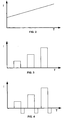
FIG. 2 is a chart of a direct current ramp for electroplating used in the present invention;
FIG. 3 is a chart of a forward pulse current ramp for electroplating used in the present invention;
FIG. 4 is a chart of a reverse pulse current ramp for electroplating used in the present invention; and
FIG. 5 is a simplified cross-section of a semiconductor wafer formed in accordance with the present invention.
BEST MODE FOR CARRYING OUT THE INVENTION
Referring now to FIG. 1A (PRIOR ART), therein is shown a plan view of a prior art pair of perpendicularly aligned semiconductor channels of a conductive material such as aluminum, copper, tungsten or polysilicon disposed over a production semiconductor wafer 100. A first channel 101 is shown disposed below a second channel 102 which extends substantially perpendicular to the first channel 101 in the plan view. Similarly, a round via 104 connects the first and second channels 101 and 102 and is a part of the second channel 102. The first channel comprises a first conductive material. The second channel 102 is formed by filling a second channel opening 106 disposed in a second channel oxide layer 108 with a second conductive material. The second channel opening 106 is defined by walls (sidewalls) 109 of second oxide layer 108.
Referring now to FIG. 1B (PRIOR ART), therein is shown a cross-section of FIG. 1A (PRIOR ART) along 1B—1B. The first channel 101 is disposed over a polysilicon gate 110 and a dielectric 112 of a semiconductor device on an integrated circuit chip (not shown). The first and second channels 101 and 102 are in horizontal planes separated vertically by a stop nitride layer 114, a via oxide layer 116, and a thin via nitride layer 117. The cross-sectional area of the round via 104 of FIG. 1A (PRIOR ART) defines a cylindrical via 120 when it is filled with the second conductive material.
Also shown disposed around the first channel 101 are an adhesion/barrier layer 121 and seed layer 122, and around the second channel 102 and the cylindrical via 120 is an adhesion/barrier layer 123 and seed layer 124. The adhesion/barrier layers include adhesion/barrier material combinations such as titanium/titanium nitride, tantalum/tantalum nitride, and tungsten nitride for copper seed layers and copper or copper alloy conductive materials.
In electroplating semiconductors, the semiconductor wafer 100 would be placed in an electroplating bath having a solution of the conductive material ions, and the seed layer 124 would be used as an electrode for the conductive material to be deposited upon. In the past, a number of different ways of applying the plating current were used. Three approaches were direct current, forward pulse current, and reverse pulse current. The power levels of these approaches were generally constant with the compromise being made between trying to obtain a fine grain size of the deposited material versus the time the process took. Therefore, the usual procedure was to seek the fastest electroplating time which would still permit fine enough grain size to meet certain electro-migration life expectancies.
Referring now to FIG. 2, therein is shown a chart of the direct current ramp for electroplating. Initially, the direct current is started at a low flow rate to cause the conductive material to be deposited with a very fine grain size. This maximizes resistance to electro-migration. Since these fine grain sizes are achieved near the surface of the seed layer 124, excellent adhesion is achieved which also promotes good electro-migration resistance. Further, since the vias are smaller than the channels, the vias tend to fill first with fine grain size conductive material.
Subsequently, the current level is increased to as to cause the formation of larger grain sizes which more quickly fill up the channels.
Referring now to FIG. 3, therein is shown a chart of a forward pulse current ramp. While it is understood that forward pulse current applies a large number of pulses, three pulses are shown to demonstrate the increasing amount of forward pulse current being applied. The forward pulse current approach allows for better circulation of conductive material ions to the seed layer during electro-deposition.
Referring now to FIG. 4, therein is shown a chart of a reverse pulse current ramp. As would be understood in the process there are many forward and reverse pulses, but three are shown for convenience. Again, the gradually increasing current impulses are shown with the reverse pulses in-between. This process circulates the material ions even better than just a strict forward pulse process and thus allows even faster plating.
Referring now to FIG. 5, therein is shown the cross-section of a semiconductor wafer 200 with a pair of perpendicularly aligned semiconductor channels, disposed over a silicon substrate 110 formed in accordance with the present invention. For convenience of illustration, like reference numerals are used in FIG. 5 to denote like elements already described in FIG. 1A (PRIOR ART) through FIG. 1C (PRIOR ART). Similarly, for purposes of clarity, the adhesion/barrier layer 123, seed layer 122, adhesion/barrier layer 121, polysilicon gate 110 and dielectric 112 are not shown.
At this stage, the seed layer 124 is shown formed in the second channel opening 106 and the via 118. In the via 118 are shown fine grain size 210, 220, 230, 240, and 250. The grain boundaries, such as between conductive materials 210 and 220, help prevent the electro-migration of the conductive material from the conductive channel 201 through to the conductive channel 106. These fine grain sizes are deposited at the lower current densities which are applied for longer periods of time.
As the plating process is speeded up using higher current densities, the grain sizes start to increase in size as shown by the larger grain conductive material 260, 270, 280, 290, and 300.
As would be evident to those skilled in the art, any time lost by the deposition of the fine grain size conductive material would be more than compensated for by the speed at which the large grain size conductive material could be deposited. Thus, there would be a significant increase in the throughput of the ramped current density approach of the current invention.
In production, a conventional first damascene process was used to dispose a first channel 201 in a first channel oxide layer (not shown) above portions of a semiconductor device (not shown) on a production semiconductor wafer 200. The damascene process is a photolithographic process which uses a mask to define a first channel opening (not shown) in the first channel oxide layer. The first channel opening is then filled with a adhesion/barrier layer, a seed layer, and a first conductive material, such as copper, to form the first channel 201 using the ramped current density electroplating technique of the present invention. The stop nitride layer 114, the via oxide layer 116, and the via nitride layer 117 would be successively deposited on top of the first channel 201 and the first channel oxide layer using conventional deposition technique.
By using the via photoresist and the via photolithographic process followed by nitride etching of a round via 104 in the via nitride layer 117, the basis for the cylindrical via 118 was formed. The subsequent deposition of the second channel oxide layer 108 prepares the way for the second channel 106 to be perpendicular to the first channel 201.
The second damascene process uses a further mask to define the second channel opening 106 in the second channel oxide layer 108. Since the second damascene process uses an anisotropic oxide etch, the etch also forms the cylindrical via 118 down to the stop nitride layer 114. The anisotropic oxide etch etches faster in the vertical direction of FIG. 5 than in the horizontal direction. The nitride etch of the stop nitride layer 114 exposes a portion of the first channel 201 and completes the etching steps.
Next, a thin adhesion/barrier layer (not shown) is deposited in the second channel opening 106 and the cylindrical via 118, including along the walls of the second channel opening 106 and the cylindrical via 118. The thickness of the adhesion/barrier material is insufficient to fill the second channel opening 106 and the cylindrical via 118. Examples of suitable adhesion/barrier materials include refractory combinations as titanium/titanium nitride, tantalum/tantalum nitride, and tungsten nitride. The adhesion/barrier layer is deposited using conventional deposition techniques, such as physical vapor deposition, chemical vapor deposition, or a combination thereof.
Thereafter, the thin seed layer 124 is deposited on the adhesion/barrier layer in the second channel opening 106 and the cylindrical via 118. Again, the thickness of the seed layer 124 is insufficient to fill the second channel opening 106 and the cylindrical via 118. Examples of suitable seed materials include copper and copper alloys. The seed layer 224 is deposited using a conventional metal deposition technique such as ion metal plasma (IMP), hollow cathode metalization (HCM), combinations of them with electroplating, or electroless deposition. In these processes, the metal ions are charged and directed toward the silicon wafer 200 to be deposited.
Next, the second conductive material is deposited into second channel opening 106 and via 118 on top of the seed layer 224 using the ramped current density electroplating technique. Thereafter, a chemical mechanical polishing process is used to complete the conventional connection process similar to what were shown and described in FIGS. 1A and 1B.
While the best mode utilizes copper as the conductive material, it should be understood that the present invention is applicable to other conductive and electroplating materials such as aluminum, copper, gold, silver, an alloy thereof, and a combination thereof.
Further, although the embodiments of the present invention are directed to using the dual damascene technique, it also will be recognized by those skilled in the art that other techniques of forming interconnects or other traditional techniques of forming low resistance contacts or plugs which involve filling an opening with conductive materials such as tungsten or aluminum may be used to practice the present invention. In addition, while the embodiments of the present inventions form a seed layer in a channel opening and a via atop another conductive channel, it should be understood that the present invention is applicable to forming a seed layer in a channel opening and/or a via atop a conductive or a doped region formed on a semiconductor substrate.
While the invention has been described in conjunction with a specific best mode, it is to be understood that many alternatives, modifications, and variations will be apparent to those skilled in the art in light of the aforegoing description. Accordingly, it is intended to embrace all such alternatives, modifications, and variations which fall within the spirit and scope of the included claims. All matters set forth herein or shown in the accompanying drawings are to be interpreted in an illustrative and non-limiting sense.

Claims (5)

The invention claimed is:
1. A semiconductor device comprising:
a silicon substrate;
a dielectric disposed on said silicon substrate, said dielectric having an opening provided therein;
a seed layer disposed in and lining said opening in said dielectric; and
a conductive layer disposed in said seed layer, said conductive material having fine grain size conductive material proximate said seed layer and large grain size conductive material distal therefrom, and said conductive material is deposited by a ramped pulsed current density plating process.
2. The semiconductor device as claimed in claim 1 including;
a further dielectric layer disposed thereon, said further dielectric layer having channels and vias provided therein, said vias in contact with said conductive material in said dielectric;
a further seed layer disposed in said channels and vias provided in said further dielectric layer; and
further conductive material disposed in said further seed layer, said further conductive material having smaller grain size conductive material inside said via than in said channel.
3. The semiconductor device as claimed in claim 1 wherein said conductive material is selected from a group comprising aluminum, copper, gold, silver, an alloy thereof, and a combination thereof.
4. The semiconductor device as claimed in claim 1 wherein said conductive material is copper.
5. The semiconductor device as claimed in claim 1 wherein said conductive material is deposited by a ramped current density electroplating process.
US09/975,032 1999-03-26 2001-10-10 Variable grain size in conductors for semiconductor vias and trenches Expired - Fee Related US6489683B1 (en)

Priority Applications (1)

Application Number Priority Date Filing Date Title
US09/975,032 US6489683B1 (en) 1999-03-26 2001-10-10 Variable grain size in conductors for semiconductor vias and trenches

Applications Claiming Priority (2)

Application Number Priority Date Filing Date Title
US09/276,839 US6340633B1 (en) 1999-03-26 1999-03-26 Method for ramped current density plating of semiconductor vias and trenches
US09/975,032 US6489683B1 (en) 1999-03-26 2001-10-10 Variable grain size in conductors for semiconductor vias and trenches

Related Parent Applications (1)

Application Number Title Priority Date Filing Date
US09/276,839 Division US6340633B1 (en) 1999-03-26 1999-03-26 Method for ramped current density plating of semiconductor vias and trenches

Publications (1)

Publication Number Publication Date
US6489683B1 true US6489683B1 (en) 2002-12-03

Family

ID=23058272

Family Applications (2)

Application Number Title Priority Date Filing Date
US09/276,839 Expired - Lifetime US6340633B1 (en) 1999-03-26 1999-03-26 Method for ramped current density plating of semiconductor vias and trenches
US09/975,032 Expired - Fee Related US6489683B1 (en) 1999-03-26 2001-10-10 Variable grain size in conductors for semiconductor vias and trenches

Family Applications Before (1)

Application Number Title Priority Date Filing Date
US09/276,839 Expired - Lifetime US6340633B1 (en) 1999-03-26 1999-03-26 Method for ramped current density plating of semiconductor vias and trenches

Country Status (1)

Country Link
US (2) US6340633B1 (en)

Cited By (2)

* Cited by examiner, † Cited by third party
Publication number Priority date Publication date Assignee Title
US7090928B2 (en) 2003-04-01 2006-08-15 The University Of Southern California Binuclear compounds
US20090057159A1 (en) * 2005-06-07 2009-03-05 Massachusetts Institute Of Technology Method for producing alloy deposits and controlling the nanostructure thereof using negative current pulsing electro-deposition

Families Citing this family (21)

* Cited by examiner, † Cited by third party
Publication number Priority date Publication date Assignee Title
WO2001084617A1 (en) * 2000-04-27 2001-11-08 Nu Tool Inc. Conductive structure for use in multi-level metallization and process
US6913680B1 (en) 2000-05-02 2005-07-05 Applied Materials, Inc. Method of application of electrical biasing to enhance metal deposition
JP2004513221A (en) 2000-05-23 2004-04-30 アプライド マテリアルズ インコーポレイテッド Method and apparatus for overcoming copper seed layer anomalies and adjusting surface feature size and aspect ratio
EP1470268A2 (en) * 2000-10-03 2004-10-27 Applied Materials, Inc. Method and associated apparatus for tilting a substrate upon entry for metal deposition
US6432821B1 (en) * 2000-12-18 2002-08-13 Intel Corporation Method of copper electroplating
US6534865B1 (en) * 2001-06-12 2003-03-18 Advanced Micro Devices, Inc. Method of enhanced fill of vias and trenches
JP4000796B2 (en) * 2001-08-08 2007-10-31 株式会社豊田自動織機 Via hole copper plating method
US6689686B2 (en) * 2001-09-27 2004-02-10 Texas Instruments Incorporated System and method for electroplating fine geometries
US6911136B2 (en) * 2002-04-29 2005-06-28 Applied Materials, Inc. Method for regulating the electrical power applied to a substrate during an immersion process
US8002960B2 (en) * 2003-12-18 2011-08-23 Dyesol Ltd. Method for electrolytic engineering of nano-particulate layers
US20060175201A1 (en) * 2005-02-07 2006-08-10 Hooman Hafezi Immersion process for electroplating applications
US7368379B2 (en) * 2005-08-04 2008-05-06 Taiwan Semiconductor Manufacturing Company, Ltd. Multi-layer interconnect structure for semiconductor devices
US7850836B2 (en) * 2005-11-09 2010-12-14 Nanyang Technological University Method of electro-depositing a conductive material in at least one through-hole via of a semiconductor substrate
EP1860210A1 (en) * 2006-05-22 2007-11-28 Siemens Aktiengesellschaft Method for electrolytic treatment of a workpiece
JP4397399B2 (en) 2007-02-15 2010-01-13 富士通株式会社 Manufacturing method of semiconductor device
US20080283404A1 (en) * 2007-05-14 2008-11-20 Nec Electronics Corporation Method of manufacturing semiconductor device to decrease defect number of plating film
EP2312641A1 (en) * 2009-10-13 2011-04-20 Ecole Polytechnique Fédérale de Lausanne (EPFL) Device comprising electrical contacts and its production process
JP2011204750A (en) * 2010-03-24 2011-10-13 Elpida Memory Inc Method of manufacturing semiconductor device
US8617982B2 (en) * 2010-10-05 2013-12-31 Novellus Systems, Inc. Subtractive patterning to define circuit components
US8877632B1 (en) * 2013-05-13 2014-11-04 Intel Corporation Providing a void-free filled interconnect structure in a layer of package substrate
US9899234B2 (en) 2014-06-30 2018-02-20 Lam Research Corporation Liner and barrier applications for subtractive metal integration

Citations (7)

* Cited by examiner, † Cited by third party
Publication number Priority date Publication date Assignee Title
US3876389A (en) * 1970-06-30 1975-04-08 Ibm Composite material, inclusions thereof, and method therefor
US5906725A (en) * 1997-06-23 1999-05-25 Industrial Technology Research Institute Method for preparing nickel-zinc-copper or nickel-zinc alloy electroplating solutions from zinc-containing waste articles having a nickel/copper electroplating layer
US5972192A (en) * 1997-07-23 1999-10-26 Advanced Micro Devices, Inc. Pulse electroplating copper or copper alloys
US6024857A (en) * 1997-10-08 2000-02-15 Novellus Systems, Inc. Electroplating additive for filling sub-micron features
US6074544A (en) * 1998-07-22 2000-06-13 Novellus Systems, Inc. Method of electroplating semiconductor wafer using variable currents and mass transfer to obtain uniform plated layer
US6242349B1 (en) * 1998-12-09 2001-06-05 Advanced Micro Devices, Inc. Method of forming copper/copper alloy interconnection with reduced electromigration
US6297157B1 (en) * 1999-11-01 2001-10-02 Advanced Micro Devices, Inc. Time ramped method for plating of high aspect ratio semiconductor vias and channels

Family Cites Families (17)

* Cited by examiner, † Cited by third party
Publication number Priority date Publication date Assignee Title
US4140596A (en) * 1975-12-22 1979-02-20 Vereinigte Metallwerke Ranshofen-Berndorf Aktiengesellschaft Process for the electrolytic refining of copper
US4142947A (en) * 1977-05-12 1979-03-06 Uri Cohen Electrodeposition of polycrystalline silicon from a molten fluoride bath and product
JPS6043175B2 (en) * 1977-10-12 1985-09-26 株式会社日立製作所 Manufacturing method of metal catalyst
US4345107A (en) * 1979-06-18 1982-08-17 Ametek, Inc. Cadmium telluride photovoltaic cells
US4483752A (en) * 1982-09-28 1984-11-20 Eltech Systems Corporation Valve metal electrodeposition onto graphite
US4514265A (en) 1984-07-05 1985-04-30 Rca Corporation Bonding pads for semiconductor devices
US4685210A (en) * 1985-03-13 1987-08-11 The Boeing Company Multi-layer circuit board bonding method utilizing noble metal coated surfaces
US4869971A (en) 1986-05-22 1989-09-26 Nee Chin Cheng Multilayer pulsed-current electrodeposition process
US5326454A (en) 1987-08-26 1994-07-05 Martin Marietta Corporation Method of forming electrodeposited anti-reflective surface coatings
US5039381A (en) 1989-05-25 1991-08-13 Mullarkey Edward J Method of electroplating a precious metal on a semiconductor device, integrated circuit or the like
US5368711A (en) 1990-08-01 1994-11-29 Poris; Jaime Selective metal electrodeposition process and apparatus
JPH07273118A (en) * 1994-03-28 1995-10-20 Toshiba Corp Formation of wiring and electrode
US5662788A (en) * 1996-06-03 1997-09-02 Micron Technology, Inc. Method for forming a metallization layer
US5913147A (en) * 1997-01-21 1999-06-15 Advanced Micro Devices, Inc. Method for fabricating copper-aluminum metallization
US5933758A (en) * 1997-05-12 1999-08-03 Motorola, Inc. Method for preventing electroplating of copper on an exposed surface at the edge exclusion of a semiconductor wafer
US5969422A (en) * 1997-05-15 1999-10-19 Advanced Micro Devices, Inc. Plated copper interconnect structure
US5968333A (en) * 1998-04-07 1999-10-19 Advanced Micro Devices, Inc. Method of electroplating a copper or copper alloy interconnect

Patent Citations (7)

* Cited by examiner, † Cited by third party
Publication number Priority date Publication date Assignee Title
US3876389A (en) * 1970-06-30 1975-04-08 Ibm Composite material, inclusions thereof, and method therefor
US5906725A (en) * 1997-06-23 1999-05-25 Industrial Technology Research Institute Method for preparing nickel-zinc-copper or nickel-zinc alloy electroplating solutions from zinc-containing waste articles having a nickel/copper electroplating layer
US5972192A (en) * 1997-07-23 1999-10-26 Advanced Micro Devices, Inc. Pulse electroplating copper or copper alloys
US6024857A (en) * 1997-10-08 2000-02-15 Novellus Systems, Inc. Electroplating additive for filling sub-micron features
US6074544A (en) * 1998-07-22 2000-06-13 Novellus Systems, Inc. Method of electroplating semiconductor wafer using variable currents and mass transfer to obtain uniform plated layer
US6242349B1 (en) * 1998-12-09 2001-06-05 Advanced Micro Devices, Inc. Method of forming copper/copper alloy interconnection with reduced electromigration
US6297157B1 (en) * 1999-11-01 2001-10-02 Advanced Micro Devices, Inc. Time ramped method for plating of high aspect ratio semiconductor vias and channels

Cited By (5)

* Cited by examiner, † Cited by third party
Publication number Priority date Publication date Assignee Title
US7090928B2 (en) 2003-04-01 2006-08-15 The University Of Southern California Binuclear compounds
US20060269785A1 (en) * 2003-04-01 2006-11-30 Thompson Mark E Binuclear compounds
US7824778B2 (en) 2003-04-01 2010-11-02 The University Of Southern California Binuclear compounds
US20090057159A1 (en) * 2005-06-07 2009-03-05 Massachusetts Institute Of Technology Method for producing alloy deposits and controlling the nanostructure thereof using negative current pulsing electro-deposition
US8906216B2 (en) * 2005-06-07 2014-12-09 Massachusetts Institute Of Technology Method for producing alloy deposits and controlling the nanostructure thereof using electro-deposition with controlled polarity ratio

Also Published As

Publication number Publication date
US6340633B1 (en) 2002-01-22

Similar Documents

Publication Publication Date Title
US6489683B1 (en) Variable grain size in conductors for semiconductor vias and trenches
US6239021B1 (en) Dual barrier and conductor deposition in a dual damascene process for semiconductors
US6479902B1 (en) Semiconductor catalytic layer and atomic layer deposition thereof
US6228754B1 (en) Method for forming semiconductor seed layers by inert gas sputter etching
US6144099A (en) Semiconductor metalization barrier
US6174799B1 (en) Graded compound seed layers for semiconductors
US6440289B1 (en) Method for improving seed layer electroplating for semiconductor
US6509267B1 (en) Method of forming low resistance barrier on low k interconnect with electrolessly plated copper seed layer
US6734559B1 (en) Self-aligned semiconductor interconnect barrier and manufacturing method therefor
US6417094B1 (en) Dual-damascene interconnect structures and methods of fabricating same
US6657304B1 (en) Conformal barrier liner in an integrated circuit interconnect
US6297157B1 (en) Time ramped method for plating of high aspect ratio semiconductor vias and channels
US6232230B1 (en) Semiconductor interconnect interface processing by high temperature deposition
US6534865B1 (en) Method of enhanced fill of vias and trenches
EP1048056A1 (en) A single step electroplating process for interconnect via fill and metal line patterning
US6143650A (en) Semiconductor interconnect interface processing by pulse laser anneal
US6187670B1 (en) Multi-stage method for forming optimized semiconductor seed layers
US8084355B2 (en) Methods of forming copper-comprising conductive lines in the fabrication of integrated circuitry
US6261946B1 (en) Method for forming semiconductor seed layers by high bias deposition
US8053894B2 (en) Surface treatment of metal interconnect lines
US6146993A (en) Method for forming in-situ implanted semiconductor barrier layers
US6320263B1 (en) Semiconductor metalization barrier and manufacturing method therefor
US6368965B1 (en) Method for low stress plating of semiconductor vias and channels
US6150268A (en) Barrier materials for metal interconnect
US6531780B1 (en) Via formation in integrated circuit interconnects

Legal Events

Date Code Title Description
FPAY Fee payment

Year of fee payment: 4

AS Assignment

Owner name: GLOBALFOUNDRIES INC., CAYMAN ISLANDS

Free format text: AFFIRMATION OF PATENT ASSIGNMENT;ASSIGNOR:ADVANCED MICRO DEVICES, INC.;REEL/FRAME:023119/0083

Effective date: 20090630

FPAY Fee payment

Year of fee payment: 8

REMI Maintenance fee reminder mailed
LAPS Lapse for failure to pay maintenance fees
STCH Information on status: patent discontinuation

Free format text: PATENT EXPIRED DUE TO NONPAYMENT OF MAINTENANCE FEES UNDER 37 CFR 1.362

FP Lapsed due to failure to pay maintenance fee

Effective date: 20141203

AS Assignment

Owner name: GLOBALFOUNDRIES U.S. INC., NEW YORK

Free format text: RELEASE BY SECURED PARTY;ASSIGNOR:WILMINGTON TRUST, NATIONAL ASSOCIATION;REEL/FRAME:056987/0001

Effective date: 20201117