US6495477B2 - Method for forming a nitridized interface on a semiconductor substrate - Google Patents

Method for forming a nitridized interface on a semiconductor substrate Download PDF

Info

Publication number
US6495477B2
US6495477B2 US09/862,348 US86234801A US6495477B2 US 6495477 B2 US6495477 B2 US 6495477B2 US 86234801 A US86234801 A US 86234801A US 6495477 B2 US6495477 B2 US 6495477B2
Authority
US
United States
Prior art keywords
fluorine
doped
nitridized
substrate
undoped
Prior art date
Legal status (The legal status is an assumption and is not a legal conclusion. Google has not performed a legal analysis and makes no representation as to the accuracy of the status listed.)
Expired - Fee Related
Application number
US09/862,348
Other versions
US20010044222A1 (en
Inventor
Jonathan J. Taylor
David F. Jendresky
Current Assignee (The listed assignees may be inaccurate. Google has not performed a legal analysis and makes no representation or warranty as to the accuracy of the list.)
Samsung Austin Semiconductor LLC
Original Assignee
Samsung Austin Semiconductor LLC
Priority date (The priority date is an assumption and is not a legal conclusion. Google has not performed a legal analysis and makes no representation as to the accuracy of the date listed.)
Filing date
Publication date
Application filed by Samsung Austin Semiconductor LLC filed Critical Samsung Austin Semiconductor LLC
Priority to US09/862,348 priority Critical patent/US6495477B2/en
Publication of US20010044222A1 publication Critical patent/US20010044222A1/en
Application granted granted Critical
Publication of US6495477B2 publication Critical patent/US6495477B2/en
Anticipated expiration legal-status Critical
Expired - Fee Related legal-status Critical Current

Links

Images

Classifications

    • HELECTRICITY
    • H01ELECTRIC ELEMENTS
    • H01LSEMICONDUCTOR DEVICES NOT COVERED BY CLASS H10
    • H01L21/00Processes or apparatus adapted for the manufacture or treatment of semiconductor or solid state devices or of parts thereof
    • H01L21/02Manufacture or treatment of semiconductor devices or of parts thereof
    • H01L21/02104Forming layers
    • H01L21/02107Forming insulating materials on a substrate
    • H01L21/02109Forming insulating materials on a substrate characterised by the type of layer, e.g. type of material, porous/non-porous, pre-cursors, mixtures or laminates
    • H01L21/02112Forming insulating materials on a substrate characterised by the type of layer, e.g. type of material, porous/non-porous, pre-cursors, mixtures or laminates characterised by the material of the layer
    • H01L21/02123Forming insulating materials on a substrate characterised by the type of layer, e.g. type of material, porous/non-porous, pre-cursors, mixtures or laminates characterised by the material of the layer the material containing silicon
    • H01L21/0217Forming insulating materials on a substrate characterised by the type of layer, e.g. type of material, porous/non-porous, pre-cursors, mixtures or laminates characterised by the material of the layer the material containing silicon the material being a silicon nitride not containing oxygen, e.g. SixNy or SixByNz
    • HELECTRICITY
    • H01ELECTRIC ELEMENTS
    • H01LSEMICONDUCTOR DEVICES NOT COVERED BY CLASS H10
    • H01L21/00Processes or apparatus adapted for the manufacture or treatment of semiconductor or solid state devices or of parts thereof
    • H01L21/70Manufacture or treatment of devices consisting of a plurality of solid state components formed in or on a common substrate or of parts thereof; Manufacture of integrated circuit devices or of parts thereof
    • H01L21/71Manufacture of specific parts of devices defined in group H01L21/70
    • H01L21/76Making of isolation regions between components
    • CCHEMISTRY; METALLURGY
    • C23COATING METALLIC MATERIAL; COATING MATERIAL WITH METALLIC MATERIAL; CHEMICAL SURFACE TREATMENT; DIFFUSION TREATMENT OF METALLIC MATERIAL; COATING BY VACUUM EVAPORATION, BY SPUTTERING, BY ION IMPLANTATION OR BY CHEMICAL VAPOUR DEPOSITION, IN GENERAL; INHIBITING CORROSION OF METALLIC MATERIAL OR INCRUSTATION IN GENERAL
    • C23CCOATING METALLIC MATERIAL; COATING MATERIAL WITH METALLIC MATERIAL; SURFACE TREATMENT OF METALLIC MATERIAL BY DIFFUSION INTO THE SURFACE, BY CHEMICAL CONVERSION OR SUBSTITUTION; COATING BY VACUUM EVAPORATION, BY SPUTTERING, BY ION IMPLANTATION OR BY CHEMICAL VAPOUR DEPOSITION, IN GENERAL
    • C23C28/00Coating for obtaining at least two superposed coatings either by methods not provided for in a single one of groups C23C2/00 - C23C26/00 or by combinations of methods provided for in subclasses C23C and C25C or C25D
    • CCHEMISTRY; METALLURGY
    • C23COATING METALLIC MATERIAL; COATING MATERIAL WITH METALLIC MATERIAL; CHEMICAL SURFACE TREATMENT; DIFFUSION TREATMENT OF METALLIC MATERIAL; COATING BY VACUUM EVAPORATION, BY SPUTTERING, BY ION IMPLANTATION OR BY CHEMICAL VAPOUR DEPOSITION, IN GENERAL; INHIBITING CORROSION OF METALLIC MATERIAL OR INCRUSTATION IN GENERAL
    • C23CCOATING METALLIC MATERIAL; COATING MATERIAL WITH METALLIC MATERIAL; SURFACE TREATMENT OF METALLIC MATERIAL BY DIFFUSION INTO THE SURFACE, BY CHEMICAL CONVERSION OR SUBSTITUTION; COATING BY VACUUM EVAPORATION, BY SPUTTERING, BY ION IMPLANTATION OR BY CHEMICAL VAPOUR DEPOSITION, IN GENERAL
    • C23C8/00Solid state diffusion of only non-metal elements into metallic material surfaces; Chemical surface treatment of metallic material by reaction of the surface with a reactive gas, leaving reaction products of surface material in the coating, e.g. conversion coatings, passivation of metals
    • C23C8/06Solid state diffusion of only non-metal elements into metallic material surfaces; Chemical surface treatment of metallic material by reaction of the surface with a reactive gas, leaving reaction products of surface material in the coating, e.g. conversion coatings, passivation of metals using gases
    • C23C8/28Solid state diffusion of only non-metal elements into metallic material surfaces; Chemical surface treatment of metallic material by reaction of the surface with a reactive gas, leaving reaction products of surface material in the coating, e.g. conversion coatings, passivation of metals using gases more than one element being applied in one step
    • CCHEMISTRY; METALLURGY
    • C23COATING METALLIC MATERIAL; COATING MATERIAL WITH METALLIC MATERIAL; CHEMICAL SURFACE TREATMENT; DIFFUSION TREATMENT OF METALLIC MATERIAL; COATING BY VACUUM EVAPORATION, BY SPUTTERING, BY ION IMPLANTATION OR BY CHEMICAL VAPOUR DEPOSITION, IN GENERAL; INHIBITING CORROSION OF METALLIC MATERIAL OR INCRUSTATION IN GENERAL
    • C23CCOATING METALLIC MATERIAL; COATING MATERIAL WITH METALLIC MATERIAL; SURFACE TREATMENT OF METALLIC MATERIAL BY DIFFUSION INTO THE SURFACE, BY CHEMICAL CONVERSION OR SUBSTITUTION; COATING BY VACUUM EVAPORATION, BY SPUTTERING, BY ION IMPLANTATION OR BY CHEMICAL VAPOUR DEPOSITION, IN GENERAL
    • C23C8/00Solid state diffusion of only non-metal elements into metallic material surfaces; Chemical surface treatment of metallic material by reaction of the surface with a reactive gas, leaving reaction products of surface material in the coating, e.g. conversion coatings, passivation of metals
    • C23C8/06Solid state diffusion of only non-metal elements into metallic material surfaces; Chemical surface treatment of metallic material by reaction of the surface with a reactive gas, leaving reaction products of surface material in the coating, e.g. conversion coatings, passivation of metals using gases
    • C23C8/36Solid state diffusion of only non-metal elements into metallic material surfaces; Chemical surface treatment of metallic material by reaction of the surface with a reactive gas, leaving reaction products of surface material in the coating, e.g. conversion coatings, passivation of metals using gases using ionised gases, e.g. ionitriding
    • HELECTRICITY
    • H01ELECTRIC ELEMENTS
    • H01LSEMICONDUCTOR DEVICES NOT COVERED BY CLASS H10
    • H01L21/00Processes or apparatus adapted for the manufacture or treatment of semiconductor or solid state devices or of parts thereof
    • H01L21/02Manufacture or treatment of semiconductor devices or of parts thereof
    • H01L21/02104Forming layers
    • H01L21/02107Forming insulating materials on a substrate
    • H01L21/02225Forming insulating materials on a substrate characterised by the process for the formation of the insulating layer
    • H01L21/02227Forming insulating materials on a substrate characterised by the process for the formation of the insulating layer formation by a process other than a deposition process
    • H01L21/02247Forming insulating materials on a substrate characterised by the process for the formation of the insulating layer formation by a process other than a deposition process formation by nitridation, e.g. nitridation of the substrate
    • HELECTRICITY
    • H01ELECTRIC ELEMENTS
    • H01LSEMICONDUCTOR DEVICES NOT COVERED BY CLASS H10
    • H01L21/00Processes or apparatus adapted for the manufacture or treatment of semiconductor or solid state devices or of parts thereof
    • H01L21/02Manufacture or treatment of semiconductor devices or of parts thereof
    • H01L21/02104Forming layers
    • H01L21/02107Forming insulating materials on a substrate
    • H01L21/02225Forming insulating materials on a substrate characterised by the process for the formation of the insulating layer
    • H01L21/02227Forming insulating materials on a substrate characterised by the process for the formation of the insulating layer formation by a process other than a deposition process
    • H01L21/02252Forming insulating materials on a substrate characterised by the process for the formation of the insulating layer formation by a process other than a deposition process formation by plasma treatment, e.g. plasma oxidation of the substrate
    • HELECTRICITY
    • H01ELECTRIC ELEMENTS
    • H01LSEMICONDUCTOR DEVICES NOT COVERED BY CLASS H10
    • H01L21/00Processes or apparatus adapted for the manufacture or treatment of semiconductor or solid state devices or of parts thereof
    • H01L21/02Manufacture or treatment of semiconductor devices or of parts thereof
    • H01L21/04Manufacture or treatment of semiconductor devices or of parts thereof the devices having at least one potential-jump barrier or surface barrier, e.g. PN junction, depletion layer or carrier concentration layer
    • H01L21/18Manufacture or treatment of semiconductor devices or of parts thereof the devices having at least one potential-jump barrier or surface barrier, e.g. PN junction, depletion layer or carrier concentration layer the devices having semiconductor bodies comprising elements of Group IV of the Periodic System or AIIIBV compounds with or without impurities, e.g. doping materials
    • H01L21/30Treatment of semiconductor bodies using processes or apparatus not provided for in groups H01L21/20 - H01L21/26
    • H01L21/31Treatment of semiconductor bodies using processes or apparatus not provided for in groups H01L21/20 - H01L21/26 to form insulating layers thereon, e.g. for masking or by using photolithographic techniques; After treatment of these layers; Selection of materials for these layers
    • H01L21/314Inorganic layers
    • H01L21/3143Inorganic layers composed of alternated layers or of mixtures of nitrides and oxides or of oxinitrides, e.g. formation of oxinitride by oxidation of nitride layers
    • HELECTRICITY
    • H01ELECTRIC ELEMENTS
    • H01LSEMICONDUCTOR DEVICES NOT COVERED BY CLASS H10
    • H01L21/00Processes or apparatus adapted for the manufacture or treatment of semiconductor or solid state devices or of parts thereof
    • H01L21/02Manufacture or treatment of semiconductor devices or of parts thereof
    • H01L21/04Manufacture or treatment of semiconductor devices or of parts thereof the devices having at least one potential-jump barrier or surface barrier, e.g. PN junction, depletion layer or carrier concentration layer
    • H01L21/18Manufacture or treatment of semiconductor devices or of parts thereof the devices having at least one potential-jump barrier or surface barrier, e.g. PN junction, depletion layer or carrier concentration layer the devices having semiconductor bodies comprising elements of Group IV of the Periodic System or AIIIBV compounds with or without impurities, e.g. doping materials
    • H01L21/30Treatment of semiconductor bodies using processes or apparatus not provided for in groups H01L21/20 - H01L21/26
    • H01L21/31Treatment of semiconductor bodies using processes or apparatus not provided for in groups H01L21/20 - H01L21/26 to form insulating layers thereon, e.g. for masking or by using photolithographic techniques; After treatment of these layers; Selection of materials for these layers
    • H01L21/314Inorganic layers
    • H01L21/316Inorganic layers composed of oxides or glassy oxides or oxide based glass
    • H01L21/31604Deposition from a gas or vapour
    • H01L21/31629Deposition of halogen doped silicon oxide, e.g. fluorine doped silicon oxide
    • HELECTRICITY
    • H01ELECTRIC ELEMENTS
    • H01LSEMICONDUCTOR DEVICES NOT COVERED BY CLASS H10
    • H01L21/00Processes or apparatus adapted for the manufacture or treatment of semiconductor or solid state devices or of parts thereof
    • H01L21/02Manufacture or treatment of semiconductor devices or of parts thereof
    • H01L21/04Manufacture or treatment of semiconductor devices or of parts thereof the devices having at least one potential-jump barrier or surface barrier, e.g. PN junction, depletion layer or carrier concentration layer
    • H01L21/18Manufacture or treatment of semiconductor devices or of parts thereof the devices having at least one potential-jump barrier or surface barrier, e.g. PN junction, depletion layer or carrier concentration layer the devices having semiconductor bodies comprising elements of Group IV of the Periodic System or AIIIBV compounds with or without impurities, e.g. doping materials
    • H01L21/30Treatment of semiconductor bodies using processes or apparatus not provided for in groups H01L21/20 - H01L21/26
    • H01L21/31Treatment of semiconductor bodies using processes or apparatus not provided for in groups H01L21/20 - H01L21/26 to form insulating layers thereon, e.g. for masking or by using photolithographic techniques; After treatment of these layers; Selection of materials for these layers
    • H01L21/314Inorganic layers
    • H01L21/318Inorganic layers composed of nitrides
    • H01L21/3185Inorganic layers composed of nitrides of siliconnitrides
    • HELECTRICITY
    • H01ELECTRIC ELEMENTS
    • H01LSEMICONDUCTOR DEVICES NOT COVERED BY CLASS H10
    • H01L21/00Processes or apparatus adapted for the manufacture or treatment of semiconductor or solid state devices or of parts thereof
    • H01L21/02Manufacture or treatment of semiconductor devices or of parts thereof
    • H01L21/04Manufacture or treatment of semiconductor devices or of parts thereof the devices having at least one potential-jump barrier or surface barrier, e.g. PN junction, depletion layer or carrier concentration layer
    • H01L21/18Manufacture or treatment of semiconductor devices or of parts thereof the devices having at least one potential-jump barrier or surface barrier, e.g. PN junction, depletion layer or carrier concentration layer the devices having semiconductor bodies comprising elements of Group IV of the Periodic System or AIIIBV compounds with or without impurities, e.g. doping materials
    • H01L21/30Treatment of semiconductor bodies using processes or apparatus not provided for in groups H01L21/20 - H01L21/26
    • H01L21/31Treatment of semiconductor bodies using processes or apparatus not provided for in groups H01L21/20 - H01L21/26 to form insulating layers thereon, e.g. for masking or by using photolithographic techniques; After treatment of these layers; Selection of materials for these layers
    • H01L21/3205Deposition of non-insulating-, e.g. conductive- or resistive-, layers on insulating layers; After-treatment of these layers
    • H01L21/321After treatment
    • H01L21/3211Nitridation of silicon-containing layers
    • HELECTRICITY
    • H01ELECTRIC ELEMENTS
    • H01LSEMICONDUCTOR DEVICES NOT COVERED BY CLASS H10
    • H01L21/00Processes or apparatus adapted for the manufacture or treatment of semiconductor or solid state devices or of parts thereof
    • H01L21/70Manufacture or treatment of devices consisting of a plurality of solid state components formed in or on a common substrate or of parts thereof; Manufacture of integrated circuit devices or of parts thereof
    • H01L21/71Manufacture of specific parts of devices defined in group H01L21/70
    • H01L21/76Making of isolation regions between components
    • H01L21/762Dielectric regions, e.g. EPIC dielectric isolation, LOCOS; Trench refilling techniques, SOI technology, use of channel stoppers
    • H01L21/76202Dielectric regions, e.g. EPIC dielectric isolation, LOCOS; Trench refilling techniques, SOI technology, use of channel stoppers using a local oxidation of silicon, e.g. LOCOS, SWAMI, SILO
    • HELECTRICITY
    • H01ELECTRIC ELEMENTS
    • H01LSEMICONDUCTOR DEVICES NOT COVERED BY CLASS H10
    • H01L21/00Processes or apparatus adapted for the manufacture or treatment of semiconductor or solid state devices or of parts thereof
    • H01L21/02Manufacture or treatment of semiconductor devices or of parts thereof
    • H01L21/04Manufacture or treatment of semiconductor devices or of parts thereof the devices having at least one potential-jump barrier or surface barrier, e.g. PN junction, depletion layer or carrier concentration layer
    • H01L21/18Manufacture or treatment of semiconductor devices or of parts thereof the devices having at least one potential-jump barrier or surface barrier, e.g. PN junction, depletion layer or carrier concentration layer the devices having semiconductor bodies comprising elements of Group IV of the Periodic System or AIIIBV compounds with or without impurities, e.g. doping materials
    • H01L21/30Treatment of semiconductor bodies using processes or apparatus not provided for in groups H01L21/20 - H01L21/26
    • H01L21/31Treatment of semiconductor bodies using processes or apparatus not provided for in groups H01L21/20 - H01L21/26 to form insulating layers thereon, e.g. for masking or by using photolithographic techniques; After treatment of these layers; Selection of materials for these layers
    • H01L21/314Inorganic layers
    • H01L21/316Inorganic layers composed of oxides or glassy oxides or oxide based glass
    • H01L21/3165Inorganic layers composed of oxides or glassy oxides or oxide based glass formed by oxidation
    • H01L21/31654Inorganic layers composed of oxides or glassy oxides or oxide based glass formed by oxidation of semiconductor materials, e.g. the body itself
    • H01L21/31658Inorganic layers composed of oxides or glassy oxides or oxide based glass formed by oxidation of semiconductor materials, e.g. the body itself by thermal oxidation, e.g. of SiGe
    • H01L21/31662Inorganic layers composed of oxides or glassy oxides or oxide based glass formed by oxidation of semiconductor materials, e.g. the body itself by thermal oxidation, e.g. of SiGe of silicon in uncombined form
    • HELECTRICITY
    • H01ELECTRIC ELEMENTS
    • H01LSEMICONDUCTOR DEVICES NOT COVERED BY CLASS H10
    • H01L21/00Processes or apparatus adapted for the manufacture or treatment of semiconductor or solid state devices or of parts thereof
    • H01L21/02Manufacture or treatment of semiconductor devices or of parts thereof
    • H01L21/04Manufacture or treatment of semiconductor devices or of parts thereof the devices having at least one potential-jump barrier or surface barrier, e.g. PN junction, depletion layer or carrier concentration layer
    • H01L21/18Manufacture or treatment of semiconductor devices or of parts thereof the devices having at least one potential-jump barrier or surface barrier, e.g. PN junction, depletion layer or carrier concentration layer the devices having semiconductor bodies comprising elements of Group IV of the Periodic System or AIIIBV compounds with or without impurities, e.g. doping materials
    • H01L21/30Treatment of semiconductor bodies using processes or apparatus not provided for in groups H01L21/20 - H01L21/26
    • H01L21/31Treatment of semiconductor bodies using processes or apparatus not provided for in groups H01L21/20 - H01L21/26 to form insulating layers thereon, e.g. for masking or by using photolithographic techniques; After treatment of these layers; Selection of materials for these layers
    • H01L21/32Treatment of semiconductor bodies using processes or apparatus not provided for in groups H01L21/20 - H01L21/26 to form insulating layers thereon, e.g. for masking or by using photolithographic techniques; After treatment of these layers; Selection of materials for these layers using masks

Definitions

  • This invention relates to a method for forming a nitridized interface on a substrate, and more particularly to improving uniformity of an ammonia plasma surface treatment on a semiconductor substrate. Specifically, this invention relates to forming a nitridized polysilicon interface using ammonia plasma doped with fluorine.
  • Silicon nitride films are commonly employed in the fabrication of circuits for use in modern semiconductor devices, such as the fabrication of metal-oxide semiconductor (“MOS”) devices for high density integrated circuits and submicron designs.
  • MOS metal-oxide semiconductor
  • silicon nitride films are employed in the manufacture of MOS devices using Local Oxidation of Silicon processes (“LOCOS”), as well as advanced LOCOS methods such as polysilicon buffered LOCOS processes (“PBLOCOS”). Further information on LOCOS-based processing technology may be found in Wolf.
  • LOCOS Local Oxidation of Silicon processes
  • PBLOCOS polysilicon buffered LOCOS processes
  • a pad of native oxide is typically formed on a semiconductor substrate for purposes of cushioning transition of stress between a silicon substrate and a silicon nitride film, which is deposited to serve as an oxidation mask.
  • Such pad oxides may be thermally-grown or deposited using chemical vapor deposition (“CVD”).
  • CVD chemical vapor deposition
  • a thin pad layer of thermally deposited silicon dioxide (SiO 2 ) in combination with a polysilicon buffer layer is formed.
  • PBLOCOS methods are typically utilized to enhance suppression of lateral oxidation and to provide a stress buffer layer between the oxide layer and a subsequently deposited silicon nitride layer.
  • silicon nitride and polysilicon buffer layers are removed selectively to expose those areas where field oxide growth is desired, leaving the active areas of the device covered.
  • Field oxide is then grown “locally” in the etched areas between the active areas covered by silicon nitride film to isolate them from each other. It is desirable to minimize the space required for these isolation zones, as they consume valuable semiconductor space.
  • first bird's beak when it extends into the substrate
  • second bird's beak when it occurs in the interface of the silicon nitride and polysilicon.
  • Bird's beak formation can change the active area size and potentially cause gate poly bridging.
  • First bird's beak areas consume additional space as they extend beyond the edges of the isolation zones, and work against the achievement of isolation requirements for submicron devices.
  • Second bird's beak areas tend to interfere with removal of polysilicon in a LOCOS-based process, leaving undesirable “stringers” of poly which may cause shorts and/or leakage.
  • the remainder of the silicon nitride layer and any buffer layer present underneath is typically removed in order that the active areas of the semiconductor device may be formed.
  • Substrate surfaces are typically nitridized using a CVD process such as ammonia-plasma CVD.
  • a CVD process such as ammonia-plasma CVD.
  • flow of reactant gasses, as well as reacted byproducts typically results in nonuniform film thickness.
  • Nonuniformity of treatment may be gauged or measured in terms of both film within wafer thickness nonuniformity, and in wafer to wafer nonuniformity. Film within wafer thickness nonuniformity may be expresses in terms of percentage standard deviation. Wafer to wafer nonuniformity typically averages from about 6 ⁇ to about 10 ⁇ .
  • Process capability is defined as the process spec width divided by (6 ⁇ ), and is typically expressed as C p or C pk .
  • FIG. 1 illustrates field oxide 18 formed on a semiconductor substrate 10 in isolation area 11 , using a conventional LOCOS-based process known in the art.
  • isolation area 11 is defined between active device areas 13 .
  • Active device areas 13 are covered by silicon dioxide pad layer 12 , polysilicon buffer layer 14 and silicon nitride layer 16 .
  • field oxide 18 extends into active areas 13 due to encroachment of oxide 18 into the substrate 10 , forming “first bird's beak” areas 17 , and between silicon nitride layer 16 and polysilicon buffer layer 14 , forming “second bird's beak” areas 19 .
  • polysilicon buffer layer 14 may remain between the “bird's beak” areas 17 and 19 , which tends to act as a mask against removal of polysilicon. These residual polysilicon areas are referred to as “poly stringers” and are undesirable due to their tendency to cause shorts and leakage.
  • a fluorine doped nitride surface treatment may be employed to form a fluorine-doped nitridized substrate interface.
  • Benefits of the disclosed method include, but are not limited to, reduction in nonuniformity of nitridized substrate surfaces and wafer to wafer nonuniformity, as well as the provision of a more stable process.
  • wafer yield may be increased over conventional undoped ammonia plasma treatment processes by, for example, substantially eliminating across-wafer nonuniformity and the presence of a “second bird's beak” in the field oxide edge areas formed in a LOCOS-based process.
  • process capability C p , C pk
  • Si—O—Si bonds are believed to be replaced by Si—F, non-bridging Si—O, and/or Si—N bonds. Formation of Si—N bonds is believed to be the predominate reaction, and it is believed that these bonds create a more uniform interface between a polysilicon layer and a subsequent silicon nitride layer.
  • fluorine is also believed to break Si—H bonds and Si—OH bonds which may form in NH 3 plasma, thus tending to form stronger Si—F bonds. It is believed that one or more of the previously described mechanisms retard lateral diffusion and reaction of oxygen during field oxide growth, thus yielding better uniformity.
  • a source of fluorine typically carbon hexafluorine, C 2 F 6 (Halocarbon-116)
  • a substrate surface such as oxide or polysilicon
  • LOCOS-based processes are known in the art and are described, for example, in Wolf, Stanley Silicon Processing for the VLSI Era, Volume 2 —Process Integration , Lattice Press, Sunset Beach, Calif., pp. 12-41, 1990, which is incorporated herein by reference.
  • C 2 F 6 gas (typically employed as an etchant) is introduced into an ammonia plasma during nitride surface treatment of polysilicon.
  • fluorine-based dopant may surprisingly be used to reduce film within wafer thickness nonuniformity to less than or equal to about 2 ⁇ (or about 1 ⁇ ), as measured on a test wafer, resulting in reduction in wafer to wafer nonuniformity and providing a more stable process.
  • the disclosed method may be realized in any semiconductor fabrication surface treatment process employing silicon nitride.
  • the disclosed method may be employed in the manufacture of MOS semiconductor devices on a silicon substrate including, but not limited to, manufacture of DRAM devices.
  • a method of nitridizing the surface of a semiconductor substrate including forming a fluorine-doped nitridized surface on an upper surface of the substrate, such that an interface is defined between the fluorine-doped nitridized surface and the substrate surface.
  • the forming may include exposing the substrate surface to a treatment gas including a fluorine component and a nitrogen component; such that the exposure results in the formation of a fluorine-doped nitridized surface having an interface with the substrate surface.
  • the substrate surface may include silicon dioxide or polysilicon.
  • the nitrogen component may be at least one of ammonia, nitrogen, or a mixture thereof; the fluorine component may be at least one of C 2 H 6 , C 3 F 8 , CF 4 , or a mixture thereof; and the exposing may occur in a chemical vapor deposition process.
  • the nitrogen component may be ammonia; the fluorine component may be carbon hexafluorine; and the exposing may occur in a low pressure plasma enhanced chemical vapor deposition process.
  • the fluorine-doped nitridized surface may include a film may have a thickness of at least about 1 ⁇ to about is 40 ⁇ , alternatively from about 10 ⁇ to about 30 ⁇ .
  • the fluorine-doped nitridized surface may be formed using a treatment gas including a volume ratio of carbonhexafluorine to ammonia of from about 1:1 to about 1:20.
  • the method may further include exposing the fluorine-doped nitridized surface to an undoped treatment gas including a nitrogen component; such that the exposure results in the formation of an undoped nitridized surface on the fluorine-doped nitridized surface.
  • the nitrogen component of the fluorine doped treatment gas may be ammonia
  • the fluorine component of the fluorine-doped treatment gas may be carbon hexafluorine
  • the nitrogen component of the undoped treatment gas may be ammonia
  • the exposing to the fluorine-doped treatment gas and the exposing to the undoped treatment gas each may occur in a respective low pressure plasma enhanced chemical vapor deposition process.
  • the fluorine-doped nitridized surface may include a film may have a thickness of from about 1 ⁇ to about 40 ⁇ ; and the undoped nitridized surface may include a film may have a thickness of from about 700 ⁇ to about 3000 ⁇ .
  • the substrate may include a semiconductor wafer, and an upper surface of the undoped nitridized surface may have a within wafer thickness variation of less than about 2 ⁇ .
  • MOS semiconductor devices such as DRAM memory devices
  • methods for forming localized field oxide during fabrication of such devices on a substrate having a silicon dioxide pad layer present on an upper surface of the substrate and a polysilicon buffer layer disposed on an upper surface of the silicon dioxide pad layer including forming a fluorine-doped nitridized surface on an upper surface of the polysilicon buffer layer; such that an interface is defined between the fluorine-doped nitridized surface and the upper surface of the polysilicon buffer layer; forming an undoped nitridized surface on the fluorine-doped nitridized surface, the undoped nitridized surface and the fluorine-doped nitridized surface together forming a silicon nitride layer; defining at least one active region pattern on the silicon nitride layer; removing the silicon nitride and the polysilicon buffer layers in an area outside the active region pattern; and forming a field oxide region in the area
  • the formation of a fluorine-doped nitridized surface may include exposing the upper surface of the polysilicon buffer layer to a treatment gas including a mixture of carbon hexafluorine and ammonia in a low pressure plasma enhanced chemical vapor deposition process.
  • the formation of an undoped nitridized surface may include exposing the fluorine-doped nitridized surface to a treatment gas including ammonia and substantially no fluorine component in a low pressure plasma enhanced chemical vapor deposition process.
  • the fluorine-doped nitridized surface may include a film may have a thickness of at least about 10 ⁇ to about 30 ⁇ , alternatively from about 20 ⁇ to about 25 ⁇ .
  • the undoped nitridized surface may have a thickness of from about 700 ⁇ to about 3000 ⁇ , alternatively from about 1200 ⁇ to about 1800 ⁇ .
  • the fluorine-doped nitridized surface may be formed using a treatment gas including a volume ratio of carbonhexafluorine to ammonia of from about 1:3 to about 1:20.
  • the substrate may include a semiconductor wafer, and an upper surface of the undoped silicon nitride layer may have a within wafer thickness variation of less than about 2 ⁇ . In one embodiment, encroachment of oxide into the interface defined between the fluorine-doped nitridized surface and the upper surface of the polysilicon buffer layer may be inhibited or substantially prevented during formation of the field oxide region.
  • MOS semiconductor devices such as DRAM memory devices
  • methods for forming localized field oxide during fabrication of such devices on a silicon substrate including forming a pad layer of silicon dioxide on the silicon substrate; forming a buffer layer of polysilicon on the silicon dioxide pad layer, the pad layer of silicon dioxide being disposed between the buffer layer of polysilicon and the silicon substrate; forming a fluorine-doped nitridized surface on an upper surface of the polysilicon buffer layer; wherein an interface may be defined between the fluorine-doped nitridized surface and the upper surface of the polysilicon buffer layer; forming an undoped nitridized surface on the fluorine-doped nitridized surface, the undoped nitridized surface and the fluorine-doped nitridized surface together forming a silicon nitride layer; defining at least one active region pattern on the silicon nitride layer, removing the silicon nitride layer and the polysilicon buffer
  • Formation of a fluorine-doped nitridized surface may include exposing the upper surface of the polysilicon buffer layer to a treatment gas including a mixture of carbon hexafluorine and ammonia in a low pressure plasma enhanced chemical vapor deposition process; and formation of an undoped nitridized surface may include exposing the fluorine-doped nitridized surface to a treatment gas including ammonia and substantially no fluorine component in a low pressure plasma enhanced chemical vapor deposition process.
  • a fluorine-doped nitridized surface may include a film may have a thickness of from about 20 ⁇ to about 25 ⁇ , and/or an undoped nitridized surface may have a thickness of from about 1200 ⁇ to about 1800 ⁇ .
  • the fluorine-doped nitridized surface may be formed using a treatment gas including a volume ratio of carbonhexafluorine to ammonia of from about 1:3 to about 1:15.
  • an upper surface of the silicon nitride layer surface may have a within wafer thickness variation of less than about 2 ⁇ .
  • encroachment of oxide into the interface defined between the fluorine-doped nitridized surface and the upper surface of the polysilicon buffer layer may be inhibited or substantially prevented during the formation of the field oxide region.
  • FIG. 1 is a simplified partial cross-sectional view of a semiconductor substrate showing field oxide regions formed using a conventional LOCOS-based process, and exhibiting first and second “bird's beak” oxide encroachment beneath adjacent silicon nitride mask layers.
  • FIG. 2 is a simplified partial cross-sectional view of a semiconductor substrate with a pad oxide layer formed thereupon according to one embodiment of the disclosed method.
  • FIG. 3 is a simplified partial cross-sectional view of a semiconductor substrate with a pad oxide layer and polysilicon buffer layer formed thereupon according to one embodiment of the disclosed method.
  • FIG. 4 is a simplified partial cross-sectional view of a semiconductor substrate with a pad oxide layer, polysilicon buffer layer, fluorine-doped nitridized polysilicon interface and fluorine-doped silicon nitride film formed thereupon according to one embodiment of the disclosed method.
  • FIG. 5 is a simplified partial cross-sectional view of a semiconductor substrate with an oxide pad layer, polysilicon buffer layer, fluorine-doped nitridized polysilicon interface, fluorine-doped silicon nitride film and undoped silicon nitride film according to one embodiment of the disclosed method.
  • FIG. 6 is a simplified partial cross-sectional view of a semiconductor substrate of FIG. 5 with doped and undoped silicon nitride films and polysilicon buffer layers removed in preparation for forming field oxide regions according to one embodiment of the disclosed method.
  • FIG. 7 is a simplified partial cross-sectional view of a semiconductor substrate of FIG. 6 showing a field oxide region grown in the area where doped and undoped silicon nitride films and polysilicon buffer layers have been removed according to one embodiment of the disclosed method.
  • FIG. 8 is a simplified partial cross-sectional view of the semiconductor substrate of FIG. 7 showing doped and undoped silicon nitride films removed over the active areas of the semiconductor substrate according to one embodiment of the disclosed method.
  • FIG. 9 is a simplified partial cross-sectional view of the semiconductor substrate of FIG. 8 showing polysilicon buffer and oxide pad layers removed over the active areas of the semiconductor substrate according to one embodiment of the disclosed method.
  • FIG. 10 is a simplified schematic of a plasma-CVD reactor setup used in collecting data for Examples 1-4.
  • FIG. 11 is a contour map of silicon nitride film thickness for the wafer of slot 1 of Example 3.
  • FIG. 12 is a contour map of silicon nitride film thickness for the wafer of slot 3 of Example 3.
  • a fluorine-doped nitridized interface may be formed on a substrate surface using any method suitable for treating a substrate surface including, but not limited to, CVD.
  • fluorine-doped ammonia plasma may be used to treat a polysilicon surface using a CVD process.
  • any CVD-based method suitable for nitride surface treating may be employed including, but not limited to, plasma enhanced CVD (“PECVD”), non-plasma enhanced CVD, radiant energy CVD, low pressure CVD (“LPCVD”), atmospheric CVD, etc.
  • PECVD plasma enhanced CVD
  • LPCVD low pressure CVD
  • the term “CVD” also includes any possible combination of CVD types, for example, low pressure plasma enhanced chemical vapor deposition.
  • Suitable equipment includes any CVD equipment suitable for nitride surface treatment of substrate surfaces. Examples include, but are not limited to, commercially available from suppliers such as is Novellus, Applied Materials, Genus, etc. Particular examples include, but are not limited to, equipment available from Novellus (e.g., “CONCEPT II”), Applied Materials (e.g., “P5000”, “CENTURA”), and Matson.
  • Novellus e.g., “CONCEPT II”
  • Applied Materials e.g., “P5000”, “CENTURA”
  • Matson Matson
  • a fluorine-doped nitride surface treatment may be performed using any CVD treatment gas mixture suitable for supplying nitrogen and fluorine components to form a nitridized interface with a substrate surface.
  • suitable nitrogen gas components include, but are not limited to, at least one of ammonia, nitrogen, or a mixture thereof.
  • Suitable fluorine gas components include, but are not limited to, at least one of carbon hexafluorine (C 2 H 6 ), C 3 F 8 , carbon tetrafluoride (CF 4 ), or a mixture thereof.
  • uniformity of a nitride surface treatment may be improved by using a fluorine-doped ammonia plasma to form a fluorine-doped nitridized interface with a substrate surface.
  • Fluorine-doped ammonia plasma of the disclosed method may be advantageously employed in any semiconductor manufacturing method which utilizes ammonia plasma surface treatments.
  • fluorine-doped ammonia plasma may be employed in the manufacture of MOS devices such as logic devices, microprocessors or memory devices including DRAMs, SRAMs, and ROMs.
  • a fluorine-doped silicon nitride layer may be formed by a low pressure plasma enhanced chemical vapor deposition process using a treatment gas comprising a mixture of ammonia and carbon hexafluorine (C 2 H 6 , or “Halocarbon-116”).
  • Fluorine and nitrogen gas components may be present in a CVD treatment gas in any amount suitable for forming a fluorine-doped nitridized interface.
  • a volume ratio of carbon hexafluorine to ammonia of from about 1:1 to about 1:20, alternatively from about 1:3 to about 1:20, alternatively from about 1:3 to about 1:15, alternatively from about 1:5 to about 1:15, alternatively from about 1:7 to about 1:15, and further alternatively about 1:10, may be employed.
  • a treatment gas may optionally include other components if so desired.
  • any other CVD gas components known in the art to be suitable for use in the formation of silicon nitride films may be employed including, but not limited to, nitrogen.
  • nitrogen any other CVD gas components known in the art to be suitable for use in the formation of silicon nitride films
  • carbon hexafluorine and ammonia may be present in the ratios described above, with ammonia and other gas constituents, such as nitrogen, making up the remainder of the treatment gas volume.
  • An undoped second nitride surface treatment may be performed following creation of a fluorine-doped nitridized interface with a fluorine doped first nitride surface treatment.
  • an undoped nitride surface treatment may be performed using any suitable methods known in the art, including CVD methods described elsewhere herein.
  • “undoped” means containing substantially no fluorine atom content
  • “fluorine-doped” means containing sufficient fluorine atom content to result in or to form a nitridized interface with a substrate surface that inhibits or substantially prevents formation of a second bird's beak as described elsewhere herein.
  • a fluorine-doped nitridized interface may be formed on a substrate during a first nitride surface treatment by using a CVD treatment gas containing both fluorine and nitrogen components.
  • a fluorine component need only be of sufficient duration to create a fluorine-doped nitridized interface on a substrate surface that is capable of retarding or preventing lateral diffusion and reaction of oxygen at the nitridized interface during, for example, field oxide growth in a LOCOS-based process.
  • An undoped second nitride surface treatment may follow the first treatment, and may be performed using an undoped CVD treatment gas having a nitrogen component, such as ammonia.
  • such a second treatment is performed in a separate step, for example, in a separate reactor or in the same reactor after reconfiguration for processing with the undoped treatment gas mixture.
  • the fluorine component of the treatment gas may be shut off, with processing continuing with a treatment gas containing a nitrogen component.
  • a reactor system in which stoichiometrically correct amounts of treatment gas components may be supplied for both doped and undoped treatment steps.
  • Such a reactor system includes, for example, a Novellus “CONCEPT II”.
  • an associated fluorine-doped nitride film may be formed. It will be understood with benefit of this disclosure that as long as a fluorine-doped nitridized interface is formed on the surface, the thickness of an accompanying fluorine-doped nitride film may vary as desired.
  • overall thickness of a fluorine-doped nitride film layer formed on a polysilicon surface may be from about 1 ⁇ to about 40 ⁇ , alternatively from about 10 ⁇ to about 30 ⁇ , alternatively from about 20 ⁇ to about 25 ⁇ , and further alternatively about 23 ⁇ .
  • film thicknesses greater that about 40 ⁇ or less than about 1 ⁇ are also possible.
  • FIGS. 2-9 illustrate formation of field oxide on a substrate using one exemplary embodiment of the disclosed method in which a PBLOCOS process is employed with a fluorine doped nitride surface treatment of the polysilicon buffer layer.
  • a PBLOCOS process utilizing a polysilicon buffer layer is illustrated, it will be understood with benefit of the present disclosure that the benefit of a fluorine-doped nitride surface treatment may be realized when used in other processes and to when used to treat other substrate surfaces, for example, to treat a surface of a silicon dioxide layer in a LOCOS-based process.
  • a silicon dioxide pad layer 22 has been formed on substrate 20 .
  • Pad layer 22 may be formed to a desired thickness using any suitable method known in the art.
  • pad layer 22 may be thermally grown, or deposited by CVD.
  • pad layer 22 may have a thickness of from about 50 ⁇ to about 250 ⁇ , alternatively about 160 ⁇ , although thicknesses greater than about 250 ⁇ and less than about 50 ⁇ are also possible.
  • substrate means any semiconductor substrate including, but not limited to, a semiconductor wafer substrate such as silicon or GaAs. It will be understood that a “substrate” may include, among other things, a semiconductor wafer or a semiconductor wafer having various process layers formed on the wafer.
  • “layer” may be used interchangeably with “film”.
  • a polysilicon buffer layer 24 is shown deposited on pad oxide layer 22 .
  • Polysilicon buffer layer 24 may be formed using any suitable method known in the art using a CVD process.
  • buffer layer 24 may have a thickness of from about 200 ⁇ to about 1000 ⁇ , alternatively about 700 ⁇ , although thicknesses greater than about 200 ⁇ and less than about 1000 ⁇ are also possible.
  • polysilicon layer 24 has been exposed to a fluorine-doped nitride surface treatment, for example a low pressure fluorine-doped ammonia plasma CVD process, to form fluorine-doped nitridized polysilicon interface 25 .
  • fluorine-doped nitride film 26 has also been formed as a result of the surface treatment.
  • fluorine-doped film 26 may be formed to a thickness from about 1 ⁇ to about 40 ⁇ , alternatively from about 10 ⁇ to about 30 ⁇ , alternatively from about 20 ⁇ to about 25 ⁇ , and further alternatively about 23 ⁇ , using a treatment gas comprising a mixture of carbon hexafluorine and ammonia.
  • flow rate of carbon hexafluorine may be controlled to achieve a treatment gas having a relative volume or ratio of carbon hexafluorine to ammonia as described elsewhere herein.
  • flow rate of carbon hexafluorine may range from about 1 standard cubic centimeters per minute (sccm) to about 300 sccm, alternatively from about 20 sccm to about 200 sccm, alternatively from about 20 sccm to about 100 sccm, alternatively from about 20 to about 40 sccm, and further alternatively about 30 sccm; and simultaneous flow rate of ammonia may range from about 100 sccm to about 3000 sccm, alternatively from about 100 sccm to about 500 sccm, alternatively from about 200 sccm to about 400 sccm, and further alternatively about 300 sccm.
  • sccm standard cubic centimeters per minute
  • a conventional nitride surface treatment may be performed, either in a separate reactor and/or processing step, or in the same reactor by terminating flow of carbon hexafluorine.
  • conventional nitride surface treatment with undoped ammonia plasma results in formation of undoped silicon nitride film 28 on top of fluorine-doped nitride film 26 .
  • Thickness of film 28 may vary relative to film 26 as described elsewhere herein.
  • undoped nitride film 28 may be formed to a thickness of from about 700 ⁇ to about 3000 ⁇ , alternatively from about 1200 ⁇ to about 1800 ⁇ , and further alternatively about 1550 ⁇ .
  • active region patterns 42 may be defined on upper surface of silicon nitride layer 30 , typically using photoresist.
  • photoresist any photolithographic or other suitable method for forming a pattern of active device areas may be employed.
  • silicon nitride film layers 26 and 28 may be removed along with polysilicon buffer layer 24 , for example, by anisotropic etching to form field oxide area 40 between active areas 42 .
  • field oxide region 44 may be formed on substrate 20 within field oxide area 40 .
  • First “bird's beak” areas 46 are present at the surface of substrate 20 , but significantly, no second “bird's beak” exists.
  • Field oxide region 44 may be formed using any suitable method known in the art for forming field oxides, including a wet oxidation process, etc. In one embodiment, thickness of field oxide 44 may be from about 1000 ⁇ to about 10,000 ⁇ , alternatively from about 5000 ⁇ to about 9000 ⁇ .
  • film layers 28 and 26 may be removed in active areas 42 to expose polysilicon buffer layer 24 , for example, by chemical etching, HF acid stripping, reactive ion etching, etc.
  • polysilicon buffer layer 24 and oxide pad layer 22 may be removed in active areas 42 , for example, using a dry etching process in one or more steps so as to expose substrate 20 of active region 42 , as shown in FIG. 9 .
  • nonuniformity of nitridized substrate interfaces may be decreased, resulting in increased process capability.
  • film within wafer thickness nonuniformity (i.e., standard deviation/average wafer thickness) of a nitride treated polysilicon test wafer may be reduced to values as low as about 2% or less, from values of about 7% or more typically seen for surface treatments performed with conventional undoped ammonia plasma treatments.
  • Table 1 illustrates the difference in film uniformity (i.e., thickness variation) between a standard undoped silicon nitride film formed by conventional ammonia plasma, and a fluorine-doped silicon nitride film formed by a fluorine-doped ammonia plasma, both measured on a 8′′ bare silicon test wafer, for one embodiment of the disclosed method.
  • Example 1 a bare silicon wafer substrate was surface treated using an ammonia PECVD process.
  • FIG. 10 illustrates the reactor set-up utilized, including the spindle puming area 60 , wafer position 62 , and pumping area limit 64 .
  • the process was conducted in a “NOVELLUS CONCEPT II” reactor.
  • the reactor was modified by replacing the mass flow controllers with smaller units acceptable for controlling carbon hexafluorine gas flows of as low as at least 10 sccm. Ammonia and fluorine gases were introduced through separate flow controllers.
  • CVD treatment gas flow rates ranged from 100 sccm to 200 sccm of C 2 F 6 , and from 300 sccm to 400 sccm NH 3 .
  • the plasma recipe used in this example is given in Table 2.
  • Example 1 The results of Example 1 indicate that relatively low flow rates of C 2 F 6 result in more desirable oxide growth rates than higher flow rates.
  • Example 2 lower flow rates of C 2 F 6 in the CVD treatment gas were utilized to examine the effect on nitride thickness range and oxide growth.
  • carbon hexafluorine flow rates ranged from 0 to 100 sccm, while ammonia flow rate was maintained constant at 300 sccm.
  • the experimental apparatus and test procedure of Example 1 were employed for Example 2.
  • Example 2 The results of Example 2 indicate that relatively low flows of C 2 F 6 produced desired uniformity benefit while not adversely affecting oxide growth.
  • Example 3 the procedure of Example 2 was repeated, this time using a dual frequency e-ground (“D-FEG”) reactor setup. Results of Example 3 are shown in Table 5.
  • carbon hexafluoride flow rates ranged from 0 sccm to 30 sccm while ammonia flow rate was maintained at 300 sccm.
  • FIGS. 11 and 12 are contour maps of silicon nitride film thickness for the wafers of slots 1 and 3, respectively.
  • the wafer of slot 3 surface treated with fluorine-doped ammonia plasma

Landscapes

  • Engineering & Computer Science (AREA)
  • Chemical & Material Sciences (AREA)
  • Physics & Mathematics (AREA)
  • Condensed Matter Physics & Semiconductors (AREA)
  • General Physics & Mathematics (AREA)
  • Manufacturing & Machinery (AREA)
  • Computer Hardware Design (AREA)
  • Microelectronics & Electronic Packaging (AREA)
  • Power Engineering (AREA)
  • Materials Engineering (AREA)
  • Chemical Kinetics & Catalysis (AREA)
  • Mechanical Engineering (AREA)
  • Metallurgy (AREA)
  • Organic Chemistry (AREA)
  • Plasma & Fusion (AREA)
  • Formation Of Insulating Films (AREA)
  • Semiconductor Memories (AREA)
  • Chemical Vapour Deposition (AREA)
  • Local Oxidation Of Silicon (AREA)
  • Element Separation (AREA)

Abstract

A surface treatment method for forming a fluorine-doped nitridized interface on a semiconductor substrate. The fluorine-doped nitridized interface may be formed using an ammonia plasma CVD process having a treatment gas doped with a fluorine component, such as carbon hexafluorine. The method may be employed as part of a LOCOS-based processing scheme in the manufacture of MOS semiconductor devices, such as DRAM devices.

Description

CROSS-REFERENCE TO RELATED APPLICATIONS
This application is a continuation of U.S. patent application Ser. No. 09/299,969, filed Apr. 26, 1999, now abandoned. The above noted application is hereby incorporated by reference herein in their entireties.
BACKGROUND OF THE INVENTION
1. Field of the Invention
This invention relates to a method for forming a nitridized interface on a substrate, and more particularly to improving uniformity of an ammonia plasma surface treatment on a semiconductor substrate. Specifically, this invention relates to forming a nitridized polysilicon interface using ammonia plasma doped with fluorine.
2. Description of Related Art
Silicon nitride films are commonly employed in the fabrication of circuits for use in modern semiconductor devices, such as the fabrication of metal-oxide semiconductor (“MOS”) devices for high density integrated circuits and submicron designs. For example, silicon nitride films are employed in the manufacture of MOS devices using Local Oxidation of Silicon processes (“LOCOS”), as well as advanced LOCOS methods such as polysilicon buffered LOCOS processes (“PBLOCOS”). Further information on LOCOS-based processing technology may be found in Wolf.
In a LOCOS manufacturing method, a pad of native oxide is typically formed on a semiconductor substrate for purposes of cushioning transition of stress between a silicon substrate and a silicon nitride film, which is deposited to serve as an oxidation mask. Such pad oxides may be thermally-grown or deposited using chemical vapor deposition (“CVD”). In a PBLOCOS method, a thin pad layer of thermally deposited silicon dioxide (SiO2) in combination with a polysilicon buffer layer is formed. PBLOCOS methods are typically utilized to enhance suppression of lateral oxidation and to provide a stress buffer layer between the oxide layer and a subsequently deposited silicon nitride layer.
In a typical LOCOS-based process, silicon nitride and polysilicon buffer layers (when present) are removed selectively to expose those areas where field oxide growth is desired, leaving the active areas of the device covered. Field oxide is then grown “locally” in the etched areas between the active areas covered by silicon nitride film to isolate them from each other. It is desirable to minimize the space required for these isolation zones, as they consume valuable semiconductor space.
It is at the time of field oxide growth that encroachment of oxide into the silicon substrate and interface area between the surrounding silicon nitride and polysilicon buffer layer (if present) typically occurs. This oxide encroachment is commonly referred to as a “first bird's beak” when it extends into the substrate, and as a “second bird's beak” when it occurs in the interface of the silicon nitride and polysilicon. Bird's beak formation can change the active area size and potentially cause gate poly bridging. First bird's beak areas consume additional space as they extend beyond the edges of the isolation zones, and work against the achievement of isolation requirements for submicron devices. Second bird's beak areas tend to interfere with removal of polysilicon in a LOCOS-based process, leaving undesirable “stringers” of poly which may cause shorts and/or leakage. Following field oxide growth, the remainder of the silicon nitride layer and any buffer layer present underneath is typically removed in order that the active areas of the semiconductor device may be formed.
Substrate surfaces are typically nitridized using a CVD process such as ammonia-plasma CVD. During surface nitridization in a plasma enhanced CVD reactor, flow of reactant gasses, as well as reacted byproducts, typically results in nonuniform film thickness. Nonuniformity of treatment may be gauged or measured in terms of both film within wafer thickness nonuniformity, and in wafer to wafer nonuniformity. Film within wafer thickness nonuniformity may be expresses in terms of percentage standard deviation. Wafer to wafer nonuniformity typically averages from about 6 Å to about 10 Å.
Increased film nonuniformity typically results in increased second bird's beak formation. Such variations in film treatment tend to decrease wafer yield by increasing the second bird's beak size, leading to poly stringer formation and reduced process capability as measured on a test wafer run with the product. Process capability is defined as the process spec width divided by (6ε), and is typically expressed as Cp or Cpk.
As an example of problems encountered with conventional LOCOS-based processes, FIG. 1 illustrates field oxide 18 formed on a semiconductor substrate 10 in isolation area 11, using a conventional LOCOS-based process known in the art. As shown in FIG. 1, isolation area 11 is defined between active device areas 13. Active device areas 13 are covered by silicon dioxide pad layer 12, polysilicon buffer layer 14 and silicon nitride layer 16. As may be seen in FIG. 1, field oxide 18 extends into active areas 13 due to encroachment of oxide 18 into the substrate 10, forming “first bird's beak” areas 17, and between silicon nitride layer 16 and polysilicon buffer layer 14, forming “second bird's beak” areas 19. Upon subsequent removal of layers 16, 14 and 12, residual areas of polysilicon buffer layer 14 may remain between the “bird's beak” areas 17 and 19, which tends to act as a mask against removal of polysilicon. These residual polysilicon areas are referred to as “poly stringers” and are undesirable due to their tendency to cause shorts and leakage.
SUMMARY OF THE INVENTION
Using the disclosed method, a fluorine doped nitride surface treatment may be employed to form a fluorine-doped nitridized substrate interface. Benefits of the disclosed method include, but are not limited to, reduction in nonuniformity of nitridized substrate surfaces and wafer to wafer nonuniformity, as well as the provision of a more stable process. By increasing uniformity of substrate nitridization, wafer yield may be increased over conventional undoped ammonia plasma treatment processes by, for example, substantially eliminating across-wafer nonuniformity and the presence of a “second bird's beak” in the field oxide edge areas formed in a LOCOS-based process. Advantageously, in one embodiment of the disclosed method, process capability (Cp, Cpk) is increased because of this reduction in thickness variation, and/or formation of poly stringers is suppressed or substantially prevented.
While not wishing to be bound by theory, it is believed that lateral oxidation of the poly/nitride interface during field oxidation is prevented by tying up available Si atoms at the surface of the poly. This is believed to result due to the breaking of stressed Si—O—Si bonds at the polysilicon surface by HF formation and surface reaction, direct F reaction, and/or bombardment. When this occurs, Si—O—Si bonds are believed to be replaced by Si—F, non-bridging Si—O, and/or Si—N bonds. Formation of Si—N bonds is believed to be the predominate reaction, and it is believed that these bonds create a more uniform interface between a polysilicon layer and a subsequent silicon nitride layer. Furthermore, fluorine is also believed to break Si—H bonds and Si—OH bonds which may form in NH3 plasma, thus tending to form stronger Si—F bonds. It is believed that one or more of the previously described mechanisms retard lateral diffusion and reaction of oxygen during field oxide growth, thus yielding better uniformity.
In one embodiment of the disclosed method, a source of fluorine, typically carbon hexafluorine, C2F6 (Halocarbon-116), is introduced into an ammonia plasma to nitridize a substrate surface (such as oxide or polysilicon) in a LOCOS-based process, for example, a LOCOS or PBLOCOS isolation scheme. LOCOS-based processes are known in the art and are described, for example, in Wolf, Stanley Silicon Processing for the VLSI Era, Volume 2—Process Integration, Lattice Press, Sunset Beach, Calif., pp. 12-41, 1990, which is incorporated herein by reference.
In one embodiment, C2F6 gas (typically employed as an etchant) is introduced into an ammonia plasma during nitride surface treatment of polysilicon. In this embodiment, addition of fluorine-based dopant may surprisingly be used to reduce film within wafer thickness nonuniformity to less than or equal to about 2 Å (or about 1σ), as measured on a test wafer, resulting in reduction in wafer to wafer nonuniformity and providing a more stable process.
Advantages of the disclosed method may be realized in any semiconductor fabrication surface treatment process employing silicon nitride. For example, the disclosed method may be employed in the manufacture of MOS semiconductor devices on a silicon substrate including, but not limited to, manufacture of DRAM devices.
In one respect, disclosed is a method of nitridizing the surface of a semiconductor substrate, including forming a fluorine-doped nitridized surface on an upper surface of the substrate, such that an interface is defined between the fluorine-doped nitridized surface and the substrate surface. The forming may include exposing the substrate surface to a treatment gas including a fluorine component and a nitrogen component; such that the exposure results in the formation of a fluorine-doped nitridized surface having an interface with the substrate surface. The substrate surface may include silicon dioxide or polysilicon. In one embodiment, the nitrogen component may be at least one of ammonia, nitrogen, or a mixture thereof; the fluorine component may be at least one of C2H6, C3F8, CF4, or a mixture thereof; and the exposing may occur in a chemical vapor deposition process. In another embodiment, the nitrogen component may be ammonia; the fluorine component may be carbon hexafluorine; and the exposing may occur in a low pressure plasma enhanced chemical vapor deposition process. The fluorine-doped nitridized surface may include a film may have a thickness of at least about 1 Å to about is 40 Å, alternatively from about 10 Å to about 30 Å. The fluorine-doped nitridized surface may be formed using a treatment gas including a volume ratio of carbonhexafluorine to ammonia of from about 1:1 to about 1:20.
The method may further include exposing the fluorine-doped nitridized surface to an undoped treatment gas including a nitrogen component; such that the exposure results in the formation of an undoped nitridized surface on the fluorine-doped nitridized surface. In such a case, the nitrogen component of the fluorine doped treatment gas may be ammonia; the fluorine component of the fluorine-doped treatment gas may be carbon hexafluorine; the nitrogen component of the undoped treatment gas may be ammonia; and the exposing to the fluorine-doped treatment gas and the exposing to the undoped treatment gas each may occur in a respective low pressure plasma enhanced chemical vapor deposition process. The fluorine-doped nitridized surface may include a film may have a thickness of from about 1 Å to about 40 Å; and the undoped nitridized surface may include a film may have a thickness of from about 700 Å to about 3000 Å. The substrate may include a semiconductor wafer, and an upper surface of the undoped nitridized surface may have a within wafer thickness variation of less than about 2 Å.
In another respect, disclosed are MOS semiconductor devices (such as DRAM memory devices), and methods for forming localized field oxide during fabrication of such devices on a substrate having a silicon dioxide pad layer present on an upper surface of the substrate and a polysilicon buffer layer disposed on an upper surface of the silicon dioxide pad layer, including forming a fluorine-doped nitridized surface on an upper surface of the polysilicon buffer layer; such that an interface is defined between the fluorine-doped nitridized surface and the upper surface of the polysilicon buffer layer; forming an undoped nitridized surface on the fluorine-doped nitridized surface, the undoped nitridized surface and the fluorine-doped nitridized surface together forming a silicon nitride layer; defining at least one active region pattern on the silicon nitride layer; removing the silicon nitride and the polysilicon buffer layers in an area outside the active region pattern; and forming a field oxide region in the area where the silicon nitride layer and polysilicon buffer layers have been removed. The formation of a fluorine-doped nitridized surface may include exposing the upper surface of the polysilicon buffer layer to a treatment gas including a mixture of carbon hexafluorine and ammonia in a low pressure plasma enhanced chemical vapor deposition process. The formation of an undoped nitridized surface may include exposing the fluorine-doped nitridized surface to a treatment gas including ammonia and substantially no fluorine component in a low pressure plasma enhanced chemical vapor deposition process. The fluorine-doped nitridized surface may include a film may have a thickness of at least about 10 Å to about 30 Å, alternatively from about 20 Å to about 25 Å. The undoped nitridized surface may have a thickness of from about 700 Å to about 3000 Å, alternatively from about 1200 Å to about 1800 Å. The fluorine-doped nitridized surface may be formed using a treatment gas including a volume ratio of carbonhexafluorine to ammonia of from about 1:3 to about 1:20. The substrate may include a semiconductor wafer, and an upper surface of the undoped silicon nitride layer may have a within wafer thickness variation of less than about 2 Å. In one embodiment, encroachment of oxide into the interface defined between the fluorine-doped nitridized surface and the upper surface of the polysilicon buffer layer may be inhibited or substantially prevented during formation of the field oxide region.
In another respect, disclosed are MOS semiconductor devices (such as DRAM memory devices), and methods for forming localized field oxide during fabrication of such devices on a silicon substrate, including forming a pad layer of silicon dioxide on the silicon substrate; forming a buffer layer of polysilicon on the silicon dioxide pad layer, the pad layer of silicon dioxide being disposed between the buffer layer of polysilicon and the silicon substrate; forming a fluorine-doped nitridized surface on an upper surface of the polysilicon buffer layer; wherein an interface may be defined between the fluorine-doped nitridized surface and the upper surface of the polysilicon buffer layer; forming an undoped nitridized surface on the fluorine-doped nitridized surface, the undoped nitridized surface and the fluorine-doped nitridized surface together forming a silicon nitride layer; defining at least one active region pattern on the silicon nitride layer, removing the silicon nitride layer and the polysilicon buffer layer in the area outside the active region pattern; and forming a field oxide region on the silicon substrate in the area where the silicon nitride layer and polysilicon buffer layers have been removed. Formation of a fluorine-doped nitridized surface may include exposing the upper surface of the polysilicon buffer layer to a treatment gas including a mixture of carbon hexafluorine and ammonia in a low pressure plasma enhanced chemical vapor deposition process; and formation of an undoped nitridized surface may include exposing the fluorine-doped nitridized surface to a treatment gas including ammonia and substantially no fluorine component in a low pressure plasma enhanced chemical vapor deposition process. In one embodiment, a fluorine-doped nitridized surface-may include a film may have a thickness of from about 20 Å to about 25 Å, and/or an undoped nitridized surface may have a thickness of from about 1200 Å to about 1800 Å. The fluorine-doped nitridized surface may be formed using a treatment gas including a volume ratio of carbonhexafluorine to ammonia of from about 1:3 to about 1:15. Using one embodiment of this method, an upper surface of the silicon nitride layer surface may have a within wafer thickness variation of less than about 2 Å. In another embodiment, encroachment of oxide into the interface defined between the fluorine-doped nitridized surface and the upper surface of the polysilicon buffer layer may be inhibited or substantially prevented during the formation of the field oxide region.
BRIEF DESCRIPTION OF THE DRAWINGS
FIG. 1 is a simplified partial cross-sectional view of a semiconductor substrate showing field oxide regions formed using a conventional LOCOS-based process, and exhibiting first and second “bird's beak” oxide encroachment beneath adjacent silicon nitride mask layers.
FIG. 2 is a simplified partial cross-sectional view of a semiconductor substrate with a pad oxide layer formed thereupon according to one embodiment of the disclosed method.
FIG. 3 is a simplified partial cross-sectional view of a semiconductor substrate with a pad oxide layer and polysilicon buffer layer formed thereupon according to one embodiment of the disclosed method.
FIG. 4 is a simplified partial cross-sectional view of a semiconductor substrate with a pad oxide layer, polysilicon buffer layer, fluorine-doped nitridized polysilicon interface and fluorine-doped silicon nitride film formed thereupon according to one embodiment of the disclosed method.
FIG. 5 is a simplified partial cross-sectional view of a semiconductor substrate with an oxide pad layer, polysilicon buffer layer, fluorine-doped nitridized polysilicon interface, fluorine-doped silicon nitride film and undoped silicon nitride film according to one embodiment of the disclosed method.
FIG. 6 is a simplified partial cross-sectional view of a semiconductor substrate of FIG. 5 with doped and undoped silicon nitride films and polysilicon buffer layers removed in preparation for forming field oxide regions according to one embodiment of the disclosed method.
FIG. 7 is a simplified partial cross-sectional view of a semiconductor substrate of FIG. 6 showing a field oxide region grown in the area where doped and undoped silicon nitride films and polysilicon buffer layers have been removed according to one embodiment of the disclosed method.
FIG. 8 is a simplified partial cross-sectional view of the semiconductor substrate of FIG. 7 showing doped and undoped silicon nitride films removed over the active areas of the semiconductor substrate according to one embodiment of the disclosed method.
FIG. 9 is a simplified partial cross-sectional view of the semiconductor substrate of FIG. 8 showing polysilicon buffer and oxide pad layers removed over the active areas of the semiconductor substrate according to one embodiment of the disclosed method.
FIG. 10 is a simplified schematic of a plasma-CVD reactor setup used in collecting data for Examples 1-4.
FIG. 11 is a contour map of silicon nitride film thickness for the wafer of slot 1 of Example 3.
FIG. 12 is a contour map of silicon nitride film thickness for the wafer of slot 3 of Example 3.
DESCRIPTION OF ILLUSTRATIVE EMBODIMENTS
A fluorine-doped nitridized interface may be formed on a substrate surface using any method suitable for treating a substrate surface including, but not limited to, CVD. In one embodiment, fluorine-doped ammonia plasma may be used to treat a polysilicon surface using a CVD process. In this regard, any CVD-based method suitable for nitride surface treating may be employed including, but not limited to, plasma enhanced CVD (“PECVD”), non-plasma enhanced CVD, radiant energy CVD, low pressure CVD (“LPCVD”), atmospheric CVD, etc. It will be understood with benefit of the disclosed method that the term “CVD” also includes any possible combination of CVD types, for example, low pressure plasma enhanced chemical vapor deposition. Suitable equipment includes any CVD equipment suitable for nitride surface treatment of substrate surfaces. Examples include, but are not limited to, commercially available from suppliers such as is Novellus, Applied Materials, Genus, etc. Particular examples include, but are not limited to, equipment available from Novellus (e.g., “CONCEPT II”), Applied Materials (e.g., “P5000”, “CENTURA”), and Matson.
A fluorine-doped nitride surface treatment may be performed using any CVD treatment gas mixture suitable for supplying nitrogen and fluorine components to form a nitridized interface with a substrate surface. For example, suitable nitrogen gas components include, but are not limited to, at least one of ammonia, nitrogen, or a mixture thereof. Suitable fluorine gas components include, but are not limited to, at least one of carbon hexafluorine (C2H6), C3F8, carbon tetrafluoride (CF4), or a mixture thereof.
In one embodiment of the disclosed method, uniformity of a nitride surface treatment may be improved by using a fluorine-doped ammonia plasma to form a fluorine-doped nitridized interface with a substrate surface. Fluorine-doped ammonia plasma of the disclosed method may be advantageously employed in any semiconductor manufacturing method which utilizes ammonia plasma surface treatments. For example, fluorine-doped ammonia plasma may be employed in the manufacture of MOS devices such as logic devices, microprocessors or memory devices including DRAMs, SRAMs, and ROMs. In one specific example, a fluorine-doped silicon nitride layer may be formed by a low pressure plasma enhanced chemical vapor deposition process using a treatment gas comprising a mixture of ammonia and carbon hexafluorine (C2H6, or “Halocarbon-116”).
Fluorine and nitrogen gas components may be present in a CVD treatment gas in any amount suitable for forming a fluorine-doped nitridized interface. In one exemplary embodiment of the disclosed method, a volume ratio of carbon hexafluorine to ammonia of from about 1:1 to about 1:20, alternatively from about 1:3 to about 1:20, alternatively from about 1:3 to about 1:15, alternatively from about 1:5 to about 1:15, alternatively from about 1:7 to about 1:15, and further alternatively about 1:10, may be employed. However ratios greater than about 1:20, and less than about 1:5 are also possible. A treatment gas may optionally include other components if so desired. In this regard, any other CVD gas components known in the art to be suitable for use in the formation of silicon nitride films may be employed including, but not limited to, nitrogen. In those cases where other gas components are present, it will be understood that carbon hexafluorine and ammonia may be present in the ratios described above, with ammonia and other gas constituents, such as nitrogen, making up the remainder of the treatment gas volume.
An undoped second nitride surface treatment may be performed following creation of a fluorine-doped nitridized interface with a fluorine doped first nitride surface treatment. With benefit of this disclosure, such an undoped nitride surface treatment may be performed using any suitable methods known in the art, including CVD methods described elsewhere herein. As used herein in relation to treatment gas composition or film composition, “undoped” means containing substantially no fluorine atom content, and “fluorine-doped” means containing sufficient fluorine atom content to result in or to form a nitridized interface with a substrate surface that inhibits or substantially prevents formation of a second bird's beak as described elsewhere herein.
In one embodiment, a fluorine-doped nitridized interface may be formed on a substrate during a first nitride surface treatment by using a CVD treatment gas containing both fluorine and nitrogen components. In this regard, exposure to a fluorine component need only be of sufficient duration to create a fluorine-doped nitridized interface on a substrate surface that is capable of retarding or preventing lateral diffusion and reaction of oxygen at the nitridized interface during, for example, field oxide growth in a LOCOS-based process. An undoped second nitride surface treatment may follow the first treatment, and may be performed using an undoped CVD treatment gas having a nitrogen component, such as ammonia. In one embodiment, such a second treatment is performed in a separate step, for example, in a separate reactor or in the same reactor after reconfiguration for processing with the undoped treatment gas mixture. Alternatively, when a substrate surface has been sufficiently exposed to a fluorine doped CVD treatment gas so as to form a fluorine-doped nitridized interface of desired characteristics, the fluorine component of the treatment gas may be shut off, with processing continuing with a treatment gas containing a nitrogen component. The latter case may be possible, for example, using a reactor system in which stoichiometrically correct amounts of treatment gas components may be supplied for both doped and undoped treatment steps. Such a reactor system includes, for example, a Novellus “CONCEPT II”.
When using the disclosed fluorine-doped nitride surface treatment to form a nitridized interface on a substrate surface, an associated fluorine-doped nitride film may be formed. It will be understood with benefit of this disclosure that as long as a fluorine-doped nitridized interface is formed on the surface, the thickness of an accompanying fluorine-doped nitride film may vary as desired. In one exemplary embodiment for the fabrication of MOS devices using LOCOS-based processing, overall thickness of a fluorine-doped nitride film layer formed on a polysilicon surface may be from about 1 Å to about 40 Å, alternatively from about 10 Å to about 30 Å, alternatively from about 20 Å to about 25 Å, and further alternatively about 23 Å. However, it will be understood that film thicknesses greater that about 40 Å or less than about 1 Å are also possible.
FIGS. 2-9 illustrate formation of field oxide on a substrate using one exemplary embodiment of the disclosed method in which a PBLOCOS process is employed with a fluorine doped nitride surface treatment of the polysilicon buffer layer. Although a PBLOCOS process utilizing a polysilicon buffer layer is illustrated, it will be understood with benefit of the present disclosure that the benefit of a fluorine-doped nitride surface treatment may be realized when used in other processes and to when used to treat other substrate surfaces, for example, to treat a surface of a silicon dioxide layer in a LOCOS-based process.
In FIG. 2, a silicon dioxide pad layer 22 has been formed on substrate 20. Pad layer 22 may be formed to a desired thickness using any suitable method known in the art. For example, pad layer 22 may be thermally grown, or deposited by CVD. In one embodiment, pad layer 22 may have a thickness of from about 50 Å to about 250 Å, alternatively about 160 Å, although thicknesses greater than about 250 Å and less than about 50 Å are also possible. As used herein, “substrate” means any semiconductor substrate including, but not limited to, a semiconductor wafer substrate such as silicon or GaAs. It will be understood that a “substrate” may include, among other things, a semiconductor wafer or a semiconductor wafer having various process layers formed on the wafer. As used herein, “layer” may be used interchangeably with “film”.
Referring now to FIG. 3, a polysilicon buffer layer 24 is shown deposited on pad oxide layer 22. Polysilicon buffer layer 24 may be formed using any suitable method known in the art using a CVD process. In one embodiment, buffer layer 24 may have a thickness of from about 200 Å to about 1000 Å, alternatively about 700 Å, although thicknesses greater than about 200 Å and less than about 1000 Å are also possible.
In FIG. 4, polysilicon layer 24 has been exposed to a fluorine-doped nitride surface treatment, for example a low pressure fluorine-doped ammonia plasma CVD process, to form fluorine-doped nitridized polysilicon interface 25. As shown in FIG. 4, fluorine-doped nitride film 26 has also been formed as a result of the surface treatment. In this embodiment, fluorine-doped film 26 may be formed to a thickness from about 1 Å to about 40 Å, alternatively from about 10 Å to about 30 Å, alternatively from about 20 Å to about 25 Å, and further alternatively about 23 Å, using a treatment gas comprising a mixture of carbon hexafluorine and ammonia. In this regard, flow rate of carbon hexafluorine may be controlled to achieve a treatment gas having a relative volume or ratio of carbon hexafluorine to ammonia as described elsewhere herein. For example, in a Novellus “CONCEPT II” reactor, flow rate of carbon hexafluorine may range from about 1 standard cubic centimeters per minute (sccm) to about 300 sccm, alternatively from about 20 sccm to about 200 sccm, alternatively from about 20 sccm to about 100 sccm, alternatively from about 20 to about 40 sccm, and further alternatively about 30 sccm; and simultaneous flow rate of ammonia may range from about 100 sccm to about 3000 sccm, alternatively from about 100 sccm to about 500 sccm, alternatively from about 200 sccm to about 400 sccm, and further alternatively about 300 sccm.
Following fluorine-doped surface treatment of polysilicon layer 24, a conventional nitride surface treatment may be performed, either in a separate reactor and/or processing step, or in the same reactor by terminating flow of carbon hexafluorine. As shown in FIG. 5, conventional nitride surface treatment with undoped ammonia plasma results in formation of undoped silicon nitride film 28 on top of fluorine-doped nitride film 26. Thickness of film 28 may vary relative to film 26 as described elsewhere herein. In one exemplary embodiment, undoped nitride film 28 may be formed to a thickness of from about 700 Å to about 3000 Å, alternatively from about 1200 Å to about 1800 Å, and further alternatively about 1550 Å.
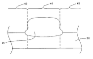
Following nitride surface treatments, active region patterns 42 may be defined on upper surface of silicon nitride layer 30, typically using photoresist. In this regard, any photolithographic or other suitable method for forming a pattern of active device areas may be employed. As shown in FIG. 6, after photoresist is applied silicon nitride film layers 26 and 28 may be removed along with polysilicon buffer layer 24, for example, by anisotropic etching to form field oxide area 40 between active areas 42.
Next, as shown in FIG. 7 field oxide region 44 may be formed on substrate 20 within field oxide area 40. First “bird's beak” areas 46 are present at the surface of substrate 20, but significantly, no second “bird's beak” exists. Field oxide region 44 may be formed using any suitable method known in the art for forming field oxides, including a wet oxidation process, etc. In one embodiment, thickness of field oxide 44 may be from about 1000 Å to about 10,000 Å, alternatively from about 5000 Å to about 9000 Å.
As shown in FIG. 8, following formation of field oxide regions 44, film layers 28 and 26 may be removed in active areas 42 to expose polysilicon buffer layer 24, for example, by chemical etching, HF acid stripping, reactive ion etching, etc. After removal of layers 28 and 26, polysilicon buffer layer 24 and oxide pad layer 22 may be removed in active areas 42, for example, using a dry etching process in one or more steps so as to expose substrate 20 of active region 42, as shown in FIG. 9.
Using embodiments of the disclosed method, nonuniformity of nitridized substrate interfaces may be decreased, resulting in increased process capability. In one exemplary embodiment of the disclosed method, film within wafer thickness nonuniformity (i.e., standard deviation/average wafer thickness) of a nitride treated polysilicon test wafer may be reduced to values as low as about 2% or less, from values of about 7% or more typically seen for surface treatments performed with conventional undoped ammonia plasma treatments.
Table 1 illustrates the difference in film uniformity (i.e., thickness variation) between a standard undoped silicon nitride film formed by conventional ammonia plasma, and a fluorine-doped silicon nitride film formed by a fluorine-doped ammonia plasma, both measured on a 8″ bare silicon test wafer, for one embodiment of the disclosed method.
TABLE 1
Standard NH3 Film vs. C2F6- Doped Film
Standard NH3 Plasma C2F6- Doped Plasma
C2F6 Flow (sccm) 0 30
Thickness (Å) 24 22
Thickness Variation 10 <2
Range (Å)
Wet Oxide Growth (Å) 65 65
Although one exemplary embodiment of the use of a fluorine-doped nitride surface treatment in the creation of a MOS device using a PBLOCOS process has been described above, it will be understood with benefit of the present disclosure that embodiments of the disclosed method may be beneficially employed in any method and/or for the creation of any device in which increased nitride uniformity and/or suppression of “second bird's beak” formation is desired.
EXAMPLES
The following examples are illustrative and should not be construed as limiting the scope of the invention or claims thereof.
Example 1 C2F6 Doped Nitride Surface Treatment
In Example 1, a bare silicon wafer substrate was surface treated using an ammonia PECVD process. FIG. 10 illustrates the reactor set-up utilized, including the spindle puming area 60, wafer position 62, and pumping area limit 64. The process was conducted in a “NOVELLUS CONCEPT II” reactor. The reactor was modified by replacing the mass flow controllers with smaller units acceptable for controlling carbon hexafluorine gas flows of as low as at least 10 sccm. Ammonia and fluorine gases were introduced through separate flow controllers.
In the various tests of this example, CVD treatment gas flow rates ranged from 100 sccm to 200 sccm of C2F6, and from 300 sccm to 400 sccm NH3. The plasma recipe used in this example is given in Table 2.
TABLE 2
C2F6 Doped NH3 Plasma Recipe
(NOVELLUS CONCEPT II Reactor)
Parameter Value
N2 manifold A (sccm) 3000
N2 manifold B (sccm) 3000
NH3 (sccm) 300
C2F6 (sccm) 30
HFRF (watts) 250
LFRF (watts) 350
loPr (torr) 1.9
Pres (torr) 2
hiPr (torr) 2
Temp (° C.) 400
SDT (sec) 12 ± 5
PCT (sec) 120
PreA (sec) 1
PosA (sec) 0.5
Soak (sec) 10
LLwt (sec) 3
flOK (%) 5
Tem % 2
TemT (sec) 1200
depR (A/min) 500
echR (A/min) 2000
PCER (A/min) 2000
pRes (torr) 2.3
SIHE (boolean) 0
WAIT (sec) 5
smFF (boolean) 1
pcLm (A) 20000
SPCT (sec) 60
NH3E (boolean) 1
dfFF (boolean) 0
Thickness and thickness variation was evaluated using a Tencor Instruments “PROMETRIX UV-1250SE.” Results are given in Table 3. Abbreviations used in Table 2 and elsewhere herein are defined as follows:
TABLE 3
Initial Test of C2F6 Doped NH3 Plasma
C2F6 NH3 Wafer Oxide Particles
Flow Flow *SDT Thickness Thickness Growth, Post Plasma
Slot (sccm) (sccm) (sec) (Å) Range (Å) (Å/minute) (number)
 5 100 300 10.4 24.66 1.36 340 1
 6 100 300 10.4 24.49 1.43 340 2
 7 100 300 10.4 24.16 2.18
 8 100 300 10.4 24.42 1.49
 9 100 300 10.4 24.54 1.49
10 100 300 20.4 26.29 1.58
11 100 300 20.4 26.28 1.56
12 200 300 10.4 19.66 3.61
13 200 300 10.4 19.31 2.69
14 100 400 10.4 24.26 1.41
15 100 400 10.4 24.83 1.65
“SDT” = standard deposition time (seconds)
The results of Example 1 indicate that relatively low flow rates of C2F6 result in more desirable oxide growth rates than higher flow rates.
Example 2 C2F6 Doped Nitride Surface Treatment with Lower Flow Rates of C2F6
In Example 2, lower flow rates of C2F6 in the CVD treatment gas were utilized to examine the effect on nitride thickness range and oxide growth. In this example, carbon hexafluorine flow rates ranged from 0 to 100 sccm, while ammonia flow rate was maintained constant at 300 sccm. The experimental apparatus and test procedure of Example 1 were employed for Example 2.
TABLE 4
Lower C2F6 Flow Rates
C2F6 NH3 Thick- Oxide
Flow Flow SDT ness Thickness Growth,
Slot (sccm) (sccm) (sec) (Å) Range (Å) (Å/minute)
1 100 300 10.4 21.25 0.63 925
2 100 300 10.4 20.84 0.95 923
3 0 300 10.4 25.41 9.23 110
4 0 300 10.4 25.51 9.39 113
5 60 300 10.4 22.38 0.49 850
6 60 300 10.4 22.13 0.47 834
Many defects were observed (using the “Tencor 6220”) on the C2F6-doped nitride treated wafers after SiN treatment The defects were actually surface roughness. The particle map matched the 49 pt thickness uniformity map seen after ammonia plasma deposition.
The results of Example 2 indicate that relatively low flows of C2F6 produced desired uniformity benefit while not adversely affecting oxide growth.
Example 3 C2F6 Doped Nitride Surface Treatment with Lower Flow Rates and with D-FEG Setup
In Example 3, the procedure of Example 2 was repeated, this time using a dual frequency e-ground (“D-FEG”) reactor setup. Results of Example 3 are shown in Table 5. In this example, carbon hexafluoride flow rates ranged from 0 sccm to 30 sccm while ammonia flow rate was maintained at 300 sccm.
TABLE 5
Lower C2F6 Flow Rates with D-FEG Setup
Oxide
C2F6 NH3 Thick- Growth,
Flow Flow SDT ness Thickness (Å/minute)
Slot (sccm) (sccm) (sec) (Å) Range (Å) (Avg./Max.)
1  0 300 8.5 25.49 6.65 88/340
2  0 300 8.5 25.64 7.35 83/291
3 30 300 8.5 21.25 1.39 68/117
4 30 300 8.5 20.84 1.48 65/104
The results of this example indicate that maximum oxide growth rate was lower when C2F6 was introduced at the rates indicated.
FIGS. 11 and 12 are contour maps of silicon nitride film thickness for the wafers of slots 1 and 3, respectively. As may be seen by the contour maps, the wafer of slot 3 (surface treated with fluorine-doped ammonia plasma) exhibited a within-wafer thickness variation range of only 1.39 Å over a wafer mean film thickness of 24.19 Å, and had a standard deviation of 0.3329 Å, giving a wafer thickness nonuniformity of 1.376%. This is much more uniform than the 6.65 Å within-wafer thickness range exhibited by the wafer of slot 1 (surface treated with conventional undoped ammonia plasma), which had a mean thickness of 25.49 Å, a standard deviation of 1.9669 Å, and a wafer thickness nonuniformity of 7.717%.
The film uniformity results of Examples 2 and 3 show that a much more uniform interface between the substrate and nitride is achieved when a nitridized interface is created using a fluorine doped ammonia plasma surface treatment. These results also suggest that there is a residence time factor that is not as important when carbon hexafluorine is present in the treatment gas. While not wishing to be bound by theory, such a factor could be a mechanism related to mass transport of reactant ions to the surface, or removal of byproducts. In addition it is possible that highly electronegative fluoride ions modify the ammonia plasma by scavenging hydrogen to form HF, and thus allowing a higher density for reaction with the silicon.
While the invention may be adaptable to various modifications and alternative forms, specific embodiments have been shown by way of example and described herein. However, it should be understood that the invention is not intended to be limited to the particular forms disclosed. Rather, the invention is to cover all modifications, equivalents, and alternatives falling within the spirit and scope of the invention as defined by the appended claims. Moreover, the different aspects of the disclosed compositions and methods may be utilized in various combinations and/or independently. Thus the invention is not limited to only those combinations shown herein, but rather may include other combinations.

Claims (12)

What is claimed is:
1. A method of depositing a substantially uniform fluorine-doped nitridized layer on an upper surface of a substrate in a chemical vapor deposition process, comprising:
exposing a surface of the substrate to a gas mixture comprising a fluorine-containing gas provided at a first steady flow rate and a nitrogen-containing gas provided at a second steady flow rate for a period of time sufficient enough to form a fluorine-doped nitridized layer having an interface with the substrate surface.
2. The method of claim 1, wherein said substrate surface comprises silicon dioxide.
3. The method of claim 1, wherein said substrate surface comprises polysilicon.
4. The method of claim 1, wherein the nitrogen-containing gas is at least one of ammonia, nitrogen, or a mixture thereof; wherein the fluorine-containing gas is at least one of C2F6, C3F8, CF4, or a mixture thereof; and wherein said exposing the substrate surface to the gas mixture occurs in a low pressure plasma enhanced chemical vapor deposition process.
5. The method of claim 1, wherein the nitrogen-containing gas is ammonia; wherein the fluorine-containing gas is carbon hexafluorine; and wherein said exposing the substrate surface to the gas mixture occurs in a low pressure plasma enhanced chemical vapor deposition process.
6. The method of claim 1, further comprising exposing the fluorine-doped nitridized layer to an undoped treatment gas comprising a nitrogen component for a period of time sufficient enough to form an undoped nitridized layer on the fluorine-doped nitridized layer.
7. The method of claim 6, wherein the nitrogen-containing gas of the doped gas mixture is ammonia; wherein the fluorine-containing gas of the doped gas mixture is carbon hexafluorine; wherein the nitrogen component of the undoped treatment gas is ammonia; and wherein said exposing the substrate surface to the doped gas mixture and said exposing the fluorine-doped nitridized layer to the undoped treatment gas each occurs in a respective low pressure plasma enhanced chemical vapor deposition process.
8. The method of claim 5, wherein the fluorine-doped nitridized layer comprises a thickness within the range of about 1 Å to about 40 Å.
9. The method of claim 5, wherein the fluorine-doped nitridized layer comprises a thickness within the range of about 10 Å to about 30 Å.
10. The method of claim 5, wherein the doped gas mixture comprises a gas flow rate ratio of carbonhexafluorine to ammonia that is within the range of about 1:1 to about 1:20.
11. The method of claim 6, wherein the fluorine-doped nitridized layer comprises a thickness of from about 1 Å to about 40 Å; and wherein the undoped nitridized layer comprises a thickness within the range of about 700 Å to about 3000 Å.
12. The method of claim 7, wherein the substrate comprises a semiconductor wafer, and wherein the undoped nitridized layer has a within wafer thickness variation of less than about 2 Å.
US09/862,348 1999-04-26 2001-05-21 Method for forming a nitridized interface on a semiconductor substrate Expired - Fee Related US6495477B2 (en)

Priority Applications (1)

Application Number Priority Date Filing Date Title
US09/862,348 US6495477B2 (en) 1999-04-26 2001-05-21 Method for forming a nitridized interface on a semiconductor substrate

Applications Claiming Priority (2)

Application Number Priority Date Filing Date Title
US29996999A 1999-04-26 1999-04-26
US09/862,348 US6495477B2 (en) 1999-04-26 2001-05-21 Method for forming a nitridized interface on a semiconductor substrate

Related Parent Applications (1)

Application Number Title Priority Date Filing Date
US29996999A Continuation 1999-04-26 1999-04-26

Publications (2)

Publication Number Publication Date
US20010044222A1 US20010044222A1 (en) 2001-11-22
US6495477B2 true US6495477B2 (en) 2002-12-17

Family

ID=23157103

Family Applications (1)

Application Number Title Priority Date Filing Date
US09/862,348 Expired - Fee Related US6495477B2 (en) 1999-04-26 2001-05-21 Method for forming a nitridized interface on a semiconductor substrate

Country Status (3)

Country Link
US (1) US6495477B2 (en)
JP (1) JP3288675B2 (en)
KR (1) KR100381961B1 (en)

Cited By (3)

* Cited by examiner, † Cited by third party
Publication number Priority date Publication date Assignee Title
US10249702B2 (en) 2016-04-19 2019-04-02 International Business Machines Corporation Metal resistors having varying resistivity
US10249703B2 (en) 2016-04-19 2019-04-02 International Business Machines Corporation Metal resistors having nitridized metal surface layers with different nitrogen content
US10276649B2 (en) 2016-04-19 2019-04-30 International Business Machines Corporation Metal resistors having nitridized dielectric surface layers and nitridized metal surface layers

Families Citing this family (3)

* Cited by examiner, † Cited by third party
Publication number Priority date Publication date Assignee Title
US20120276707A1 (en) * 2011-04-28 2012-11-01 Nanya Technology Corporation Method for forming trench isolation
CN102437069B (en) * 2011-11-30 2014-10-15 上海华力微电子有限公司 Method and device for monitoring pretreatment in low-dielectric-constant barrier layer process
KR102651544B1 (en) * 2016-11-21 2024-03-28 삼성전자주식회사 Broadband and multi-purpose optical device and methods of manufacturing and operating the same

Citations (17)

* Cited by examiner, † Cited by third party
Publication number Priority date Publication date Assignee Title
US4764248A (en) 1987-04-13 1988-08-16 Cypress Semiconductor Corporation Rapid thermal nitridized oxide locos process
EP0283306A2 (en) 1987-03-20 1988-09-21 Applied Materials, Inc. Selective thin film etch process
US4897364A (en) 1989-02-27 1990-01-30 Motorola, Inc. Method for locos isolation using a framed oxidation mask and a polysilicon buffer layer
WO1991000615A1 (en) 1989-06-23 1991-01-10 Sgs-Thomson Microelectronics S.A. Method for producing field oxide for a silicon-base integrated circuit
US5264396A (en) 1993-01-14 1993-11-23 Micron Semiconductor, Inc. Method for enhancing nitridation and oxidation growth by introducing pulsed NF3
JPH06350079A (en) 1993-06-07 1994-12-22 Nec Corp Manufacture of semiconductor device
US5382533A (en) 1993-06-18 1995-01-17 Micron Semiconductor, Inc. Method of manufacturing small geometry MOS field-effect transistors having improved barrier layer to hot electron injection
US5397732A (en) 1993-07-22 1995-03-14 Industrial Technology Research Institute PBLOCOS with sandwiched thin silicon nitride layer
US5437765A (en) 1994-04-29 1995-08-01 Texas Instruments Incorporated Semiconductor processing
US5449433A (en) 1994-02-14 1995-09-12 Micron Semiconductor, Inc. Use of a high density plasma source having an electrostatic shield for anisotropic polysilicon etching over topography
JPH09134914A (en) 1995-11-08 1997-05-20 Oki Electric Ind Co Ltd Formation of element isolation region
JPH09321025A (en) 1996-05-30 1997-12-12 Fujitsu Ltd Manufacture of semiconductor device
US5712177A (en) 1994-08-01 1998-01-27 Motorola, Inc. Method for forming a reverse dielectric stack
US5714398A (en) 1996-07-16 1998-02-03 National Science Council Of Republic Of China Self-aligned tungsten strapped source/drain and gate technology for deep submicron CMOS
US5741396A (en) 1994-04-29 1998-04-21 Texas Instruments Incorporated Isotropic nitride stripping
US5804493A (en) 1995-10-11 1998-09-08 Mosel Vitelic, Inc. Method for preventing substrate damage during semiconductor fabrication
US5930655A (en) 1996-11-08 1999-07-27 International Business Machines Corporation Fluorine barrier layer between conductor and insulator for degradation prevention

Family Cites Families (1)

* Cited by examiner, † Cited by third party
Publication number Priority date Publication date Assignee Title
TW405155B (en) * 1997-07-15 2000-09-11 Toshiba Corp Semiconductor device and its manufacture

Patent Citations (17)

* Cited by examiner, † Cited by third party
Publication number Priority date Publication date Assignee Title
EP0283306A2 (en) 1987-03-20 1988-09-21 Applied Materials, Inc. Selective thin film etch process
US4764248A (en) 1987-04-13 1988-08-16 Cypress Semiconductor Corporation Rapid thermal nitridized oxide locos process
US4897364A (en) 1989-02-27 1990-01-30 Motorola, Inc. Method for locos isolation using a framed oxidation mask and a polysilicon buffer layer
WO1991000615A1 (en) 1989-06-23 1991-01-10 Sgs-Thomson Microelectronics S.A. Method for producing field oxide for a silicon-base integrated circuit
US5264396A (en) 1993-01-14 1993-11-23 Micron Semiconductor, Inc. Method for enhancing nitridation and oxidation growth by introducing pulsed NF3
JPH06350079A (en) 1993-06-07 1994-12-22 Nec Corp Manufacture of semiconductor device
US5382533A (en) 1993-06-18 1995-01-17 Micron Semiconductor, Inc. Method of manufacturing small geometry MOS field-effect transistors having improved barrier layer to hot electron injection
US5397732A (en) 1993-07-22 1995-03-14 Industrial Technology Research Institute PBLOCOS with sandwiched thin silicon nitride layer
US5449433A (en) 1994-02-14 1995-09-12 Micron Semiconductor, Inc. Use of a high density plasma source having an electrostatic shield for anisotropic polysilicon etching over topography
US5437765A (en) 1994-04-29 1995-08-01 Texas Instruments Incorporated Semiconductor processing
US5741396A (en) 1994-04-29 1998-04-21 Texas Instruments Incorporated Isotropic nitride stripping
US5712177A (en) 1994-08-01 1998-01-27 Motorola, Inc. Method for forming a reverse dielectric stack
US5804493A (en) 1995-10-11 1998-09-08 Mosel Vitelic, Inc. Method for preventing substrate damage during semiconductor fabrication
JPH09134914A (en) 1995-11-08 1997-05-20 Oki Electric Ind Co Ltd Formation of element isolation region
JPH09321025A (en) 1996-05-30 1997-12-12 Fujitsu Ltd Manufacture of semiconductor device
US5714398A (en) 1996-07-16 1998-02-03 National Science Council Of Republic Of China Self-aligned tungsten strapped source/drain and gate technology for deep submicron CMOS
US5930655A (en) 1996-11-08 1999-07-27 International Business Machines Corporation Fluorine barrier layer between conductor and insulator for degradation prevention

Non-Patent Citations (6)

* Cited by examiner, † Cited by third party
Title
Chang et al., "Improved planarazation techniques applied to a low dielectric constant polyimide used in multilevel metal Ics (invited paper)," Motorola Advanced Technology Center, San Jose, CA, USA, Sep. 12, 1991.
Chiu et al., "A bird's beak free local oxidation technology feasible for VLSI circuits fabrication," IEEE Transactions on Electron Devices, 29(4):536-540, Apr. 1982.
Lee et al., "Ta and TaN adhesion to high-temperature fluorinated polyimides. Surface and interface chemistry," J. of Adhesion Sci. and Tech., 12:773-790, 1998.
Liehr, "In-situ characterization of SiO2 deposition and growth for gate-oxides," SPIE, Rapid Thermal and Integrated Processing, 1595:166-176, 1991.
Morosoff et al., "Plasma polymerization of tetrafluoroethylene. III. capacitive audio frequency (10 kHz) and AC discharge," J. of Applied Polymer Science, 23:3471-3488, 1979.
Wolf, "Silicon Processing for the VLSI Era. vol. 2: Process Integration, Chapter 2, Isolation Technologies for Integrated Circuits," Lattice Press: Sunset Beach, CA, pp. 12-41, 1990.

Cited By (3)

* Cited by examiner, † Cited by third party
Publication number Priority date Publication date Assignee Title
US10249702B2 (en) 2016-04-19 2019-04-02 International Business Machines Corporation Metal resistors having varying resistivity
US10249703B2 (en) 2016-04-19 2019-04-02 International Business Machines Corporation Metal resistors having nitridized metal surface layers with different nitrogen content
US10276649B2 (en) 2016-04-19 2019-04-30 International Business Machines Corporation Metal resistors having nitridized dielectric surface layers and nitridized metal surface layers

Also Published As

Publication number Publication date
KR20010014776A (en) 2001-02-26
JP2001007105A (en) 2001-01-12
US20010044222A1 (en) 2001-11-22
KR100381961B1 (en) 2003-04-26
JP3288675B2 (en) 2002-06-04

Similar Documents

Publication Publication Date Title
US6566727B1 (en) N2O nitrided-oxide trench sidewalls to prevent boron outdiffusion and decrease stress
US6118168A (en) Trench isolation process using nitrogen preconditioning to reduce crystal defects
US7622369B1 (en) Device isolation technology on semiconductor substrate
US6303481B2 (en) Method for forming a gate insulating film for semiconductor devices
US6709951B2 (en) Oxynitride shallow trench isolation and method of formation
US6037018A (en) Shallow trench isolation filled by high density plasma chemical vapor deposition
US6281138B1 (en) System and method for forming a uniform thin gate oxide layer
EP1051744B1 (en) Method of forming a semiconductor device
US7491563B2 (en) Nitridation of STI fill oxide to prevent the loss of STI fill oxide during manufacturing process
US7361572B2 (en) STI liner modification method
US6716685B2 (en) Methods for forming dual gate oxides
JPH09283612A (en) Formation of field oxide film of semiconductor element
WO2008008753A2 (en) A method for fabricating a gate dielectric layer utilized in a gate structure
JPH04354331A (en) Dry etching method
US6444588B1 (en) Anti-reflective coatings and methods regarding same
US6495477B2 (en) Method for forming a nitridized interface on a semiconductor substrate
US6372668B2 (en) Method of forming silicon oxynitride films
US7476916B2 (en) Semiconductor device having a mis-type fet, and methods for manufacturing the same and forming a metal oxide film
US6235654B1 (en) Process for forming PECVD nitride with a very low deposition rate
US6383874B1 (en) In-situ stack for high volume production of isolation regions
US20030096505A1 (en) Manufacturing method of semiconductor device
US6242367B1 (en) Method of forming silicon nitride films
US5863826A (en) CMOS isolation utilizing enhanced oxidation of recessed porous silicon formed by light ion implantation
JPH0831797A (en) Method of selective etching
JPH1050693A (en) Manufacture of semiconductor device

Legal Events

Date Code Title Description
FEPP Fee payment procedure

Free format text: PAYOR NUMBER ASSIGNED (ORIGINAL EVENT CODE: ASPN); ENTITY STATUS OF PATENT OWNER: LARGE ENTITY

FPAY Fee payment

Year of fee payment: 4

FEPP Fee payment procedure

Free format text: PAYER NUMBER DE-ASSIGNED (ORIGINAL EVENT CODE: RMPN); ENTITY STATUS OF PATENT OWNER: LARGE ENTITY

Free format text: PAYOR NUMBER ASSIGNED (ORIGINAL EVENT CODE: ASPN); ENTITY STATUS OF PATENT OWNER: LARGE ENTITY

FPAY Fee payment

Year of fee payment: 8

REMI Maintenance fee reminder mailed
LAPS Lapse for failure to pay maintenance fees
STCH Information on status: patent discontinuation

Free format text: PATENT EXPIRED DUE TO NONPAYMENT OF MAINTENANCE FEES UNDER 37 CFR 1.362

FP Lapsed due to failure to pay maintenance fee

Effective date: 20141217