US6496026B1 - Method of manufacturing and testing an electronic device using a contact device having fingers and a mechanical ground - Google Patents

Method of manufacturing and testing an electronic device using a contact device having fingers and a mechanical ground Download PDF

Info

Publication number
US6496026B1
US6496026B1 US09/512,784 US51278400A US6496026B1 US 6496026 B1 US6496026 B1 US 6496026B1 US 51278400 A US51278400 A US 51278400A US 6496026 B1 US6496026 B1 US 6496026B1
Authority
US
United States
Prior art keywords
fingers
contact
electronic device
substrate
integrated circuit
Prior art date
Legal status (The legal status is an assumption and is not a legal conclusion. Google has not performed a legal analysis and makes no representation as to the accuracy of the status listed.)
Expired - Fee Related
Application number
US09/512,784
Inventor
Tommy Long
Mohamed Sabri
J. Lynn Saunders
Current Assignee (The listed assignees may be inaccurate. Google has not performed a legal analysis and makes no representation or warranty as to the accuracy of the list.)
Microconnect LLC
Original Assignee
Microconnect Inc
Priority date (The priority date is an assumption and is not a legal conclusion. Google has not performed a legal analysis and makes no representation as to the accuracy of the date listed.)
Filing date
Publication date
Application filed by Microconnect Inc filed Critical Microconnect Inc
Priority to US09/512,784 priority Critical patent/US6496026B1/en
Application granted granted Critical
Publication of US6496026B1 publication Critical patent/US6496026B1/en
Assigned to MICROCONNECT LLC reassignment MICROCONNECT LLC ASSIGNMENT OF ASSIGNORS INTEREST (SEE DOCUMENT FOR DETAILS). Assignors: MICROCONNECT, INC.
Anticipated expiration legal-status Critical
Expired - Fee Related legal-status Critical Current

Links

Images

Classifications

    • GPHYSICS
    • G01MEASURING; TESTING
    • G01RMEASURING ELECTRIC VARIABLES; MEASURING MAGNETIC VARIABLES
    • G01R1/00Details of instruments or arrangements of the types included in groups G01R5/00 - G01R13/00 and G01R31/00
    • G01R1/02General constructional details
    • G01R1/06Measuring leads; Measuring probes
    • G01R1/067Measuring probes
    • G01R1/073Multiple probes
    • G01R1/07307Multiple probes with individual probe elements, e.g. needles, cantilever beams or bump contacts, fixed in relation to each other, e.g. bed of nails fixture or probe card
    • G01R1/07342Multiple probes with individual probe elements, e.g. needles, cantilever beams or bump contacts, fixed in relation to each other, e.g. bed of nails fixture or probe card the body of the probe being at an angle other than perpendicular to test object, e.g. probe card

Definitions

  • This invention relates to a contact device for making connection to an electronic circuit device and to methods of fabricating and using such a contact device, such as in the manufacture of semiconductor or other devices.
  • circuits An important aspect of the manufacture of integrated circuit chips is the testing of the circuit embodied in the chip in order to verify that it operates according to specifications. Although the circuit could be tested after the chip has been packaged, the expense involved in dicing the wafer and packaging the individual chips makes it preferable to test the circuit as early as possible in the fabrication process, so that unnecessary efforts will not be expended on faulty devices. It is therefore desirable that the circuits be tested either immediately after wafer fabrication is completed, and before separation into dice, or after dicing, but before packaging. In either case, it is necessary to make electrical connection to the circuits' external connection points (usually bonding pads) in a non-destructive way, so as not to interfere with subsequent packaging and connection operations.
  • external connection points usually bonding pads
  • U.S. Pat. No. 5,221,895 discloses a probe for testing integrated circuits.
  • the probe includes a stiff metal substrate made of beryllium copper alloy, for example.
  • the substrate is generally triangular in form and has two edges that converge from a support area toward a generally rectangular tip area.
  • the conductor runs and the metal substrate form microstrip transmission lines.
  • the conductor runs extend parallel to one another over the tip area and fan out toward the support area.
  • a contact bump is deposited on the end of each conductor run that is on the tip area.
  • the tip area of the substrate is slit between each two adjacent conductor runs whereby the tip area is divided into multiple separately flexible fingers that project in cantilever fashion from the major portion of the substrate.
  • the probe shown in U.S. Pat. No. 5,221,895 is designed to be used in a test station.
  • a test station may include four probes having the configuration shown in U.S. Pat. No. 5,221,895, the probes being arranged in an approximately horizontal orientation with their contact bumps facing downwards, with the four rows of contact bumps along four edges of a rectangle.
  • the DUT is generally rectangular and has connection pads along the edges of one face.
  • the DUT is placed in a vacuum chuck with its connection pads upwards.
  • the vacuum chuck drives the DUT upward into contact with the probe, and overdrives the DUT by a predetermined distance from first contact.
  • such a test station is designed to produce a nominal contact force of 10 grams at each connection pad. Therefore, the amount of the overdrive is calculated to be such that if contact is made at all connection pads simultaneously, so that each contact bump is deflected by the same amount, the total contact force will be 10 grams force multiplied by the number of connection pads.
  • the material of the probe substrate is a beryllium copper alloy and each flexible finger has a length of about 0.75 mm, a width of about 62 microns and a height of about 250 microns, and the probe is supported so that the mechanical ground is at the root of the fingers, the contact force produced at the tip of the finger is about 7.7 grams for each micrometer of deflection of the tip of the finger. Therefore, if the contact bumps at the tips of the fingers are coplanar and the connection pads of the DUT are coplanar, and the plane of the contact bumps is parallel to the plane of the connection pads, an overdrive of about 1.3 microns from first contact will result in the desired contact force of 10 grams at each connection pad.
  • connection pads should be 1.3 microns farther from the plane of the contact bumps than the other connection pads, when the DUT is displaced by 1.3 microns from first contact, there will be no contact force between this connection pad and its contact bump, and all the contact force that is generated will be consumed by the other contacts. If one assumes that the contact force at a connection pad must be at least 50 percent of the nominal contact force in order for there to be a reliable connection, then the maximum variance from the nominal height that this design will accommodate is ⁇ 0.7 microns. However, the height variations of contact bumps and connection pads produced by the standard processes currently employed in the semiconductor industry typically exceed 5 microns.
  • connection pads of the DUT are not coplanar, nor are the connection bumps on the probe. Assuming that the nominal plane of the connection pads (the plane for which the sum of the squares of the distances of the pads from the plane is a minimum) is parallel with the nominal plane of the contact bumps, the variation in distance between the connection pad and the corresponding contact bump is up to 5 microns if both the DUT and the probe are of good quality.
  • connection points on an integrated circuit chip are at a pitch of at least 150 microns, but it is expected that it will be feasible for the pitch to be reduced to about 100 microns within a few years.
  • connection pads are at a spacing of 75 microns, this implies that the width of the fingers must be less than about 50 microns, and in order to keep the stress below the yield point, the height of the fingers must be at least 400 microns.
  • the necessary height of the fingers can be reduced by employing a metal of which the yield point is higher than that of beryllium copper.
  • a metal of which the yield point is higher than that of beryllium copper For example, if the substrate is made of stainless steel, having an elastic modulus of 207 ⁇ 10 9 N/m 2 , the maximum height of the fingers can be reduced to about 350 microns.
  • the resistivity of stainless steel is substantially higher than that of beryllium copper, and this limits the frequency of the signals that can be propagated by the microstrip transmission lines without unacceptable degradation.
  • prior techniques found limited application due to difficulties in achieving adequate deflection with the necessary force to achieve reliable connection, while withstanding the generated stresses.
  • microstrip transmission line has adequate characteristics for signals up to a frequency of 5 GHz, and it has been discovered that the so-called stripline configuration is desirable for higher frequencies.
  • a method of making a multilayer composite structure for use in manufacture of a contact device for establishing electrical connection to a circuit device comprising providing a substrate of a metal having a resistivity substantially greater than about 10 micro-ohm cm, adhering a first layer of metal having a resistivity less than about 3 micro-ohm cm to a main face of the substrate, the first layer having a main face that is remote from the substrate, adhering a second layer of dielectric material to the main face of the first layer, the second layer having a main face that is remote from the substrate, and adhering a third layer of metal to the main face of the second layer, the metal of the third layer having a resistivity less than abut 3 micro-ohm cm.
  • a method of making a contact device for use in establishing electrical connection to a circuit device comprising providing a substrate of a metal having a resistivity substantially greater than about 10 micro-ohm cm, the substrate having a major portion and a tip portion projecting therefrom along an axis, adhering a first layer of metal having a resistivity less than about 3 micro-ohm cm to a main face of the substrate, the first layer having a main face that is remote from the substrate, adhering a second layer of dielectric material to the main face of the first layer, the second layer having a main face that is remote from the substrate, adhering a third layer of metal to the main face of the second layer, the metal of the third layer having a resistivity less than about 3 micro-ohm cm, selectively removing metal of the third layer to form discrete conductor runs extending over the tip portion parallel to said axis, while leaving portions of the second layer exposed between the conductor runs, where
  • a probe apparatus for use in testing an integrated circuit embodied in an integrated circuit chip, said probe apparatus comprising a support member having a generally planar datum surface, a generally planar elastic probe member having a proximal end and a distal end, at least one attachment member attaching the probe member at its proximal end to the support member with the probe member in contact with the datum surface, at least one adjustment member effective between the support member and a location on the probe member that is between the proximal and distal ends thereof for urging the distal end of the probe member away from the support member, whereby the probe member undergoes elastic deflection.
  • a probe apparatus for use in testing an integrated circuit embodied in an integrated circuit chip, said probe apparatus comprising a support member having a bearing surface, a probe member having a proximal end and a distal end and comprising a stiff substrate having first and second opposite main faces and conductor runs extending over the first main face of the substrate from the distal end of the substrate to the proximal end thereof, the conductor runs of the probe member being distributed over a connection region of the first main face of the substrate in a first predetermined pattern, at least one attachment member attaching the probe member to the support member with the second main face of the probe member confronting the bearing surface of the support member, a circuit board comprising a substrate having a main face and conductor runs distributed over a connection region of said main face of the circuit board in a second predetermined pattern, a flexible circuit comprising a flexible substrate having a main face and first and second connection regions, and conductor runs extending between the first and second connection regions of the flexible
  • a method of making a multilayer composite structure for use in manufacture of a contact device for establishing electrical connection to a circuit device comprising providing a substrate, adhering a first layer of dielectric material to a main face of the substrate, the first layer having a main face that is remote from the substrate, and adhering a second layer of metal to the main face of the first layer, the metal of the second layer having a resistivity less than about 3 micro-ohm cm.
  • a method of making a contact device for use in establishing electrical connection to a circuit device comprising providing a substrate having a major portion and a tip portion projecting therefrom along an axis, adhering a first layer of dielectric material to the main face of the substrate, the first layer having a main face that is remote from the substrate, adhering a second layer of metal to the main face of the first layer, the metal of the second layer having a resistivity less than about 3 micro-ohm cm, selectively removing metal of the second layer to form discrete conductor runs extending over the tip portion parallel to said axis, while leaving portions of the first layer exposed between the conductor runs, whereby a multilayer composite structure is formed, and slitting the tip portion of the composite structure parallel to said axis, whereby fingers are formed that project from the major portion of the composite structure in cantilever fashion and each of which supports at least one conductor run.
  • a contact device having a plurality of nominally coplanar first contact elements for making electrical contact with corresponding nominally coplanar second contact elements of an electronic device by positioning the contact device and the electronic device so that the plane of the first contact elements is substantially parallel to the plane of the second contact elements and effecting relative displacement of the devices in a direction substantially perpendicular to the plane of the first contact elements and the plane of the second contact elements to generate a contact force of at least f at each pair of corresponding first and second contact elements, wherein it is necessary to effect relative displacement of the devices by a distance d in said direction from first touchdown to last touchdown, said contact device comprising a stiff substrate having a major portion with fingers projecting therefrom in cantilever fashion, each finger having a proximal end at which it is connected to the major portion of the substrate and an opposite distal end and there being at least one, and no more than two, contact elements on the distal end of each finger, a support member to which the substrate is attached in
  • a method for testing/manufacturing devices such as integrated circuits or displays (such as LCD panels), which may include the steps of carrying out a manufacturing process for the DUT, such as a planar-type integrated circuit manufacturing process, positioning the DUT on a positioning device, such as a vacuum chuck (the DUT may be in wafer or die form, in the case of integrated circuits, etc.), effecting alignment of a contact device in accordance with the present invention with the DUT to the extent required for proper placement, effecting relative movement of the DUT with respect to the contact device to establish initial contact thereto (as determined electrically or by a mechanical means), over-driving the relative movement to establish reliable electrical connection, wherein stresses are desirably shared between the extended fingers of the contact device and the substrate of the contact device, applying test signals to the DUT and determining whether the DUT is defective or otherwise within or outside acceptable specifications, recording whether the pass/fail condition of the DUT (which may include mechanical notation, such
  • devices with connection points of fine pitch may be reliably tested and manufactured.
  • FIGS. 1-5 illustrate various steps during fabrication of a contact device embodying the present invention, FIGS. 1 and 4 being plan views and FIGS. 2, 3 and 5 being sectional views;
  • FIG. 6 is a partial perspective view of a contact device embodying the invention.
  • FIG. 6A is a sectional view on the line VIA—VIA of FIG. 6;
  • FIG. 7 is a general view, partly in section, of a semiconductor tester
  • FIG. 8 is a plan view of a circuit board and mounting plate that form part of the test head of the tester shown in FIG. 7;
  • FIG. 9 is an enlarged perspective view of the mounting plate and also illustrates back-up blocks that are attached to the mounting plate;
  • FIGS. 9A, 9 B, and 9 C are sectional view illustrating the manner in which the back-up blocks are attached to the mounting plate
  • FIG. 10 is an enlarged view of a flexible circuit that is used to connect the circuit board to the contact device
  • FIGS. 11A and 11B are sectional views illustrating the manner in which the contact device and the flexible circuit are positioned relative to the mounting block.
  • FIGS. 12A and 12B are sectional views illustrating the manner in which the mounting plate and the flexible circuit are positioned relative to the circuit board.
  • FIG. 1 illustrates a substrate 4 of elastic metal having an upper main face 6 and a lower main face.
  • the substrate is stainless steel and is about 125 microns thick.
  • the substrate is generally triangular in form, having two edges 8 that converge from a support area 10 toward a generally rectangular tip area 12 .
  • the substrate is substantially mirror-image symmetrical about a central axis 18 .
  • a thin film 14 of gold is deposited on the upper main face 6 of the substrate 4 by evaporation or sputtering.
  • the gold film may be augmented by plating if desired.
  • An insulating material such as polyimide is spun or sprayed onto the upper main face of the film 14 in the liquid phase and is then cured to form a layer 16 about 25 microns thick.
  • a layer 20 of gold is deposited over the upper main face 22 of the layer 16 by evaporation or sputtering.
  • the layer 20 is patterned using conventional photolithographic techniques to form strips 26 that extend parallel to the central axis 18 over the tip area 12 of the probe and fan out from the tip area over the triangular part of the substrate 4 toward the support area 10 but which may be connected together at the support area.
  • Each strip has a proximal end and a distal end relative to the support area 10 .
  • Additional metal is then deposited over the strips by plating.
  • a layer 30 of photomask material (FIG. 5) is deposited over the upper surface of the structure shown in FIGS.
  • a cover layer 40 of polyimide is formed over the conductor runs 26 , over a region of the substrate that is to the rear, i.e. toward the support area 10 , of the rectangular tip area 12 and a layer 44 of gold is deposited over the layer 40 by evaporation or sputtering.
  • the layer 44 may be augmented by plating.
  • the tip area of the multilayer structure is then slit, whereby the tip area is divided into multiple separately flexible fingers 48 that project in cantilever fashion from the major portion of the structure.
  • a given finger of the substrate may carry the distal end portion of a single conductor run, or it may carry the distal end portions of two adjacent conductor runs.
  • the slitting of the tip area may be performed by ablation using a ultraviolet laser.
  • the poor thermal conductivity of stainless steel is a favorable factor with regard to the laser ablation process.
  • the width of the kerf that is removed is about 17 microns, so that the width of a finger is either about 108 microns or about 233 microns.
  • the length of each finger is about 1 mm.
  • the structure shown in FIG. 6 may be used as a contact device for making electrical connection to contact pads of an electrical circuit device, such as an integrated circuit chip or a flat panel display device.
  • the nickel bumps 34 serve as probe elements for contacting the connection pads of the circuit device. When the contact device is in use, each nickel bump contacts a single connection pad of the circuit device.
  • a bump 34 a that is to contact a ground pad of the circuit device may be connected to the substrate by means of vias 46 formed in holes in the layer 16 before depositing the layer 20 . Multiple vias 46 may be provided along the length of the conductor run 26 that ends at the bump 34 a in order to ensure that the contact bump 34 a is firmly grounded.
  • the configuration of the conductor runs and their spacing results in there being a stripline transmission line environment to the rear of the forward boundary of the layer 44 , whereas there is a microstrip transmission line environment forward of the layer 44 .
  • the slitting of the tip area results in degradation of the microstrip transmission line environment.
  • the microstrip transmission line environment extends to a point that is about 2 mm from the contact bumps.
  • the degradation is not so severe as to distort signals at frequencies below about 10 GHz to an unacceptable degree.
  • the structure shown in FIG. 6 may be used for probing a circuit device in a semiconductor tester, as will be described with reference to FIGS. 7-11.
  • the tester comprises a prober 102 having a frame 102 a that serves as a mechanical ground.
  • a device positioner 104 having a vacuum chuck 106 is mounted within or as part of the prober 102 .
  • the prober includes stepping motors (not shown) that act on the device positioner for translating the vacuum chuck relative to the frame 102 a in two perpendicular horizontal directions (X and Y) and vertically (Z), and for rotating the vacuum chuck about a vertical axis.
  • the vacuum chuck holds a device under test, or DUT, 108 .
  • the DUT 108 illustrates the DUT 108 as a die that has previously been separated from other dice of the wafer in which it was fabricated, but it will be appreciated that, with appropriate modifications, the apparatus could be used for testing a semiconductor device at the wafer stage. As shown in FIG. 7, the DUT 108 has contact pads 112 .
  • the tester also comprises a test head 116 that can be docked to the prober so that it is in a reliably reproducible position relative to the prober frame 102 a .
  • the test head 116 includes an essentially rigid circuit board 122 (FIG. 8) that comprises an insulating substrate and conductor runs 126 exposed at the lower main face of the substrate. Vias (not shown) extend through the substrate and terminate at contact pads 128 that are exposed at the upper main face of the substrate.
  • the circuit board 122 is removably held in the test head by screws that pass through holes 130 in the circuit board.
  • the circuit board 122 When the test head 116 is docked in the prober 102 and the circuit board 122 is installed in the test head, the circuit board 122 is disposed horizontally and the contact pads 128 engage pogo pins 132 , shown schematically in FIG. 7, by which the contact pads of the circuit board are connected to stimulus and response instruments (not shown), for purposes of conducting appropriate tests on the DUT.
  • a mounting plate 136 is secured to the circuit board 122 .
  • the mounting plate is positioned relative to the circuit board by guide pins 134 that project downward from the mounting plate and enter corresponding holes in the circuit board. The manner in which the mounting plate is attached to the circuit board will be described below.
  • the mounting plate has a generally cylindrical exterior surface of which the central axis 138 is considered to be the axis of the plate.
  • the plate 136 is disposed with its axis 138 vertical and defines a cross-shaped through opening (FIG. 9) that is mirror image symmetrical about X-Z and Y-Z planes that intersect at the axis 138 .
  • the plate 136 is formed with a notch 140 that extends only part way through the plate and is bounded in the vertically downward direction by a horizontal surface 142 .
  • a backup block 146 having the general shape, when viewed in plan, of a trapezoid seated on a rectangular base is positioned with its rectangular base in one of the notches 140 .
  • Similar backup blocks 148 are mounted in the other notches. The following description of the backup block 146 and associated components applies equally to the backup blocks 148 .
  • the rectangular base of the backup block 146 has a planar mounting surface 150 (FIG. 7) that can be seated against the horizontal surface 142 at the bottom of the notch 140 .
  • the backup block is formed with a hole 152 extruding through its rectangular base, and the mounting plate is formed with a blind hole 156 that is parallel to the axis of the mounting plate and enters the plate 136 at the horizontal surface 142 .
  • a guide pin 160 is inserted through the hole 152 in the backup block and into the blind hole 156 in the mounting plate, and in this manner the backup block is positioned with a moderate degree of precision relative to the mounting plate.
  • the backup block 146 is then attached to the mounting plate 136 by a vertical locking screw 164 (FIG. 8, FIG. 9A) that passes through a clearance hole 168 in the backup block 146 and enters a threaded bore 172 in the mounting plate 136 and a horizontal locking screw 176 (FIG. 7) that passes through a clearance hole 180 in the mounting plate and enters a threaded bore 184 in the backup block.
  • the backup block 146 is thereby attached to the mounting plate, and the guide pin 160 is then removed.
  • the clearance holes 168 and 180 allow a small degree of horizontal and vertical movement of the backup block relative to the mounting plate.
  • Two horizontal screws 186 which are horizontally spaced and disposed one on each side of the screw 176 , are inserted through threaded holes in the peripheral wall of the plate 136 and enter blind clearance holes in the backup block.
  • two vertical screws 190 which are horizontally spaced and disposed one on each side of the screw 164 , are inserted through threaded holes in the backup block 146 and engage the surface 142 of the mounting plate 136 .
  • the screws 176 and 186 can be used to adjust the horizontal position of the backup block relative to the mounting plate 136 .
  • the backup block can be advanced or retracted linearly and/or rotated about a vertical axis.
  • the backup block can be raised or lowered relative to the mounting plate and/or tilted about a horizontal axis. When the backup block is in the desired position and orientation, the locking screws are tightened.
  • the apparatus shown in FIGS. 7-10 also comprises a contact device 194 associated with the backup block 146 .
  • the contact device 194 is generally triangular and has two edges that converge from a support area toward a generally rectangular tip area.
  • the tip area of the contact device is divided into multiple fingers that extend parallel to an axis of symmetry of the contact device.
  • the contact device includes conductor runs that extend from the support area to the tip area, and one run extends along each finger in the tip area. At its support area, the conductor runs of the contact device are exposed on the underside of the contact device.
  • the contact device may be fabricated by the method that is described above with reference to FIGS. 1-6.
  • the trapezoidal portion of the backup block 146 extends downward toward the central axis 138 .
  • the contact device 194 is disposed below the inclined lower surface of the backup block 146 and is positioned relative to the backup block by guide pins 202 (e.g., FIGS. 11A and 11B) that project from the backup block and pass through alignment holes 204 in the contact device. The manner in which the contact device is attached to the backup block will be described below.
  • the apparatus also comprises a flexible circuit 208 having an inner edge region 208 A and an outer edge region 208 B (e.g., FIG. 10 ).
  • the flexible circuit comprises a substrate of polyimide or similar insulating material, a ground plane (not shown) on the lower side of the substrate, and multiple discrete conductor runs 210 on the upper side of the substrate.
  • the spacing of the conductor runs 210 corresponds to the spacing of the conductor runs across the support area of the contact device 194
  • the spacing of the conductor runs 210 corresponds to the spacing of the conductor runs 126 along the inner edge of the printed circuit board 122 .
  • the flexible circuit is formed with inner and outer pairs of alignment holes 214 A and 214 B.
  • the inner pair of alignment holes 214 A are threaded by the guide pins 202 , whereby the inner edge region 208 A is positioned relative to the contact device 194 .
  • the outer pair of alignment holes 214 B are threaded by the guide pins 134 , whereby the outer edge region 208 B of the flexible circuit is positioned relative to the printed circuit board.
  • the flexible circuit is also formed with two sets of mounting holes 218 A and 218 B.
  • the support area of the contact device 194 , the inner edge region 208 A of the flexible circuit, and a first length 22 A of Shinetsu strip are clamped between the backup block and a clamping plate 226 A by means of screws 230 A.
  • the outer edge region 208 B of the flexible circuit 208 , the inner region of the printed circuit board 122 , and a second length 222 B of Shinetsu strip are clamped between the mounting plate 136 and a second clamping plate 226 B by means of screws 230 B.
  • the positions of the alignment holes 214 A and 214 B relative to the conductor runs of the flexible circuit are such that the conductor runs 210 at the inner edge region 208 A of the flexible circuit are in registration with the conductor runs 26 in the support area of the contact device, and the conductor runs 210 in the outer edge region 208 B of the flexible circuit are in registration with the conductor runs 126 along the inner edge of the printed circuit board.
  • the Shinetsu strip is characterized by anisotropic electrical conductivity when compressed perpendicular to its length: its conductivity is very good in directions perpendicular to its own plate and is very bad in directions parallel to its own plane and to its length.
  • the Shinetsu strip 222 A connects the conductor runs 26 of the probe member 194 to respective conductor runs 210 of the flexible circuit 208
  • the Shinetsu strip 222 B connects the conductor runs 210 of the flexible circuit 208 to respective conductor runs 126 of the printed circuit board 122 .
  • the tip area of the contact device 194 is divided into fingers, each of which has a contact run that terminates in a contact bump. Since the tip area is spaced from the support area, at which the contact device is clamped to the backup block, the tip area can be deflected away from the plane of the underside of the backup block.
  • Vertical adjustment screws 234 are fitted in respective threaded holes in the backup block 146 . By appropriate adjustment of the screws 234 , the contact device can be preloaded to a condition in which the contact device 194 is deflected downwards relative to the backup block 146 , and by further adjustment of the screws 234 the tip area can be forced downward, or permitted to rise, or tilted about the axis 18 .
  • the “mechanical ground” therefore extends to a location of the contact device that is beyond the support area but does not extend as far as the lip area. As described more fully below, proper positioning of mechanical ground can enable stress sharing between the fingers of the contact device and the contact device substrate, thereby enabling the contact device to withstand the stresses that result from applying force sufficient to ensure reliable contact between the DUT and the contact device, given the irregularities that can be expected in actual devices/conditions.
  • the tip portions of the four contact devices extend along four edges of a square and are positioned for making electrically conductive contact to the contact pads of the device under test.
  • the DUT can be positioned for contacting the contact bumps when the DUT is raised by the positioning device.
  • the contact pads of the DUT engage the contact bumps of the contact device.
  • the DUT is raised an initial 10-15 microns, which is sufficient to absorb any expected error in coplanarity of the contact bumps and contact pads and achieve last touchdown (each contact bump is in contact with its respective contact pad).
  • the DUT is then raised by a further 75 microns.
  • the spring rate of the fingers and the spring rate of the base region of the substrate, between the fingers and the support area, are such that the contact force exerted at each contact pad is at least 10 grams.
  • the initial deflection of 10-15 microns is sufficient to provide a contact force of about 2 grams at a single finger, whereas the further deflection of 75 microns provides a contact force of N*10 grams, where N is the number of fingers, or 10 grams per finger.
  • the elastic nature of the metal of the substrate ensures that when the DUT is brought into contact with the contact bumps, and is slightly over driven, deflection of the fingers provides a desirable scrubbing action and also supplies sufficient contact force for providing a reliable pressure contact between the contact bump and the connection pad of the DUT.
  • the film 14 of gold serves as the ground plane, and the substrate 4 , although conductive, does not contribute to the electrical performance of the device.
  • the present invention achieves desirous stress load sharing between the fingers and the substrate. It has been determined that with available materials, to be of practical size and provide suitable compliance/deflection of the fingers (such as to accommodate deviations from coplanarity, etc.), stress loads induced in the fingers and the substrate should be balanced (i.e., maintained in an acceptable relative range, below the stress limit of the material). Proper positioning of a mechanical ground between the ends of the fingers and the back extremity of the support area can enable controlled balancing of the relative stress loads, while also ensuring an adequate deflection of the fingers to achieve adequate compliance.
  • the relative stress loads of the fingers and substrate are maintained/balanced in a ranges of about 0.7 to 1.3, 0.8 to 1.2 or 0.9 to 1.1. Other ranges may be utilized, provided that a desirable balance is maintained, while of meeting the conditions of adequate deflection/compliance in the fingers, while staying within the stress limits of the constant materials.
  • the length of the fingers controlled by the length of the slit and overall physical geometry, etc., can be chosen to give the desired finger deflection/compliance, such as a desired deflection of greater than about 10 microns, 12, microns or 15 microns, in the case of, for example, 60-80 or 75 microns, etc., of overdrive, while maintaining stress balancing as described above, can produce a probe element that produces reliable connection with the DUT while surviving the resulting stress loads, etc.
  • the present invention may be desirably applied to the testing and manufacture of devices such as integrated circuits or displays (such as LCD panels).
  • a manufacturing process for the DUT 108 is conducted, such as a planar-type integrated circuit manufacturing process.
  • an appropriate LCD or other manufacturing process is conducted.
  • the DUT 108 on a positioning device, such as a vacuum chuck 106 of prober 102 (the DUT may be in wafer or die form, in the case of integrated circuits, etc.).
  • the DUT 108 is aligned with contact device 194 to the extent required for proper placement. Thereafter, relative movement is effected of the DUT 108 with respect to the contact device 194 to establish initial contact therebetween (as determined electrically or by a known mechanical means).
  • test signals are applied to the DUT 108 and it is electrically determined whether the DUT is defective or otherwise within or outside acceptable specifications.
  • the pass/fail condition of the DUT may be recorded (which may include mechanical notation, such as inking the DUT if defective, etc., or by data recording). Still thereafter, the DUT 108 may be removed from the positioning device. If the device is acceptable, known packaging and assembling of the DUT may be performed.
  • devices with connection points of fine pitch may be reliably tested and manufactured.

Abstract

A contact device having a plurality of nominally coplanar first contact elements makes electrical contact with corresponding nominally coplanar second contact elements of an electronic device when the contact device and the electronic device are positioned so that the plane of the first contact elements is substantially parallel to the plane of the second contact elements and relative displacement of the devices is effected in a direction substantially perpendicular to the plane of the first contact elements and the plane of the second contact elements. The contact device comprises a stiff substrate having a major portion with fingers projecting therefrom in cantilever fashion, each finger having a proximal end at which it is connected to the major portion of the substrate and an opposite distal end and there being one or two contact elements on the distal end of each finger. It is necessary to effect relative displacement of the devices by a distance d from first touchdown to achieve last touchdown. The substrate is dimensioned such that relative displacement of the devices by a distance d from first touchdown generates a reaction force at each contact element of about 0.1*f±0.1*f, and further relative displacement by a distance of about 75 microns or 5*d beyond last touchdown generates a reaction force at each contact element of about 0.9±0.1*f.

Description

This is a Divisional application of U.S. patent application Ser. No. 08/765,661, filed Mar. 4, 1997, now U.S. Pat. No. 6,046,599 which was filed based on PCT/US96/07359, filed May 20, 1996, which claimed priority based on application Ser. No. 08/446,020, filed May 19, 1995, now U.S. Pat. No. 5,621,333.
BACKGROUND OF THE INVENTION
This invention relates to a contact device for making connection to an electronic circuit device and to methods of fabricating and using such a contact device, such as in the manufacture of semiconductor or other devices.
An important aspect of the manufacture of integrated circuit chips is the testing of the circuit embodied in the chip in order to verify that it operates according to specifications. Although the circuit could be tested after the chip has been packaged, the expense involved in dicing the wafer and packaging the individual chips makes it preferable to test the circuit as early as possible in the fabrication process, so that unnecessary efforts will not be expended on faulty devices. It is therefore desirable that the circuits be tested either immediately after wafer fabrication is completed, and before separation into dice, or after dicing, but before packaging. In either case, it is necessary to make electrical connection to the circuits' external connection points (usually bonding pads) in a non-destructive way, so as not to interfere with subsequent packaging and connection operations.
U.S. Pat. No. 5,221,895 discloses a probe for testing integrated circuits. The probe includes a stiff metal substrate made of beryllium copper alloy, for example. The substrate is generally triangular in form and has two edges that converge from a support area toward a generally rectangular tip area. There is a layer of polyimide over one main face of the substrate, and gold conductor runs are formed over the layer of polyimide. The conductor runs and the metal substrate form microstrip transmission lines. The conductor runs extend parallel to one another over the tip area and fan out toward the support area. A contact bump is deposited on the end of each conductor run that is on the tip area. The tip area of the substrate is slit between each two adjacent conductor runs whereby the tip area is divided into multiple separately flexible fingers that project in cantilever fashion from the major portion of the substrate.
The probe shown in U.S. Pat. No. 5,221,895, is designed to be used in a test station. Such a test station may include four probes having the configuration shown in U.S. Pat. No. 5,221,895, the probes being arranged in an approximately horizontal orientation with their contact bumps facing downwards, with the four rows of contact bumps along four edges of a rectangle. The DUT is generally rectangular and has connection pads along the edges of one face. The DUT is placed in a vacuum chuck with its connection pads upwards. The vacuum chuck drives the DUT upward into contact with the probe, and overdrives the DUT by a predetermined distance from first contact. According to current industry standards, such a test station is designed to produce a nominal contact force of 10 grams at each connection pad. Therefore, the amount of the overdrive is calculated to be such that if contact is made at all connection pads simultaneously, so that each contact bump is deflected by the same amount, the total contact force will be 10 grams force multiplied by the number of connection pads.
If the material of the probe substrate is a beryllium copper alloy and each flexible finger has a length of about 0.75 mm, a width of about 62 microns and a height of about 250 microns, and the probe is supported so that the mechanical ground is at the root of the fingers, the contact force produced at the tip of the finger is about 7.7 grams for each micrometer of deflection of the tip of the finger. Therefore, if the contact bumps at the tips of the fingers are coplanar and the connection pads of the DUT are coplanar, and the plane of the contact bumps is parallel to the plane of the connection pads, an overdrive of about 1.3 microns from first contact will result in the desired contact force of 10 grams at each connection pad. However, if one of the connection pads should be 1.3 microns farther from the plane of the contact bumps than the other connection pads, when the DUT is displaced by 1.3 microns from first contact, there will be no contact force between this connection pad and its contact bump, and all the contact force that is generated will be consumed by the other contacts. If one assumes that the contact force at a connection pad must be at least 50 percent of the nominal contact force in order for there to be a reliable connection, then the maximum variance from the nominal height that this design will accommodate is ±0.7 microns. However, the height variations of contact bumps and connection pads produced by the standard processes currently employed in the semiconductor industry typically exceed 5 microns.
Furthermore, even if the contact bumps are coplanar and the connection pads are coplanar, tolerances in the probing apparatus make it impossible to ensure that the plane of the connection pads is parallel to the plane of the contact bumps, and, in order to accommodate these tolerances, it is necessary to displace the DUT by 75 microns in order to ensure contact at all connection pads. If the dimensions of the finger were changed to accommodate a displacement of 70-80 microns (75 microns±5 microns), the probe would become much less robust. If the probe were supported at a location further back from the root of the fingers, such that most of the deflection would be carried by the substrate rather than the fingers, the ability of the fingers to conform would be limited to 0.13 microns/gram deflection produced at the fingers themselves.
The connection pads of the DUT are not coplanar, nor are the connection bumps on the probe. Assuming that the nominal plane of the connection pads (the plane for which the sum of the squares of the distances of the pads from the plane is a minimum) is parallel with the nominal plane of the contact bumps, the variation in distance between the connection pad and the corresponding contact bump is up to 5 microns if both the DUT and the probe are of good quality.
At present, the connection points on an integrated circuit chip are at a pitch of at least 150 microns, but it is expected that it will be feasible for the pitch to be reduced to about 100 microns within a few years.
As the need arises to make connection at ever finer pitches, the stress in a probe of the kind shown in U.S. Pat. No. 5,221,895 increases. If the connection pads are at a spacing of 75 microns, this implies that the width of the fingers must be less than about 50 microns, and in order to keep the stress below the yield point, the height of the fingers must be at least 400 microns.
The necessary height of the fingers can be reduced by employing a metal of which the yield point is higher than that of beryllium copper. For example, if the substrate is made of stainless steel, having an elastic modulus of 207×109 N/m2, the maximum height of the fingers can be reduced to about 350 microns. However, it follows that the deflection is reduced below that necessary to comply with typical height variations found in the industry. Additionally, the resistivity of stainless steel is substantially higher than that of beryllium copper, and this limits the frequency of the signals that can be propagated by the microstrip transmission lines without unacceptable degradation. In general, prior techniques found limited application due to difficulties in achieving adequate deflection with the necessary force to achieve reliable connection, while withstanding the generated stresses.
In addition, although the microstrip transmission line has adequate characteristics for signals up to a frequency of 5 GHz, and it has been discovered that the so-called stripline configuration is desirable for higher frequencies.
SUMMARY OF THE INVENTION
In accordance with a first aspect of the present invention there is provided a method of making a multilayer composite structure for use in manufacture of a contact device for establishing electrical connection to a circuit device, said method comprising providing a substrate of a metal having a resistivity substantially greater than about 10 micro-ohm cm, adhering a first layer of metal having a resistivity less than about 3 micro-ohm cm to a main face of the substrate, the first layer having a main face that is remote from the substrate, adhering a second layer of dielectric material to the main face of the first layer, the second layer having a main face that is remote from the substrate, and adhering a third layer of metal to the main face of the second layer, the metal of the third layer having a resistivity less than abut 3 micro-ohm cm.
In accordance with a second aspect of the present invention there is provided a method of making a contact device for use in establishing electrical connection to a circuit device, said method comprising providing a substrate of a metal having a resistivity substantially greater than about 10 micro-ohm cm, the substrate having a major portion and a tip portion projecting therefrom along an axis, adhering a first layer of metal having a resistivity less than about 3 micro-ohm cm to a main face of the substrate, the first layer having a main face that is remote from the substrate, adhering a second layer of dielectric material to the main face of the first layer, the second layer having a main face that is remote from the substrate, adhering a third layer of metal to the main face of the second layer, the metal of the third layer having a resistivity less than about 3 micro-ohm cm, selectively removing metal of the third layer to form discrete conductor runs extending over the tip portion parallel to said axis, while leaving portions of the second layer exposed between the conductor runs, whereby a multi-layer composite structure is formed, and slitting the tip portion of the composite structure parallel to said axis, whereby fingers are formed that project from the major portion of the composite structure in cantilever fashion and each of which supports at least one conductor run.
In accordance with a third aspect of the present invention there is provided a probe apparatus for use in testing an integrated circuit embodied in an integrated circuit chip, said probe apparatus comprising a support member having a generally planar datum surface, a generally planar elastic probe member having a proximal end and a distal end, at least one attachment member attaching the probe member at its proximal end to the support member with the probe member in contact with the datum surface, at least one adjustment member effective between the support member and a location on the probe member that is between the proximal and distal ends thereof for urging the distal end of the probe member away from the support member, whereby the probe member undergoes elastic deflection.
In accordance with a fourth aspect of the present invention there is provided a probe apparatus for use in testing an integrated circuit embodied in an integrated circuit chip, said probe apparatus comprising a support member having a bearing surface, a probe member having a proximal end and a distal end and comprising a stiff substrate having first and second opposite main faces and conductor runs extending over the first main face of the substrate from the distal end of the substrate to the proximal end thereof, the conductor runs of the probe member being distributed over a connection region of the first main face of the substrate in a first predetermined pattern, at least one attachment member attaching the probe member to the support member with the second main face of the probe member confronting the bearing surface of the support member, a circuit board comprising a substrate having a main face and conductor runs distributed over a connection region of said main face of the circuit board in a second predetermined pattern, a flexible circuit comprising a flexible substrate having a main face and first and second connection regions, and conductor runs extending between the first and second connection regions of the flexible substrate and distributed over the first connection region in a pattern corresponding to said first pattern and distributed over the second connection region in a pattern corresponding to said second pattern, a first attachment device attaching the flexible circuit to the support member with the first connection region of the flexible circuit confronting the connection region of the probe member and the conductor runs of the flexible circuit in electrically conductive connection with respective conductor runs of the probe member, and a second attachment device attaching the flexible circuit to the circuit board with the second connection region of the flexible circuit confronting the connection region of the circuit board and the conductor runs of the flexible circuit in electrically conductive connection with respective conductor runs of the circuit board.
In accordance with a fifth aspect of the present invention there is provided a method of making a multilayer composite structure for use in manufacture of a contact device for establishing electrical connection to a circuit device, said method comprising providing a substrate, adhering a first layer of dielectric material to a main face of the substrate, the first layer having a main face that is remote from the substrate, and adhering a second layer of metal to the main face of the first layer, the metal of the second layer having a resistivity less than about 3 micro-ohm cm.
In accordance with a sixth aspect of the present invention there is provided a method of making a contact device for use in establishing electrical connection to a circuit device, said method comprising providing a substrate having a major portion and a tip portion projecting therefrom along an axis, adhering a first layer of dielectric material to the main face of the substrate, the first layer having a main face that is remote from the substrate, adhering a second layer of metal to the main face of the first layer, the metal of the second layer having a resistivity less than about 3 micro-ohm cm, selectively removing metal of the second layer to form discrete conductor runs extending over the tip portion parallel to said axis, while leaving portions of the first layer exposed between the conductor runs, whereby a multilayer composite structure is formed, and slitting the tip portion of the composite structure parallel to said axis, whereby fingers are formed that project from the major portion of the composite structure in cantilever fashion and each of which supports at least one conductor run.
In accordance with a seventh aspect of the present invention there is provided a contact device having a plurality of nominally coplanar first contact elements for making electrical contact with corresponding nominally coplanar second contact elements of an electronic device by positioning the contact device and the electronic device so that the plane of the first contact elements is substantially parallel to the plane of the second contact elements and effecting relative displacement of the devices in a direction substantially perpendicular to the plane of the first contact elements and the plane of the second contact elements to generate a contact force of at least f at each pair of corresponding first and second contact elements, wherein it is necessary to effect relative displacement of the devices by a distance d in said direction from first touchdown to last touchdown, said contact device comprising a stiff substrate having a major portion with fingers projecting therefrom in cantilever fashion, each finger having a proximal end at which it is connected to the major portion of the substrate and an opposite distal end and there being at least one, and no more than two, contact elements on the distal end of each finger, a support member to which the substrate is attached in a manner such that on applying force in said direction to the distal ends of the fingers, deflection occurs both in the fingers and in the major portion of the substrate, and means for effecting relative movement of the devices in said direction, and wherein the substrate is dimensioned such that relative displacement of the devices in said direction by a distance d from first touchdown generates a reaction force at each contact element of about 0.1*f±0.1*f, and further relative displacement of the devices in said direction by a distance of about 75 micron or 5*d beyond last touchdown generates a reaction force at each contact element of about 0.9*f±0.1*f.
In accordance with an eight aspect of the present invention, there is provided a method for testing/manufacturing devices such as integrated circuits or displays (such as LCD panels), which may include the steps of carrying out a manufacturing process for the DUT, such as a planar-type integrated circuit manufacturing process, positioning the DUT on a positioning device, such as a vacuum chuck (the DUT may be in wafer or die form, in the case of integrated circuits, etc.), effecting alignment of a contact device in accordance with the present invention with the DUT to the extent required for proper placement, effecting relative movement of the DUT with respect to the contact device to establish initial contact thereto (as determined electrically or by a mechanical means), over-driving the relative movement to establish reliable electrical connection, wherein stresses are desirably shared between the extended fingers of the contact device and the substrate of the contact device, applying test signals to the DUT and determining whether the DUT is defective or otherwise within or outside acceptable specifications, recording whether the pass/fail condition of the DUT (which may include mechanical notation, such as inking the DUT if defective, etc., or by data recording), removing the DUT from the positioning device, and packaging and assembling the DUT if acceptable.
With the present invention, devices with connection points of fine pitch may be reliably tested and manufactured.
BRIEF DESCRIPTION OF THE DRAWINGS
For a better understanding of the invention and to show how the same may be carried into effect, reference will now be made, by way of example, to the accompanying drawings in which:
FIGS. 1-5 illustrate various steps during fabrication of a contact device embodying the present invention, FIGS. 1 and 4 being plan views and FIGS. 2, 3 and 5 being sectional views;
FIG. 6 is a partial perspective view of a contact device embodying the invention;
FIG. 6A is a sectional view on the line VIA—VIA of FIG. 6;
FIG. 7 is a general view, partly in section, of a semiconductor tester;
FIG. 8 is a plan view of a circuit board and mounting plate that form part of the test head of the tester shown in FIG. 7;
FIG. 9 is an enlarged perspective view of the mounting plate and also illustrates back-up blocks that are attached to the mounting plate;
FIGS. 9A, 9B, and 9C are sectional view illustrating the manner in which the back-up blocks are attached to the mounting plate;
FIG. 10 is an enlarged view of a flexible circuit that is used to connect the circuit board to the contact device;
FIGS. 11A and 11B are sectional views illustrating the manner in which the contact device and the flexible circuit are positioned relative to the mounting block; and
FIGS. 12A and 12B are sectional views illustrating the manner in which the mounting plate and the flexible circuit are positioned relative to the circuit board.
DETAILED DESCRIPTION OF THE PREFERRED EMBODIMENTS
FIG. 1 illustrates a substrate 4 of elastic metal having an upper main face 6 and a lower main face. In a preferred embodiment of the invention, the substrate is stainless steel and is about 125 microns thick. The substrate is generally triangular in form, having two edges 8 that converge from a support area 10 toward a generally rectangular tip area 12. The substrate is substantially mirror-image symmetrical about a central axis 18.
Referring to FIG. 2, a thin film 14 of gold is deposited on the upper main face 6 of the substrate 4 by evaporation or sputtering. The gold film may be augmented by plating if desired. An insulating material such as polyimide is spun or sprayed onto the upper main face of the film 14 in the liquid phase and is then cured to form a layer 16 about 25 microns thick.
A layer 20 of gold is deposited over the upper main face 22 of the layer 16 by evaporation or sputtering. The layer 20 is patterned using conventional photolithographic techniques to form strips 26 that extend parallel to the central axis 18 over the tip area 12 of the probe and fan out from the tip area over the triangular part of the substrate 4 toward the support area 10 but which may be connected together at the support area. Each strip has a proximal end and a distal end relative to the support area 10. Additional metal is then deposited over the strips by plating. After the strips have been built up to the desired thickness, which may be about 12 microns, a layer 30 of photomask material (FIG. 5) is deposited over the upper surface of the structure shown in FIGS. 3 and 4 and holes 32 are formed in that layer over the distal end of each strip 26, as shown in portion (a) of FIG. 5. A hard contact metal, such as nickel, is deposited into these holes (FIG. 5, portion (b)) by plating, and the photomask material is then removed (FIG. 5, portion (c)). The connections between the strips are removed by etching. In this manner, separate conductor runs are formed over the layer 16, and each conductor run has a contact bump 34 over its distal end. The conductor runs are 50 microns wide and are at a spacing between centers of about 125 over the tip area.
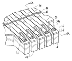
Referring to FIG. 6, a cover layer 40 of polyimide is formed over the conductor runs 26, over a region of the substrate that is to the rear, i.e. toward the support area 10, of the rectangular tip area 12 and a layer 44 of gold is deposited over the layer 40 by evaporation or sputtering. The layer 44 may be augmented by plating. The result of the fabrication steps described above is a multilayer structure that comprises the substrate 4, the gold film 14, the polyimide layer 16, the gold conductor runs 26, the polyimide layer 40, and the gold layer 44.
The tip area of the multilayer structure is then slit, whereby the tip area is divided into multiple separately flexible fingers 48 that project in cantilever fashion from the major portion of the structure. A given finger of the substrate may carry the distal end portion of a single conductor run, or it may carry the distal end portions of two adjacent conductor runs. The slitting of the tip area may be performed by ablation using a ultraviolet laser. The poor thermal conductivity of stainless steel is a favorable factor with regard to the laser ablation process. The width of the kerf that is removed is about 17 microns, so that the width of a finger is either about 108 microns or about 233 microns. The length of each finger is about 1 mm.
The structure shown in FIG. 6 may be used as a contact device for making electrical connection to contact pads of an electrical circuit device, such as an integrated circuit chip or a flat panel display device. The nickel bumps 34 serve as probe elements for contacting the connection pads of the circuit device. When the contact device is in use, each nickel bump contacts a single connection pad of the circuit device. A bump 34 a that is to contact a ground pad of the circuit device may be connected to the substrate by means of vias 46 formed in holes in the layer 16 before depositing the layer 20. Multiple vias 46 may be provided along the length of the conductor run 26 that ends at the bump 34 a in order to ensure that the contact bump 34 a is firmly grounded.
The configuration of the conductor runs and their spacing results in there being a stripline transmission line environment to the rear of the forward boundary of the layer 44, whereas there is a microstrip transmission line environment forward of the layer 44. Naturally, the slitting of the tip area results in degradation of the microstrip transmission line environment. In the case of the fingers being about 1 mm long, the microstrip transmission line environment extends to a point that is about 2 mm from the contact bumps. However the degradation is not so severe as to distort signals at frequencies below about 10 GHz to an unacceptable degree.
The structure shown in FIG. 6 may be used for probing a circuit device in a semiconductor tester, as will be described with reference to FIGS. 7-11.
Referring to FIG. 7, the tester comprises a prober 102 having a frame 102 a that serves as a mechanical ground. A device positioner 104 having a vacuum chuck 106 is mounted within or as part of the prober 102. The prober includes stepping motors (not shown) that act on the device positioner for translating the vacuum chuck relative to the frame 102 a in two perpendicular horizontal directions (X and Y) and vertically (Z), and for rotating the vacuum chuck about a vertical axis. The vacuum chuck holds a device under test, or DUT, 108. FIG. 7 illustrates the DUT 108 as a die that has previously been separated from other dice of the wafer in which it was fabricated, but it will be appreciated that, with appropriate modifications, the apparatus could be used for testing a semiconductor device at the wafer stage. As shown in FIG. 7, the DUT 108 has contact pads 112.
The tester also comprises a test head 116 that can be docked to the prober so that it is in a reliably reproducible position relative to the prober frame 102 a. The test head 116 includes an essentially rigid circuit board 122 (FIG. 8) that comprises an insulating substrate and conductor runs 126 exposed at the lower main face of the substrate. Vias (not shown) extend through the substrate and terminate at contact pads 128 that are exposed at the upper main face of the substrate. The circuit board 122 is removably held in the test head by screws that pass through holes 130 in the circuit board. When the test head 116 is docked in the prober 102 and the circuit board 122 is installed in the test head, the circuit board 122 is disposed horizontally and the contact pads 128 engage pogo pins 132, shown schematically in FIG. 7, by which the contact pads of the circuit board are connected to stimulus and response instruments (not shown), for purposes of conducting appropriate tests on the DUT.
A mounting plate 136 is secured to the circuit board 122. The mounting plate is positioned relative to the circuit board by guide pins 134 that project downward from the mounting plate and enter corresponding holes in the circuit board. The manner in which the mounting plate is attached to the circuit board will be described below.
The mounting plate has a generally cylindrical exterior surface of which the central axis 138 is considered to be the axis of the plate. The plate 136 is disposed with its axis 138 vertical and defines a cross-shaped through opening (FIG. 9) that is mirror image symmetrical about X-Z and Y-Z planes that intersect at the axis 138. At the outer end of each limb of the cross, the plate 136 is formed with a notch 140 that extends only part way through the plate and is bounded in the vertically downward direction by a horizontal surface 142.
A backup block 146 having the general shape, when viewed in plan, of a trapezoid seated on a rectangular base is positioned with its rectangular base in one of the notches 140. Similar backup blocks 148 are mounted in the other notches. The following description of the backup block 146 and associated components applies equally to the backup blocks 148.
The rectangular base of the backup block 146 has a planar mounting surface 150 (FIG. 7) that can be seated against the horizontal surface 142 at the bottom of the notch 140. For assembling the backup block 146 to the mounting plate 136, the backup block is formed with a hole 152 extruding through its rectangular base, and the mounting plate is formed with a blind hole 156 that is parallel to the axis of the mounting plate and enters the plate 136 at the horizontal surface 142. A guide pin 160 is inserted through the hole 152 in the backup block and into the blind hole 156 in the mounting plate, and in this manner the backup block is positioned with a moderate degree of precision relative to the mounting plate.
The backup block 146 is then attached to the mounting plate 136 by a vertical locking screw 164 (FIG. 8, FIG. 9A) that passes through a clearance hole 168 in the backup block 146 and enters a threaded bore 172 in the mounting plate 136 and a horizontal locking screw 176 (FIG. 7) that passes through a clearance hole 180 in the mounting plate and enters a threaded bore 184 in the backup block. The backup block 146 is thereby attached to the mounting plate, and the guide pin 160 is then removed. The clearance holes 168 and 180 allow a small degree of horizontal and vertical movement of the backup block relative to the mounting plate.
Two horizontal screws 186, which are horizontally spaced and disposed one on each side of the screw 176, are inserted through threaded holes in the peripheral wall of the plate 136 and enter blind clearance holes in the backup block. Similarly, two vertical screws 190, which are horizontally spaced and disposed one on each side of the screw 164, are inserted through threaded holes in the backup block 146 and engage the surface 142 of the mounting plate 136. The screws 176 and 186 can be used to adjust the horizontal position of the backup block relative to the mounting plate 136. By selectively turning the screws 176 and 186, the backup block can be advanced or retracted linearly and/or rotated about a vertical axis. In similar fashion, using screws 164 and 190, the backup block can be raised or lowered relative to the mounting plate and/or tilted about a horizontal axis. When the backup block is in the desired position and orientation, the locking screws are tightened.
The apparatus shown in FIGS. 7-10 also comprises a contact device 194 associated with the backup block 146. The contact device 194 is generally triangular and has two edges that converge from a support area toward a generally rectangular tip area. The tip area of the contact device is divided into multiple fingers that extend parallel to an axis of symmetry of the contact device. The contact device includes conductor runs that extend from the support area to the tip area, and one run extends along each finger in the tip area. At its support area, the conductor runs of the contact device are exposed on the underside of the contact device. The contact device may be fabricated by the method that is described above with reference to FIGS. 1-6.
Inboard of the rectangular base, the trapezoidal portion of the backup block 146 extends downward toward the central axis 138. The contact device 194 is disposed below the inclined lower surface of the backup block 146 and is positioned relative to the backup block by guide pins 202 (e.g., FIGS. 11A and 11B) that project from the backup block and pass through alignment holes 204 in the contact device. The manner in which the contact device is attached to the backup block will be described below.
The apparatus also comprises a flexible circuit 208 having an inner edge region 208A and an outer edge region 208B (e.g., FIG. 10). The flexible circuit comprises a substrate of polyimide or similar insulating material, a ground plane (not shown) on the lower side of the substrate, and multiple discrete conductor runs 210 on the upper side of the substrate. Over the inner edge region 208A, the spacing of the conductor runs 210 corresponds to the spacing of the conductor runs across the support area of the contact device 194, and over the outer edge region 208B, the spacing of the conductor runs 210 corresponds to the spacing of the conductor runs 126 along the inner edge of the printed circuit board 122.
The flexible circuit is formed with inner and outer pairs of alignment holes 214A and 214B. The inner pair of alignment holes 214A are threaded by the guide pins 202, whereby the inner edge region 208A is positioned relative to the contact device 194. Similarly, the outer pair of alignment holes 214B are threaded by the guide pins 134, whereby the outer edge region 208B of the flexible circuit is positioned relative to the printed circuit board. The flexible circuit is also formed with two sets of mounting holes 218A and 218B.
The support area of the contact device 194, the inner edge region 208A of the flexible circuit, and a first length 22A of Shinetsu strip are clamped between the backup block and a clamping plate 226A by means of screws 230A. The outer edge region 208B of the flexible circuit 208, the inner region of the printed circuit board 122, and a second length 222B of Shinetsu strip are clamped between the mounting plate 136 and a second clamping plate 226B by means of screws 230B. The positions of the alignment holes 214A and 214B relative to the conductor runs of the flexible circuit are such that the conductor runs 210 at the inner edge region 208A of the flexible circuit are in registration with the conductor runs 26 in the support area of the contact device, and the conductor runs 210 in the outer edge region 208B of the flexible circuit are in registration with the conductor runs 126 along the inner edge of the printed circuit board. The Shinetsu strip, the thickness of which is exaggerated in FIG. 7, is characterized by anisotropic electrical conductivity when compressed perpendicular to its length: its conductivity is very good in directions perpendicular to its own plate and is very bad in directions parallel to its own plane and to its length. Thus, the Shinetsu strip 222A connects the conductor runs 26 of the probe member 194 to respective conductor runs 210 of the flexible circuit 208, and the Shinetsu strip 222B connects the conductor runs 210 of the flexible circuit 208 to respective conductor runs 126 of the printed circuit board 122.
Tightening of the clamping screws compresses the Shinetsu strips, which then establish a good electrically conductive connection between the conductor runs of the contact device and the conductor runs 126 of the printed circuit board 122, through the Shinetsu strips and respective conductor runs of the flexible circuit 208.
As described with reference to FIGS. 1-6, the tip area of the contact device 194 is divided into fingers, each of which has a contact run that terminates in a contact bump. Since the tip area is spaced from the support area, at which the contact device is clamped to the backup block, the tip area can be deflected away from the plane of the underside of the backup block. Vertical adjustment screws 234 are fitted in respective threaded holes in the backup block 146. By appropriate adjustment of the screws 234, the contact device can be preloaded to a condition in which the contact device 194 is deflected downwards relative to the backup block 146, and by further adjustment of the screws 234 the tip area can be forced downward, or permitted to rise, or tilted about the axis 18. It is important to note that the “mechanical ground” therefore extends to a location of the contact device that is beyond the support area but does not extend as far as the lip area. As described more fully below, proper positioning of mechanical ground can enable stress sharing between the fingers of the contact device and the contact device substrate, thereby enabling the contact device to withstand the stresses that result from applying force sufficient to ensure reliable contact between the DUT and the contact device, given the irregularities that can be expected in actual devices/conditions.
When all four backup blocks are properly installed in the mounting plate 136, the tip portions of the four contact devices extend along four edges of a square and are positioned for making electrically conductive contact to the contact pads of the device under test. By observing the DUT through the opening defined between the inner ends of the four backup blocks, the DUT can be positioned for contacting the contact bumps when the DUT is raised by the positioning device.
When the DUT is raised relative to the test head, the contact pads of the DUT engage the contact bumps of the contact device. After initial contact has been established (first touchdown), the DUT is raised an initial 10-15 microns, which is sufficient to absorb any expected error in coplanarity of the contact bumps and contact pads and achieve last touchdown (each contact bump is in contact with its respective contact pad). The DUT is then raised by a further 75 microns. The spring rate of the fingers and the spring rate of the base region of the substrate, between the fingers and the support area, are such that the contact force exerted at each contact pad is at least 10 grams. The initial deflection of 10-15 microns is sufficient to provide a contact force of about 2 grams at a single finger, whereas the further deflection of 75 microns provides a contact force of N*10 grams, where N is the number of fingers, or 10 grams per finger. By sharing the deflection between the fingers and the base region of the substrate, a high degree of compliance may be achieved, allowing contact with all the contact bumps, without sacrificing the contact force that is needed to achieve a reliable electrical contact between the contact bumps and the fingers.
The elastic nature of the metal of the substrate ensures that when the DUT is brought into contact with the contact bumps, and is slightly over driven, deflection of the fingers provides a desirable scrubbing action and also supplies sufficient contact force for providing a reliable pressure contact between the contact bump and the connection pad of the DUT.
The film 14 of gold serves as the ground plane, and the substrate 4, although conductive, does not contribute to the electrical performance of the device.
It is should be particularly emphasized how the present invention achieves desirous stress load sharing between the fingers and the substrate. It has been determined that with available materials, to be of practical size and provide suitable compliance/deflection of the fingers (such as to accommodate deviations from coplanarity, etc.), stress loads induced in the fingers and the substrate should be balanced (i.e., maintained in an acceptable relative range, below the stress limit of the material). Proper positioning of a mechanical ground between the ends of the fingers and the back extremity of the support area can enable controlled balancing of the relative stress loads, while also ensuring an adequate deflection of the fingers to achieve adequate compliance. In preferred embodiments, the relative stress loads of the fingers and substrate are maintained/balanced in a ranges of about 0.7 to 1.3, 0.8 to 1.2 or 0.9 to 1.1. Other ranges may be utilized, provided that a desirable balance is maintained, while of meeting the conditions of adequate deflection/compliance in the fingers, while staying within the stress limits of the constant materials.
In combination with the stress load balancing, it also has been discovered that, with available materials, the length of the fingers, controlled by the length of the slit and overall physical geometry, etc., can be chosen to give the desired finger deflection/compliance, such as a desired deflection of greater than about 10 microns, 12, microns or 15 microns, in the case of, for example, 60-80 or 75 microns, etc., of overdrive, while maintaining stress balancing as described above, can produce a probe element that produces reliable connection with the DUT while surviving the resulting stress loads, etc.
The present invention may be desirably applied to the testing and manufacture of devices such as integrated circuits or displays (such as LCD panels). Initially, a manufacturing process for the DUT 108 is conducted, such as a planar-type integrated circuit manufacturing process. For display devices, an appropriate LCD or other manufacturing process is conducted. After such manufacturing, the DUT 108 on a positioning device, such as a vacuum chuck 106 of prober 102 (the DUT may be in wafer or die form, in the case of integrated circuits, etc.). The DUT 108 is aligned with contact device 194 to the extent required for proper placement. Thereafter, relative movement is effected of the DUT 108 with respect to the contact device 194 to establish initial contact therebetween (as determined electrically or by a known mechanical means). After initial contact, over-driving of the relative movement to a predetermined degree is conducted (such as described above) to establish reliable electrical connection, wherein stresses are desirably shared between the extended fingers of the contact device and the substrate of the contact device. Positioning of a mechanical ground as in the present invention is particularly desirous in this regards. Thereafter, test signals are applied to the DUT 108 and it is electrically determined whether the DUT is defective or otherwise within or outside acceptable specifications. The pass/fail condition of the DUT may be recorded (which may include mechanical notation, such as inking the DUT if defective, etc., or by data recording). Still thereafter, the DUT 108 may be removed from the positioning device. If the device is acceptable, known packaging and assembling of the DUT may be performed.
With the present invention, devices with connection points of fine pitch may be reliably tested and manufactured.
It will be appreciated that the invention is not restricted to the particular embodiment that has been described, and that variations may be made therein without departing from the scope of the invention as defined in the appended claims and equivalents thereof. For example, although the invention has been described with reference to the drawings in terms of strip line and microstrip transmission line environments, if the film 14 were omitted and every other conductor run 26 across the contact device were a ground conductor run, a combination of a microstrip and coplanar transmission line environment would be provided. If every other conductor run were not a ground run, a microstrip transmission line environment would be provided as far as the forward edge of the layer 44, and for some applications, it might be acceptable for the transmission line environment to terminate at this point, provided that it is quite close to the contact bumps. Application of the invention to a semiconductor tester has been described with reference to an implementation in which there is one contact bump on each finger of the contact device, and the use of individual fingers for each contact bump ensures maximum accommodation of non-coplanarity of the contact pads of the DUT. However, it might be advantageous to provide two contact bumps, each connected to its own conductor run, since torsion of the finger accommodates a difference in height of the respective contact pads, and the greater width of the finger provides substantially greater stiffness with respect to deflection. The invention is not limited to testing of devices prior to packaging and may he used for final testing of packaged devices, particularly a device that is packaged for surface mounting, since the terminals are then suitably positioned for engagement by the contact bumps. Further, numerical references, while giving unexpectedly desirable results in the preferred embodiments over prior art techniques, may be adjusted in other embodiments.

Claims (44)

What is claimed is:
1. A method comprising the steps of:
carrying out a device manufacturing process to produce an electronic device having electrically-responsive circuits;
positioning the electronic device on a positioning device;
effecting aligned relative movement of the device with respect to a contact device to establish initial contact therebetween, wherein the contact device includes contacts positioned on fingers having a length extending away from a support area on a substrate and a mechanical ground positioned between the fingers and the support area, wherein each of the fingers has one or two contacts formed thereon, wherein deflection resulting from contact between the contact device and the electronic device is shared between a portion of the substrate on which the fingers are formed and a portion of the substrate not including the fingers;
applying test signals to the electronic device and electrically determining whether the electronic device is defective;
recording whether the electronic device is defective;
removing the electronic device from the positioning device; and
packaging and assembling the electronic device if it is not defective.
2. The method of claim 1, wherein the electronic device comprises an integrated circuit.
3. The method of claim 2, wherein the test signals are applied when the integrated circuit are in wafer form.
4. The method of claim 1, wherein the fingers are about 125 μm in thickness.
5. The method of claim 1, wherein the connection points of the electronic devices are spaced to have a pitch of about 100 μm.
6. The method of claim 1, wherein the conductors are about 50 μm wide and the fingers are about 1 mm in length.
7. The method of claim 1, wherein the electronic device comprises an integrated circuit.
8. The method of claim, 1, wherein the fingers and the substrate each having a spring rate determined so that a predetermined minimum contact force is exerted on each of the connection points.
9. The method of claim 8, wherein the predetermined minimum contact force is about 10 grams.
10. The method of claim 1, wherein at least a portion of the conductors comprise striplines.
11. The method of claim 1, wherein one or more fingers having two contacts formed thereon undergo torsion to accommodate height differences between connection points of the electronic device.
12. A method comprising the steps of:
carrying out a device manufacturing process to produce an electronic device having electrically-responsive circuits;
positioning the electronic device on a positioning device;
effecting aligned relative movement of the device with respect to a contact device to establish initial contact therebetween, wherein the contact device includes contacts positioned on fingers having a length extending away from a support area on a substrate and a mechanical ground positioned between the fingers and the support area, wherein each of the fingers has one or two contacts formed thereon, wherein deflection resulting from contact between the contact device and the electronic device is shared between a portion of the substrate on which the fingers are formed and a portion of the substrate not including the fingers; and
applying test signals to the electronic device and electrically determining whether the electronic device is defective.
13. The method of claim 12, wherein the electronic device comprises an integrated circuit.
14. The method of claim 13, wherein the test signals are applied when the integrated circuit are in wafer form.
15. The method of claim 12, wherein the fingers are about 125 μm in thickness.
16. The method of claim 12, wherein the connection points of the electronic devices are spaced to have a pitch of about 100 μm.
17. The method of claim 12, wherein the conductors are about 50 μm wide and the fingers are about 1 mm in length.
18. The method of claim 12, wherein the electronic device comprises an integrated circuit.
19. The method of claim 12, wherein the fingers and the substrate each have a spring rate determined so that a predetermined minimum contact force is exerted on each of the connection points.
20. The method of claim 19, wherein the predetermined minimum contact force is about 10 grams.
21. The method of claim 12, wherein at least a portion of the conductors comprise striplines.
22. The method of claim 12, wherein one or more fingers having two contacts formed thereon undergo torsion to accommodate height differences between connection points of the electronic device.
23. A method comprising the steps of:
carrying out a device manufacturing process to produce an electronic device having electrically-responsive circuits;
positioning the electronic device on a positioning device;
effecting aligned relative movement of the device with respect to a contact device to establish initial contact therebetween, wherein the contact device includes contacts positioned on fingers having a length extending away from a support area on a substrate and including a contact portion that makes electrical contact with the electronic device, wherein a mechanical ground is positioned between the contact portion and the support area, wherein each of the fingers has one or two contacts formed thereon, wherein deflection resulting from contact between the contact device and the electronic device is shared between a portion of the substrate on which the fingers are formed and a portion of the substrate not including the fingers;
applying test signals to the electronic device and electrically determining whether the electronic device is defective;
recording whether the electronic device is defective;
removing the electronic device from the positioning device; and
packaging and assembling the electronic device if it is not defective.
24. The method of claim 23, wherein the electronic device comprises an integrated circuit.
25. The method of claim 24, wherein the test signals are applied when the integrated circuit are in wafer form.
26. The method of claim 23, wherein the fingers are about 125 μm in thickness.
27. The method of claim 23, wherein the connection points of the electronic devices are spaced to have a pitch of about 100 μm.
28. The method of claim 23, wherein the conductors are about 50 μm wide and the fingers are about 1 mm in length.
29. The method of claim 23, wherein the electronic device comprises an integrated circuit.
30. The method of claim 23, wherein the fingers and the substrate each have a spring rate determined so that a predetermined minimum contact force is exerted on each of the connection points.
31. The method of claim 30, wherein the predetermined minimum contact force is about 10 grams.
32. The method of claim 23, wherein at least a portion of the conductors comprise striplines.
33. The method of claim 23, wherein one or more fingers having two contacts formed thereon undergo torsion to accommodate height differences between connection points of the electronic device.
34. A method comprising the steps of:
carrying out a device manufacturing process to produce an electronic device having electrically-responsive circuits;
positioning the electronic device on a positioning device;
effecting aligned relative movement of the device with respect to a contact device to establish initial contact therebetween, wherein the contact device includes contacts positioned on fingers having a length extending away from a support area on a substrate and including a contact portion that makes electrical contact with the electronic device, wherein a mechanical ground is positioned between the contact portion and the support area, wherein each of the fingers has one or two contacts formed thereon, wherein deflection resulting from contact between the contact device and the electronic device is shared between a portion of the substrate on which the fingers are formed and a portion of the substrate not including the fingers;
applying test signals to the electronic device and electrically determining whether the electronic device is defective.
35. The method of claim 34, wherein the electronic device comprises an integrated circuit.
36. The method of claim 35, wherein the test signals are applied when the integrated circuit are in wafer form.
37. The method of claim 34, wherein the fingers are about 125 μm in thickness.
38. The method of claim 34, wherein the connection points of the electronic devices are spaced to have a pitch of about 100 μm.
39. The method of claim 34, wherein the conductors are about 50 μm wide and the fingers are about 1 mm in length.
40. The method of claim 34, wherein the electronic device comprises an integrated circuit.
41. The method of claim 34, wherein the fingers and the substrate each have a spring rate determined so that a predetermined minimum contact force is exerted on each of the connection points.
42. The method of claim 41, wherein the predetermined minimum contact force is about 10 grams.
43. The method of claim 34, wherein at least a portion of the conductors comprise striplines.
44. The method of claim 34, wherein one or more fingers having two contacts formed thereon undergo torsion to accommodate height differences between connection points of the electronic device.
US09/512,784 2000-02-25 2000-02-25 Method of manufacturing and testing an electronic device using a contact device having fingers and a mechanical ground Expired - Fee Related US6496026B1 (en)

Priority Applications (1)

Application Number Priority Date Filing Date Title
US09/512,784 US6496026B1 (en) 2000-02-25 2000-02-25 Method of manufacturing and testing an electronic device using a contact device having fingers and a mechanical ground

Applications Claiming Priority (1)

Application Number Priority Date Filing Date Title
US09/512,784 US6496026B1 (en) 2000-02-25 2000-02-25 Method of manufacturing and testing an electronic device using a contact device having fingers and a mechanical ground

Related Parent Applications (2)

Application Number Title Priority Date Filing Date
US08/765,661 Division US6046599A (en) 1996-05-20 1996-05-20 Method and device for making connection
PCT/US1996/007359 Division WO1996036884A1 (en) 1995-05-19 1996-05-20 Method and device for making connection

Publications (1)

Publication Number Publication Date
US6496026B1 true US6496026B1 (en) 2002-12-17

Family

ID=24040545

Family Applications (1)

Application Number Title Priority Date Filing Date
US09/512,784 Expired - Fee Related US6496026B1 (en) 2000-02-25 2000-02-25 Method of manufacturing and testing an electronic device using a contact device having fingers and a mechanical ground

Country Status (1)

Country Link
US (1) US6496026B1 (en)

Cited By (25)

* Cited by examiner, † Cited by third party
Publication number Priority date Publication date Assignee Title
US20030048624A1 (en) * 2001-08-22 2003-03-13 Tessera, Inc. Low-height multi-component assemblies
WO2003032370A2 (en) * 2001-10-09 2003-04-17 Tessera, Inc. Stacked packages
US6622289B2 (en) * 1998-09-15 2003-09-16 Microconnect, Llc Methods for making contact device for making connection to an electronic circuit device and methods of using the same
US20040056674A1 (en) * 1998-07-08 2004-03-25 Capres Aps Multi-point probe
US20040104470A1 (en) * 2002-08-16 2004-06-03 Tessera, Inc. Microelectronic packages with self-aligning features
US20040262777A1 (en) * 2002-10-11 2004-12-30 Tessera, Inc. Components, methods and assemblies for multi-chip packages
US20060103369A1 (en) * 2004-11-04 2006-05-18 Josef Gluch Apparatus and method for making ground connection
US20060214282A1 (en) * 2005-03-22 2006-09-28 Mitsui Mining & Smelting Co., Ltd. Flexible printed wiring board, method for fabricating flexible printed wiring board, and semiconductor device
US20060290367A1 (en) * 2005-06-24 2006-12-28 Formfactor, Inc. Method and apparatus for adjusting a multi-substrate probe structure
WO2007089543A2 (en) * 2006-01-27 2007-08-09 Xandex, Inc. Active probe contact array management
US20090033348A1 (en) * 2007-08-01 2009-02-05 Gunsei Kimoto Electrical signal connector
US20100182031A1 (en) * 2004-05-21 2010-07-22 Microprobe, Inc. Layered Probes With Core
US7935569B2 (en) 2002-09-06 2011-05-03 Tessera, Inc. Components, methods and assemblies for stacked packages
US8230593B2 (en) 2008-05-29 2012-07-31 Microprobe, Inc. Probe bonding method having improved control of bonding material
US8324923B2 (en) 2007-04-10 2012-12-04 Microprobe, Inc. Vertical probe array arranged to provide space transformation
US8415963B2 (en) 2005-12-07 2013-04-09 Microprobe, Inc. Low profile probe having improved mechanical scrub and reduced contact inductance
USRE44407E1 (en) 2006-03-20 2013-08-06 Formfactor, Inc. Space transformers employing wire bonds for interconnections with fine pitch contacts
US8723546B2 (en) 2007-10-19 2014-05-13 Microprobe, Inc. Vertical guided layered probe
US8907689B2 (en) 2006-10-11 2014-12-09 Microprobe, Inc. Probe retention arrangement
US8988091B2 (en) 2004-05-21 2015-03-24 Microprobe, Inc. Multiple contact probes
USRE45463E1 (en) 2003-11-12 2015-04-14 Tessera, Inc. Stacked microelectronic assemblies with central contacts
CN104733355A (en) * 2013-12-23 2015-06-24 朗姆研究公司 Robot with integrated aligner
US9121868B2 (en) 2004-07-09 2015-09-01 Formfactor, Inc. Probes with offset arm and suspension structure
US9476911B2 (en) 2004-05-21 2016-10-25 Microprobe, Inc. Probes with high current carrying capability and laser machining methods
USRE46221E1 (en) 2004-05-21 2016-11-29 Microprobe, Inc. Probe skates for electrical testing of convex pad topologies

Citations (47)

* Cited by examiner, † Cited by third party
Publication number Priority date Publication date Assignee Title
US3405361A (en) 1964-01-08 1968-10-08 Signetics Corp Fluid actuable multi-point microprobe for semiconductors
US3810016A (en) 1971-12-17 1974-05-07 Western Electric Co Test probe for semiconductor devices
US3832632A (en) 1971-11-22 1974-08-27 F Ardezzone Multi-point probe head assembly
US3851249A (en) 1973-06-04 1974-11-26 Electroglass Inc Microcircuit test device with multi-axes probe control and probe stop means
US3866119A (en) 1973-09-10 1975-02-11 Probe Rite Inc Probe head-probing machine coupling adaptor
US4035723A (en) 1975-10-16 1977-07-12 Xynetics, Inc. Probe arm
US4161692A (en) 1977-07-18 1979-07-17 Cerprobe Corporation Probe device for integrated circuit wafers
US4574235A (en) 1981-06-05 1986-03-04 Micro Component Technology, Inc. Transmission line connector and contact set assembly for test site
US4585727A (en) 1984-07-27 1986-04-29 Probe-Tronics, Inc. Fixed point method and apparatus for probing semiconductor devices
US4588241A (en) 1983-09-23 1986-05-13 Probe-Rite, Inc. Surface mating coaxial connector
US4636722A (en) 1984-05-21 1987-01-13 Probe-Rite, Inc. High density probe-head with isolated and shielded transmission lines
EP0220830A2 (en) 1985-09-26 1987-05-06 Tektronix, Inc. Wafer probe head, and method of assembling a wafer probe head
US4673839A (en) 1986-09-08 1987-06-16 Tektronix, Inc. Piezoelectric pressure sensing apparatus for integrated circuit testing stations
EP0230348A2 (en) 1986-01-07 1987-07-29 Hewlett-Packard Company Test probe
US4697143A (en) 1984-04-30 1987-09-29 Cascade Microtech, Inc. Wafer probe
US4749942A (en) 1985-09-26 1988-06-07 Tektronix, Inc. Wafer probe head
US4751457A (en) 1986-09-08 1988-06-14 Tektronix, Inc. Integrated circuit probe parallelism establishing method and apparatus
US4758785A (en) 1986-09-03 1988-07-19 Tektronix, Inc. Pressure control apparatus for use in an integrated circuit testing station
EP0276900A2 (en) 1987-01-30 1988-08-03 Hewlett-Packard Company Apparatus and method for aligning two surfaces
US4764723A (en) 1986-11-10 1988-08-16 Cascade Microtech, Inc. Wafer probe
EP0283219A2 (en) 1987-03-11 1988-09-21 Hewlett-Packard Company Apparatus for automatically scrubbing a surface
US4829233A (en) 1987-03-09 1989-05-09 United Kingdom Atomic Energy Authority Microwave probe
US4829242A (en) 1987-12-07 1989-05-09 Microelectronics And Computer Technology Corporation Multigigahertz probe
EP0331282A1 (en) 1988-03-01 1989-09-06 Hewlett-Packard Company Membrane-based IC test probe with precisely positioned contacts
US4891585A (en) 1986-09-05 1990-01-02 Tektronix, Inc. Multiple lead probe for integrated circuits in wafer form
US4894612A (en) 1987-08-13 1990-01-16 Hypres, Incorporated Soft probe for providing high speed on-wafer connections to a circuit
US4899099A (en) 1988-05-19 1990-02-06 Augat Inc. Flex dot wafer probe
US4904933A (en) 1986-09-08 1990-02-27 Tektronix, Inc. Integrated circuit probe station
US4906920A (en) 1988-10-11 1990-03-06 Hewlett-Packard Company Self-leveling membrane probe
US4912399A (en) 1987-06-09 1990-03-27 Tektronix, Inc. Multiple lead probe for integrated circuits in wafer form
EP0360396A2 (en) 1988-09-23 1990-03-28 Hewlett-Packard Company Force delivery system for improved precision membrane probe
EP0361779A1 (en) 1988-09-26 1990-04-04 Hewlett-Packard Company Micro-strip architecture for membrane test probe
US4918383A (en) 1987-01-20 1990-04-17 Huff Richard E Membrane probe with automatic contact scrub action
US4943768A (en) 1986-12-12 1990-07-24 Mitsubishi Denki Kabushiki Kaisha Testing device for electrical circuit boards
US4975638A (en) 1989-12-18 1990-12-04 Wentworth Laboratories Test probe assembly for testing integrated circuit devices
JPH03165033A (en) 1989-11-24 1991-07-17 Seiko Epson Corp Apparatus for lifting substrate from super pure water and drying substrate
US5061894A (en) 1988-10-25 1991-10-29 Tokyo Electron Limited Probe device
US5191708A (en) 1990-06-20 1993-03-09 Hitachi, Ltd. Manufacturing method of a probe head for semiconductor LSI inspection apparatus
US5221895A (en) 1991-12-23 1993-06-22 Tektronix, Inc. Probe with microstrip transmission lines
US5355080A (en) 1989-08-07 1994-10-11 Giga Probe, Inc. Multi-point probe assembly for testing electronic device
US5414371A (en) 1993-03-25 1995-05-09 Probes Associates, Inc. Semiconductor device test probe ring apparatus and method of manufacture
US5416429A (en) 1994-05-23 1995-05-16 Wentworth Laboratories, Inc. Probe assembly for testing integrated circuits
US5479110A (en) * 1994-01-13 1995-12-26 Advanpro Corporation Printed flexible circuit terminations and method of manufacture
US5489855A (en) 1990-08-22 1996-02-06 Poisel; C. Edward Apparatus and process providing controlled probing
US5528159A (en) 1993-06-14 1996-06-18 International Business Machine Corp. Method and apparatus for testing integrated circuit chips
US5565788A (en) * 1994-07-20 1996-10-15 Cascade Microtech, Inc. Coaxial wafer probe with tip shielding
US5621333A (en) * 1995-05-19 1997-04-15 Microconnect, Inc. Contact device for making connection to an electronic circuit device

Patent Citations (49)

* Cited by examiner, † Cited by third party
Publication number Priority date Publication date Assignee Title
US3405361A (en) 1964-01-08 1968-10-08 Signetics Corp Fluid actuable multi-point microprobe for semiconductors
US3832632A (en) 1971-11-22 1974-08-27 F Ardezzone Multi-point probe head assembly
US3810016A (en) 1971-12-17 1974-05-07 Western Electric Co Test probe for semiconductor devices
US3851249A (en) 1973-06-04 1974-11-26 Electroglass Inc Microcircuit test device with multi-axes probe control and probe stop means
US3866119A (en) 1973-09-10 1975-02-11 Probe Rite Inc Probe head-probing machine coupling adaptor
US4035723A (en) 1975-10-16 1977-07-12 Xynetics, Inc. Probe arm
US4161692A (en) 1977-07-18 1979-07-17 Cerprobe Corporation Probe device for integrated circuit wafers
US4574235A (en) 1981-06-05 1986-03-04 Micro Component Technology, Inc. Transmission line connector and contact set assembly for test site
US4588241A (en) 1983-09-23 1986-05-13 Probe-Rite, Inc. Surface mating coaxial connector
US4697143A (en) 1984-04-30 1987-09-29 Cascade Microtech, Inc. Wafer probe
US4636722A (en) 1984-05-21 1987-01-13 Probe-Rite, Inc. High density probe-head with isolated and shielded transmission lines
US4585727A (en) 1984-07-27 1986-04-29 Probe-Tronics, Inc. Fixed point method and apparatus for probing semiconductor devices
EP0220830A2 (en) 1985-09-26 1987-05-06 Tektronix, Inc. Wafer probe head, and method of assembling a wafer probe head
US4749942A (en) 1985-09-26 1988-06-07 Tektronix, Inc. Wafer probe head
EP0230348A2 (en) 1986-01-07 1987-07-29 Hewlett-Packard Company Test probe
US4758785A (en) 1986-09-03 1988-07-19 Tektronix, Inc. Pressure control apparatus for use in an integrated circuit testing station
US4891585A (en) 1986-09-05 1990-01-02 Tektronix, Inc. Multiple lead probe for integrated circuits in wafer form
US4673839A (en) 1986-09-08 1987-06-16 Tektronix, Inc. Piezoelectric pressure sensing apparatus for integrated circuit testing stations
US4751457A (en) 1986-09-08 1988-06-14 Tektronix, Inc. Integrated circuit probe parallelism establishing method and apparatus
US4904933A (en) 1986-09-08 1990-02-27 Tektronix, Inc. Integrated circuit probe station
US4764723A (en) 1986-11-10 1988-08-16 Cascade Microtech, Inc. Wafer probe
US4943768A (en) 1986-12-12 1990-07-24 Mitsubishi Denki Kabushiki Kaisha Testing device for electrical circuit boards
US4918383A (en) 1987-01-20 1990-04-17 Huff Richard E Membrane probe with automatic contact scrub action
EP0276900A2 (en) 1987-01-30 1988-08-03 Hewlett-Packard Company Apparatus and method for aligning two surfaces
US4829233A (en) 1987-03-09 1989-05-09 United Kingdom Atomic Energy Authority Microwave probe
EP0283219A2 (en) 1987-03-11 1988-09-21 Hewlett-Packard Company Apparatus for automatically scrubbing a surface
EP0369554A2 (en) 1987-03-11 1990-05-23 Hewlett-Packard Company Apparatus for automatically scrubbing a surface
US4912399A (en) 1987-06-09 1990-03-27 Tektronix, Inc. Multiple lead probe for integrated circuits in wafer form
US4894612A (en) 1987-08-13 1990-01-16 Hypres, Incorporated Soft probe for providing high speed on-wafer connections to a circuit
US4829242A (en) 1987-12-07 1989-05-09 Microelectronics And Computer Technology Corporation Multigigahertz probe
EP0331282A1 (en) 1988-03-01 1989-09-06 Hewlett-Packard Company Membrane-based IC test probe with precisely positioned contacts
US4980637A (en) 1988-03-01 1990-12-25 Hewlett-Packard Company Force delivery system for improved precision membrane probe
US4899099A (en) 1988-05-19 1990-02-06 Augat Inc. Flex dot wafer probe
EP0360396A2 (en) 1988-09-23 1990-03-28 Hewlett-Packard Company Force delivery system for improved precision membrane probe
EP0361779A1 (en) 1988-09-26 1990-04-04 Hewlett-Packard Company Micro-strip architecture for membrane test probe
US4906920A (en) 1988-10-11 1990-03-06 Hewlett-Packard Company Self-leveling membrane probe
US5061894A (en) 1988-10-25 1991-10-29 Tokyo Electron Limited Probe device
US5355080A (en) 1989-08-07 1994-10-11 Giga Probe, Inc. Multi-point probe assembly for testing electronic device
JPH03165033A (en) 1989-11-24 1991-07-17 Seiko Epson Corp Apparatus for lifting substrate from super pure water and drying substrate
US4975638A (en) 1989-12-18 1990-12-04 Wentworth Laboratories Test probe assembly for testing integrated circuit devices
US5191708A (en) 1990-06-20 1993-03-09 Hitachi, Ltd. Manufacturing method of a probe head for semiconductor LSI inspection apparatus
US5489855A (en) 1990-08-22 1996-02-06 Poisel; C. Edward Apparatus and process providing controlled probing
US5221895A (en) 1991-12-23 1993-06-22 Tektronix, Inc. Probe with microstrip transmission lines
US5414371A (en) 1993-03-25 1995-05-09 Probes Associates, Inc. Semiconductor device test probe ring apparatus and method of manufacture
US5528159A (en) 1993-06-14 1996-06-18 International Business Machine Corp. Method and apparatus for testing integrated circuit chips
US5479110A (en) * 1994-01-13 1995-12-26 Advanpro Corporation Printed flexible circuit terminations and method of manufacture
US5416429A (en) 1994-05-23 1995-05-16 Wentworth Laboratories, Inc. Probe assembly for testing integrated circuits
US5565788A (en) * 1994-07-20 1996-10-15 Cascade Microtech, Inc. Coaxial wafer probe with tip shielding
US5621333A (en) * 1995-05-19 1997-04-15 Microconnect, Inc. Contact device for making connection to an electronic circuit device

Cited By (50)

* Cited by examiner, † Cited by third party
Publication number Priority date Publication date Assignee Title
US20040056674A1 (en) * 1998-07-08 2004-03-25 Capres Aps Multi-point probe
US7323890B2 (en) * 1998-07-08 2008-01-29 Capres Aps Multi-point probe
US6957405B2 (en) * 1998-09-15 2005-10-18 Microconnect Llc Methods for manufacturing an electronic device having an electronically determined physical test member
US6622289B2 (en) * 1998-09-15 2003-09-16 Microconnect, Llc Methods for making contact device for making connection to an electronic circuit device and methods of using the same
US20040034839A1 (en) * 1998-09-15 2004-02-19 Saunders J. Lynn Methods for making contact device for making connection to an electronic circuit device and methods of using the same
US20030048624A1 (en) * 2001-08-22 2003-03-13 Tessera, Inc. Low-height multi-component assemblies
WO2003032370A2 (en) * 2001-10-09 2003-04-17 Tessera, Inc. Stacked packages
WO2003032370A3 (en) * 2001-10-09 2003-11-06 Tessera Inc Stacked packages
US20040203190A1 (en) * 2001-10-09 2004-10-14 Tessera, Inc. Stacked packages
US6913949B2 (en) 2001-10-09 2005-07-05 Tessera, Inc. Stacked packages
US7053485B2 (en) 2002-08-16 2006-05-30 Tessera, Inc. Microelectronic packages with self-aligning features
US20040104470A1 (en) * 2002-08-16 2004-06-03 Tessera, Inc. Microelectronic packages with self-aligning features
US7935569B2 (en) 2002-09-06 2011-05-03 Tessera, Inc. Components, methods and assemblies for stacked packages
US20070166876A1 (en) * 2002-10-11 2007-07-19 Tessera, Inc. Components, methods and assemblies for multi-chip packages
US7061122B2 (en) 2002-10-11 2006-06-13 Tessera, Inc. Components, methods and assemblies for multi-chip packages
US20040262777A1 (en) * 2002-10-11 2004-12-30 Tessera, Inc. Components, methods and assemblies for multi-chip packages
USRE45463E1 (en) 2003-11-12 2015-04-14 Tessera, Inc. Stacked microelectronic assemblies with central contacts
US8988091B2 (en) 2004-05-21 2015-03-24 Microprobe, Inc. Multiple contact probes
US9097740B2 (en) * 2004-05-21 2015-08-04 Formfactor, Inc. Layered probes with core
USRE46221E1 (en) 2004-05-21 2016-11-29 Microprobe, Inc. Probe skates for electrical testing of convex pad topologies
US9316670B2 (en) 2004-05-21 2016-04-19 Formfactor, Inc. Multiple contact probes
US9476911B2 (en) 2004-05-21 2016-10-25 Microprobe, Inc. Probes with high current carrying capability and laser machining methods
US20100182031A1 (en) * 2004-05-21 2010-07-22 Microprobe, Inc. Layered Probes With Core
US9121868B2 (en) 2004-07-09 2015-09-01 Formfactor, Inc. Probes with offset arm and suspension structure
US20060103369A1 (en) * 2004-11-04 2006-05-18 Josef Gluch Apparatus and method for making ground connection
US7161365B2 (en) 2004-11-04 2007-01-09 Infineon Technologies Ag Apparatus and method for making ground connection
US20060214282A1 (en) * 2005-03-22 2006-09-28 Mitsui Mining & Smelting Co., Ltd. Flexible printed wiring board, method for fabricating flexible printed wiring board, and semiconductor device
US20060290367A1 (en) * 2005-06-24 2006-12-28 Formfactor, Inc. Method and apparatus for adjusting a multi-substrate probe structure
US7845072B2 (en) * 2005-06-24 2010-12-07 Formfactor, Inc. Method and apparatus for adjusting a multi-substrate probe structure
US20090158586A1 (en) * 2005-06-24 2009-06-25 Formfactor, Inc. Method and apparatus for adjusting a multi-substrate probe structure
US7471094B2 (en) 2005-06-24 2008-12-30 Formfactor, Inc. Method and apparatus for adjusting a multi-substrate probe structure
WO2007002249A3 (en) * 2005-06-24 2007-11-22 Formfactor Inc Method and apparatus for adjusting a multi-substrate probe structure
US8415963B2 (en) 2005-12-07 2013-04-09 Microprobe, Inc. Low profile probe having improved mechanical scrub and reduced contact inductance
WO2007089543A2 (en) * 2006-01-27 2007-08-09 Xandex, Inc. Active probe contact array management
WO2007089543A3 (en) * 2006-01-27 2008-04-10 Xandex Inc Active probe contact array management
USRE44407E1 (en) 2006-03-20 2013-08-06 Formfactor, Inc. Space transformers employing wire bonds for interconnections with fine pitch contacts
US9310428B2 (en) 2006-10-11 2016-04-12 Formfactor, Inc. Probe retention arrangement
US8907689B2 (en) 2006-10-11 2014-12-09 Microprobe, Inc. Probe retention arrangement
US9274143B2 (en) 2007-04-10 2016-03-01 Formfactor, Inc. Vertical probe array arranged to provide space transformation
US8324923B2 (en) 2007-04-10 2012-12-04 Microprobe, Inc. Vertical probe array arranged to provide space transformation
CN101359000B (en) * 2007-08-01 2012-07-04 木本军生 Electrical signal connector
US7622937B2 (en) * 2007-08-01 2009-11-24 Gunsei Kimoto Electrical signal connector
US20090033348A1 (en) * 2007-08-01 2009-02-05 Gunsei Kimoto Electrical signal connector
US8723546B2 (en) 2007-10-19 2014-05-13 Microprobe, Inc. Vertical guided layered probe
US8230593B2 (en) 2008-05-29 2012-07-31 Microprobe, Inc. Probe bonding method having improved control of bonding material
US20150179488A1 (en) * 2013-12-23 2015-06-25 Lam Research Corporation Robot with integrated aligner
CN104733355A (en) * 2013-12-23 2015-06-24 朗姆研究公司 Robot with integrated aligner
US9299598B2 (en) * 2013-12-23 2016-03-29 Lam Research Corp. Robot with integrated aligner
CN104733355B (en) * 2013-12-23 2019-07-05 朗姆研究公司 Robot with integrated aligner
KR20210049072A (en) * 2013-12-23 2021-05-04 램 리써치 코포레이션 Robot with integrated aligner

Similar Documents

Publication Publication Date Title
US6046599A (en) Method and device for making connection
EP0781419B1 (en) Method and device for making connection
US6496026B1 (en) Method of manufacturing and testing an electronic device using a contact device having fingers and a mechanical ground
US5828226A (en) Probe card assembly for high density integrated circuits
US6343369B1 (en) Methods for making contact device for making connection to an electronic circuit device and methods of using the same
US6359456B1 (en) Probe card and test system for semiconductor wafers
US6798224B1 (en) Method for testing semiconductor wafers
US7517707B2 (en) Manufacturing method of semiconductor integrated circuit device and probe card
US5221895A (en) Probe with microstrip transmission lines
US20080029763A1 (en) Transmission Circuit, Connecting Sheet, Probe Sheet, Probe Card, Semiconductor Inspection System and Method of Manufacturing Semiconductor Device
JPH0517705B2 (en)
US7217139B2 (en) Interconnect assembly for a probe card
US7382143B2 (en) Wafer probe interconnect system
EP0304868A2 (en) Multiple lead probe for integrated circuits in wafer form
US20150362551A1 (en) Methods for Making Contact Device for Making Connection to an Electronic Circuit Device and Methods of Using the Same
KR100266389B1 (en) Contact carriers(tiles) for populating larger substrates with spring contacts
JPH04294559A (en) Probe card
JP3446636B2 (en) Contact probe and probe device
JPH10339740A (en) Probe device

Legal Events

Date Code Title Description
FPAY Fee payment

Year of fee payment: 4

AS Assignment

Owner name: MICROCONNECT LLC, CALIFORNIA

Free format text: ASSIGNMENT OF ASSIGNORS INTEREST;ASSIGNOR:MICROCONNECT, INC.;REEL/FRAME:020261/0936

Effective date: 20040527

Owner name: MICROCONNECT LLC, CALIFORNIA

Free format text: ASSIGNMENT OF ASSIGNORS INTEREST;ASSIGNOR:MICROCONNECT, INC.;REEL/FRAME:020243/0964

Effective date: 20040527

FPAY Fee payment

Year of fee payment: 8

REMI Maintenance fee reminder mailed
LAPS Lapse for failure to pay maintenance fees
STCH Information on status: patent discontinuation

Free format text: PATENT EXPIRED DUE TO NONPAYMENT OF MAINTENANCE FEES UNDER 37 CFR 1.362

FP Lapsed due to failure to pay maintenance fee

Effective date: 20141217